Abstract
The high efficiency and low cost of production of perovskite solar cells (PSCs) based on organic-inorganic halides have attracted the attention of researchers. However, due to the intricacy in the synthesis of Spiro-OMeTAD and the high cost of gold (Au) utilized as the back contact (BC), have affected its viability for commercialization. In this present study, a simulation was performed with and without HTM utilizing different metal contacts (Ag, Cr, Cu, Au, Ni and Pt). SCAPS-1D, a software program in one dimension, was used to conduct the simulation. A systematic analysis was done to determine how the metal back contact's work functions affected the PSC both with and without HTM. The outcomes demonstrate that the PSCs' photovoltaic performance is significantly influenced by the metal contact's work function (WF). The best metal contact for HTM and HTM-free devices was Pt, with a metal work function of 5.65 eV. The initial power conversion efficiencies (PCEs) for the two configurations were 26.229% for HTM-free and 25.608% for HTM-based device. A number of parameters, including absorber thickness, interface defect density, and electron transport material (ETM) thickness, were varied to obtain optimal values of 0.8 μm for both HTM and HTM-free PSCs, 1005 cm−2 for both HTM and HTM-free PSCs, and 0.01 μm for both HTM and HTM-free PSCs. These values were then used to simulate the final HTM and HTM-free devices with a PCE of 27.423%, current density (Jsc) of 27.546 mA/cm2, open circuit voltage (Voc) of 1.239 V, and fill factor (FF) of 80.347% for HTM-free whereas PCE of 26.767% with Jsc of 27.545 mA/cm2, Voc of 1.250 V, and FF of 77.733% for HTM based. These outcomes reflect outstanding enhancement of ∼1.05 and ∼1.07 times in PCE and Jsc over unoptimized cells with and without HTM.
Keywords: Perovskite solar cells, Defect density, HTM, Metal contact, SCAPS-1D
1. Introduction
At present, the demand of energy is satisfied by 80% of fossil fuel. However, it causes a serious depletion in crude reserves along with undesirable environmental effects as such prompted significant interest for alternative energy sources [[1], [2], [3], [4]].
Perovskite Solar Cells as an alternative energy source can mitigate the problem connected to the energy crisis and global environment due to their unique properties that have attracted attention of researchers, among which include; high coefficient of absorption, outstanding career mobility, high diffusion length of electrons and holes, good career lifetime, low excitation binding energy, and large value of dielectric constant [[5], [6], [7]]. Since after its invention by Kojima et al. [8], a lot of investments in research have been done leading to a present certified record PCE exceeding 25% [5,9]. Despite all the achievements attained, there are still some factors that have rendered it incapacitated for commercial viability.
Studying the impact of the operating mechanism of a perovskite solar cell is essential to achieving the best performance possible. But there is still a lot of information about the interface band offset and the metal's WF in perovskite solar cells that needs to be re-examined. In typical PSCs, a metal electrode is anticipated to have three main characteristics: (i) it shouldn't create a Schottky junction; (ii) it should have good conductivity; and (iii) it shouldn't react with the contact materials. Although Au (5.10 eV) is typically used as the back contact in PSC devices, other metals such as Ag (4.26 eV), C (5.00 eV), Cu (4.53 eV), W (4.32 eV), Al (4.28 eV), Ni (5.04 eV), Mo (4.36 eV), Ni (5.04 eV), and Pt (5.65 eV) have also been used and produced varied performance results [7,[10], [11], [12], [13], [14], [15], [16], [17]]. The standard Au metal contact requires a high-technology manufacture and development procedure (like a high-vacuum evaporation technique), and Au reacts with iodine-containing perovskite compounds to generate (AuI2)− and AuI3, which cause the gold electrode to degrade more quickly. Additionally, when perovskites, such as MAPbI3, are decomposed by UV radiation, a quick reaction occurs with gold to form MA2Au2I6, a phase with tetragonal symmetry that can infiltrate through HTM and contribute to the deterioration of the devices [18,19]. Most experimental researches done in PSCs are carried out without proper simulation to ascertain the optimized layers' properties before lab-scale development which can result to inferior device performance. Simulation and optimization are required to create a PSCs that is both highly efficient and ecologically friendly. Simulation is an essential tool for gaining a thorough understanding of the physical workings of solar cell devices, assessing the validity of given physical explanations, and determining the impact of physical modifications on performance. It can minimize not only the risk, time and money but also analyzes the attribute and role of layers to optimize the solar cell to best performance. Under optimized conditions, better metric parameters (Jsc, Voc, FF and PCE) can be realized.
In this present paper, the effect of different metal contact with different work function was examined systematically through device simulation with Ni, Cu, Cr, Ag and Pt as metal electrodes. The PSCs under study were simulated with and without the HTM layer to see how metal's WF affects recombination at the interfaces of perovskite and BC or at the interface of the HTM layer with BC. We studied how these interfacial events affect the cells' Jsc, Voc, FF, and PCE.
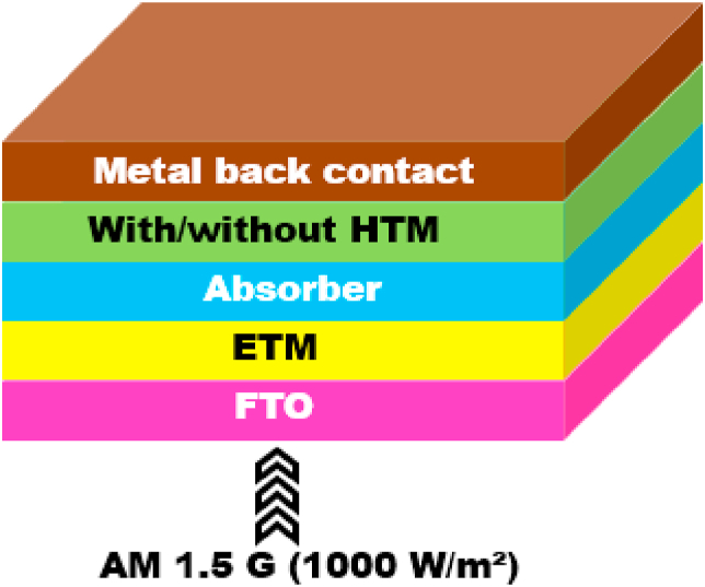
Specifically, the experimental work demonstrated by Behrouznejad et al. [7] was considered for calibration in this work, where we used TiO2 nanoparticles to aid the electron extraction, the perovskite nanocrystals (CH3NH3PbI3) to produce e-h pairs when energetic photons are absorbed, and spiro-OMeTAD to extract holes. The device structure used in the simulation is as shown in Fig. 1. The WF of the back contact is studied to determine their influence on the device performance. After assessing the most efficient device with its work function, the influence of absorber thickness, interface defect density and ETM thickness is explored in order to get an optimized value for the PCE. Based on the results presented we provided some useful guidance and recommendations in the design of lead-based PSCs, either with or without hole transport material.
Fig. 1.
The simulated device structure of the perovskite solar cell.
2. Device simulation
In this article, solar cell capacitance simulator (SCAPS-1D) software was deployed as the tool to simulate the proposed device. Some simulation softwares for computational study apart from SCAPS-1D include; SILVACO ATLAS, COMSOL, AMPS-1D, SETFOS [13,[20], [21], [22]]. Amongst the listed, SCAPS-1D has some advantages that made it subject of choice over others which include; user friendliness, simulation under the dark and under illumination conditions, and the fact that up to seven layer's heterojunction can be designed and simulated without routine measurements (C–V, C-f) [5]. The performance metrics of a solar cell such as PCE, FF, Jsc, and Voc as well as the incident to photon conversion efficiency (IPCE), energy band gap can be predicted simply by solving the three basic equations of semiconductor (equations (1), (2), (3))) [5,23];
| (1) |
| (2) |
| (3) |
where and denote the ionized donor doping concentration and the ionized acceptor doping concentration, respectively. Trapped holes are , while the free electrons are , and finally the free holes are . The electron charge is q, permittivity is , the electron diffusion coefficient is D, the rate of generation is G, the electric force field is E, the electron charge is q, and the electrostatic potential is . Fig. 1 depicts the structure of the device, which consists of Ag, Cr, Cu, Au, Ni, and Pt as back contacts; spiro-OMeTAD as HTL; FTO as left contact; TiO2 as ETL; and CH3NH3PbI3 as a light-absorbing material.
This structure of PSC was used to study the effect of metal back contact in HTM based PSC with the purpose of obtaining the optimum metal contact for further optimization of layer's parameters. Same was done in the device without HTM. Ag = 4.47, Cr = 4.50, Cu = 4.65, Au = 5.10, Ni = 5.15, and Pt = 5.65 eV are the values of the work function for the various metal contacts. The basic structures' input parameters are listed in Table 1, Table 2.
Table 1.
| Parameters | FTO | ETM (TiO2) | Absorber | HTM |
|---|---|---|---|---|
| Thickness (μm) | 0.4 | 0.05 | 0.45 | 0.35 |
| Eg (eV) | 3.5 | 3.20 | 1.50 | 3.0 |
| Eg (eV) | 4.0 | 4.2 | 3.9 | 2.45 |
| χ | 9 | 10 | 6.5 | 3.0 |
| NC (cm−3) | 2.2 × 10¹⁸ | 2.2 × 10¹⁸ | 2.2 × 10¹⁸ | 2.5 × 10¹⁸ |
| NV (cm−3) | 2.2 × 10¹⁸ | 2.2 × 10¹⁸ | 2.2 × 10¹⁸ | 1.8 × 10¹⁹ |
| μn (cm2 V−1 s−1) | 20 | 20 | 2 | 2 × 10⁻⁴ |
| μp (cm2 V−1 s−1) | 10 | 10 | 2 | 2 × 10⁻⁴ |
| ND (cm−3) | 1 × 10¹⁹ | 1 × 10¹⁷ | 0 | 0 |
| NA (cm−3) | 0 | 0 | 1 × 10¹³ | 1 × 10¹⁸ |
| Nt (cm−3) | 1 × 10¹⁵ | 1 × 10¹⁵ | 2.5 × 10¹³ | 1 × 10¹⁵ |
Table 2.
| Parameters | TiO2/MAPbI3 interface | MAPbI3/Spiro-OMeTAD interface |
|---|---|---|
| Defect type | Neutral | Neutral |
| Capture cross section for electrons (cm2) | 1 × 10⁻¹⁹ |
1 × 10⁻¹⁹ |
| Capture cross section for holes (cm2) | 1 × 10⁻¹⁹ | 1 × 10⁻¹⁹ |
| Energetic distribution | Single | Single |
| Energy level with respect to Ev | 0.650 | 0.650 |
| (eV) Characteristic energy (eV) Total density (cm−3) |
0.1 1 × 10¹⁰ |
0.1 1 × 10¹⁰ |
3. Results and discussion
3.1. Metal back contact optimization in HTM and HTM-free devices
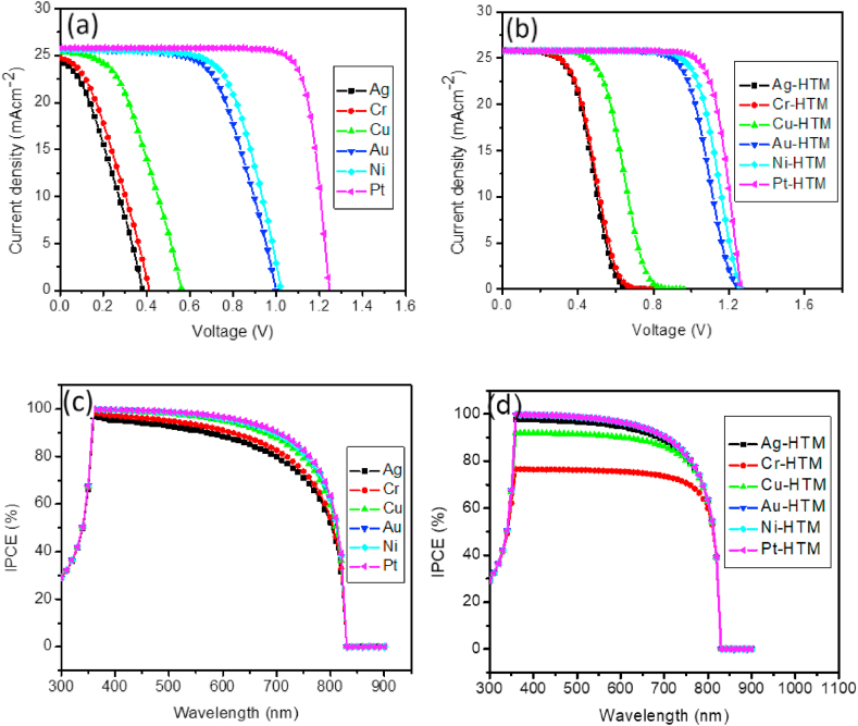
In perovskite solar cells, the metal work function of right contact is a crucial and fundamental factor for built-in voltage (Vbi). Different work functions of metal electrode are expected to give different performances. As such, it must be carefully chosen for device's optimum performance. In this sub-section, the simulation of HTM and HTM-free PSC was done with different metals (Ag, Cr, Cu, Au, Ni and Pt) and their performances were recorded. Fig. 2a & b shows the current-voltage (J-V) behavior of the devices without HTM and with HTM. For both devices, the performance was greatly affected by the type of metal contact used. The metal contact WF ranged between 4.47 and 5.65 eV. Generally, Pt with metal WF of 5.65 eV gave the best performance for both HTM free and HTM-based devices. In terms of the Jsc for HTM-based devices, the impact of BC is negligible for Au, Ni and Pt resulting to constant Jsc values. Fig. 2c & d shows the IPCE against wavelength for the HTM and HTM-free PSCs with different metal contact. The absorption extends throughout the entire visible spectrum and reaches a broad absorption maximum in the 350–820 nm range. The strong absorption at the visible region shows a satisfactory condition of our simulated device under 1sun light and agrees with similar studies with MAPbI3 [24,25]. Table 3, Table 4 show the summary of the obtained results after the simulation. To ascertain the validity of our simulation, the results obtained were compared with experimental works depicted in Table 5 [7]. Since the simulation doesn't account for additional series resistances from BC, FTO, or the reflection of each layer and interface, FF and PCE for the simulated results were higher than experimental values [7]. Additionally, reasonable Jsc and Voc that were in line with experimental findings were obtained, proving the viability of this simulation and illustrating how well the parameter corresponds to that of real devices. Another possible reason for the slight disparity in results is the method of preparation and deposition of the films [7,28,29]. According to some studies, CH3NH3PbI3 is being investigated as an n-type semiconductor [30], while others reported CH3NH3PbI3 as a p-type semiconductor [[31], [32], [33], [34], [35]]. By Yin et al. [36], It was shown that CH3NH3PbI3 had shallow levels that determined the semiconductor type (p or n), as well as p-type vacancies connected to Pb and n-type vacancies connected to CH3NH3+. We can hypothesize that high energy loss occurs during hole transfer to various metal back contacts after metal deposition on CH3NH3PbI3 film or spiro-OMeTAD film as a result of the energy offset between CH3NH3PbI3's valence band edge and the system's Fermi level, which is thought to be one of the main causes of the significant discrepancy between the experimental and simulated results. Miller et al. [37] have demonstrated that the preparation technique affects the work function of the perovskite layer. Surface contamination and the method of measurement are additional factors [7]. This leads to the conclusion that the CH3NH3PbI3 layer's charge carrier density is low in their experimental work and that under the impact of that underlayer's carrier density, the work function changes depending on the preparation and deposition processes. This by implication means that CH3NH3PbI3 practically behaves like an intrinsic semiconductor.
Fig. 2.
(a) J-V curve with different metal contact under illumination without HTM, (b) J-V curve with different metal contact under illumination with HTM, (c) QE with respect to wavelength for HTM-free PSC and (d) QE with respect to wavelength for HTM-based PSC.
Table 3.
J-V characteristic parameters with different metal contact for HTM-free PSC.
| Metal | PCE (%) | FF (%) | Jsc (mA/cm2) | Voc (V) |
|---|---|---|---|---|
| Ag | 3.108 | 33.201 | 24.513 | 0.382 |
| Cr | 3.586 | 35.098 | 24.799 | 0.412 |
| Cu | 6.338 | 44.501 | 25.347 | 0.562 |
| Au | 16.166 | 63.152 | 25.618 | 0.999 |
| Ni | 17.311 | 65.984 | 25.629 | 1.024 |
| Pt | 26.229 | 81.596 | 25.781 | 1.247 |
Table 4.
J-V characteristic parameters with different metal contact for HTM-based PSC.
| Metal | PCE (%) | FF (%) | Jsc (mA/cm2) | Voc (V) |
|---|---|---|---|---|
| Ag-HTM | 8.527 | 42.694 | 25.774 | 0.775 |
| Cr-HTM | 8.630 | 42.193 | 25.774 | 0.794 |
| Cu-HTM | 12.054 | 49.626 | 25.781 | 0.942 |
| Au-HTM | 22.768 | 69.908 | 25.782 | 1.263 |
| Ni-HTM | 23.941 | 73.491 | 25.782 | 1.264 |
| Pt-HTM | 25.608 | 78.601 | 25.782 | 1.264 |
Table 5.
J-V characteristic parameters of HTM-free and HTM-based PSC [7].
| Sample | Jsc (mA/cm2) | Voc (V) | FF (%) | PCE (%) |
|---|---|---|---|---|
| Au Ag |
4.85 4.93 |
0.809 0.087 |
65.38 39.34 |
2.46 0.17 |
| Pt | 7.17 | 0.686 | 62.60 | 3.08 |
| Ni | 8.52 | 0.411 | 49.92 | 1.75 |
| Cu | 10.42 | 0.301 | 33.69 | 1.06 |
| Cr | 0.89 | 0.753 | 21.83 | 0.14 |
| Au-HTM | 20.99 | 1.0091 | 77.60 | 16.44 |
| Ag-HTM | 20.60 | 1.023 | 78.32 | 16.51 |
| Pt-HTM | 20.58 | 1.006 | 71.07 | 14.72 |
| Ni-HTM | 18.21 | 0.834 | 51.61 | 7.83 |
| Cu-HTM | 20.32 | 0.942 | 47.89 | 9.17 |
| Cr-HTM | 0.47 | 0.04 | 18.41 | 0.04 |
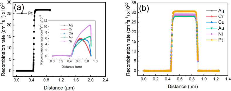
The recombination rate at the interface of metal (Ag, Cr, Cu, Au, and Ni) and spiro-OMeTAD was higher than the recombination rate at the interface of metal (Ag, Cr, Cu, Au, and Ni) and CH3NH3PbI3 which can be depicted in Fig. 3a and b. For Pt, the internal resistance is substantially larger when HTM is inserted than when it is not. This has proven that the spiro-OMeTAD and Pt metal electrodes have significant interfacial resistances, which leads to formation of non-ohmic contact. Using Mo metal contact on spiro-OMeTAD with a work function of 4.6 eV has been demonstrated to cause the contact metal atoms to penetrate the spiro-OMeTAD layer and produce non-ohmic contact with CH3NH3PbI3, which increases series resistance and results in an S-shaped J-V curve [38]. We can clearly detect the S-shape J-V curve in our data in Fig. 2b for Cu since it has the same work function of 4.6 eV and close values of work function for Cr and Ag in the current study. This behavior can be attributed to the penetration of Cu, Cr and Ag atoms through the HTM. It can now be concluded that the spiro-OMeTAD used in our simulation is not a good hole transport material when Cu, Cr and Ag are used as metal contact.
Fig. 3.
The recombination rate of PSC with different metal back contact based on (a) HTM-free and (b) HTM-based device.
It can further be confirmed from the IPCE against wavelength plot for the HTM based devices with Cu, Cr and Ag as metal contact that their quantum efficiencies were below 100% with Cr having 76%, Cu having 92.04% and Ag having 98.07%. In the case of the HTM-free devices, the quantum efficiencies were enhanced with spiro-OMeTAD elimination resulting to IPCE value of 97.08, 98.01 and 99% for Ag, Cr and Cu.
Having obtained the optimal back contact to be Pt with WF of 5.65 eV, we focus on optimizing the thickness of the absorber, ETM thickness, the interface defect between the absorber and the ETM for HTM-free and the interface defect between the absorber and ETM, and between the absorber and HTM for HTM-based.
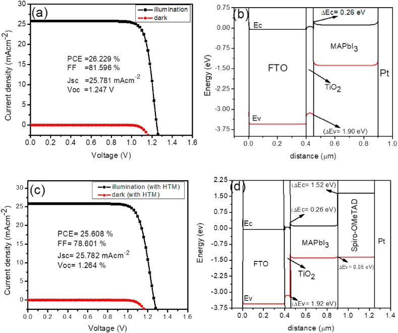
Fig. 4a & b shows the best HTM-free device and its corresponding energy profile. The energy profile demonstrates the effective role of the WF of the metal contact. The photogenerated electrons and holes that are generated in the conduction band with offset (0.26 eV) and the valence band with offset (1.90 eV) are highly beneficial and are expected to allow or/block the careers respectively. TiO2 has a conduction band energy of ∼ −4.0 eV and a deep valence band energy of about −7.3 eV which makes it an ideal material for electron selectivity in PSCs [7,32]. In this scenario, it is anticipated that the metal contact will capture photo-generated holes.
Fig. 4.
(a) J-V curve for optimal metal contact without HTM in the light and the dark, (b) Energy profile diagram of the device with optimal metal contact without HTM, (c) J-V curve in the light and the dark for optimal metal contact with HTM and (d) Device energy profile diagram with optimal metal contact with HTM.
With the insertion of HTM (spiro-OMeTAD), the HOMO of the HTM collects the holes and a relatively high Voc is maintained due to the increase in the built in voltage caused by the insertion. Hence, deeper HOMO results in larger Voc [39]. Thus, the HTM is essential in maintaining a high Voc; consequently, the FF increases significantly to complement the high Voc as shown in Table 3. In a practical term, the HTM is capable of preventing short circuiting in PSC by forming a shell layer between the absorber nanocrystals and the metal [40].
Fig. 4c shows the J-V curve for an HTM device with a different back contact while Fig. 4d shows the energy band gap profile of the HTM-based device. The MAPbI3/Spiro-OMeTAD has a valence band offset (VBO) of 0.05 eV. A barrier in the passage of photo-generated holes from MAPbI3 to HTM results from a larger value of VBO. Because the VBO in this work was so low, spiro-OMeTAD was a good choice for the HTM with Pt metal contact. The VBO value needs to be low to allow holes from the MAPbI3 to enter the HTM, and it shouldn't be high enough to generate an accumulation of holes at the absorber/HTM interface that may trigger recombination [41]. As a result, it's critical to take into account a material with a low negative or value VBO for improved band alignment, which will ultimately lead to improved device performance. The metric parameters for the Pt-metal device with HTM gave Voc = 1.264 V, Jsc = 25.782 mA/cm2, FF = 78.601%, and PCE = 25.608%.
3.2. Influence of absorber thickness in devices with and without HTM
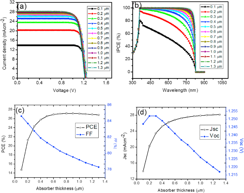
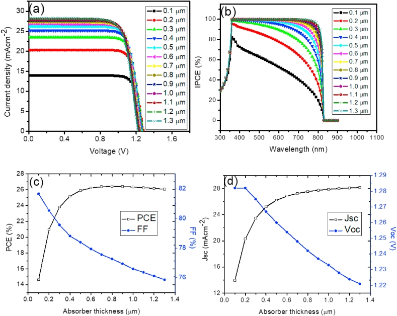
The performance properties of PSCs are significantly influenced by the thickness of MAPbI3. The thickness needs to be chosen in such a way that it will not be too thick no thin. The diffusion lengths and lifetime of photogenerated careers are affected by absorber layer thickness [42]. A simulation was run with an absorber layer thickness range of 0.1–1.3 μm to better understand the impact of perovskite thickness on the metrics of perovskite solar cells. For both HTM-free and HTM-based devices, Fig. 5, Fig. 6a–d display the J-V characteristic curve, IPCE vs. wavelength plots, and variation of the metric parameters with absorber layer thickness. The variation of metric parameters with different thickness values are shown in Fig. 5, Fig. 6c & d. As shown in Fig. 5, Fig. 6a, increase in the perovskite thickness from 0.1 to 0.8 μm results to rapid increase in PCE from 14.718 to 27.154% for HTM-free and from 14.630 to 26.436% for HTM-based. Beyond 0.8 μm, there was a decrease in PCE. The Voc and Jsc increases rapidly with increase in absorber thickness for both configurations. FF drastically decreases at the same time to counterbalance the high Voc and Jsc, bringing about slightly higher PCE. The enhanced increase in PCE up to 0.8 μm is attributed to a high absorption coefficient of the devices observed in this range of spectrum [25]. Therefore, the optimal thickness of the MAPbI3 in our research work was 0.8 μm and as such considered for further simulation. The device performance for the HTM-free at that optimal value is as follows: PCE = 27.154%, FF = 79.910%, Jsc = 27.546 mA/cm2, and Voc = 1.234 V (Table 6) and for the device performance for the HTM-based is as follows: PCE = 26.436%. FF = 77.267%, Jsc = 27.546 mA/cm2, and Voc = 1.242 V (Table 7).
Fig. 5.
(a) J-V curve with varying thickness of absorber in the light condition, (b) QE vs. wavelength, (c) PCE and FF vs. thickness of absorber and (d) Jsc and Voc vs. absorber thickness for PSCs without HTM.
Fig. 6.
(a) J-V curve with varying thickness of absorber in the light condition, (b) QE vs. wavelength, (c) PCE and FF vs. thickness of absorber and (d) Jsc and Voc vs. absorber thickness for PSCs with HTM.
Table 6.
J-V characteristic data without HTM with varying absorber thickness.
| Thickness (μm) | PCE (%) | FF (%) | Jsc (mAcm−2) | Voc (V) |
|---|---|---|---|---|
| 0.1 | 14.718 | 84.617 | 13.950 | 1.247 |
| 0.2 | 21.278 | 83.711 | 20.296 | 1.252 |
| 0.3 | 24.327 | 82.777 | 23.482 | 1.252 |
| 0.4 | 25.786 | 81.907 | 25.213 | 1.249 |
| 0.5 | 26.552 | 81.331 | 26.223 | 1.245 |
| 0.6 | 26.930 | 80.816 | 26.851 | 1.241 |
| 0.7 | 27.085 | 80.293 | 27.263 | 1.237 |
| 0.8 | 27.154 | 79.910 | 27.546 | 1.234 |
| 0.9 | 27.152 | 79.562 | 27.748 | 1.230 |
| 1.0 | 27.097 | 79.206 | 27.897 | 1.226 |
| 1.1 | 27.004 | 78.840 | 28.010 | 1.223 |
| 1.2 | 26.926 | 78.574 | 28.098 | 1.220 |
| 1.3 | 26.835 | 78.302 | 28.168 | 1.217 |
Table 7.
J-V characteristic data with HTM with varying absorber thickness.
| Thickness (μm) | PCE (%) | FF (%) | Jsc (mA/cm2) | Voc (V) |
|---|---|---|---|---|
| 0.1 | 14.630 | 81.670 | 13.968 | 13.968 |
| 0.2 | 20.952 | 80.530 | 20.302 | 20.302 |
| 0.3 | 23.821 | 79.563 | 23.485 | 23.485 |
| 0.4 | 25.185 | 78.815 | 25.214 | 25.214 |
| 0.5 | 25.903 | 78.389 | 26.224 | 26.224 |
| 0.6 | 26.236 | 77.940 | 26.851 | 26.851 |
| 0.7 | 26.381 | 77.559 | 27.263 | 27.263 |
| 0.8 | 26.436 | 77.267 | 27.546 | 27.546 |
| 0.9 | 26.412 | 76.942 | 27.748 | 27.748 |
| 1.0 | 26.338 | 76.595 | 27.897 | 27.897 |
| 1.1 | 26.271 | 76.358 | 28.010 | 28.010 |
| 1.2 | 26.185 | 76.116 | 28.098 | 28.098 |
| 1.3 | 26.082 | 75.858 | 28.168 | 28.168 |
From the results, it shows that the elimination of the HTM was slightly beneficial to the efficiency enhancement. To support this statement, in practical terms, it was demonstrated that after depositing Au metal contact on MAPbI3 film, the energy offset between valence band edge of MAPbI3 and the Fermi level of the system was found to be 0.6 eV which leads to low energy loss during the process of transferring hole to the metal right contact (Au) [7]. Thus, irrespective of the existence of HTM or not, the choice of the absorber thickness is crucial in realizing high PCE.
The IPCE against wavelength curves for both devices with HTM and without HTM shows increase in quantum efficiencies with increase in the absorber thickness. The QE increases from 80% at (0.1 μm) to 100% at (1.3 μm). The strong QE is due to increase in extinction coefficient as the thickness increases.
3.3. ETL/absorber interface defect for HTM-free
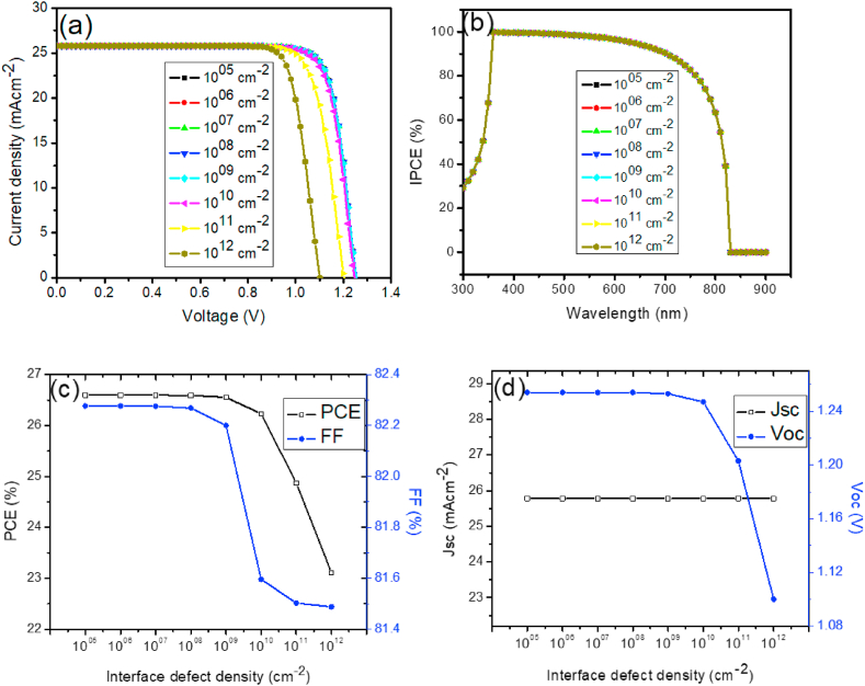
The ETL/absorber interface flaw adversely affects the PSC device's performance. To examine the performance of PSC in a more realistic way, ETL/absorber interface density (Nt) was introduced in our initial device ranging from 1005 to 1012 cm−2, attempt to exceed above 1012 cm−2 leads to convergence failure. Though the values chosen are somewhat too low in practical terms but it's necessary to elucidate its significance in theoretical basis. At the ETL/absorber interface, the Nt affects the stability and performance properties of PSCs. Fig. 7a–d shows the J-V characteristics plot, IPCE-wavelength plot and variation in device parameters with diverse defect densities of ETL/absorber interface, PCE and FF maintains a constant value at 1005 and 1006 cm−2 before they start decreasing. The Voc also maintains a linear variation up to 1008 cm−2 before it starts decreasing. The drop in device characteristics may be explained by the fact that electrons moving from the MAPbI3 layer to TiO2 are more likely to be trapped or quenched as a result of recombination as the Nt at the ETL/absorber interface increases. Though there are three defect density (1005, 1006, and 1007 cm−2) with the same performance as shown in Table 8, so ETL/absorber defect density of a value equal to or less than 1007 cm−2 gives reasonable performance. But it is often impractical to realize a very low ETL/absorber defect, so we chose 1007 cm−2 as optimized value for further simulations. The performance of the device at 1007 cm−2 ETL/absorber defect density is as follows: Voc = 1.254 V, Jsc = 25.781 mA/cm2, FF = 82.277% and PCE = 26.596%.
Fig. 7.
(a) J-V curve with varying ETL/absorber interface defect density in the light condition, (b) QE vs. wavelength, (c) PCE and FF vs. ETL/absorber interface defect density and (d) Jsc and Voc vs. ETL/absorber interface defect density for PSCs without HTM.
Table 8.
J-V characteristic data without HTM with varying ETL/absorber interface defect density.
| Nt (cm−2) | PCE (%) | FF (%) | Jsc (mAcm−2) | Voc (V) |
|---|---|---|---|---|
| 1005 | 26.596 | 82.277 | 25.781 | 1.254 |
| 1006 | 26.596 | 82.277 | 25.781 | 1.254 |
| 1007 | 26.596 | 82.276 | 25.781 | 1.254 |
| 1008 | 26.592 | 82.269 | 25.781 | 1.254 |
| 1009 | 26.556 | 82.200 | 25.781 | 1.253 |
| 1010 | 26.229 | 81.596 | 25.781 | 1.247 |
| 1011 | 24.868 | 81.503 | 25.781 | 1.203 |
| 1012 | 23.109 | 81.488 | 25.781 | 1.100 |
3.4. ETL/absorber interface defect and HTM/absorber interface defect for HTM-base
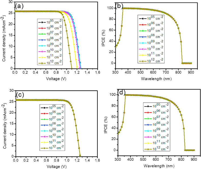
The ETL/absorber interface flaw significantly affects the PSC device performance. To examine the performance of PSC in a more realistic way, ETL/absorber interface density was introduced in our initial device with variation values from 1005 to 1012 cm−2. At the ETL/absorber interface, the Nt affects the stability and performance properties of PSCs with HTM since the structures are also made up of discontinues materials. Fig. 8a–d shows the J-V characteristics plot, IPCE-wavelength plot with diverse ETL/absorber interface defect densities, J-V characteristics plot of absorber/HTM interface defect densities and IPCE-wavelength plot with absorber/HTM interface defect densities. PCE and FF maintains a constant value at 1005 and 1006 cm−2 before they start decreasing. The Voc also maintains a linear variation up to 1008 cm−2 before it starts decreasing. The drop in device characteristics may be explained by the fact that electrons moving from the MAPbI3 layer to the ETL are more likely to be caught or quenched as a result of recombination as the Nt at the ETL/absorber interface increases. Despite the fact that three ETL/absorbers have the same performance as shown in Table 9, therefore, a defect density for ETL/absorbers equal to or below 1007 cm−2 results in acceptable performance. However, it is frequently impracticable to achieve a very small ETL or absorber defect, so we chose 1007 cm−2 as optimized value for further simulations. The performance of the device at 1007 cm−2 ETL/absorbers defect density is as follows: Voc = 1.277 V, Jsc = 25.782 mA/cm2, FF = 78.943% and PCE = 25.991%.
Fig. 8.
(a) J-V curve with varying ETL/absorber interface defect density in the light condition, (b) QE vs. wavelength of ETL/absorber interface defect density (c) J-V curve with varying absorber/HTM interface defect density in the light condition and (d) QE vs. wavelength of absorber/HTM interface defect density for PSCs with HTM.
Table 9.
J-V characteristic data with HTM with varying ETL/absorber interface defect density.
| Nt (cm−2) (ETM-Abs) | PCE (%) | FF (%) | Jsc (mA/cm2) | Voc (V) |
|---|---|---|---|---|
| 1005 | 25.991 | 78.943 | 25.782 | 1.277 |
| 1006 | 25.991 | 78.943 | 25.782 | 1.277 |
| 1007 | 25.991 | 78.943 | 25.782 | 1.277 |
| 1008 | 25.986 | 78.939 | 25.782 | 1.277 |
| 1009 | 25.947 | 78.902 | 25.782 | 1.276 |
| 1010 | 25.608 | 78.601 | 25.782 | 1.264 |
| 1011 | 24.216 | 77.922 | 25.782 | 1.205 |
| 1012 | 22.451 | 79.166 | 25.782 | 1.100 |
Additionally, the PSC performance and stability are impacted by the Nt at the absorber/HTM contact. The device was simulated with by changing the absorber/HTM Nt from 1005 to 1012 cm−2. As shown in Fig. 8c and d, varying the defect density at the absorber/HTL interface has no effect on the performance metrics of the device (see Table 10). The IPCE versus wavelength curve exhibits spectral overlap when the absorber/HTL Nt is chosen between 1005 to 1012 cm−2, which is explained by unchanging optical absorption efficiency at the chosen values of the absorber/HTM defect density.
Table 10.
J-V characteristic data with HTM with varying absorber/HTM interface defect density.
| Nt (cm−2) (Abs-HTM) | PCE (%) | FF (%) | Jsc (mA/cm2) | Voc (V) |
|---|---|---|---|---|
| 1005 | 25.608 | 78.601 | 25.782 | 1.264 |
| 1006 | 25.608 | 78.601 | 25.782 | 1.264 |
| 1007 | 25.608 | 78.601 | 25.782 | 1.264 |
| 1008 | 25.608 | 78.601 | 25.782 | 1.264 |
| 1009 | 25.608 | 78.601 | 25.782 | 1.264 |
| 1010 | 25.608 | 78.601 | 25.782 | 1.264 |
| 1011 | 25.608 | 78.601 | 25.782 | 1.264 |
| 1012 | 25.608 | 78.601 | 25.782 | 1.264 |
3.5. ETM thickness with and without HTM
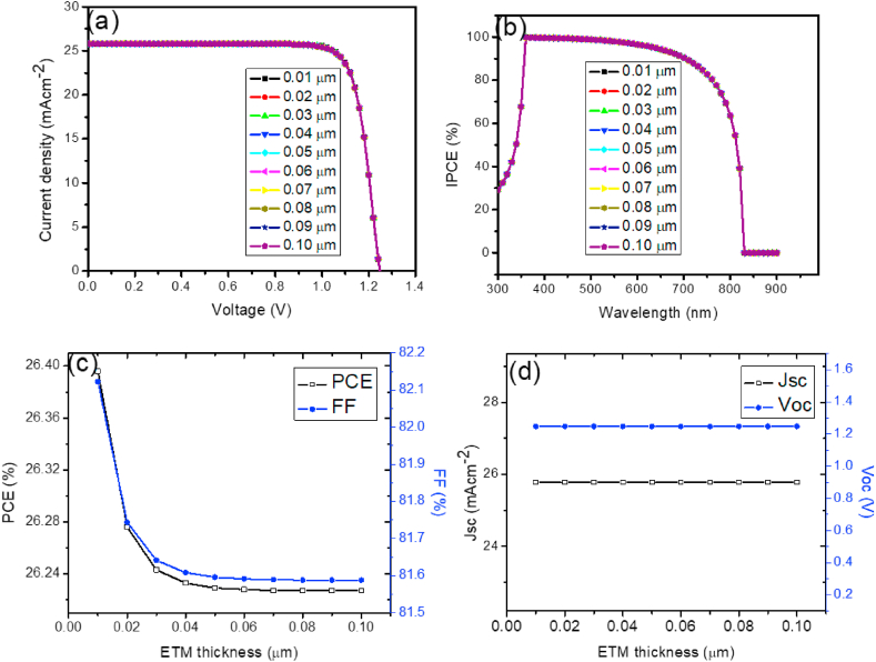
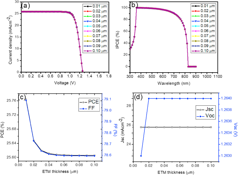
In order to examine how performance is impacted by ETL thickness of PSCs with HTM and without HTM, the thickness of the ETL was varied from 0.01 to 0.10 μm. Fig. 9, Fig. 10d show the J-V curves, IPCE-wavelength, and photovoltaic parameters with respect to the varied thickness on device without HTM and with HTM. With ETL thickness increased, the Jsc and Voc were unaffected. The PCE and FF slightly decreases with increased thickness. The decrease in PCE and FF can be attributed to the series resistance offered by the layer thickness. The QE versus wavelength curve exhibits spectrum overlap when the thickness is chosen between 0.01 and 0.10 μm, which is explained by the unchanged optical absorption efficiency for the chosen thickness values. The optimal ETL thickness was 0.01 μm for both HTM-free and HTM-based devices. The parameters at the optimal values are as follows: (PCE = 26.396%, FF = 82.123%, Jsc = 25.781 mA/cm2 and Voc = 1.247 V) (Table 11) for device without HTM and (PCE = 25.764%, FF = 79.091%, Jsc = 25.782 mA/cm2 and Voc = 1.263 V) (Table 12) for device with HTM.
Fig. 9.
(a) J-V curve with varying ETL thickness in the light condition, (b) QE vs. wavelength, (c) PCE and FF vs. ETL thickness and (d) Jsc and Voc vs. ETL thickness for PSCs without HTM.
Fig. 10.
(a) J-V curve with varying ETL thickness in the light condition, (b) QE vs. wavelength, (c) PCE and FF vs. ETL thickness and (d) Jsc and Voc vs. ETL thickness for PSCs with HTM.
Table 11.
J-V characteristic data without HTM with varying ETL thickness.
| Thickness (μm) | PCE (%) | FF (%) | Jsc (mA/cm2) | Voc (V) |
|---|---|---|---|---|
| 0.01 | 26.396 | 82.123 | 25.781 | 1.247 |
| 0.02 | 26.276 | 81.744 | 25.781 | 1.247 |
| 0.03 | 26.243 | 81.641 | 25.781 | 1.247 |
| 0.04 | 26.233 | 81.608 | 25.781 | 1.247 |
| 0.05 | 26.229 | 81.596 | 25.781 | 1.247 |
| 0.06 | 26.228 | 81.591 | 25.781 | 1.247 |
| 0.07 | 26.227 | 81.589 | 25.781 | 1.247 |
| 0.08 | 26.227 | 81.588 | 25.781 | 1.247 |
| 0.09 | 26.227 | 81.588 | 25.781 | 1.247 |
| 0.10 | 26.227 | 81.588 | 25.781 | 1.247 |
Table 12.
J-V characteristic data with HTM with varying ETL thickness.
| Thickness (μm) | PCE (%) | FF (%) | Jsc (mA/cm2) | Voc (V) |
|---|---|---|---|---|
| 0.01 | 25.764 | 79.091 | 25.782 | 1.263 |
| 0.02 | 25.648 | 78.729 | 25.782 | 1.264 |
| 0.03 | 25.62 | 78.639 | 25.782 | 1.264 |
| 0.04 | 25.611 | 78.611 | 25.782 | 1.264 |
| 0.05 | 25.608 | 78.601 | 25.782 | 1.264 |
| 0.06 | 25.607 | 78.597 | 25.782 | 1.264 |
| 0.07 | 25.606 | 78.596 | 25.782 | 1.264 |
| 0.08 | 25.606 | 78.596 | 25.782 | 1.264 |
| 0.09 | 25.606 | 78.595 | 25.782 | 1.264 |
| 0.10 | 25.606 | 78.595 | 25.782 | 1.264 |
3.6. Optimized device
After careful variation of the selected ranged parameters, we obtained 0.8 μm for MAPbI3 thickness for both devices without HTM and with HTM, 1007 cm−2 for TiO2/MAPbI3 interface defect density for both devices without HTM and with HTM, 1007 cm−2 MAPbI3/HTM interface defect density for device with HTM, 0.01 μm for TiO2 thickness for both devices without HTM and with HTM. The optimized parameters were used to simulate the final device with and without HTM.
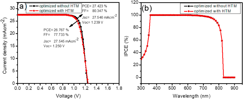
Fig. 11 depicts the J-V characteristics and IPCE-wavelength curve for the optimized device with and without HTM. The performance of both devices gave optimal parameters as follows: Voc = 1.239 V, Jsc = 27.546 mA/cm2, FF = 80.347% and PCE = 27.423% for device without HTM and Voc = 1.250 V, Jsc = 27.545 mA/cm2, FF = 77.733% and PCE = 26.767% for device with HTM.
Fig. 11.
(a) Optimized J–V curves for HTM and HTM-free PSC and (b) IPCE with respect to wavelength for HTM and HTM-free PSC.
The outcomes suggest an outstanding improvement of ∼1.05 and ∼1.07 times in PCE and Jsc over the unoptimized cell without HTM, and ∼1.05 and ∼1.07 times in PCE and Jsc against the unoptimized cell with HTM. Both devices experienced the same enhancement strength. Thus, irrespective of whether there is HTM or not, the enhancement power remains same.
Table 13 shows the comparison of results obtained in this study via simulation with other previously published works to validate our findings and its applicability in research. The results obtained are encouraging and have highlighted the prospect of the proposed structure and emphasize the importance of using HTM-free solar cells without deteriorating the efficiency.
Table 13.
J-V characteristic data of experimental and simulated results.
| Device | PCE (%) | FF (%) | Jsc (mA/cm2) | Voc (V) | Remark |
|---|---|---|---|---|---|
| Simulation with HTM | 26.767 | 77.733 | 27.545 | 1.250 | This work |
| Simulation without HTM | 27.423 | 80.347 | 27.546 | 1.239 | This work |
| Experimental with HTM | 16.510 | 78.32 | 20.600 | 1.023 | [7] |
| Simulation without HTM | 25.750 | 89.500 | 23.250 | 1.240 | [25] |
| Simulation with HTM | 23.040 | 81.680 | 24.980 | 1.120 | [43] |
| Simulation with HTM | 26.667 | 83.005 | 23.232 | 1.383 | [44] |
| Simulation without HTM | 15.020 | 82.830 | 24.740 | 0.730 | [45] |
| Experimental without HTM | 15.040 | 61.570 | 23.090 | 1.058 | [46] |
4. Conclusion
In this present work, the impact of metal contact on HTM and HTM-free PSC was first studied to obtain the optimal work function. With the control of thickness of absorber layer (0.1–1.3 μm), interface defect density from 1005 - 1012 cm−2, and ETM thickness from 0.01 to 0.10 μm for both HTM and HTM-free perovskite solar cells, their effects were investigated through optimization to obtain the final optimized devices using SCAPS-1D simulation tool. The optimized device without HTM revealed the efficiency of power conversion of 27.423%, with 80.347% of fill factor, current density of 27.546 mA/cm2, voltage of 1.239 V and maximum quantum efficiency of 100% in the visible range whereas the device with HTM demonstrated a power conversion efficiency of 26.767%, fill factor of 77.733%, current density of 27.545 mA/cm2, voltage of 1.250 V and also a maximum incident to photon conversion efficiency of 100% in the visible region. These results show an improvement of ∼1.05 and ∼1.07 times in PCE and Jsc over the unoptimized cells with and without HTM. The results obtained are impressive and have demonstrated the prospect of alternative metal back contact other than Au and have indicated the possibility of efficiency enhancement on simplified structures.
Funding
This article did not receive any funding support.
Author contribution statement
Eli Danladi: conceived and designed the experiments; performed the experiments; analyzed and interpreted the data; contributed reagents, materials, analysis tools or data; wrote the paper.
Philibus M. Gyuk: performed the experiments; analyzed and interpreted the data; contributed reagents, materials, analysis tools or data.
Nicholas N. Tasie: conceived and designed the experiments; analyzed and interpreted the data; contributed reagents, materials, analysis tools or data.
Anselem C. Egbugha; Debidatta Behera; Ismail Hossain; Ibrahim M. Bagudo; Mohammad L. Madugu; Jonathan T. Ikyumbur: analyzed and interpreted the data; contributed reagents, materials, analysis tools or data.
Data availability statement
Data will be made available on request.
Declaration of competing interest
Authors have declared that there was no conflict of interest.
Acknowledgement
The SCAPS software package was created and made available for use by Professor Marc Burgelman and his team at the Department of Electronics and Information Systems at the University of Ghent in Belgium, for which the authors are grateful.
References
- 1.Moodley P. Sustainable Biofuels: opportunities and challenges. Appl. Biotechnol. Rev. 2021:1–20. doi: 10.1016/B978-0-12-820297-5.00003-7. [DOI] [Google Scholar]
- 2.Jun H.K., Careem M.A., Arof A.K. Quantum dot-sensitized solar cells perspective and recent developments: a review of Cd chalcogenide quantum dots as sensitizers. Renew. Sustain. Energy Rev. 2013;22:148–167. doi: 10.1016/j.rser.2013.01.030. [DOI] [Google Scholar]
- 3.Gratzel M. Photovoltaic and photoelectrochemical conversion of solar energy. Philos. Trans. Royal Soc. A. 2007;365:993–1005. doi: 10.1098/rsta.2006.1963. [DOI] [PubMed] [Google Scholar]
- 4.F Ibitoye I. The millennium development goals and household energy requirements in Nigeria. SpringerPlus. 2013;2:529. doi: 10.1186/2193-1801-2-529. [DOI] [PMC free article] [PubMed] [Google Scholar]
- 5.Danladi E., Kashif M., Ichoja A., Ayiya B.B. Modeling of a Sn-based HTM-free perovskite solar cell using one dimensional solar cell capacitance simulator tool. Trans. Tianjin Univ. 2023;29:62–72. doi: 10.1007/s12209-022-00343-w. [DOI] [Google Scholar]
- 6.Zadeh N.J., Zarandi M.B., Nateghi M.R. Optical properties of the perovskite films deposited on meso-porous TiO2 by one step and hot casting techniques. Thin Solid Films. 2019;671:139–146. doi: 10.1016/j.tsf.2018.12.029. [DOI] [Google Scholar]
- 7.Behrouznejad F., Shahbazi S., Taghavinia N., Wu H.P., Diau E.W.G. A study on utilizing different metals as the back contact of CH3NH3PbI3 perovskite solar cells, Journal of materials chemistry A 4 (2016) J. Mater. Chem. 2016;4:13488–13498. doi: 10.1039/C6TA05938D. [DOI] [Google Scholar]
- 8.Kojima A., Teshima K., Shirai Y., Miyasaka T. Organometal halide perovskites as visible-light sensitizers for photovoltaic cells. J. Am. Chem. Soc. 2009;131(17):6050–6051. doi: 10.1021/ja809598r. [DOI] [PubMed] [Google Scholar]
- 9.Qu Z., Ma F., Zhao Y., Chu X., Yu S., You J. Updated progresses in perovskite solar cells, chin. Phys. Lett. 2021;38 doi: 10.1088/0256-307X/38/10/107801. [DOI] [Google Scholar]
- 10.Raza E., Ahmad Z., Asif M., Aziz F., Riaz K., Mehmood M.Q., Bhadra J., Al-Thani N.J. Numerical modelling and performance optimization of carbon-based hole transport layer free perovskite solar cells. Opt. Mater. 2022;125 doi: 10.1016/j.optmat.2022.112075. [DOI] [Google Scholar]
- 11.Pitchaiya S., Eswaramoorthy N., Natarajan M., Santhanam A., Asokan V., Ramakrishnan V.M., Rangasamy B., Sundaram S., Ravirajan P., Velauthapilla D. Perovskite solar cells: a porous graphitic carbon based hole transporter/counter electrode material extracted from an invasive plant species Eichhornia crassipes. Sci. Rep. 2020;10:6835. doi: 10.1038/s41598-020-62900-4. [DOI] [PMC free article] [PubMed] [Google Scholar]
- 12.Bogachuk D., Yang B., Suo J J., Martineau D., Verma A., Narbey S., Anaya M., Frohna K., Doherty T., Müller D., Herterich J.P., Zouhair S., Hagfeldt A., Stranks S.D., Würfel U., Hinsch A., Wagner L. Perovskite solar cells with carbon-based electrodes–quantification of losses and strategies to overcome them. Adv. Energy Mater. 2022;12 doi: 10.1002/aenm.202103128. [DOI] [Google Scholar]
- 13.Rong X., Tian H., Bi W., Jin H., Zhang T., Guo D., Zhao K. Impact of metal electrode work function of CH3NH3PbI3/p-Si planar heterojunction perovskite solar cells. Sol. Energy. 2017;158:424–431. doi: 10.1016/j.solener.2017.08.050. [DOI] [Google Scholar]
- 14.Zhang W., Xiong J., Wang S., Liu W., Li J., Wang D., Gu H., Wang X., Li J. Highly conductive and transparent silver grid/metal oxide hybrid electrodes for low temperature planar perovskite solar cells. J. Power Sources. 2017;337:118–124. doi: 10.1016/j.jpowsour.2016.10.101. [DOI] [Google Scholar]
- 15.Wang L., Li G.R., Zhao Q., Gao X.P. Non-precious transition metals as counter electrode of perovskite solar cells. Energy Storage Mater. 2016;7:40–47. doi: 10.1016/j.ensm.2016.11.007. [DOI] [Google Scholar]
- 16.Xie X., Liu G., Xu C., Li S., Liu Z., Lee E.C. Tuning the work function of indiumtin-oxide electrodes for low-temperature-processed, titanium-oxide-free perovskite solar cells. Org. Electron. 2017;44:120–125. doi: 10.1016/j.orgel.2017.02.011. [DOI] [Google Scholar]
- 17.Chen M., Zha R.H., Yuan Z.Y., Jing Q.S., Huang Z.Y., Yang X.K., Yang S.M., Zhao X.H., Xu D.L., Zou G.D. Boron and phosphorus co-doped carbon counter electrode for efficient hole-conductor-free perovskite solar cell. Chem. Eng. J. 2017;313:791–800. doi: 10.1016/j.cej.2016.12.050. [DOI] [Google Scholar]
- 18.Domanski K., Correa-Baena J.P., Mine N., Nazeeruddin M.K., Abate A., Saliba M., Tress W., Hagfeldt A., Grätzel M. Not all that glitters is gold: metal-migration-induced degradation in perovskite solar cells. ACS Nano. 2016;10:6306–6314. doi: 10.1021/acsnano.6b02613. [DOI] [PubMed] [Google Scholar]
- 19.Rahighi R., Gholipour S., Amin M.A., Ansari M.Z. Hole-transport material engineering in highly durable carbon-based perovskite photovoltaic devices. Nanomaterials. 2023;13:1417. doi: 10.3390/nano13081417. [DOI] [PMC free article] [PubMed] [Google Scholar]
- 20.Feng L., Zhu J., Wei J., Li Y., Lv M., Yang S., Zhang B., Yao J., Dai S. Numerical simulation: toward the design of high-efficiency planar perovskite solar cells. Appl. Phys. Lett. 2014;104 doi: 10.1063/1.4885367. [DOI] [Google Scholar]
- 21.Fakhri N., Salay N.M., Gholami F.S., SaeidNahaei S., Park S.N., Rhee S.B. Simulation of perovskite solar cells optimized by the inverse planar method in SILVACO: 3D electrical and optical models. Energies. 2021;14:5944. doi: 10.3390/en14185944. [DOI] [Google Scholar]
- 22.Zandi S., Saxena P., Gorji N.E. Numerical simulation of heat distribution in RGO-contacted perovskite solar cells using COMSOL. Sol. Energy. 2020;197:105–110. doi: 10.1016/j.solener.2019.12.050. [DOI] [Google Scholar]
- 23.Danladi E., Salawu A.O., Abdulmalik M.O., Onoja E.D., Onwoke E.E., Adepehin D.S. Optimization of absorber and ETM layer thickness for enhanced tin based perovskite solar cell performance using SCAPS-1D software. PHYSICS Access. 2022;2(1):1–11. doi: 10.47514/phyaccess.2022.2.1.001. [DOI] [Google Scholar]
- 24.Minemoto T., Murata M. Impact of work function of back contact of perovskite solar cells without hole transport material analyzed by device simulation. Curr. Appl. Phys. 2014;14(11):1428–1433. doi: 10.1016/j.cap.2014.08.002. [DOI] [Google Scholar]
- 25.Danladi E., Shuaibu A., Ahmad M.S., Tasiu J. Numerical modeling and analysis of HTM-free heterojunction solar cell using SCAPS-1D. East Eur. J. Phys. 2021;2:135–145. doi: 10.26565/2312-4334-2021-2-11. [DOI] [Google Scholar]
- 26.Danladi E., Onimisi M.Y., Garba S., Ugbe R.U., Owolabi J.A., Ige O.O., Ibeh G.J., Muhammed A.O. Simulation and optimization of lead-based perovskite solar cells with cuprous oxide as a p-type inorganic layer. Journal of the Nigerian Society of Physical Sciences. 2019;1(1):72–81. doi: 10.46481/jnsps.2019.13. [DOI] [Google Scholar]
- 27.Tiwari P., Alotaibi M.F., Al-Hadeethi Y., Srivastava V., Arkook B., Sadanand, Lohia P., Dwivedi D.K., Umar A., Algadi H., Bascoutas S. Design and simulation of efficient SnS-based solar cell using spiro-OMeTAD as hole transport layer. Nanomaterials. 2022;12:2506. doi: 10.3390/nano12142506. [DOI] [PMC free article] [PubMed] [Google Scholar]
- 28.Liu M., Johnston M.B., Snaith H.J. Efficient planar heterojunction perovskite solar cells by vapour deposition. Nature. 2013;501:395–398. doi: 10.1038/nature12509. [DOI] [PubMed] [Google Scholar]
- 29.Liu D., Kelly T.L. Perovskite solar cells with a planar heterojunction structure prepared using room –temperature solution processing techniques. Nature Photon. 2013;8:133–138. doi: 10.1038/nphoton.2013.342. [DOI] [Google Scholar]
- 30.Liu X., Wang C., Lyu L., Wang C., Xiao Z., Bi C., Huang J., Gao Y. Electronic structures at the interface between Au and CH3NH3PbI3. Phys. Chem. Chem. Phys. 2015;17:896–902. doi: 10.1039/C4CP03842H. [DOI] [PubMed] [Google Scholar]
- 31.Zhang F., Yang X., Wang H., Cheng M., Zhao J., Sun L. Structure engineering of hole-conductor free perovskite based solar cells with low-temperature-processed commercial carbon paste as cathode. ACS Appl. Mater. Interfaces. 2014;6(8):16140–16146. doi: 10.1021/am504175x. [DOI] [PubMed] [Google Scholar]
- 32.Etgar L., Gao P., Xue Z.S., Peng Q., Chandiran A.K., Liu B., Nazeeruddin M.K., Gratzel M. Mesoscopic CH3NH3PbI3/TiO2 heterojunction solar cells. J. Am. Chem. Soc. 2012;134(42):17396–17399. doi: 10.1021/ja307789s. [DOI] [PubMed] [Google Scholar]
- 33.Laban W.A., Etgar L. Depleted hole conductor-free lead halide iodide heterojunction solar cells. Energy Environ. Sci. 2013;6:3249–3253. doi: 10.1039/C3EE42282H. [DOI] [Google Scholar]
- 34.Gamliel S., Dymshits A., Aharon S., Terkieltaub E., Etgar L. Micrometer sized perovskite crystals in planar hole conductor free solar cells. J. Phys. Chem. C. 2015;119:19722–19728. doi: 10.1021/acs.jpcc.5b07554. [DOI] [Google Scholar]
- 35.Dymshits A., Rotem A., Etgar L. High voltage in hole conductor free organo metal halide perovskite solar cells. J. Mater. Chem. 2014;2:20776–20781. doi: 10.1039/C4TA05613B. [DOI] [Google Scholar]
- 36.Yin W.J., Shi T., Yan Y. Unusual defect physics in CH3NH3PbI3 perovskite solar cell absorber. Appl. Phys. Lett. 2014;104 doi: 10.1063/1.4864778. [DOI] [Google Scholar]
- 37.Miller E.M., Zhao Y., Mercado C.C., Saha S.K., Luther J.M., Zhu K., Stevanovic V., Perkins C.L., de Lagemaat J.V. Substrate-controlled band positions in CH3NH3PbI3 perovskite films. Phys. Chem. Chem. Phys. 2014;16:22122–22130. doi: 10.1039/C4CP03533J. [DOI] [PubMed] [Google Scholar]
- 38.Jeong I., Kim H.J., Lee B.S., Son H.J., Kim J.Y., Lee D.K., Kim D.E., Lee J., Ko M.J. Highly efficient perovskite solar cells on mechanically durable molybdenum cathode. Nano Energy. 2015;17:131–139. doi: 10.1016/j.nanoen.2015.07.025. [DOI] [Google Scholar]
- 39.Ryu S., Noh J.H., Jeon N.J., Kim Y.C., Yang W.S., Seo J., Seok S.I. Voltage output of efficient perovskite solar cells with high open-circuit voltage and fill factor. Energy Environ. Sci. 2014;7:2614–2618. doi: 10.1039/C4EE00762J. [DOI] [Google Scholar]
- 40.Xu Y., Lin Z., Wei W., Hao Y., Liu S., Ouyang J., Chang J. Recent progress of electrode materials for flexible perovskite solar cells. Nano-Micro Lett. 2022;14:117. doi: 10.1007/s40820-022-00859-9. [DOI] [PMC free article] [PubMed] [Google Scholar]
- 41.Pindolia G., Shinde S.M., Jha P.K. Optimization of an inorganic lead free RbGeI3 based perovskite solar cell by SCAPS-1D simulation. Sol. Energy. 2022;236:802–821. doi: 10.1016/j.solener.2022.03.053. [DOI] [Google Scholar]
- 42.Barbé J., Tietze M.L., Neophytou M., Murali B., Alarousu E., Labban A.E., Abulikemu F., Yue W., Mohammed O.F., McCulluch I., Amassian A., Gobbo S.D. Amorphous tin oxide as a low-temperature-processed electrontransport layer for organic and hybrid perovskite solar cells. ACS Appl. Mater. Interfaces. 2017;9:11828–11836. doi: 10.1021/acsami.6b13675. [DOI] [PubMed] [Google Scholar]
- 43.Raoui Y., Ez-Zahraouy H., Tahiri N., El Bounagui O., Ahmad O., Kazim S. Performance analysis of MAPbI3 based perovskite solar cells employing diverse charge selective contacts: simulation study. Sol. Energy. 2019;193:948–955. doi: 10.1016/j.solener.2019.10.009. [DOI] [Google Scholar]
- 44.Danladi E., Egbugha A.C., Obasi R.C., Tasie N.N., Achem C.U., Haruna I.S., Ezeh L.O. Defect and doping concentration study with series and shunt resistance influence on graphene modified perovskite solar cell: a numerical investigation in SCAPS-1D framework. J. Indian Chem. Soc. 2023;100 doi: 10.1016/j.jics.2023.101001. [DOI] [Google Scholar]
- 45.Lin L., Jiang L., Qiu Y., Yu Y. Modeling and analysis of HTM-free perovskite solar cells based on ZnO electron transport layer. Superlattices and Microstruct. 2017;104:167–177. doi: 10.1016/j.spmi.2017.02.028. [DOI] [Google Scholar]
- 46.Zhou J., Ye Z., Hou J., Wu J., Zheng Y.Z., Tao X. (2018). Efficient ambient-air-stable HTM-free carbon-based perovskite solar cells with hybrid 2D-3D lead halide photoabsorber. J. Mater. Chem. 2018;6:22626–22635. doi: 10.1039/C8TA07836J. [DOI] [Google Scholar]
Associated Data
This section collects any data citations, data availability statements, or supplementary materials included in this article.
Data Availability Statement
Data will be made available on request.


