

Abstract
Chalcohalide mixed-anion crystals have seen a rise in interest as “perovskite-inspired materials” with the goal of combining the ambient stability of metal chalcogenides with the exceptional optoelectronic performance of metal halides. Sn2SbS2I3 is a promising candidate, having achieved a photovoltaic power conversion efficiency above 4%. However, there is uncertainty over the crystal structure and physical properties of this crystal family. Using a first-principles cluster expansion approach, we predict a disordered room-temperature structure, comprising both static and dynamic cation disorder on different crystallographic sites. These predictions are confirmed using single-crystal X-ray diffraction. Disorder leads to a lowering of the bandgap from 1.8 eV at low temperature to 1.5 eV at the experimental annealing temperature of 573 K. Cation disorder tailoring the bandgap allows for targeted application or for the use in a graded solar cell, which when combined with material properties associated with defect and disorder tolerance, encourages further investigation into the group IV/V chalcohalide family for optoelectronic applications.
Introduction
Lead-halide perovskites have been at the forefront of photovoltaic (PV) research in the past decade due to their rapidly increasing efficiencies.1,2 Much of their excellent optoelectronic performance has been associated with the ns2 electronic configuration of the lead cation in combination with the halide anion, leading to materials that are highly defect tolerant.3 This characteristic feature can guide the search for “perovskite-inspired materials” which reproduce the optoelectronic performance while avoiding the use of toxic elements.3−5 On the other hand, metal chalcogenides have not managed to achieve the same efficiencies as halide perovskites, predominantly due to intrinsic defects limiting their performance.6−9 They have, however, shown improved water and air stability, compared to their halide counterparts, which is essential in the development of PV modules that can compete with the device lifespans of silicon-based technologies.10 As a result, metal chalcohalides offer a promising alternative to both classes of materials, combining the ambient stability of metal chalcogenides with the desirable cation–anion bonding of halide perovskites. Initial solar cells containing these materials have shown promise, achieving power-conversion efficiencies (PCEs) > 4%.11−14
In this work we focus on Sn2SbS2I3, a promising mixed-metal chalcohalide from the AII2BIIICh2X3 class of materials consisting of ns2 lone pair cations from groups 14 (A = Sn, Pb, Ge) and 15 (B = Sb, Bi). The first device was fabricated by Nie et al.11 and obtained a PCE of 4.04% using a single-step, solution-based chemical deposition process. Although this material family has been known since the 1980s,15−18 it has seen renewed interest in recent years, primarily due to its potential for optoelectronic applications.5,11,19−21
Sn2SbS2I3 was first synthesized by Olivier-Fourcade et al.15 and characterized using X-ray diffraction (XRD). They determined that Sn2SbS2I3 crystallizes into the Cmcm centrosymmetric space group and that the structure is made up of infinite Sn2S2 chains directed along the a lattice vector connected by distorted trigonal prismatic SbI6 polyhedra along c, as shown in Figure 1(a). The MX6 polyhedra are trigonal face sharing and bicapped by the chalcogen atoms from the neighboring M2Ch2 chains. Ibanez et al.16 also assigned the Cmcm space group, but report a reduction in the R-factor from 0.105 to 0.066 when Sb is shifted from the 4c Wyckoff site to the 8f site (a displacement of the Sb atom along the c lattice vector) with a 50% partial occupancy, Figure S2(a). A recent computational study into Sn2SbS2I3 proposed that the experimentally observed Cmcm structures were an averaging of multiple Cmc21 configurations, with the Sb site corresponding to the 8f Wyckoff site in the Cmcm configuration.22 This non-centrosymmetric Cmc21 structure gives rise to the prediction of spontaneous electric polarization in the material family, which could enhance charge carrier separation and enable open-circuit voltages above the bandgap to be achieved.23
Figure 1.

(a) The experimentally determined conventional unit cell for Sn2SbS2I3 from Olivier-Fourcade et al.,15 (b) our experimentally determined unit cell for the room-temperature structure with Sn and Sb switched, and (c) the theoretically determined P21/c ground-state structure. The atom colors are Sn = beige, Sb = orange, S = yellow, and I = purple, and sites with 50% occupancy are indicated by white hemispheres. All figures were generated using VESTA.26
Dolgikh17 also synthesized Pb2SbS2I3 and determined it to be isotypic to Sn2SbS2I3. A different disordered structure for Pb2SbS2I3 was determined by Doussier et al.24 in which the cation sites along the Pb2S2 chains are replaced with a mixed Pb0.5Sb0.5 occupancy (Pb(chain)/Sb(chain) site) and where Pb, rather than Sb, occupies the MX6 metal-halide polyhedra site, Figure S2(c). This second Pb site, Pb(polyhedra), is split between two equivalent 8f subpositions close to the 4c Wyckoff site. They argue that this configuration of cations—with the divalent AII cation occupying the MX6 polyhedron and a 50/50 occupancy of AII/BIII cations along the M2Ch2 chains—would also be found in Sn2SbS2I3 and that the true structure of this material had been missed due to the similar X-ray scattering factors of Sn and Sb.25 The disordered mixed-cation sulfur chains have also been observed in Pb2BiS2I3 and Sn2BiS2I3, although no off-centering of the Pb/Sn on the 4c Wyckoff site was observed.19 All the aforementioned XRD measurements were performed at room temperature, and in each case the crystal was determined to be the Cmcm space group. An ordered structure of Pb2SbS2I3 was determined by Doussier et al.24 by performing XRD measurements at 100 K. They observed a lowering in symmetry, due to the ordering of the cations along the cation–sulfur chains, to the monoclinic P21/c space group.
Without knowledge of the underlying atomic structure of these materials, accurate predictions of the crystal properties and optoelectronic performance are impossible, hampering the development of this emerging material class. In this work, we investigate the various proposed crystal structures for Sn2SbS2I3 using a suite of computational techniques (including density functional theory, cluster expansion, and molecular dynamics) in combination with X-ray diffraction measurements to determine the true ground-state crystal structure of the A2BCh2X3 family. We extend our model to investigate temperature-dependent disorder in these materials, resolving the room-temperature structure and corresponding optoelectronic properties. Finally, we elucidate the impact of static and dynamic disorder on the electronic structure and highlight the many material properties shown by Sn2SbS2I3 associated with defect tolerance in lead halide perovskites.
Computational Methodology
Cluster Expansion and Monte Carlo Simulations
All density functional theory (DFT) calculations were performed using the projector augmented wave method as implemented in the Vienna ab initio simulation package (VASP).27−31 For geometry optimization the dispersion-corrected optB86b-vdW functional was chosen, as it accounts for the van der Waals interactions commonly observed in layered materials and has been shown to be important for obtaining accurate forces in these compounds.22,32,33 The plane-wave cutoff energy and k-mesh spacing were converged to a total energy difference of 1 meV/atom, with a 40% increase in plane-wave cutoff energy during relaxations to avoid Pulay stress effects. All combinations of cations along the M2S2 chains in 16 and 32 atom unit cells (55 structures) were generated using the integrated cluster expansion toolkit (ICET).34−36 The energies (normalized per atom) and bandgaps were calculated using the optB86b-vdW functional, and two separate cluster expansion (CE) models were fit to the data using ICET. The fitting used a pair-cluster cutoff of 12 Å, with the inclusion of triplet clusters having no influence. The CE was sampled using Monte Carlo (MC) simulations performed using the mchammer package under the canonical ensemble in a temperature range of 100–700 K.34 Simulations were run on a 3456 atom supercell for 10,000 equilibration steps, followed by 750,000 sampling steps. The cation ordering at each temperature was analyzed using the crystal-torture package.37 Further details of the convergence process can be found in the Supporting Information.
Ab Initio Molecular Dynamics
Ab Initio Molecular Dynamics (AIMD) simulations were performed in VASP using a 128-atom supercell generated to match the cluster vectors of the structure obtained at 600 K with the MC simulation.38 The simulation was performed using the Nosé–Hoover thermostat in the NVT ensemble with a 2 fs time step. The optB86b-vdW functional was used with Γ-point only k-space sampling. Analysis of the AIMD trajectory depended on the pymatgen package.39
Electronic Structure
For the calculation of the electronic band structure of the athermal ground-state crystal structure, the screened hybrid functional HSE06 was used with the inclusion of spin–orbit coupling (HSE06 + SOC) with the same converged plane-wave cutoff and k-point density.40,41 The shift current was calculated using the Wannier interpolation scheme as implemented in Wannier90 (further calculation detail provided in the Supporting Information).42,43 To determine the inverse participation ratio, the density of states was calculated using HSE06 for 1024-atom supercells matching the cluster vectors obtained from the MC simulations between 0 and 700 K.38 Electronic band structures were generated with sumo(44) (Figure S11) for ordered polymorphs, and easyunfold(45) was used to plot unfolded band structures for disordered structures (Figure S12). All calculation data and analyses are provided in an online repository at 10.5281/zenodo.7276405.
Experimental Methodology
Sn2SbS2I3 single crystals were grown by chemical vapor transport using iodine as the transport agent. An evacuated and sealed quartz glass ampule containing the starting materials and the additional halogen (5 mg/cm3) was placed in a two-zone furnace with a temperature gradient from 450 to 350 °C. After a growth time of 240 h, needle-like crystals with a length of up to 10 mm and a diameter of 1–2 mm were obtained (Figure S1).
Single-crystal diffraction was performed on a Bruker APEX-II CCD diffractometer with Mo Kα radiation (λ = 0.71073 Å). Data acquisition was performed using Bruker APEX2, cell refinement and data reduction were performed using Bruker SAINT, and numerical absorption correction was performed using Bruker SADABS. Structure solution was performed with SHELXS9746 and refinement with SHELXL2018/3.47 Further details of the respective refinements may be found in the cif in the online repository. Guinier diffraction measurements were performed using a Huber Guinier diffractometer with Mo Kα1 radiation (λ = 1.54096 Å) and a closed-circle He-cooled cryosystem. Patterns were collected every 10 K in a heating cycle with cumulative measurement times of 600 s for every data point.
Results and Discussion
Computational Structural Analysis
To determine the ground-state crystal structure, the relaxed geometries and formation energies of 57 cation arrangements were calculated (all combinations of cations along the M2S2 in 16 and 32 atom unit cells plus the previously reported structures). Included in the set of structures were the experimentally determined configurations plus the theoretically predicted Cmc21 structure. The relative DFT total energies of select structures are given in Table 1. In agreement with Kavanagh et al. the Cmc21 structure is found to be more stable than the previously reported experimental structure. Although there is an increase in Madelung energy going from the ordered Cmcm polymorph to the ordered Cmc21 polymorph, the structure is stabilized by an enhanced bonding interaction of the SbIII cations with the anion p states brought about by the cation off-centering.22
Table 1. Relative Energies for the Proposed Crystal Structures of Sn2SbS2I3 as Calculated Using DFT (optB86b-vdW) without the Inclusion of Temperature Effectsa.
| N (unit cell) | MX6 polyhedron | M2Ch2 chain | relative energy (eV/atom) | |
|---|---|---|---|---|
| Cmcm (Olivier-Fourcade et al.)15 | 16 | Sb | -Sn- | 0 |
| Cmc21 (Kavanagh et al.)22 | 16 | Sb | -Sn- | –0.011 |
| Cmc21 | 16 | Sn | -Sn-Sb- | –0.063 |
| P21/c | 32 | Sn | -Sn-Sn-Sb-Sb- | –0.071 |
The experimental structure characterized by Olivier-Fourcade et al.15 has been set to 0 eV/atom.
A further energy lowering of 63 meV/atom is found by switching cation positions to a mixed Sn0.5Sb0.5 occupancy along the metal–sulfur chains. The lowest energy arrangement in a 16-atom cell is found when the SnII and SbIII cations alternate along the M2Ch2 chain (ABAB) (Figure S2(b)). We also find an improvement in the agreement of the lattice parameters with experiment (Table S1), driven by a contraction of the metal–sulfur bonds along the chains. Electrostatics appear to be the main driving force in the reduction in energy with a 26 meV/atom reduction in the Madelung energy.
A further 8 meV/atom reduction in energy is found when the primitive cell is increased to 32 atoms due to a greater number of cation configurations being allowed. The lowest configuration is the centrosymmetric (antipolar) P21/c space group where the cations are arranged in a zigzag -Sn-Sb-Sb-Sn- (ABBA) configuration along the metal–sulfur chains, as shown in Figure 1(c). In the P21/c space group, the a vector is doubled and becomes the c vector. In the initial structures, the Sn(polyhedra) cations were centered between the metal–sulfur chains and became off-centered when the geometry was relaxed. The off-centering is present in the Cmc21 (16-atom) cell; however the Sn(polyhedra)–S bond difference greatly increases from 0.06 Å in the Cmc21 cell to 0.40 Å in the P21/c (32-atom) cell, due to reduced Sn(polyhedra)–Sb(chain) repulsion facilitated by the ABBA chain ordering (Figure S3). This stabilizes the structure through an additional reduction in Madelung energy (Table S2) and an increase in bonding between the Sn(polyhedra) and neighboring anions.
A structure containing a -Sn-Sn-Sn-Sb-Sb-Sb- (AAABBB) configuration along the metal–sulfur chains was generated and was not found to be lower in energy, with the calculated DFT total energy lying 4 meV/atom above the ground state. The trained cluster expansion for Sn2SbS2I3 was used to screen all structures with a unit cell containing 48 or 64 atoms and found no lower energy polymorphs. The CE correctly predicted the energy of the -Sn-Sn-Sn-Sb-Sb-Sb- configuration in a 96-atom supercell, validating its predictive capabilities for cells larger than the training set and convergence with respect to cluster size (atomic interaction range), confirming that the P21/c polymorph is the athermal ground state.
To investigate how the crystal structure changes with temperature, a CE model trained using the structures with a mixed Sn0.5Sb0.5 occupancy along the metal–sulfur chains was sampled using MC simulations. In the ground state, the SnII/SbIII cations are grouped in pairs along the chain (ABBA); tracking deviations away from this ordering in Figure 2(a) shows that different arrangements of cations along the chains become accessible as temperature increases. The order–disorder transition occurs around 400 K and can be visualized by calculating the change in the heat capacity with increasing temperature, Figure S9. From Figure 2(a), we can see that at the annealing temperature of 573 K used by Nie et al.,11 over 40% of cations along the chains are no longer found in the ground-state configuration, compared to 75% at the fully random limit (P(n) = n*0.5(n+1), where n is the size of the Sb cluster). The MC simulations predict that the fully random limit is not reached at temperatures below the melting point, determined to be 688.15 K by Starosta et al.18 Assuming that the arrangement of cations is frozen during cooling, this would suggest significant disorder is present in the final synthesized absorber.
Figure 2.

Temperature dependence of (a) Sb grouping sizes along the metal–sulfur chains, and (b) the calculated fundamental bandgap (blue) and relative internal energy (green) of Sn2SbS2I3. The red line is the thin film annealing temperature.11 Experimental bandgaps with respect to their synthesis temperatures are plotted as black stars, with the dash-dot line representing the temperature gradient used during the modified Bridgman method.11,18
Molecular dynamic simulations performed at 300 K provide insight into the difficulty in experimentally identifying the SnII off-centering from the Cmcm4c Wyckoff site. At 300 K there is significant thermal motion with swapping of the Sn(polyhedra)–S bond lengths occurring. Figure 3(a) plots the bond length difference, Δ = dSn–S1 – dSn–S2, where S1 is the sulfur neighbor in the +b direction. Averaging over each Sn(polyhedra) site in the 128-atom supercell during the MD simulation, the averaged Δ is close to zero. We would expect the averaged Δ to tend to zero with increasing supercell size; limitations on the size of the supercell during MD simulations prevents all possible cation arrangements predicted by the Monte Carlo simulations from being captured. This also explains why the density plots of the distribution of Δ values is close to, but not perfectly, symmetrical. The tailing of the densities into the other region shows significant hopping of the short/long bond, but that the Sn(polyhedra) is preferentially located near the starting position. This thermal motion of the cations results in the radial distribution function, Figure 3(c), being centered between the split Sn–S bond lengths, thus giving an apparently centered Sn position during XRD measurements. The average Sn(polyhedra)–S bond length of 2.99 Å agrees reasonably well with the Sb–S bond length reported by Ibanez et al. of 3.06 Å (where the polyhedron cation site was thought to be Sb). They also fitted a structure with inequivalent Sb(polyhedra)–S bond lengths, with a shorter bond of 2.72 Å and a longer bond measuring 3.23 Å. Again, the MD simulation agrees well with the experimental measurements, with an average short bond length of 2.77 Å and an average long bond length of 3.22 Å. These results show that cation disorder and thermal averaging are likely the reason behind experimental reports of the centrosymmetric Cmcm structure for this material.
Figure 3.

(a) Variation of the Sn(polyhedra)–S bond lengths in Sn2SbS2I3 at room temperature depicted through the bond length difference Δ = dSn–S1 – dSn–S2, where S1 is the sulfur neighbor in the +b direction. Configurations for which Δ is initially positive/negative are colored blue/orange to illustrate hopping behavior, with (b) showing an example of the assignment of S1/S2. (c) The radial distribution function (RDF) between Sn(polyhedra) and S sites.
Experimental Structural Analysis
Given the limitations of previous crystal structure determinations, single crystals of Sn2SbS2I3 were grown through chemical vapor transport, and single-crystal diffraction was performed. To thoroughly probe the crystal symmetry, a full scan of the Ewald sphere was measured, with integration and data reduction in the monoclinic point group 2/m (corresponding to the C-centered space groups C2/m or C2/c) performed in order to avoid imposing symmetry onto the data. However, there was no evidence of symmetry reduction into the monoclinic system, and so we continued with structure refinement in the orthorhombic crystal system.
Initially, we found agreement with the previous crystal structure determinations, finding an orthorhombic crystal system in the centrosymmetric space group Cmcm with a = 4.2627(2) Å, b = 14.0341(8) Å, and c = 16.4293(10) Å. This is largely in accordance with Olivier-Fourcade et al.15 and Ibanez et al.,16Figure 1(a) and Figure S2(a). In agreement with the latter report, we find that the Sb site, nominally lying on the 4c Wyckoff position, is split and disordered above and below the mirror plane at x,y,1/4 and lies on 8f. This conventional model gave an excellent fit with both the refinement parameters (R1 = 2.0%, wR2 = 4.9%, GoF = 1.07) and the residual electron density (1.169 > Δe–/Å3 > −1.478), suggesting a good agreement between data and model. One drawback, however, is the small difference in the structure factors between the isoelectronic cations Sn2+ and Sb3+, which means that great care has to be taken when comparing the different possible cation ordering motifs that can arise.
The observed disorder on the Sb position may be implied through the symmetry of the assumed space group, and it is, therefore, necessary to regard the possible subgroups that allow for ordering of the Sb position. Two possible subgroups allow for this distortion in different ways: (1) the polar space group Cmc21 no longer contains a mirror plane in the (004) plane, Figure S4, and (2) the mirror plane is replaced by a glide plane in the centrosymmetric space group P21/c, Figure S5.
The first case would give rise to a polar crystal structure, since all atoms on the Sb position would move in the same direction away from the (004) plane. When refining the single-crystal data against this model using one unique Sb position, however, the Sb atom does not move significantly away from the mirror plane, and large residual electron density peaks appear around the Sb position, suggesting an unaccounted degree of disorder. In fact, when reintroducing the split site through a supplementary Sb position on the supposedly empty site, Figure S4, one obtains a significantly better fit, suggesting that the structure at room temperature is not macroscopically polar.
Since the space groups Cmcm and Cmc21 share the same translational symmetry, potential experimental differences lie only in the diffraction intensities, while there are no supplementary reflections that could be detected. The same is not true for the transition from Cmcm to P21/c. Notably, a in Cmcm becomes the c lattice parameter in P21/m and is doubled during the klassengleiche symmetry descent from P21/m to P21/c, Figure S5. This doubling has the structural consequence that the atoms can shift away from the (004) plane alternatingly and would hence form an antipolar structure, in which the dipoles cancel each other out. Furthermore, the doubling would lead to supplementary reflections that can be observed in the odd hk1, hk3, hk5, etc., layers when indexing the diffraction data in this doubled lattice. Diffraction spots are clearly observed in the hk0 and hk2 planes, but there is no indication of Bragg diffraction in the hk1 and hk3 planes, Figure 4(a), suggesting that this ordering does not occur at room temperature. This analysis is independent of the cation swapping, indicating that the ordered P21/c structure (athermal DFT ground state) is not present at room temperature.
Figure 4.

(a) Calculated precession images for the hk0, hk1, hk2, and hk3 layers indexed in the P21/c crystal structure and (b) variable-temperature Guinier diffraction scans in the range 34.6–36.6° 2θ. Diffractograms were recorded every 10 K.
Following this, we assessed the model predicted by our DFT and MC calculations, where the Sn and Sb cations are swapped, resulting in Sn residing on the split site (polyhedron), while the other cation position (chain) is shared between Sn and Sb. We find a slight improvement of the refinement parameters (R1 = 1.6%, wR2 = 3.6%, GoF = 1.13, corresponding to relative improvements of 5–27%), but more significantly, a smoother residual electron density (0.738 > Δe–/Å3 > −0.974, a relative improvement of 35%) as compared to the conventional model (Sn2S2 chains rather than Sn0.5Sb0.5S2). In addition to these improvements in the refinement, we find the bond valence sums (BVS)48,49 for the cations in the conventional model are significantly too small for SbIII (+1.90) and too large for SnII (+2.29). This means the bonds around the Sb position are longer than expected from the bond valence concept, while those involving SnII are shorter than expected. When Sn and Sb are switched, however, the BVS for SbIII (+2.84) and SnII (+1.92 and +2.00) are much closer to their expected values (i.e., oxidation states). This notable difference is mainly due to the greater S coordination of highly charged SbIII in the M2S2 chains (as opposed to the MI6 polyhedron) along with shorter Sb–S bonds than Sn–S bonds. Accumulating the refinement values and the BVS values, we can conclude with some confidence that our DFT+CE disordered Cmcm structure is indeed the room-temperature crystal structure for Sn2SbS2I3.
In the heavier homologue Pb2SbS2I3, one could attain a low-temperature phase transition between the disordered orthorhombic room-temperature structure and the antipolar ordered structure at lower temperatures.24 The group–subgroup relationship is given in Figure S5. In order to detect even small differences at lower temperatures, we conducted low-temperature Guinier diffraction concentrated on a specific range in the diffraction pattern, Figure 4(b). While the lower angle reflections would correspond to the 026 reflection in the orthorhombic Cmcm structure or the 160 reflection in the monoclinic P21/c structure and would hence not split, the stronger reflection corresponds to the 134 reflection in the orthorhombic crystal structure and should split into the −242 and 142 reflections in the monoclinic structure, which should be roughly of equal intensity. There is, however, no sign of such splitting, indicating that the SnII/SbIII disorder introduced during sample preparation is static. This suggests that once the crystal has been synthesized, the energy barrier for cation rearrangement along the metal–sulfur chains is too large to permit rearrangement to the predicted athermal ground-state structure at room temperature.
Impact of Disorder on the Electronic Structure
The calculated (HSE06+SOC) bandgap of the P21/c athermal ground-state crystal is 1.78 eV, as shown in Figure S11, which is significantly larger than the experimentally determined optical bandgap of 1.4–1.5 eV.11,18 However, our CE model and MD simulations demonstrate significant cation disorder in these materials, which has been shown to markedly impact the optical properties of photovoltaic absorbers.6,50−52 To investigate the relationship between bandgap and atomic disorder, the electronic bandgap of the training structures was calculated using the optB86b-vdW functional on which a CE model was then trained. A scissor operator of +0.45 eV was applied to the results from the MC sampling of the CE model due to the tendency for GGA functionals to underestimate the bandgap. This scaling was validated by calculating the DFT bandgaps of 1024-atom supercells corresponding to MC cluster vectors from T = 200 to 700 K, showing close matches to the scaled results, ΔEg = 0.02 eV, with further discussion in the Supporting Information. In Figure 2(b), we see the typical trend of increasing temperature and therefore increasing atomic disorder resulting in a reduction of the bandgap energies of Sn2SbS2I3. We find a dramatic reduction in the bandgap from 1.8 eV at T < 300 K to below 1.45 eV at T = 700 K.
Employing the frozen atom model (which assumes that atomic disorder is “frozen in” during the elevated temperatures of crystal synthesis and annealing), our model predicts a bandgap of 1.50 eV at the experimental annealing temperature of 573 K used during the fabrication of thin film devices (Figure 2), compared to the experimentally measured optical bandgap of 1.41 eV.11 Comparison to the optical bandgap of 1.5 eV measured by Starosta et al.18 using photoconductivity measurements is more challenging due to their chosen synthesis method. Oriented ingots were obtained using a modified Bridgman method in which an ampule, heated to 773.15 K, was pulled across a 400 K/cm temperature gradient to form ingots of length 50–60 mm. Our model at 570 K agrees best with the optical bandgap measurement of 1.5 eV, deviating between −0.05 and +0.2 eV across the temperature gradient.
Our results show that static disorder is the major contributor to the reduction in the bandgap; however, it alone cannot account for the total reduction in the size of the bandgap. During the molecular dynamics simulation, which investigated dynamic disorder in Sn2SbS2I3, the bandgap was found to fluctuate by up to ±0.175 eV. The fluctuations, in combination with changes to the electronic structure driven by sample inhomogeneity from the solution synthesis, may reduce the bandgap further.53,54
The results demonstrate the sensitivity of the electronic bandgap to static cation disorder in these materials, potentially allowing for the optimization of the material properties for photovoltaic operations. Cation disorder can be induced at relatively low temperatures (for example compared to the widely investigated II–IV–N2 nitrides with typical order–disorder transitions in the range 2000–3000 K), allowing for disorder engineering under less energy-intensive conditions.55−57
To study what factors are contributing to the change in the bandgap, we calculated the inverse participation ratio (IPR)56,57 of the electronic states in 1024-atom supercells matching the cluster vectors obtained from the MC simulations between 0 and 700 K. The IPR is obtained from the local density of states,
| 1 |
where NA is the number of atoms in the supercell and pi is the local density of states for each atom i, calculated using the HSE06 functional. An IPR of 1 indicates that an electronic state is fully delocalized, while a value of 1024 (= NA) corresponds to localization on a single atom. To compare the IPR of different cation configurations, the energies were aligned using the core states. Figure 5 shows that as temperature increases, the valence band maxima (VBM) and the conduction band maxima (CBM) both shift, decreasing the bandgap, with a maximum IPR of 40 obtained at the VBM at T = 700 K. This increase in localization at the VBM can hamper carrier transport. From the charge densities, the VBM goes from being composed of Sn s–I p interactions in the metal-halide polyhedras to being localized around the longest grouping of Sn along the M2S2 chains at 700 K (Sn s, S p, and I p). The decrease in the CBM energy is less gradual, with a large reduction at 400 K coinciding with the order–disorder phase transition. The charge densities show a slight increase in localization on Sb sites; however, this is significantly reduced in comparison to the VBM, with a max IPR of 3 at 700 K. The increase in localization can also be seen in the flat VBM of the unfolded band structure of a 600 K disordered supercell (Figure S12). It is of note that no defect states are formed in the bandgap, in contrast to other cation-disordered chalcogenides and pnictides,54,56,57 indicating the disorder in this system may not accelerate nonradiative charge-carrier recombination—a promising sign for photovoltaic operation.
Figure 5.

IPR of Sn2Sb2SI3 between 0 and 700 K, with the charge density isosurfaces (blue) of the VBM and CBM plotted for 0 and 700 K. Isovalue set to 5 × 10⁻⁴ e/Å3, and the atom colors are as follows: Sn = beige, Sb = orange, S = yellow, I = purple.
From the unfolded band structure shown in Figure S12, we find that cation disorder does not significantly impact the band edge dispersion, with minimal changes to electron effective masses, Table S5. Combined with the lack of shallow localized states in the bandgap, which can trap carriers,54,56,57 we would not expect changes to the band structure to reduce carrier mobility significantly for this material. The disorder will introduce cation disorder scattering due to the aperiodic potential originating from the valence difference; however this will be limited by the large static dielectric constant (ϵxx,yy,zz,xz0 = [12.63, 49.20, 51.07, −12.15]).58
As well as showing signs of “disorder tolerance”, with no major increase in localization or reduction in carrier masses with disorder, Sn2SbS2I3 also exhibits several properties associated with defect tolerance in lead-halide perovskites. We find the VBM to have antibonding character due to the orbital repulsion between the Sn s2 and anion p states, illustrated by the crystal orbital Hamiltonian population analysis shown in Figure S13. An antibonding valence band edge is associated with the formation of shallow acceptor defects, which do not contribute to electron–hole recombination.3,59,60 Furthermore, Sn2SbS2I3 has relatively small electron effective masses (0.2–0.6 m0; Table S5), which combined with a large static dielectric constant, will limit the Coulomb interaction between charge carriers and defect sites, further reducing the probability of carrier trapping and recombination.61 Such defect tolerance is also supported by the lack of localized states formed in the bandgap when disorder is introduced, in contract to other disordered chalcogenides without these defect tolerant properties,54 as well as by the experimentally measured long photoluminescence lifetime (>7 ns).11 Additionally, photovoltaic absorbers with chain-like structures, such as Sb2Se3 and BiOI, have seen recent interest as the structure increases the likelihood of benign grain boundaries forming, reducing a source of recombination.62,63 We expect these properties to also be present in the other unexplored members of the A2BCh2X2 family, due to their chemical similarities.
We further assessed the effect of the absence of inversion symmetry on the photocurrent by calculating the shift current. Although the ground-state P21/c is centrosymmetric and does not have a second-order optical response, the Cmc21 phase (8 meV/atom above P21/c) exhibited a sizable shift current tensor as shown in Figure S14. Furthermore, within 2.0 meV/atom above the P21/c phase, we identified two Cm phases that exhibited comparable shift currents with the Cmc21 phase, Figure S15. As the Cm phases have low enough energy, they may be realizable depending on the synthesis conditions. The performance of Sn2SbS2I3 photovoltaics could benefit from the optimal bandgap size and an enhancement from the non-centrosymmetric structure.
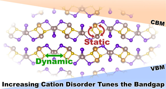
In conclusion, we determined the athermal ground-state structure of Sn2SbS2I3 to be the P21/c space group. We find significant cation disordering between 300 and 900 K and confirm the predicted disordered Cmcm room-temperature structure using X-ray diffraction. Disorder is found to drastically affect the electronic bandgap, while avoiding the detrimental presence of localized states. By controlling the crystal annealing temperature as well as the subsequent crystal cooling rate, the disorder and thus bandgap energies of this and potentially other A2BCh2X3 materials could be finely tuned, allowing the targeted application of these emerging earth-abundant absorber materials. The predicted disorder and defect tolerance would allow the design of a graded solar cell which avoids the formation of recombination sites at crystal boundaries due to variations in structure. Therefore, the minimally investigated group IV/V mixed-metal chalcohalide family (A = Pb, Sn, Ge; B = Sb, Bi; Ch = O, S, Se; X = I, Br, Cl) presents an exciting class of materials for optoelectronic applications.
Acknowledgments
We thank Stephan Lany and Jacob Cordell for sharing code to analyze IPR from DFT calculations. We thank Alex Ganose for a helpful discussion regarding transport properties. A.N. and S.R.K. acknowledge the EPSRC and SFI Centre for Doctoral Training in Advanced Characterisation of Materials (EP/S023259/1) for funding a Ph.D. studentship. The authors acknowledge the use of the UCL Kathleen and Thomas High Performance Computing Facility. Via membership of the UK’s HEC Materials Chemistry Consortium, which is funded by the EPSRC (EP/L000202, EP/R029431, EP/T022213), this work used the ARCHER2 UK National Supercomputing Service (www.archer2.ac.uk and the UK Materials and Molecular Modelling (MMM) Hub (Thomas – EP/P020194 and Young – EP/T022213). D.O.S. acknowledges support from the European Research Council, ERC (Grant No. 758345).
Data Availability Statement
All calculation data and analyses are provided in an online repository at 10.5281/zenodo.7276405.
Supporting Information Available
The Supporting Information is available free of charge at https://pubs.acs.org/doi/10.1021/jacs.2c13336.
Additional crystal structures, group–subgroup relationships, cluster expansion and Monte Carlo convergence plots, and further discussion of the electronic structure (PDF)
The authors declare no competing financial interest.
Supplementary Material
References
- Jeong J.; et al. Pseudo-Halide Anion Engineering for alpha-FAPbI3 Perovskite Solar Cells. Nature 2021, 592, 381–385. 10.1038/s41586-021-03406-5. [DOI] [PubMed] [Google Scholar]
- Laboratory, N.R.E. (2020). Best Research-Cell. Efficiencies. https://www.nrel.gov/pv/cell-efficiency.html, (accessed 2022–05–12).
- Huang Y.-T.; Kavanagh S. R.; Scanlon D. O.; Walsh A.; Hoye R. L. Z. Perovskite-Inspired Materials for Photovoltaics and beyond—from Design to Devices. Nanotechnology 2021, 32, 132004. 10.1088/1361-6528/abcf6d. [DOI] [PubMed] [Google Scholar]
- Ganose A. M.; Savory C. N.; Scanlon D. O. Beyond Methylammonium Lead Iodide: Prospects for the Emergent Field of ns2 Containing Solar Absorbers. Chem. Commun. 2017, 53, 20–44. 10.1039/C6CC06475B. [DOI] [PubMed] [Google Scholar]
- Nie R.; Sumukam R. R.; Reddy S. H.; Banavoth M.; Seok S. I. Lead-Free Perovskite Solar Cells Enabled by Hetero-Valent Substitutes. Energy Environ. Sci. 2020, 13, 2363–2385. 10.1039/D0EE01153C. [DOI] [Google Scholar]
- Chen W.; Dahliah D.; Rignanese G.-M.; Hautier G. Origin of the Low Conversion Efficiency in Cu2ZnSnS4 Kesterite Solar Cells: The Actual Role of Cation Disorder. Energy Environ. Sci. 2021, 14, 3567–3578. 10.1039/D1EE00260K. [DOI] [Google Scholar]
- Kavanagh S. R.; Walsh A.; Scanlon D. O. Rapid Recombination by Cadmium Vacancies in CdTe. ACS Energy Lett. 2021, 6, 1392–1398. 10.1021/acsenergylett.1c00380. [DOI] [PMC free article] [PubMed] [Google Scholar]
- Hadke S.; Huang M.; Chen C.; Tay Y. F.; Chen S.; Tang J.; Wong L. Emerging Chalcogenide Thin Films for Solar Energy Harvesting Devices. Chem. Rev. 2022, 122, 10170–10265. 10.1021/acs.chemrev.1c00301. [DOI] [PubMed] [Google Scholar]
- Savory C. N.; Ganose A. M.; Scanlon D. O. Exploring the PbS–Bi2S3 Series for Next Generation Energy Conversion Materials. Chem. Mater. 2017, 29, 5156–5167. 10.1021/acs.chemmater.7b00628. [DOI] [Google Scholar]
- Sopiha K. V.; Comparotto C.; Márquez J. A.; Scragg J. J. S. Chalcogenide Perovskites: Tantalizing Prospects, Challenging Materials. Advanced Optical Materials 2022, 10, 2101704. 10.1002/adom.202101704. [DOI] [Google Scholar]
- Nie R.; Lee K. S.; Hu M.; Paik M. J.; Seok S. I. Heteroleptic Tin-Antimony Sulfoiodide for Stable and Lead-free Solar Cells. Matter 2020, 3, 1701–1713. 10.1016/j.matt.2020.08.020. [DOI] [Google Scholar]
- Nie R.; Kim B.; Hong S.-T.; Seok S. I. Nanostructured Heterojunction Solar Cells Based on Pb2SbS2I3: Linking Lead Halide Perovskites and Metal Chalcogenides. ACS Energy Lett. 2018, 3, 2376–2382. 10.1021/acsenergylett.8b01332. [DOI] [Google Scholar]
- Pai N.; Lu J.; Gengenbach T. R.; Seeber A.; Chesman A. S. R.; Jiang L.; Senevirathna D. C.; Andrews P. C.; Bach U.; Cheng Y.-B.; Simonov A. N. Silver Bismuth Sulfoiodide Solar Cells: Tuning Optoelectronic Properties by Sulfide Modification for Enhanced Photovoltaic Performance. Adv. Energy Mater. 2019, 9, 1803396. 10.1002/aenm.201803396. [DOI] [Google Scholar]
- Nie R.; Seok S. I. Efficient Antimony-Based Solar Cells by Enhanced Charge Transfer. Small Methods 2020, 4, 1900698. 10.1002/smtd.201900698. [DOI] [Google Scholar]
- Olivier-Fourcade J.; Jumas J. C.; Maurin M.; Philippot E. Mise en Évidence d’un Nouveau Sulfoiodure d’Étain et d’Antimoine Sn2SbS2I3: Étude Structurale. Zeitschrift für anorganische und allgemeine Chemie 1980, 468, 91–98. 10.1002/zaac.19804680112. [DOI] [Google Scholar]
- Ibanez A.; Jumas J. C.; Olivier-Fourcade J.; Philippot E. Mise en évidence d’un désordre statistique dans les structures chalcogénoiodures d’étain et d’antimoine. J. Solid State Chem. 1984, 55, 83–91. 10.1016/0022-4596(84)90250-0. [DOI] [Google Scholar]
- Dolgikh V. New Chalkogen-Halogenides of the Type M2SbS2I3. Izv. Akad. Nauk SSSR, Neorg. Mater. 1985, 21, 1211–1214. [Google Scholar]
- Starosta V. I.; Kroutil J.; Beneš L. Preparation and Fundamental Physical Properties of Sn2SbS2I3 and Pb2SbS2I3 Compounds. Crystal Research and Technology 1990, 25, 1439–1442. 10.1002/crat.2170251214. [DOI] [Google Scholar]
- Islam S. M.; Malliakas C. D.; Sarma D.; Maloney D. C.; Stoumpos C. C.; Kontsevoi O. Y.; Freeman A. J.; Kanatzidis M. G. Direct Gap Semiconductors Pb2BiS2I3, Sn2BiS2I3, and Sn2BiSI5. Chem. Mater. 2016, 28, 7332–7343. 10.1021/acs.chemmater.6b02691. [DOI] [Google Scholar]
- Palazon F. Metal Chalcohalides: Next Generation Photovoltaic Materials?. Solar RRL 2022, 6, 2100829. 10.1002/solr.202100829. [DOI] [Google Scholar]
- Yang C.; Wang Z.; He G.; Zhang H.; Liao C. Pb2BiS2I3 Nanowires for Use in Photodetectors. ACS Appl. Nano Mater. 2022, 5, 1603316038. 10.1021/acsanm.2c03958. [DOI] [Google Scholar]
- Kavanagh S. R.; Savory C. N.; Scanlon D. O.; Walsh A. Hidden Spontaneous Polarisation in the Chalcohalide Photovoltaic Absorber Sn2SbS2I3. Mater. Horiz. 2021, 8, 2709–2716. 10.1039/D1MH00764E. [DOI] [PMC free article] [PubMed] [Google Scholar]
- Butler K. T.; Frost J. M.; Walsh A. Ferroelectric Materials for Solar Energy Conversion: Photoferroics Revisited. Energy Environ. Sci. 2015, 8, 838–848. 10.1039/C4EE03523B. [DOI] [Google Scholar]
- Doussier C.; Moëlo Y.; Léone P.; Meerschaut A.; Evain M. Crystal Structure of Pb2SbS2I3, and Re-Examination of the Crystal Chemistry within the Group of (Pb/Sn/Sb) Chalcogeno-Iodides. Solid State Sci. 2007, 9, 792–803. 10.1016/j.solidstatesciences.2007.07.003. [DOI] [Google Scholar]
- Chantler C. T. Theoretical Form Factor, Attenuation, and Scattering Tabulation for Z = 1–92 from E = 1–10 eV to E = 0.4–1.0 MeV. J. Phys. Chem. Ref. Data 1995, 24, 71–643. 10.1063/1.555974. [DOI] [Google Scholar]
- Momma K.; Izumi F. VESTA: A Three-Dimensional Visualization System for Electronic and Structural Analysis. J. Appl. Crystallogr. 2008, 41, 653–658. 10.1107/S0021889808012016. [DOI] [Google Scholar]
- Kresse G.; Hafner J. Ab Initio Molecular Dynamics for Liquid Metals. Phys. Rev. B 1993, 47, 558–561. 10.1103/PhysRevB.47.558. [DOI] [PubMed] [Google Scholar]
- Kresse G.; Hafner J. Ab Initio Molecular-Dynamics Simulation of the Liquid-Metal-Amorphous-Semiconductor Transition in Germanium. Phys. Rev. B 1994, 49, 14251–14269. 10.1103/PhysRevB.49.14251. [DOI] [PubMed] [Google Scholar]
- Kresse G.; Furthmüller J. Efficiency of Ab-Initio Total Energy Calculations for Metals and Semiconductors Using a Plane-Wave Basis Set. Comput. Mater. Sci. 1996, 6, 15–50. 10.1016/0927-0256(96)00008-0. [DOI] [PubMed] [Google Scholar]
- Kresse G.; Furthmüller J. Efficient Iterative Schemes for Ab Initio Total-Energy Calculations Using a Plane-Wave Basis Set. Phys. Rev. B 1996, 54, 11169–11186. 10.1103/PhysRevB.54.11169. [DOI] [PubMed] [Google Scholar]
- Kresse G.; Joubert D. From Ultrasoft Pseudopotentials to the Projector Augmented-Wave Method. Phys. Rev. B 1999, 59, 1758–1775. 10.1103/PhysRevB.59.1758. [DOI] [Google Scholar]
- Klimeš J.; Bowler D. R.; Michaelides A. Van Der Waals Density Functionals Applied to Solids. Phys. Rev. B 2011, 83, 195131. 10.1103/PhysRevB.83.195131. [DOI] [Google Scholar]
- Lozano A.; Escribano B.; Akhmatskaya E.; Carrasco J. Assessment of van Der Waals Inclusive Density Functional Theory Methods for Layered Electroactive Materials. Phys. Chem. Chem. Phys. 2017, 19, 10133–10139. 10.1039/C7CP00284J. [DOI] [PubMed] [Google Scholar]
- Ångqvist M.; Muñoz W. A.; Rahm J. M.; Fransson E.; Durniak C.; Rozyczko P.; Rod T. H.; Erhart P. ICET – A Python Library for Constructing and Sampling Alloy Cluster Expansions. Advanced Theory and Simulations 2019, 2, 1900015. 10.1002/adts.201900015. [DOI] [Google Scholar]
- Hart G. L. W.; Forcade R. W. Algorithm for Generating Derivative Structures. Phys. Rev. B 2008, 77, 224115. 10.1103/PhysRevB.77.224115. [DOI] [Google Scholar]
- Hart G. L. W.; Forcade R. W. Generating Derivative Structures from Multilattices: Algorithm and Application to Hcp Alloys. Phys. Rev. B 2009, 80, 014120. 10.1103/PhysRevB.80.014120. [DOI] [Google Scholar]
- O’Rourke C.; Morgan B. J. Crystal-Torture: ACrystal Tortuosity Module. Journal of Open Source Software 2019, 4, 1306. 10.21105/joss.01306. [DOI] [Google Scholar]
- van de Walle A.; Tiwary P.; de Jong M.; Olmsted D. L.; Asta M.; Dick A.; Shin D.; Wang Y.; Chen L. Q.; Liu Z. K. Efficient Stochastic Generation of Special Quasirandom Structures. Calphad 2013, 42, 13–18. 10.1016/j.calphad.2013.06.006. [DOI] [Google Scholar]
- Ong S. P.; Richards W. D.; Jain A.; Hautier G.; Kocher M.; Cholia S.; Gunter D.; Chevrier V. L.; Persson K. A.; Ceder G. Python Materials Genomics (Pymatgen): A Robust, Open-Source Python Library for Materials Analysis. Comput. Mater. Sci. 2013, 68, 314–319. 10.1016/j.commatsci.2012.10.028. [DOI] [Google Scholar]
- Heyd J.; Scuseria G. E.; Ernzerhof M. Hybrid Functionals Based on a Screened Coulomb Potential. J. Chem. Phys. 2003, 118, 8207–8215. 10.1063/1.1564060. [DOI] [Google Scholar]
- Krukau A. V.; Vydrov O. A.; Izmaylov A. F.; Scuseria G. E. Influence of the Exchange Screening Parameter on the Performance of Screened Hybrid Functionals. J. Chem. Phys. 2006, 125, 224106. 10.1063/1.2404663. [DOI] [PubMed] [Google Scholar]
- Ibañez-Azpiroz J.; Tsirkin S. S.; Souza I. Ab Initio Calculation of the Shift Photocurrent by Wannier Interpolation. Phys. Rev. B 2018, 97, 245143. 10.1103/PhysRevB.97.245143. [DOI] [Google Scholar]
- Pizzi G.; et al. Wannier90 as a Community Code: New Features and Applications. J. Phys.: Condens. Matter 2020, 32, 165902. 10.1088/1361-648X/ab51ff. [DOI] [PubMed] [Google Scholar]
- Ganose A. M.; Jackson A. J.; Scanlon D. O. Sumo: Command-line Tools for Plotting and Analysis of Periodic Ab Initio Calculations. Journal of Open Source Software 2018, 3, 717. 10.21105/joss.00717. [DOI] [Google Scholar]
- Zhu B.; Kavanagh S. R.. Easyunfold. https://github.com/SMTG-UCL/easyunfold (accessed 2023–02–10).
- Sheldrick G. M. A Short History of SHELX. Acta Cryst. A 2008, 64, 112–122. 10.1107/S0108767307043930. [DOI] [PubMed] [Google Scholar]
- Sheldrick G. M. Crystal Structure Refinement with SHELXL. Acta Cryst. C 2015, 71, 3–8. 10.1107/S2053229614024218. [DOI] [PMC free article] [PubMed] [Google Scholar]
- Brese N. E.; O’Keeffe M. Bond-Valence Parameters for Solids. Acta Cryst. B 1991, 47, 192–197. 10.1107/S0108768190011041. [DOI] [Google Scholar]
- O’Keefe M.; Brese N. E. Atom Sizes and Bond Lengths in Molecules and Crystals. J. Am. Chem. Soc. 1991, 113, 3226–3229. 10.1021/ja00009a002. [DOI] [Google Scholar]
- Wang Y.; Kavanagh S. R.; Burgués-Ceballos I.; Walsh A.; Scanlon D. O.; Konstantatos G. Cation Disorder Engineering Yields AgBiS2 Nanocrystals with Enhanced Optical Absorption for Efficient Ultrathin Solar Cells. Nat. Photonics 2022, 16, 235–241. 10.1038/s41566-021-00950-4. [DOI] [Google Scholar]
- Yang J.; Zhang P.; Wei S.-H. Band Structure Engineering of Cs2AgBiBr6 Perovskite through Order–Disordered Transition: A First-Principle Study. J. Phys. Chem. Lett. 2018, 9, 31–35. 10.1021/acs.jpclett.7b02992. [DOI] [PubMed] [Google Scholar]
- Scanlon D. O.; Walsh A. Bandgap Engineering of ZnSnP2 for High-Efficiency Solar Cells. Appl. Phys. Lett. 2012, 100, 251911. 10.1063/1.4730375. [DOI] [Google Scholar]
- Monserrat B.; Park J.-S.; Kim S.; Walsh A. Role of Electron-Phonon Coupling and Thermal Expansion on Band Gaps, Carrier Mobility, and Interfacial Offsets in Kesterite Thin-Film Solar Cells. Appl. Phys. Lett. 2018, 112, 193903. 10.1063/1.5028186. [DOI] [Google Scholar]
- Huang Y.-T.; et al. Strong Absorption and Ultrafast Localisation in NaBiS2 Nanocrystals with Slow Charge-Carrier Recombination. Nat. Commun. 2022, 13, 4960. 10.1038/s41467-022-32669-3. [DOI] [PMC free article] [PubMed] [Google Scholar]
- Veal T. D.; Feldberg N.; Quackenbush N. F.; Linhart W. M.; Scanlon D. O.; Piper L. F. J.; Durbin S. M. Band Gap Dependence on Cation Disorder in ZnSnN2 Solar Absorber. Adv. Energy Mater. 2015, 5, 1501462. 10.1002/aenm.201501462. [DOI] [Google Scholar]
- Lany S.; Fioretti A. N.; Zawadzki P. P.; Schelhas L. T.; Toberer E. S.; Zakutayev A.; Tamboli A. C. Monte Carlo Simulations of Disorder in ZnSnN2 and the Effects on the Electronic Structure. Phys. Rev. Materials 2017, 1, 035401. 10.1103/PhysRevMaterials.1.035401. [DOI] [Google Scholar]
- Cordell J. J.; Tucker G. J.; Tamboli A.; Lany S. Bandgap Analysis and Carrier Localization in Cation-Disordered ZnGeN2. APL Materials 2022, 10, 011112. 10.1063/5.0077632. [DOI] [Google Scholar]
- Kang Y.; Cho Y.; Han S. Cation Disorder as the Major Electron Scattering Source in Crystalline InGaZnO. Appl. Phys. Lett. 2013, 102, 152104. 10.1063/1.4802093. [DOI] [Google Scholar]
- Brandt R. E.; Poindexter J. R.; Gorai P.; Kurchin R. C.; Hoye R. L. Z.; Nienhaus L.; Wilson M. W. B.; Polizzotti J. A.; Sereika R.; Žaltauskas R.; Lee L. C.; MacManus-Driscoll J. L.; Bawendi M.; Stevanović V.; Buonassisi T. Searching for “Defect-Tolerant” Photovoltaic Materials: Combined Theoretical and Experimental Screening. Chem. Mater. 2017, 29, 4667–4674. 10.1021/acs.chemmater.6b05496. [DOI] [Google Scholar]
- Walsh A.; Zunger A. Instilling defect tolerance in new compounds. Nat. Mater. 2017, 16, 964–967. 10.1038/nmat4973. [DOI] [PubMed] [Google Scholar]
- Kim S.; Park J.-S.; Hood S.; Walsh A. Lone-Pair Effect on Carrier Capture in Cu 2 ZnSnS 4 Solar Cells. Journal of Materials Chemistry A 2019, 7, 2686–2693. 10.1039/C8TA10130B. [DOI] [Google Scholar]
- Jin X.; Fang Y.; Salim T.; Feng M.; Hadke S.; Leow S. W.; Sum T. C.; Wong L. H. In Situ Growth of [hk1]-Oriented Sb2S3 for Solution-Processed Planar Heterojunction Solar Cell with 6.4% Efficiency. Adv. Funct. Mater. 2020, 30, 2002887. 10.1002/adfm.202002887. [DOI] [Google Scholar]
- Zhou Y.; Wang L.; Chen S.; Qin S.; Liu X.; Chen J.; Xue D.-J.; Luo M.; Cao Y.; Cheng Y.; Sargent E. H.; Tang J. Thin-Film Sb2Se3 Photovoltaics with Oriented One-Dimensional Ribbons and Benign Grain Boundaries. Nat. Photonics 2015, 9, 409–415. 10.1038/nphoton.2015.78. [DOI] [Google Scholar]
Associated Data
This section collects any data citations, data availability statements, or supplementary materials included in this article.
Supplementary Materials
Data Availability Statement
All calculation data and analyses are provided in an online repository at 10.5281/zenodo.7276405.