Abstract
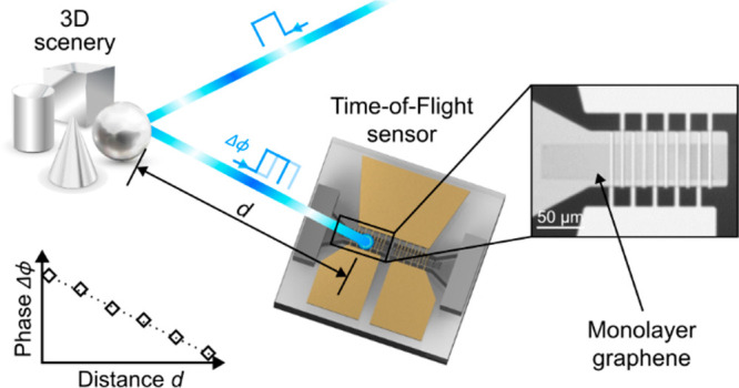
A large and growing number of applications benefit from innovative and powerful 3D image sensors. Graphene photodetectors can achieve 3D sensing functionalities by intrinsic optoelectronic frequency mixing due to the nonlinear output characteristics of the sensor. In first proof of principle distance measurement demonstrations, we achieve modulation frequencies of 3.1 MHz, signal-to-noise ratios of ∼40 dB, distance detection up to at least 1 m, and a mean accuracy of 25.6 mm. The scalable More than Moore detector approach enables geometrical fill factors close to 100% and can easily complement powerful functionalities by simple back-end integration on top of CMOS electronics.
Keywords: graphene, time-of-flight (ToF), range sensor, distance measurement, superheterodyning, 3d imaging, optoelectronics, optoelectronic mixer, 3d sensor
3D vision is a fundamental cornerstone for highly complex tasks in the future fields of autonomous driving for scene recognition1,2 or novel manufacturing and quality tests for Industry 4.0.3−5 The medical sector,6 human recognition7 and scanning,8 and scene analysis in security applications for crowd screening9 can benefit from high-performance 3D camera systems as well as the entertainment sector,10,11 which pioneered widespread 3D imaging systems and awareness with the first generation of Microsoft’s Kinect.12 Because most applications differ in their requirements, research and industry developed various depth measurement and 3D imaging concepts, each with its own advantages and challenges. However, the objective of all systems is to improve overall performance characteristics, especially lateral precision and resolution, speed of image acquisition for real-time applications, reliability, and integrability, e.g., for mobile or space-limited systems.
State-of-the-art 3D imaging systems typically use either triangulation13,14 or the time-of-flight (ToF)15 principle. Systems based on triangulation utilize geometries and special configurations to compute depth information from optical data. These systems are subdivided into (I) passive systems, such as stereo vision8 or dynamic vision13 entailing significant drawbacks and limitations in demanding applications, and (II) active systems that compensate for many of these limitations. The structured light approach, for example, uses specific light patterns to illuminate the scene, using diffraction of the reflected pattern to compute depth information, achieving depth resolutions of at least a several tenths of a micometer.16 However, triangulation-based systems inevitably require multiple active elements, preventing highly integrated devices or miniaturized systems. This approach is also error-prone, as it has difficulty detecting uniformly shaped or monochromatic objects.
ToF methods such as the light detection and ranging (LiDAR)17 or photonic mixer devices (PMD)18 exploit the finite speed of light and utilize the difference between light emission and detection of photons reflected from the scene. The propagation time results in the distance. ToF principles range from (I) direct methods to accurately measure propagation time requiring very precise timing and fast sensors, (II) indirect methods that modulate the emitted light and measure the phase delay due to the propagation time, and (III) frequency modulated methods2 that allow depth resolutions in the range of a few millimeters for less complex devices19 down to several tenths of a micrometer for very complex and time-consuming techniques.20 These approaches allow for very large-scale integration, e.g., enabling 3D in mobile applications, and do not suffer from scene-dependent uncertainties such as objects. However, today’s approaches rely on highly complex sensor architectures or systems, such as scanning systems involving sensitive micromirrors, linked with extensive readout complexity and signal processing (e.g., mixing and circuitry).
The claim of this paper is the use of graphene21 for indirect ToF paving the way to overcome bandwidth limitations of silicon-based technology and simplifying the sensor architecture by exploiting nonlinearities resulting in internal optoelectronic frequency mixing. Graphene can exhibit charge carrier mobilities above 200 000 cm2 V–1 s–1,22 allowing bandwidths far beyond that of state-of-the-art silicon devices. Furthermore, the linear dispersion relation of graphene allows for an unlimited choice of illumination wavelengths and thus does not restrict applications due to light or laser safety limitations.23
Although mixing of two optical24 or two electrical signals25 has already been demonstrated in graphene as well as optoelectronic mixing at modulation frequencies above 65 GHz26,27 in highly optimized device structures, previous articles only mention 3D imaging to be a potential application lacking further demonstration.
In this work, we demonstrate for the first time a metal–graphene–metal photonic mixer device (MGM-PMD) for optical distance measurements exploiting internal optoelectronic frequency mixing. Proof of concept measurements show that operation frequencies in the megahertz range can easily be achieved without relying on complex device architectures or e-beam lithography.
Conventional PMDs require a highly precise gate control and complex readout circuitry (I) to separate charge carriers between two integrated readout diodes and (II) to detect a phase shift of the incoming amplitude-modulated light. An electrical circuit-based cross-correlation of both the modulated gate and the optical signal reflected from the scene results in 3D sensing capabilities. In contrast, the PMD functionality demonstrated in this work is provided by the MGM-PMD itself because an intrinsic frequency mixing of the electrical gate modulation with the optical modulation27 occurs due to nonlinearities in graphene. Besides reduced integration efforts (no differential readout of two diodes is necessary), the complexity of an electrical circuitry for signal generation and to detect and evaluate accumulated charge on the respective readout diodes is significantly reduced. In the following section, the device technology and fabrication steps are presented.
Figure 1 shows the process chain of the MGM-PMD fabrication. At first, trenches for the buried gate contacts have been wet chemically etched into the glass substrate (Figure 1a) followed by chromium (Cr) gate contact deposition (Figure 1b) and aluminum oxide (Al2O3) passivation (Figure 1c). In a next step, interdigitated metal finger structures consisting of chromium/gold (Cr/Au) have been deposited (Figure 1d) prior to the monolayer graphene transfer (Figure 1e). Finally, a further Al2O3 passivation layer has been deposited on top of the MGM-PMD (Figure 1f) in order to protect the device from environmental influences, which, for example, cause unwanted doping.28 Further details on the MGM-PMD fabrication are given in the Methods section. A false-color Raman mapping image of the metal–graphene–metal photodetector on a glass substrate (purple) with graphene channel (cyan), source and drain Cr/Au contacts (yellow), and the buried gate Cr contact (black) without passivation layer is shown in the close-up (black rectangle) in Figure 1.
Figure 1.
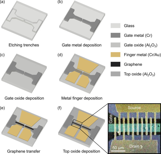
(a–f) Schematic representation of the technological fabrication steps for the MGM-PMD. The close-up (black rectangle) shows the Raman mapping image in false colors of a metal–graphene–metal photodetector on a glass substrate (purple) with graphene channel (cyan), source and drain Cr/Au contacts (yellow), and the buried gate Cr contact (black). Raman analyses were performed without Al2O3 passivation to obtain a low noise image.
2D material qualities (crystallinity and defect density) have been monitored by Raman spectroscopic analysis (cf. Figure 2a). The small D-peak indicates a low defect density in monolayer graphene stating the good initial graphene quality and thorough PMMA-assisted graphene transfer.
Figure 2.
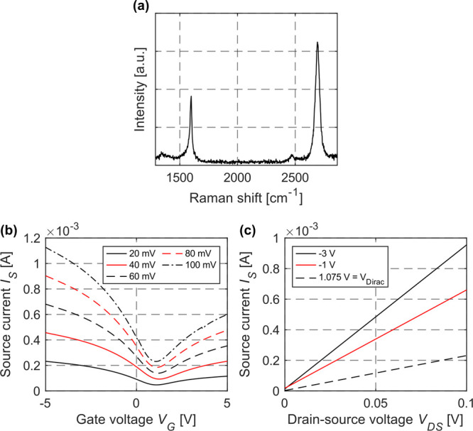
(a) Raman spectrum of the graphene channel. The peaks characteristic for p-doped graphene29,30 (G-peak at 1598 cm–1 and 2D-peak at 2693 cm–1) are clearly visible. The low intensity of the D-peak at 1348 cm–1 indicates a high quality of the graphene with few defects. The excitation wavelength of the laser is 532 nm. (b) IS–VG curves for drain–source biases of VDS = 20 to 100 mV (ΔVDS = 20 mV) and (c) IS–VDS curves for gate biases of VG = −3 to 1.075 V.
Prior to the distance measurements, current–voltage (I–V) measurements were performed to electrically characterize the devices. First, the source current (IS) has been determined to be a function of the gate voltage (VG) (Figure 2b) showing the expected nonlinear behavior. From the results presented in Figure 2b, charge carrier mobilities have been extracted with the direct transconductance method (DTM) as proposed by Zhong et al.31 considering the GFET as a parallel connection of transistors. Taking this consideration into account, the effective channel width Weff is given by the channel width WCh multiplied by the number of gaps between the fingers (details on the finger structure are given below). Utilizing the DTM, electron and hole mobilities of μe = 140 cm2 V–1 s–1 and μh = 266 cm2 V–1 s–1 have been extracted for VDS = 100 mV, respectively. Compared to conventional semiconductor or other graphene-based devices, the mobilities presented in this work are comparatively low because CVD graphene has been used in conjunction with additional encapsulation of graphene in between Al2O3 and SiO2 that reduce mobilities further. Furthermore, source current vs drain–source voltage (VDS) curves have been acquired, showing resistance behavior (Figure 2c). For the first-ever distance measurement demonstration, the gate has been modulated because the behavior of IS as a function of VG is highly nonlinear (Figure 2b), whereas IS linearly depends on VDS (Figure 2c). Previously, it has been shown that VDS modulation can also be used to generate optoelectronic mixing in a graphene device, but at considerably higher channel bias voltages of at least 3 V and optical power exceeding 20 mW.32
In order to estimate device and design specific modulation frequencies prior to experimental 3D measurements, the gate–drain, gate–source, and drain–source capacitance of the structure have been determined in a material- and architecture-specific manner. In this context, the drain–source capacity CDS for MSM finger structures can be estimated within 2% accuracy for the sensor geometry presented here taking into account the following relationship:33,34
| 1 |
where N is the finger pair number, WCh is the width of the graphene channel, εr is the permittivity number, WF is the finger width, and L is the finger spacing. This interpolation considers the layer thickness of the contact material tCon to be much smaller than the finger width W (tCon ≪ W). The drain–source capacitance of the MGM-PMD prototype is CDS = 7.2 fF (N = 5, WCh = 29.02 μm, εr,Graphene = 6.9,35W = 4.17 μm, L = 11.22 μm, t = 135 nm). According to Mao et al.,36 the gate–source/gate–drain capacitance is to a first approximation CGS/GD = ∼12 pF (εr,Al2O3 = 9.5, tAl2O3 = 20 nm). In this first ever demonstration, the modulation frequency of the graphene PMD achievable in the current design is significantly dominated by the gate capacitance. Considering the experimentally determined maximum sensor resistance of R = 427 Ω at the Dirac point, the 3 dB cutoff frequency is found to be fg ≈ 31 MHz. According to this estimation, electrical and optical modulation frequencies have been chosen far below the 3 dB cutoff frequency in first distance measurement demonstrations utilizing graphene-based mixing devices to ensure sufficiently high signal-to-noise ratios of the sensor output signal as demonstrated in the next section (cf. Figure 4).
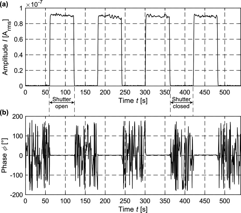
Figure 4.
(a) Transient behavior of the mixed signal amplitude at fmix = 6 Hz for an electrical modulation of fel = 3 130 860 Hz and an optical modulation of fopt = 3130866 Hz; (b) the corresponding phase with the shutter open (= stable phase) and closed (gate voltage VG = 3 Vpp with an DC offset VDC = −2 V, drain–source bias of VDS = 10 mV, I–U gain 104, laser wavelength λlaser = 405 nm and irradiance Ee = 328 mW/mm2 (respectively, laser power Plaser = 10 mW)).
A schematic of the optical distance measurement setup utilizing 2D material-based MGM photodetectors is presented in Figure 3. The setup includes a 405 nm amplitude modulated laser, a motorized linear stage with a retroreflector, an electromechanical shutter, a function generator, a current–voltage amplifier, a lock-in amplifier, and a voltage source. The device under test (DUT) is contacted electrically using probe needles. The drain contact is biased utilizing a DC voltage supply to ensure charge transport across the channel region by spanning up an electrical field. The optical modulation signal fopt from the function generator serves as an input for the laser source. The same signal is fed into a lock-in amplifier, which internally generates a difference frequency of fopt and a freely adjustable frequency fel that is provided by the lock-in amplifier itself. The signal fel serves as the electrical modulation signal for the gate of the MGM-PMD. This measurement technique ensures that the lock-in amplifier reliably detects the differential frequency |fopt – fel| being generated by the DUT. In a next stage, the optoelectronically mixed current signal of the DUT is amplified (gain 104) and converted to a voltage which is then used as input signal for the lock-in amplifier. The motorized linear stage is used to move the retroreflector and utilized to change the distance from the sample to the light source. The laser beam can be blocked by means of an electromechanical shutter. A high-speed photoreceiver with a crystalline Si-PIN photodiode (iC212, iC-Haus GmbH) connected to a conventional oscilloscope is used to monitor the optically modulated signal.
Figure 3.
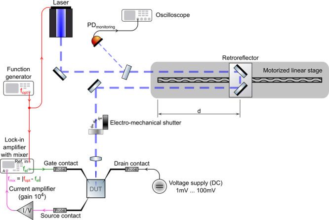
Schematic representation of the measurement setup for ToF distance measurements using a graphene-based MGM-PMD. In this configuration, the lock-in amplifier has been set to lock onto the difference frequency internally generated from the electrical modulation signal (fel) and the optical modulation frequency (fopt).
Figure 4 shows the time-resolved signal amplitude (top) as well as the corresponding phase ϕ (bottom) of the mixed signal (fmix = 6 Hz) for an optical modulation of fopt = 3 130 866 Hz and an electrical modulation of fel = 3 130 860 Hz. In this experiment, modulation frequencies have been chosen to generate a mixed frequency component below 50 Hz to block parasitic environmental noise, especially mains hum. Both graphs depict a stable mixing signal with the shutter open for a fixed distance d = 0 mm (cf. Figure 3). The distance measurement has been conducted using a gate modulation voltage of VG = 3 Vpp (DC offset VDC = −2 V) and a drain–source bias of VDS = 10 mV. From the incident laser power (Plaser = 10 mW) and a detected mixing current of 0.09 μA, a sensitivity of ∼0.1 mA W–1 for the mixed signal can be derived at that operating point. The signal located at the differential frequency fmix exhibits an excellent phase stability of 0.56° corresponding to a depth resolution of ∼75 mm at 3.13 MHz with the shutter open. In time-of-flight optical distance measurements, a high phase stability of the sensor is a prerequisite to achieve a high depth resolution. The signal-to-noise ratio of the differential frequency components amplitude signal of the MGM-PMD exceeds values of 40 dB, indicating that in further experiments light intensities might be reduced or distances increased. In a next step, the nonlinear output characteristic of the graphene sensor has been exploited to demonstrate time-of-flight optical distance measurements.
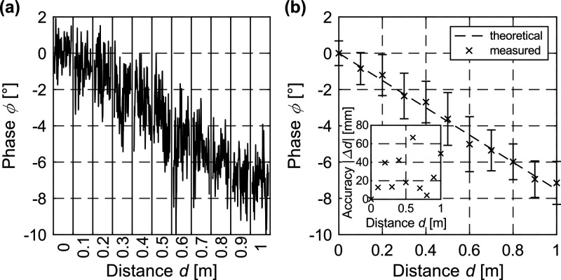
The distance measurement functionality of the MGM-PMD is verified experimentally in Figure 5, where Figure 5a represents the raw data and Figure 5b the mean values extracted from it. Here, the theoretical (expected) and the measured phase shift of the MGM sensor output are shown as a function of the distance d. As expected, the phase of the mixed signal is almost proportional to the distance, here shown for distances up to at least 1 m. The theoretical phase as a function of depth for ToF imagers has been calculated according to37
| 2 |
where c is the speed of light, ϕ is the phase, and fm is the modulation frequency. The mean accuracy,2 i.e., the deviation from the theoretical phase, is found to be 25.6 mm. The experimental results presented here clearly verify and demonstrate that the nonlinear behavior of 2D material graphene enables optical distance measurements by optoelectronic frequency mixing. The simple sensor design approach can achieve fill factors close to 100% whereas conventional time-of-flight detector concepts stagnate at 22%.38,39 A huge benefit is the simple back-end integration on top of semiconductor electronics or flexible substrates, enabling additional sensor functionalities and performance on-chip, making the MGM-PMD a More than Moore device.40 The detector presented here is thus a promising candidate to compete with alternative high-performance More than Moore devices in the future. The equipment used for distance measurement, such as function generator, lock-in amplifier, current amplifier, or stand-alone laser, can later be replaced by integrated devices. For example, if the differential frequency is fixed (defined by the two modulation frequencies fel and fopt), the lock-in amplifier can be implemented by integrating either simple narrow bandwidth filters or more sophisticated phase sensitive detector (PSD) and low-pass filter below the sensor as part of the readout electronics.
Figure 5.
First experimental demonstration of a distance measurement using our MGM-PMD for distances up to 1 m. Distance-dependent phase shift of the mixed signal (fmix = 6 Hz) for fel = 3130860 Hz and fopt = 3130866 Hz. The results were obtained at a gate voltage VG = 3 Vpp (VDC = −2 V), a drain–source bias of VDS = 10 mV, a wavelength of 405 nm, an irradiance of Ee = 328 mW/mm2, and a laser power of Plaser = 10 mW. (a) Raw data of the phase for different distances. (b) Mean values including error bars for the raw data shown in (a). Inset: accuracy extracted from the experiment, with a mean accuracy of 25.6 mm.
In conclusion, intrinsic optoelectronic frequency mixing in graphene-based MGM-PMDs has been systematically investigated and utilized for optical distance measurements. The mixing effect thereby is enabled by the nonlinear output and transfer characteristics of the detector. The MGM-PMDs enable range measurements, hence 3D measurement capabilities, at modulation frequencies up to at least 3.1 MHz and mixing frequencies of 6 Hz in first proof of principle demonstrations. A distance of up to at least 1 m and an accuracy of ∼26 mm have been successfully demonstrated. A signal-to-noise ratio of ∼40 dB indicates that the current detection limit of 10 mW, corresponding to an irradiance of 328 mW/mm2, might be reduced in further experiments. Utilizing the innovative 2D material technology approach, sensor architectures and material compositions can further be developed towards fast, highly accurate, and sensitive distance measurement detectors and systems. The very simple device architecture and fabrication is scalable and allows for sensor integration on top of silicon electronics with fill factors close to 100%. This approach can enable significant performance improvements of 3D imaging systems compared to existing technologies.
Methods
MGM-PMDs have been fabricated onto conventional glass substrates (D 263 T eco, SCHOTT). Prior to the contact deposition and graphene transfer, the substrates have been thoroughly cleaned. Subsequent patterning utilizes standard UV lithography (MJB3, SUSS MicroTec). In a first step, 100 nm deep trenches have been etched chemically by a buffered hydrofluoric acid (BOE 7-1 (AF 87.5-12.5) avec Surfactant) solution to define the buried gate contact areas. Next, 100 nm chromium has been deposited by RF sputtering at 13.56 MHz to fill the trenches followed by atomic layer deposition (ALD) to create a gate oxide layer of Al2O3 with a thickness of 20 nm. This gate oxide has been patterned and etched back in the gate contact area with BOE in order to contact the gates electrically. After that, source and drain areas have been defined in another lithography step. RF sputtering followed by a lift-off process has been applied to realize interdigitated Cr/Au (15 nm/120 nm) finger contacts. Single-layer graphene has been grown on top of a copper foil in a Moorfield NanoCVD-8G system by thermal assisted chemical vapor deposition. The graphene monolayers have been transferred by a conventional wet method using spin-coated poly(methyl methacrylate) (PMMA) as a support for the graphene. The 2D film has been separated from the growth substrate by etching the copper in sodium persulfate (Na2S2O8). The PMMA-supported graphene has been transferred onto deionized water for cleaning and fished out with the prepatterned target substrate. The PMMA has been thoroughly removed by a multistep process using ultraclean solvents. In a next step, graphene channels have been patterned and etched by reactive ion etching with an oxygen plasma. Finally, a passivation layer of SiO2/Al2O3 (5 nm/80 nm) has been deposited on top of the MGM-PMD graphene channel serving as a protective layer against ambient influences (the evaporated SiO2 is required as a barrier layer to avoid damaging the graphene during the ALD process).
Raman studies have been performed using a confocal microscope (TE 300, Nikon) and a laser (COMPASS 315M-100, Coherent) with a wavelength of 532 nm and a maximum excitation power of 100 mW. The signal has been collected through a 40× objective (NA 0.6, Nikon) and was detected using a monochromator (Triax 320, Horiba Jobin Yvon GmbH) and an EMCCD camera (Newton DU970P-BV, Andor Oxford Instruments).
Electrical device characterization comprises I–V measurements that have been performed using a SUSS microprobe station, connected to a Keithley 4200-SCS parameter analyzer.
Phase sensitive signals have been converted using a FEMTO DLPCA-200 I–V converter and amplifier and acquired via lock-in technique (SR865A, Stanford Research Systems). Distance measurements have been performed using an Omicrometer LDM405D.180.150 laser diode module with a peak wavelength of 405 nm. The power on the detector has been determined by a crystalline silicon reference detector (OP-2 VIS, Coherent) and a laser power meter (FieldMaxII-TO, Coherent).
Acknowledgments
The authors gratefully thank the European Regional Development Funds in North Rhine-Westphalia (EFRE.NRW) for funding this research project (EFRE0200545). Prof. Dr. Max C. Lemme and Martin Otto from AMO GmbH as well as Dr. Gerrit Lükens from RWTH Aachen are given credit for the atomic layer deposition of Al2O3 acting as gate oxide and passivation layer for the devices.
The authors declare no competing financial interest.
References
- Rasshofer R. H.; Gresser K. Automotive Radar and Lidar Systems for Next Generation Driver Assistance Functions. Adv. Radio Sci. 2005, 3, 205–209. 10.5194/ars-3-205-2005. [DOI] [Google Scholar]
- Roriz R.; Cabral J.; Gomes T. Automotive LiDAR Technology: A Survey. IEEE Transactions on Intelligent Transportation Systems 2022, 23 (7), 6282–6297. 10.1109/TITS.2021.3086804. [DOI] [Google Scholar]
- Zhang S.Handbook of 3D Machine Vision: Optical Metrology and Imaging; CRC Press: 2013; p 414. [Google Scholar]
- Hochdorfer S.; Schlegel C. 6 DoF SLAM Using a ToF Camera: The Challenge of a Continuously Growing Number of Landmarks. 2010 IEEE/RSJ. International Conference on Intelligent Robots and Systems 2010, 3981–3986. 10.1109/IROS.2010.5651229. [DOI] [Google Scholar]
- Pinto A. M.; Costa P.; Moreira A. P.; Rocha L. F.; Veiga G.; Moreira E. Evaluation of Depth Sensors for Robotic Applications. 2015 IEEE International Conference on Autonomous Robot Systems and Competitions 2015, 139–143. 10.1109/ICARSC.2015.24. [DOI] [Google Scholar]
- Rengier F.; Mehndiratta A.; von Tengg-Kobligk H.; Zechmann C. M.; Unterhinninghofen R.; Kauczor H.-U.; Giesel F. L. 3D Printing Based on Imaging Data: Review of Medical Applications. Int. J. CARS 2010, 5 (4), 335–341. 10.1007/s11548-010-0476-x. [DOI] [PubMed] [Google Scholar]
- Premebida C.; Carreira J.; Batista J.; Nunes U. Pedestrian Detection Combining RGB and Dense LIDAR Data. 2014 IEEE/RSJ. International Conference on Intelligent Robots and Systems 2014, 4112–4117. 10.1109/IROS.2014.6943141. [DOI] [Google Scholar]
- Bartol K.; Bojanić D.; Petković T.; Pribanić T. A Review of Body Measurement Using 3D Scanning. IEEE Access 2021, 9, 67281–67301. 10.1109/ACCESS.2021.3076595. [DOI] [Google Scholar]
- Patel K.; Han H.; Jain A. K. Secure Face Unlock: Spoof Detection on Smartphones. IEEE Transactions on Information Forensics and Security 2016, 11 (10), 2268–2283. 10.1109/TIFS.2016.2578288. [DOI] [Google Scholar]
- Tam W. J.; Speranza F.; Yano S.; Shimono K.; Ono H. Stereoscopic 3D-TV: Visual Comfort. IEEE Transactions on Broadcasting 2011, 57 (2), 335–346. 10.1109/TBC.2011.2125070. [DOI] [Google Scholar]
- Kolb A.; Barth E.; Koch R.; Larsen R. Time-of-Flight Cameras in Computer Graphics. Computer Graphics Forum 2010, 29 (1), 141–159. 10.1111/j.1467-8659.2009.01583.x. [DOI] [Google Scholar]
- Han J.; Shao L.; Xu D.; Shotton J. Enhanced Computer Vision With Microsoft Kinect Sensor: A Review. IEEE Transactions on Cybernetics 2013, 43 (5), 1318–1334. 10.1109/TCYB.2013.2265378. [DOI] [PubMed] [Google Scholar]
- Soatto S.; Frezza R.; Perona P. Motion Estimation via Dynamic Vision. IEEE Transactions on Automatic Control 1996, 41 (3), 393–413. 10.1109/9.486640. [DOI] [Google Scholar]
- Uchida N.; Shibahara T.; Aoki T.; Nakajima H.; Kobayashi K. 3D Face Recognition Using Passive Stereo Vision. IEEE International Conference on Image Processing 2005 2005, 2, II–950. 10.1109/ICIP.2005.1530214. [DOI] [Google Scholar]
- Foix S.; Alenya G.; Torras C. Lock-in Time-of-Flight (ToF) Cameras: A Survey. IEEE Sensors Journal 2011, 11 (9), 1917–1926. 10.1109/JSEN.2010.2101060. [DOI] [Google Scholar]
- Traxler L.; Ginner L.; Breuss S.; Blaschitz B. Experimental Comparison of Optical Inline 3D Measurement and Inspection Systems. IEEE Access 2021, 9, 53952–53963. 10.1109/ACCESS.2021.3070381. [DOI] [Google Scholar]
- Behroozpour B.; Sandborn P. A. M.; Wu M. C.; Boser B. E. Lidar System Architectures and Circuits. IEEE Communications Magazine 2017, 55 (10), 135–142. 10.1109/MCOM.2017.1700030. [DOI] [Google Scholar]
- Schwarte R.; Xu Z.; Heinol H.-G.; Olk J.; Klein R.; Buxbaum B.; Fischer H.; Schulte J.. New Electro-Optical Mixing and Correlating Sensor: Facilities and Applications of the Photonic Mixer Device (PMD). In Sensors, Sensor Systems, and Sensor Data Processing; International Society for Optics and Photonics: 1997; Vol. 3100, pp 245–253. [Google Scholar]
- Lee S.; Park D.; Lee S.; Choi J.; Kim S.-J. Design of a Time-of-Flight Sensor With Standard Pinned-Photodiode Devices Toward 100-MHz Modulation Frequency. IEEE Access 2019, 7, 130451–130459. 10.1109/ACCESS.2019.2940259. [DOI] [Google Scholar]
- Murray R.; Lyons A. Two-Photon Interference LiDAR Imaging. Opt. Express 2022, 30 (15), 27164. 10.1364/OE.461248. [DOI] [PubMed] [Google Scholar]
- Novoselov K. S.; Geim A. K.; Morozov S. V.; Jiang D.; Zhang Y.; Dubonos S. V.; Grigorieva I. V.; Firsov A. A. Electric Field Effect in Atomically Thin Carbon Films. Science 2004, 306 (5696), 666–669. 10.1126/science.1102896. [DOI] [PubMed] [Google Scholar]
- Bolotin K. I.; Sikes K. J.; Jiang Z.; Klima M.; Fudenberg G.; Hone J.; Kim P.; Stormer H. L. Ultrahigh Electron Mobility in Suspended Graphene. Solid State Commun. 2008, 146 (9–10), 351–355. 10.1016/j.ssc.2008.02.024. [DOI] [Google Scholar]
- Novoselov K. S.; Fal′ko V. I.; Colombo L.; Gellert P. R.; Schwab M. G.; Kim K. A Roadmap for Graphene. Nature 2012, 490 (7419), 192–200. 10.1038/nature11458. [DOI] [PubMed] [Google Scholar]
- Cheng C.; Huang B.; Mao X.; Zhang Z.; Zhang Z.; Geng Z.; Xue P.; Chen H. Frequency Conversion with Nonlinear Graphene Photodetectors. Nanoscale 2017, 9 (12), 4082–4089. 10.1039/C6NR08964J. [DOI] [PubMed] [Google Scholar]
- Tong J.; Conte M. C.; Goldstein T.; Yngvesson S. K.; Bardin J. C.; Yan J. Asymmetric Two-Terminal Graphene Detector for Broadband Radiofrequency Heterodyne- and Self-Mixing. Nano Lett. 2018, 18 (6), 3516–3522. 10.1021/acs.nanolett.8b00574. [DOI] [PubMed] [Google Scholar]
- Hamidouche L.; Montanaro A.; Rosticher M.; Grimaldi E.; Poupet B.; Taniguchi T.; Watanabe K.; Plaçais B.; Baudin E.; Legagneux P. Optoelectronic Mixing in High-Mobility Graphene. ACS Photonics 2021, 8 (1), 369–375. 10.1021/acsphotonics.0c01679. [DOI] [Google Scholar]
- Montanaro A.; Wei W.; De Fazio D.; Sassi U.; Soavi G.; Aversa P.; Ferrari A. C.; Happy H.; Legagneux P.; Pallecchi E. Optoelectronic Mixing with High-Frequency Graphene Transistors. Nat. Commun. 2021, 12 (1), 2728. 10.1038/s41467-021-22943-1. [DOI] [PMC free article] [PubMed] [Google Scholar]
- Kienitz P.; Bablich A.; Bornemann R.; Bolívar P. H.. Photonic Mixer Device (PMD) Based on Graphene for High-Resolution 3D Sensors. In 2D Photonic Materials and Devices IV; International Society for Optics and Photonics: 2021; Vol. 11688, p 116880S. [Google Scholar]
- Das A.; Pisana S.; Chakraborty B.; Piscanec S.; Saha S. K.; Waghmare U. V.; Novoselov K. S.; Krishnamurthy H. R.; Geim A. K.; Ferrari A. C.; Sood A. K. Monitoring Dopants by Raman Scattering in an Electrochemically Top-Gated Graphene Transistor. Nat. Nanotechnol. 2008, 3 (4), 210–215. 10.1038/nnano.2008.67. [DOI] [PubMed] [Google Scholar]
- Kalbac M.; Reina-Cecco A.; Farhat H.; Kong J.; Kavan L.; Dresselhaus M. S. The Influence of Strong Electron and Hole Doping on the Raman Intensity of Chemical Vapor-Deposition Graphene. ACS Nano 2010, 4 (10), 6055–6063. 10.1021/nn1010914. [DOI] [PubMed] [Google Scholar]
- Zhong H.; Zhang Z.; Xu H.; Qiu C.; Peng L.-M. Comparison of Mobility Extraction Methods Based on Field-Effect Measurements for Graphene. AIP Adv. 2015, 5 (5), 057136. 10.1063/1.4921400. [DOI] [Google Scholar]
- Montanaro A.; Mzali S.; Mazellier J.-P.; Bezencenet O.; Larat C.; Molin S.; Morvan L.; Legagneux P.; Dolfi D.; Dlubak B.; Seneor P.; Martin M.-B.; Hofmann S.; Robertson J.; Centeno A.; Zurutuza A. Thirty Gigahertz Optoelectronic Mixing in Chemical Vapor Deposited Graphene. Nano Lett. 2016, 16 (5), 2988–2993. 10.1021/acs.nanolett.5b05141. [DOI] [PubMed] [Google Scholar]
- Averine S. V.; Chan Y. C.; Lam Y. L. Geometry Optimization of Interdigitated Schottky-Barrier Metal–Semiconductor–Metal Photodiode Structures. Solid-State Electron. 2001, 45 (3), 441–446. 10.1016/S0038-1101(01)00017-X. [DOI] [Google Scholar]
- Farnell G. W.; Cermak I. A.; Silverster P.; Wong S. K. Capacitance and Field Distributions for Interdigital Surface-Wave Transducers. IEEE Transactions on Sonics and Ultrasonics 1970, 17 (3), 188–195. 10.1109/T-SU.1970.29560. [DOI] [Google Scholar]
- Fang J.; Vandenberghe W. G.; Fischetti M. V. Microscopic Dielectric Permittivities of Graphene Nanoribbons and Graphene. Phys. Rev. B 2016, 94 (4), 045318. 10.1103/PhysRevB.94.045318. [DOI] [Google Scholar]
- Mao Q.; Wen Q.-Y.; Tian W.; Wen T.-L.; Chen Z.; Yang Q.-H.; Zhang H.-W. High-Speed and Broadband Terahertz Wave Modulators Based on Large-Area Graphene Field-Effect Transistors. Opt. Lett., OL 2014, 39 (19), 5649–5652. 10.1364/OL.39.005649. [DOI] [PubMed] [Google Scholar]
- Ringbeck T.; Möller T.; Hagebeuker B. Multidimensional Measurement by Using 3-D PMD Sensors. Advances in Radio Science 2007, 5, 135–146. 10.5194/ars-5-135-2007. [DOI] [Google Scholar]
- Hussmann S.; Ringbeck T.; Hagebeuker B.. A Performance Review of 3D TOF Vision Systems in Comparison to Stereo Vision Systems; IntechOpen: 2008. [Google Scholar]
- Lange R.; Böhmer S.; Buxbaum B.. 11 - CMOS-Based Optical Time-of-Flight 3D Imaging and Ranging. In High Performance Silicon Imaging, 2nd ed.; Durini D., Ed.; Woodhead Publishing Series in Electronic and Optical Materials; Woodhead Publishing: 2020; pp 319–375. [Google Scholar]
- Zhang G. Q.; van Roosmalen A.. More than Moore: Creating High Value Micro/Nanoelectronics Systems; Springer Science & Business Media: 2009; p 338. [Google Scholar]


