Abstract
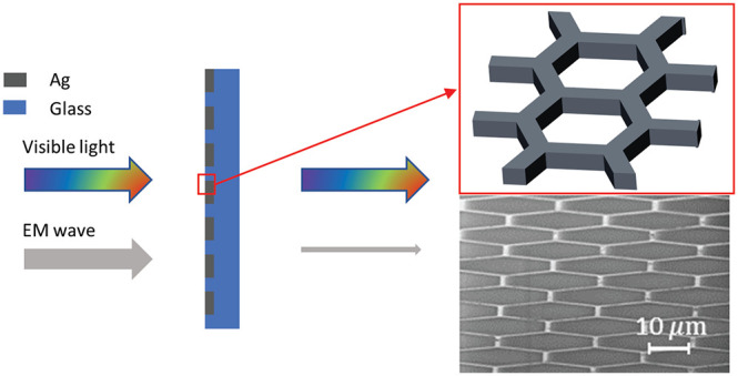
We present a simulation and experimental study of silver meshes to determine their performance for transparent electromagnetic interference (EMI) shielding. Simulations were employed to study the effects of the silver mesh’s width, pitch, and thickness on EMI shielding efficiency (SE) in the 8–18 GHz frequency range and transparency in the visible spectrum. We demonstrate a scalable, facile fabrication method that involves embedding meshes in glass by etching trenches in glass and filling and curing reactive particle-free silver ink in these trenches. Our silver meshes achieve 58.4 dB EMI SE with 83% visible light transmission and 48.3 dB EMI SE with 90.3% visible transmission. The combination of high-conductivity silver, small widths (1.3 to 5 μm), and large thicknesses (0.5 to 2.0 μm) enables the best performance of metal meshes as well as single-sided shielding materials for transparent EMI shielding, as reported in the literature.
Keywords: EMI shielding, Metal ink, Reactive ion etching, Photolithography, Metal mesh, Transparent electrode
Introduction
The increasing complexity and widespread use of electronic devices and systems has led to growing demand for new types of electromagnetic interference (EMI) shielding materials and fabrication methods.1 EMI shielding materials are needed to reduce the impact of surrounding radiation on electronic components and to prevent their functionality or accuracy from being compromised or their lifetimes from being shortened.2,3 In addition to protecting electronic components, EMI shielding can provide security from sensitive information being compromised2,4 or from electronic systems being disabled by electromagnetic pulse weapons or attacks.5,6 EM radiation may also have negative effects on human health.4
In many optoelectronic devices, such as heated windows, smart displays, and wearable electronics, it is required that the shielding material achieves both high shielding efficiency (SE) and high visible light transmission (T). Transparent EMI shielding has, thus, been the focus of much research. One category of transparent EMI shielding consists of thin film structures. High conductivity metals such as silver (Ag), copper (Cu), and nickel (Ni) are used to form a conductive film to reflect and absorb EM waves. Materials with a high refraction index such as indium tin oxide (ITO) or zinc oxide (ZnO) may be used to surround the metal film in order to increase transparency by leveraging destructive interference to reduce reflected light.7 It has been reported that ITO/Ag–Cu/ITO film structures have achieved 26 dB SE and 96.5% visible transmission.8 ZnO/Ag/ZnO sandwich structures have been reported with 35 dB SE and 88.9% transmission in the visible range.9 The theoretical performance limits of these thin film structures were explored in our previous paper.7 We determined that titania/Ag/titania (TiO2/Ag/TiO2) film structures could achieve 41.2 dB SE with 90.8% visible transmission. These simulations suggest that it is unlikely for these sandwich structures to achieve higher than 45 dB SE while maintaining over 90% visible transmission.
Another category of transparent EMI shielding consists of metal meshes.10,11 Since visible light is comprised of EM radiation with smaller wavelengths than microwaves, this approach uses metal meshes with an intermediate pitch to enable visible light to pass through the open areas, while blocking the larger wavelength microwaves. Ni meshes on ITO have achieved 92% optical transmission with 40 dB SE.12 The meshes were fabricated by patterning photoresist through laser direct-writing followed by nickel electrodeposition to create meshes with widths of 5 μm and thicknesses ranging from 2.5 to 6.0 μm.12 This approach was developed further to achieve double-layer nickel meshes on PET to achieve an average SE of 42.5 dB and a transmission of 88.7%.13 The width of the Ni mesh is 6.5 μm and thickness is 4 μm. Multi-ring Al meshes have exhibited 90% transmission with 27 dB SE.14 These multi-ring meshes were fabricated by photolithography followed by dry etching of the aluminum and achieved line widths of about 2.5 μm and thickness of 0.2 μm. Cu meshes with an average SE of 41 dB and transmission of 85% have been fabricated by thermal evaporation of Cr/Cu onto a crack lithography pattern, which created meshes with a width of 5 μm and thickness of up to about 1 μm.15 Liang et al. have demonstrated Cu meshes have been fabricated by ion beam etching Cr/Cu films after photoresist patterning to achieve 45 dB SE and 85% transmission.16 These Cr/Cu meshes have a width of 0.85 μm and thickness of 0.5 μm. These Cr/Cu meshes represent the highest performing transparent EMI shielding for meshes with visible transparency greater than or equal to 80% transmission with a SE of 45 dB. The best performing EMI shielding for meshes with visible transparency greater than or equal to 90% are the Ni meshes by Jiang et al. with widths of 5 μm and thicknesses ranging from 2.5 to 6.0 μm that have demonstrated an SE of 40 dB.12
The EMI SE performance of metal nanomeshes, such as those of Ni, Al, and Cu, may, in principle, be improved with Ag, which has the highest conductivity of all metals. However, results with Ag meshes have been inferior to those of other metals. Ag metal meshes have been reported to achieve 90.5% optical transmission with 26 dB SE.17 These Ag metal meshes were fabricated by electric-field-driven microscale 3D printing and have a line width of 26 μm. Ag meshes patterned by photolithography and metal lift-off have exhibited a transmittance of 92% and SE of 28.8 dB.18 These meshes have a width of 6 μm and a thickness of 0.2 μm. Ag/Cu and Ag/Ni meshes have also been fabricated by sputtering Ag onto a crack lithography template followed by galvanic deposition of Cu or Ni.19 An average SE of 38.5 dB with transmission of 85.4% was achieved with a width of 5.5 μm and a thickness of about 0.25 μm. While Ag has the potential for achieving a higher performance in transparent EMI shielding compared to other metals due to its high conductivity,20 this improved performance has yet to be realized.
In this paper, we present both a simulation and an experimental study of metal meshes for transparent EMI shielding. We performed simulations to provide for understanding of the relationships between width, pitch, and thickness of metal meshes and their influence on EMI SE and visible transparency. Our simulations indicate that a small width and large thickness are key to achieving high performance. These simulations suggest that the large widths and small thicknesses of Ag meshes fabricated thus far are the reasons for their suboptimal performance.
We demonstrate the facile, scalable fabrication of Ag meshes with an unprecedented combination of small widths and large thicknesses to achieve record performance. Previous transparent EMI shielding work with metal meshes has not been demonstrated with reactive ink-based fabrication approaches. Glass-embedded metal meshes were fabricated by etching trenches into glass using lithography and reactive ion etching (RIE). Reactive, high conductivity Ag ink was used to fill the trenches via a low temperature curing process (under 110 °C). We demonstrate Ag meshes that exhibit an EMI SE of 58.4 dB with 83% visible transmission and Ag meshes with an EMI SE of 48.3 dB and 90.3% visible transmission. This is the record highest transparent EMI shielding performance for metal meshes and the highest performance for single-sided structures of any kind. The metal meshes have a width of 1.6 μm and thickness of 0.8 μm and a width of 3.5 μm and thickness of 1.0 μm, respectively. Metal meshes embedded in glass substrates with thicknesses up to 2.0 μm, which are planarized with the glass surface, are demonstrated and may be utilized for a variety of optoelectronic applications. These metal meshes achieve the best transparent EMI shielding performance due to the combination of the use of high-conductivity silver, small widths, and large thicknesses.
Results and Discussion
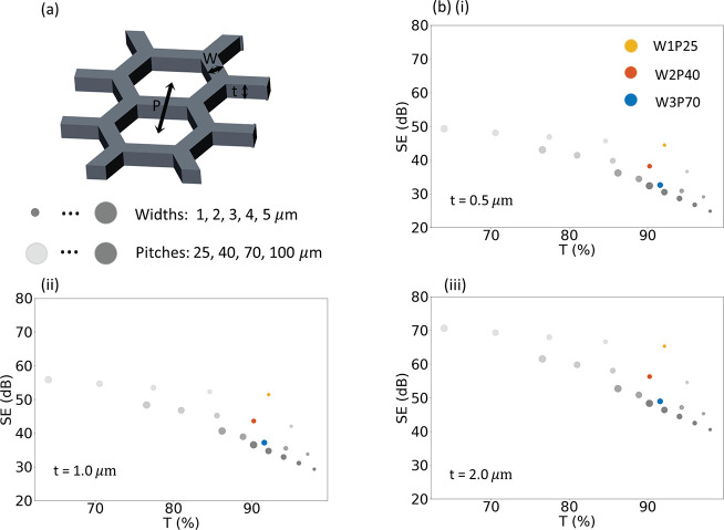
Figure 1 shows (a) a schematic of the metal mesh and (b) the simulation results for metal meshes. The metal meshes are defined by their width W, pitch P, and thickness t. High-frequency electromagnetic field simulation using the finite element method was used to predict EMI SE performance.21−23 The details of the simulations are provided in Table S1. Since the pitches studied are much larger than that of visible light, the 550 nm transmission was calculated from the geometric ratio of open area to total area:
| 1 |
The simulation results are shown in Figure 1b for three different thicknesses: t = (i) 0.5, (ii) 1.0, and (iii) 2.0 μm. The conductivity of the silver is assumed to be 1.3 × 10⁷ S/m or 20% that of bulk silver. The size of the circle in the plots is proportional to the width of the meshes, where the widths of 1, 2, 3, 4, and 5 μm were simulated. The darkness of the circle indicates the pitch of the meshes, and four different pitches of 25, 40, 70, and 100 μm were simulated.
Figure 1.
High-frequency electromagnetic field simulation results of average EMI shielding efficiency at 8–18 GHz for Ag meshes with different pitches, widths, and thicknesses. (a) Schematic of hexagonal Ag mesh defined by width W, pitch P, and thickness t. (b) Simulation results for metal meshes with widths of 1, 2, 3, 4, 5 μm, pitches of 25, 40, 70, 100 μm, and for three thicknesses of (i) 0.5, (ii) 1, and (iii) 2 μm.
The trade-offs between EMI SE and optical transparency can be observed in the simulation results. Increasing the width for the same thickness and pitch results in higher EMI SE due to increased metal coverage at the expense of visible transparency. Conversely, as the pitch increases while keeping the same thickness and width reduces EMI SE, while improving visible transparency. The two metrics of EMI SE and optical transparency can be evaluated through the concept of Pareto optimality, where it is impossible to improve one metric without making the other aspect worse. In this context, the simulation results indicate that smaller width meshes provide better results compared to meshes with larger width. For the same transparency, a higher EMI SE may be achieved with smaller width meshes. Furthermore, for the same width and pitch mesh, it is desirable to fabricate thicker meshes, which can improve the SE for a given T. As the pitch of meshes is easily adjustable, the key to obtaining high-performance EMI SE is fabricating meshes of small width and large thickness. Increasing thickness is crucial for enhancing performance because a 1 μm increase in thickness has a greater impact on transparent EMI SE than a 1 μm decrease in width.
The smallest width Ag meshes that have been fabricated thus far are Ag/Cu meshes with 5.5 μm width.19 These meshes have a thickness of only 0.25 μm. This large width and small thickness limit the performance of these meshes to an EMI SE of 38.5 dB and visible transmission of 85.4%. There is a need to fabricate silver meshes with smaller widths and larger thicknesses to enable better performance. Toward this goal, we demonstrate a large-area, low-cost method to fabricate Ag meshes with small width and large thickness. Three meshes of varying nominal widths W of 1, 2, and 3 μm and pitches of 25, 40, and 70 μm, respectively, were studied in more detail through experiments. The three meshes are labeled W1P25, W2P40, and W3P70, which indicate their width and pitch in microns. For example, W1P25 refers to a mesh width of 1 μm and pitch of 25 μm. These three meshes are shown in Figure 1 with yellow, red, and blue circles, respectively.
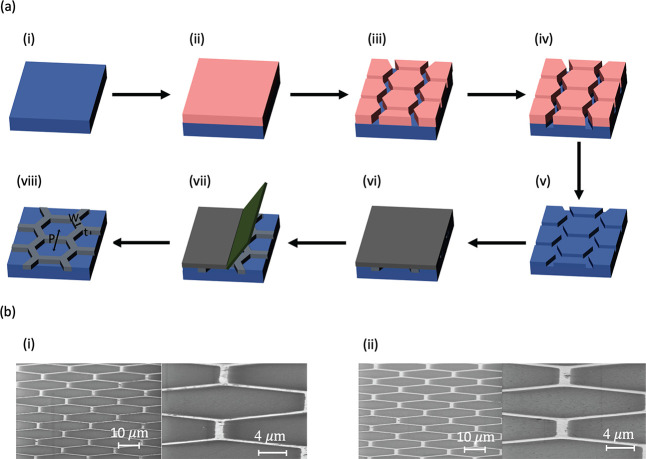
Figure 2a shows a schematic of the fabrication process. A glass substrate (Figure 2a,i) is coated with photoresist (Figure 2a,ii), and a hexagonal pattern is transferred to this photoresist using maskless photolithography (Figure 2a,iii). The hexagonal pattern is transferred into the glass substrate by RIE (Figure 2a,iv). Then the photoresist is stripped (Figure 2a,v). Ag ink is coated onto the glass by spin coating and then cured (Figure 2a,vi). The Ag is scratched off using a blade (Figure 2a,vii) revealing the hexagonal structure (Figure 2a,viii). The coating, curing, and scratching steps are repeated again to ensure complete trench filling.
Figure 2.
(a) Schematic of glass-embedded Ag meshes fabrication process: (i) transparent glass substrate, (ii) photoresist coating, (iii) photolithography, (iv) reactive-ion etching, (v) photoresist removal, (vi) Ag ink coating and curing, (vii) removal of Ag by a razor blade, and finally (viii) glass-embedded Ag mesh. The Ag meshes are hexagonal arrays embedded into a glass substrate, defined by width W, pitch P, and thickness t. (b) Scanning electron microscopy (SEM) images of (i) W1P25t0.5 and (ii) W1P25t0.8 samples taken at an 80° angle from directly overhead with actual widths of 1.3 and 1.6 μm, respectively.
Six different metal mesh samples were fabricated of varying widths, pitches, and thicknesses. For each of three different mesh pitch and width combinations (W1P25, W2P40, and W3P70), two different thickness meshes were fabricated. Figure S1 shows the trench profile of the six different samples as characterized by optical profilometry prior to the Ag ink coating. A consistent vertical etch rate of ∼1.2 nm/s is observed in the samples. However, while the etching is primarily vertical, there is also some lateral etching, resulting in the etched trenches have a trapezoidal cross-section as opposed to a rectangular one. The Ag ink coating and scratching are performed twice to ensure complete trench filling. Figure S2 shows optical profilometry analysis of one of the metal mesh samples (W3P70t1.0) prior to the Ag ink coating, after one coat, and then after a second coat. The cured Ag only partially fills the trenches due to the large reduction in volume from solvent evaporation during the Ag ink curing process. The final cured silver is planar with the unetched glass, which may be beneficial for applications such as organic light emitting diodes (OLEDs) and solar cells. The fabricated samples are uniform with no traces of silver residue in between the meshes. Atomic force microscopy (AFM) characterization of the final metal mesh reveals very small roughness. Figure S3 illustrates the characterization of the surface roughness of the same metal mesh sample by AFM. The root-mean-square roughness (Rq) of the silver is 6.7 nm.
The width and thickness of the samples that were fabricated were measured by scanning electron microscopy (SEM) and the samples are summarized in Table 1. Figure 2b shows SEM images of the W1P25t0.5 and W1P25t0.8 samples. These samples were etched for 400 and 700 s, respectively. The W1P25t0.5 sample has a measured width of 1.3 μm and a thickness of 0.5 μm, while the W1P25t0.8 sample exhibits a measured width of 1.6 μm and a thickness of 0.8 μm.
Table 1. Summary of the Etch Time, Measured Thickness, and Measured Width for Various Samples Fabricated.
| Number | Sample | .Etch Time (s) | t (μm) | Wm (μm) |
|---|---|---|---|---|
| 1 | W1P25 | 400 | 0.5 | 1.3 |
| 2 | W1P25 | 700 | 0.8 | 1.6 |
| 3 | W2P40 | 800 | 1.0 | 2.8 |
| 4 | W2P40 | 1300 | 1.6 | 3.2 |
| 5 | W3P70 | 800 | 1.0 | 3.5 |
| 6 | W3P70 | 1600 | 2.0 | 5.0 |
Based on the simulation results discussed, it is desirable to fabricate metal meshes with a width W as narrow as possible and a thickness t as large as possible. The pitch can be set arbitrarily. However, the meshes width and pitch are not independent parameters. In order to achieve small width meshes, thinner photoresist must be used. The thicknesses of the photoresist for the W1, W2, and W3 samples are 0.6, 2, and 2.8 μm, respectively. This limits the thickness achievable in the metal meshes as the thickness of the photoresist limits how long the glass can be etched. There are thus trade-offs between the narrowness of width achievable and the depth of the trench achievable. This trade-off between width and thickness translates to trade-offs in transmission and SE that are achievable.
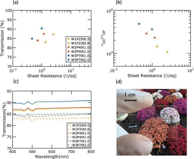
The optical performance of the six different Ag mesh samples was characterized. Figure 3 shows the optical transmission results. Figure 3a shows the transmission at a 550 nm wavelength and the sheet resistance of the six samples. For a particular mesh width and pitch combination, the shorter etch time results in a smaller measured width and a smaller thickness (indicated with a triangle), while the longer etch time results in a larger measured width and a larger thickness (indicated with a square). Etching the samples longer thus results in a smaller transmission with a smaller sheet resistance. The transmission for all the samples is in the range of 83.0–90.3% with the sheet resistance Rs in the range of 0.46–2.47 Ω per sq. The direct transmission of all six samples was characterized and the hazes for all the samples are shown in Table S2. The optical transmission is primarily due to direct transmission as the haze values are all 7.0% or lower.
Figure 3.
Optical performance of glass-embedded Ag meshes for three different combinations of pitch and width and different etch times: (a) transmission versus sheet resistance, (b) figure of merit σDC/σOP, (c) transmission versus wavelength, and (d) optical image of W1P25t0.5 with T = 87.2% at 550 nm.
Figure 3b plots the figure of merit (σDC/σOP) for various metal meshes as a function of Rs. The figure of merit is used for comparing transparent electrodes and is determined by the ratio between the dc conductivity (σDC) and the optical conductivity (σOP). A higher figure of merit indicates a more efficient device, which is able to transmit a larger amount of electrical current while still maintaining good optical transparency. The figure of merit is related to T and Rs by
| 2 |
where Z0 = 377 Ω is the free space impedance. Mesh samples achieve σDC/σOP in the range of 1000–4900, which are comparable to the best transparent electrodes in the literature.24−28Figure 3c shows the variation of transmission versus wavelength in the visible range. The transparency spectrum across the visible wavelength range is fairly flat. Figure 3d shows the optical image of the 30 mm × 30 mm W1P25t0.5 sample, which exhibits T = 87.2% at a wavelength of 550 nm. The uniformity and clarity of the sample can be seen in the image.
Figure 4 shows the EMI SE for the six different metal mesh samples. EMI shielding performance was characterized by the coaxial transmission line method.29 The shielding effectiveness is given by
| 3 |
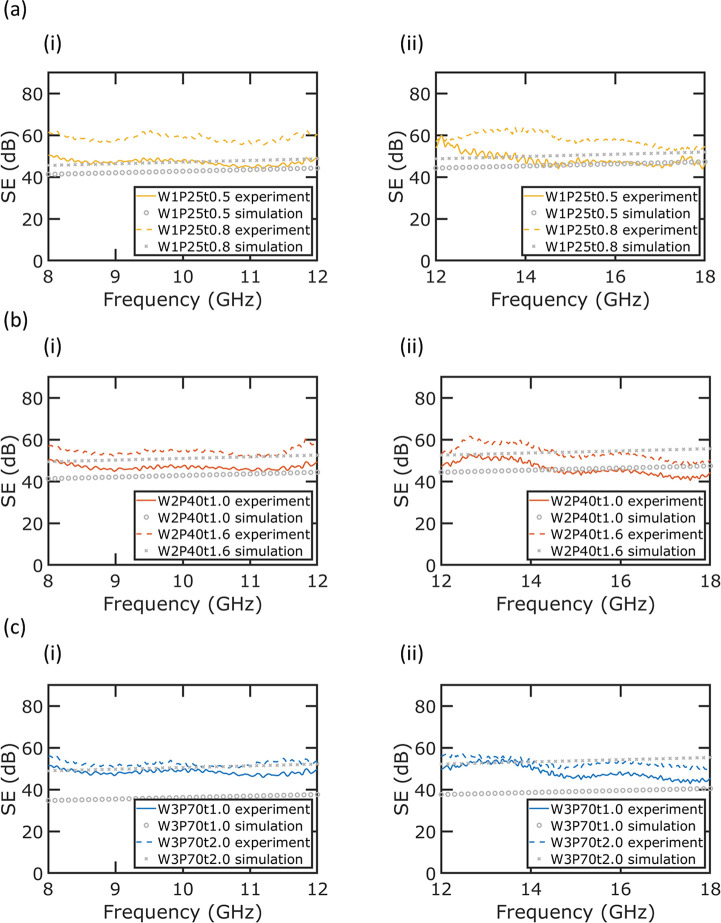
where Tm is the transmission coefficient of the sample at the microwave frequency of interest. Figures 4a shows the EMI SE performance of the (i) W1P25t0.5 and (ii) W1P25t0.8 samples. The shorter etched sample (W1P25t0.5) has an average EMI SE of 47.1 dB at frequencies ranging from 8–12 GHz and 48.6 dB from 12–18 GHz, while the longer etched sample (W1P25t0.8) has an average EMI SE of 58.6 dB between 8–12 GHz and 58.2 dB between 12–18 GHz. Figure 4b shows the EMI SE performance of the (i) W2P40t1.0 and (ii) W2P40t1.6 samples. The shorter etched sample (W2P40t1.0) has an average EMI SE of 46.8 dB between 8–12 GHz and 45.9 dB from 12–18 GHz and the longer etched sample (W2P40t1.6) has an average EMI SE of 54.4 dB between 8–12 GHz and 53.8 dB from 12–18 GHz. The SE of the fabricated samples in this paper has a low dependency on frequency range from 8–18 GHz, which makes them suitable for a variety of applications. Figure 4c shows the EMI SE performance of (i) W3P70t1.0 and (ii) W3P70t2.0 samples. The shorter etched sample (W3P70t1.0) has an average EMI SE of 48.4 dB from 8–12 GHz and 48.3 dB from 12–18 GHz, while the longer etched sample (W3P70t2.0) has an average EMI SE of 52.5 dB from 8–12 GHz and 53.0 dB from 12–18 GHz. Simulation results for these different metal meshes are also included.
Figure 4.
EMI shielding efficiency experimental and simulation results of (a) W1P25t0.5 and W1P25t0.8 samples, (b) W2P40t1.0 and W2P40t1.6 samples, and (c) W3P70t1.0 and W3P70t2.0 samples at (i) 8–12 GHz and (ii) 12–18 GHz.
For a particular pitch and width combination, the longer etch treatment leads to a lower optical transmission and higher EMI SE. This is because the longer etch time results in a larger width due to lateral etching. Shorter etched metal meshes could be used for applications such as shielding windows and display devices,30 which require higher optical transmission, while longer etched meshes could be used for medical devices and military applications,31 which require higher EMI SE.
Table 2 provides a comparison of the simulation and experimental measurement for T, SE, and Rs of all the fabricated samples in this paper. The simulated T simply comes from eq 1, and thus only depends on the width and pitch. Simulated SE and Rs consider the measured thickness and width, which are calculated from SEM images. A silver conductivity of 1.3 × 10⁷ S/m or 20% that of bulk silver is used as described above. Good agreement can be seen between the simulation and experimental results. The experimentally measured SE tends to be higher than that of simulations. This may be because the cured Ag meshes are porous, which may result in multiple reflections and an increase in EMI SE performance due to increased absorption.
Table 2. Comparison of the Simulation and Experimental Results for Our Six Fabricated Metal Meshesa.
| Simulations |
Experiments |
||||||
|---|---|---|---|---|---|---|---|
| Number | Sample | T (%) | SE (dB) | Rs (Ω/sq) | T (%) | SE (dB) | Rs (Ω/sq) |
| 1 | W1P25t0.5 | 89.9 | 44.8 | 1.84 | 87.2 | 48.0 | 2.47 |
| 2 | W1P25t0.8 | 87.6 | 49.3 | 0.95 | 83.0 | 58.4 | 1.33 |
| 3 | W2P40t1.0 | 86.5 | 44.9 | 0.58 | 87.4 | 46.3 | 1.16 |
| 4 | W2P40t1.6 | 84.6 | 53.1 | 0.35 | 83.9 | 54.0 | 0.71 |
| 5 | W3P70t1.0 | 90.3 | 38.1 | 0.75 | 90.3 | 48.3 | 0.99 |
| 6 | W3P70t2.0 | 86.2 | 52.7 | 0.29 | 84.9 | 52.8 | 0.46 |
The transparency (T) at 550 nm, average shielding efficiency (SE) from 8 to 18 GHz, and sheet resistance (Rs) are all presented.
Silver meshes exhibit a combination of reflection and absorption shielding mechanisms. Figure 5 shows the shielding contribution in the six samples from these two components: SE = SER + SEA, where SER represents the shielding efficiency between 8 and 18 GHz due to reflection, and SEA corresponds to the shielding efficiency between 8 and 18 GHz resulting from absorption. These two components are defined by
| 4 |
where R denotes the reflection coefficient and
| 5 |
The SER values for the six samples are all about the same at 13.1, 13.1, 13.0, 13.1, 13.2, and 13.1 dB, respectively. In contrast, the SEA values for the six samples are 34.9, 45.3, 33.3, 40.9, 35.1, and 39.7 dB, respectively. Absorption is the primary mechanism of EMI shielding effectiveness for the Ag metal mesh.
Figure 5.
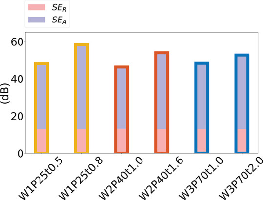
SE contribution of SEA and SER for six samples.
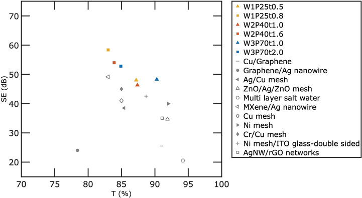
In Figure 6, we compared EMI SE (dB) and transmission of our six fabricated metal–metal meshes with transparent EMI shielding in the literature. This includes Cu/Graphene,32 Graphene/Ag nanowire,33 Ni mesh/ITO glass,13 Ag/Cu mesh,19 ZnO/Ag/ZnO,9 multilayer salt water,34 ITO/Ag–Cu/ITO,8 MXene/Ag nanowire,35 Cu mesh,15 Ni mesh,12 Cr/Cu mesh,16 Ni mesh-double-sided,13 and AgNW/rGO networks.36 It should be noted that different papers investigate various frequency ranges and report SE values as maximum, minimum, or average. However, to ensure consistency with the current paper, the average SE in the range of 8–18 GHz is reported here. The details of the comparison results of this paper with other works in the literature can be found in Table S3 of the Supporting Information.
Figure 6.
Comparison of the EMI SE (dB) and transmission (at 550 nm) of our six microgrids with other metal meshes and materials in the literature: Cu/Graphene,32 Ni mesh/ITO glass,13 Ag/Cu mesh,19 ZnO/Ag/ZnO,9 multilayer salt water,34 ITO/Ag–Cu/ITO,8 MXene/Ag nanowire,35 Cu mesh,15 Ni mesh,12 Cr/Cu mesh,16 Ni mesh-double-sided,13 and AgNW/rGO networks.36
The Pareto frontier of our Ag mesh dominates that of other previous results for several reasons. First, our fabricated meshes utilize Ag, which has the highest conductivity of all the elements and is significantly higher than metals used in other metal meshes such as Cu and Ni. Second, our fabrication process enables small width and large thickness metal meshes. Our Ag meshes, with thicknesses of up to ∼2 μm, outperformed Cu meshes with lower conductivity and thickness.16 Ag/Cu meshes with a width of 5.5 μm and a thickness of 0.25 μm also cannot compete with our results due to the larger width and lower thickness of the meshes.19
Our simulations indicate that width and thickness are key parameters in metal mesh transparent EMI shielding performance. However, as described in the Introduction, most metal meshes that have been fabricated thus far have widths greater than 5 μm. Various 3D printing methods such as inkjet, gravure, screen, and flexography are typically limited to line widths of over 10 μm. Creating large thickness metal meshes is also a challenge. Previous transparent EMI shielding work with metal meshes has not been demonstrated with reactive ink-based fabrication approaches. Electroplating and electrodeposition methods are viable options for increasing the thickness of metal meshes, but they are limited because metal tends to deposit isotropically and thus simultaneously increases width. Double-sided structures on both sides of the substrate have demonstrated better performance for transparent EMI shielding,37 but these materials require additional steps to fabricate the materials and structures on both sides of the substrate. The demonstrated approach has enabled the highest performance in EMI shielding in the literature for all metal meshes and single-sided EMI shielding materials due to the combination of low conductivity Ag, small widths, and large thicknesses.
Conclusion
Simulations and experiments on Ag-embedded meshes have been performed for transparent EMI shielding. By using a simple and inexpensive lithography process with Ag ink, we have demonstrated meshes with very high transmission (83.0–90.3% at 550 nm), high EMI shielding efficiency (48.6–58.6 dB), and low sheet resistance (0.46–2.47 Ω per sq). These values represent the best reported performance for transparent EMI shielding for single-sided substrates to date. Further, samples showed little dependency of transmission on wavelength and shielding efficiency on frequency. The use of high conductivity Ag ink and the use of narrow width and large depth trenches in glass enable a combination of high transmission and high SE. Metal meshes with thicknesses as large as 2 μm but only a peak-to-valley difference in height of only about 80 nm with glass are demonstrated. Metal meshes have great potential as transparent EMI shielding for next generation display devices, protective medical devices, and electromagnetic shielding windows.
Experimental Section
Ink Information
Commercially available EI-1207, an Ag metal-complex based conductive ink from Electroninks Inc., was used in this study. The ink is based on ink previously developed by one of the authors38 and has a viscosity of 8 cps with a solid content of approximately 12%. In the ink, the ammonia ligands compounds act as a stabilizer. When the ink is cured in an oven, the ammonia ligands compounds evaporate and the Ag compound is reduced to form Ag.
Fabrication of Ag Mesh Glass
The fabrication of glass-embedded Ag meshes is described in Figure 2. Fused silica glass substrates with a dimension of 30 mm × 30 mm were purchased from University Wafers and ultrasonically cleaned in acetone, methanol, and isopropyl alcohol (IPA) for 10 min each, then dried with nitrogen gas. To improve the adhesion of photoresist to the glass, HMDS was sputtered onto the substrate using a vapor prime oven system. The substrate was then spin-coated with a layer of S1805 photoresist for the 1 μm width metal mesh sample with a spin speed of 1500 rpm and with a layer of AZ4110 photoresist for the 2 and 3 μm width metal mesh samples with spin speeds of 2000 and 1000 rpm, respectively. All samples were baked at 110 °C for 5 min. Patterns were made on the photoresist using the Heidelberg MLA100 Direct Write Lithography tool, and were developed for 2 min in AZ400 K (1:4) from MicroChemicals. Reactive ion etching (RIE) was used to transfer the patterns to the glass with a gas flow of 50 sccm Ar and 25 sccm CHF3, a pressure of 30 mT, and a power of 250 W. The depth of the patterns can be controlled by adjusting the etch time, but longer etch times also increase the width of the trenches, leading to lower transmission. Particle-free silver ink (EI-1207 from Electroninks) was spin-coated on the samples at 1000 rpm and then ramp-cured starting at 70 °C with a step increase of 10 °C every 15 min. The final curing temperature is 110 °C. At the final temperature, 30 min was used to completely cure. A razor blade was used to remove the Ag from the glass substrate, leaving Ag only in the trenches. This process was repeated once more to ensure that the trenches were completely filled with Ag. The samples were then spray-washed with acetone, methanol, and IPA to remove any Ag particulates.
Characterization
A probe station with a semiconductor device analyzer (B1500A Semiconductor Device Analyzer from Keysight Technologies) was used to measure sheet resistance via the van der Pauw method. To get a high resolution images of the glass-embedded Ag meshes, scanning electron microscopy (Zeiss SIGMA VP) was employed. The total transmittance was measured over the wavelength range of 400 to 800 nm using a UV–vis-NIR spectrometer with a 100-mm-diameter integrating sphere (PerkinElmer Lambda 750). The transmission values reported in our study have been calculated by excluding the effect of bare glass transmission. To achieve this, we divided the measured transmission values by the bare glass transmission. The electromagnetic interference shielding effectiveness (EMI SE) was determined using the coaxial transmission line method, with the aid of an HP 7822D Vector Network Analyzer (VNA) for signal generation and detection. The sample was positioned between two waveguide flanges, with the appropriate flange chosen based on the desired frequency range. The waveguide flanges were secured in place using screws and nuts to prevent any shifting during the measurement. The X band and Ku band waveguide flanges were obtained from PASTERNACK.
Acknowledgments
The author acknowledge support from the MDS-Rely Center to conduct this research. The MDS-Rely Center is supported by the National Science Foundation’s Industry–University Cooperative Research Center (IUCRC) Program under award EEC-2052662 and EEC-2052776.
Supporting Information Available
The Supporting Information is available free of charge at https://pubs.acs.org/doi/10.1021/acsami.3c02088.
Author Contributions
Mingxuan Li and Mehdi Zarei contributed equally to this work and are listed as first authors.
The authors declare no competing financial interest.
Supplementary Material
References
- Geetha S.; Kumar K. K. S.; Rao C. R. K.; Vijayan M.; Trivedi D. C. EMI shielding: Methods and materials—A review. J. Appl. Polym. Sci. 2009, 112, 2073–2086. 10.1002/app.29812. [DOI] [Google Scholar]
- Bhattacharjee Y.; Bose S. Core-Shell Nanomaterials for Microwave Absorption and Electromagnetic Interference Shielding: A Review. ACS Appl. Nano Mater. 2021, 4, 949–972. 10.1021/acsanm.1c00278. [DOI] [Google Scholar]
- Li M.; Zarei M.; Galante A. J.; Pilsbury B.; Walker S. B.; LeMieux M.; Leu P. W. Stretchable and wash durable reactive silver ink coatings for electromagnetic interference shielding, Joule heating, and strain sensing textiles. Prog. Org. Coat. 2023, 179, 107506. 10.1016/j.porgcoat.2023.107506. [DOI] [Google Scholar]
- Ozdemir F.; Kargi A. In Electromagnetic Waves, Zhurbenko V., Ed.; IntechOpen: Rijeka, 2011; Chapter 22. [Google Scholar]
- Bohl J.; Stark R.; Wollman G.. RF-weapons for nonlethal interference and destruction of communication, information and electronic systems. Proceedings of the 3rd European Symposium on Non-Lethal Weapons, Ettlingen, Germany 10–12 May 2005.
- Pereira V.; Kunkolienkar G. R.. EMP (Electro-Magnetic Pulse) weapon technology along with EMP shielding & detection methodology. 2013 Fourth International Conference on Computing, Communications and Networking Technologies (ICCCNT), 2013.
- Li M.; McCourt M. J.; Galante A. J.; Leu P. W. Bayesian Optimization of Nanophotonic Electromagnetic Shielding with Very High Visible Transparency. Opt. Express 2022, 30, 33182–33194. 10.1364/OE.468843. [DOI] [PubMed] [Google Scholar]
- Wang H.; Ji C.; Zhang C.; Zhang Y.; Zhang Z.; Lu Z.; Tan J.; Guo L. J. Highly Transparent and Broadband Electromagnetic Interference Shielding Based on Ultrathin Doped Ag and Conducting Oxides Hybrid Film Structures. ACS Appl. Mater. Interfaces 2019, 11, 11782–11791. 10.1021/acsami.9b00716. [DOI] [PubMed] [Google Scholar]
- Yuan C.; Huang J.; Dong Y.; Huang X.; Lu Y.; Li J.; Tian T.; Liu W.; Song W. Record-High Transparent Electromagnetic Interference Shielding Achieved by Simultaneous Microwave Fabry–Pérot Interference and Optical Antireflection. ACS Appl. Mater. Interfaces 2020, 12, 26659–26669. 10.1021/acsami.0c05334. [DOI] [PubMed] [Google Scholar]
- Li Z.; Li H.; Zhu X.; Peng Z.; Zhang G.; Yang J.; Wang F.; Zhang Y.-F.; Sun L.; Wang R.; Jinbao Z.; Zhongming Y.; Hao Y.; Hongbo L. Directly printed embedded metal mesh for flexible transparent electrode via liquid substrate electric-field-driven jet. Advanced Science 2022, 9, 2105331. 10.1002/advs.202105331. [DOI] [PMC free article] [PubMed] [Google Scholar]
- Li H.; Li Z.; Li N.; Zhu X.; Zhang Y.-F.; Sun L.; Wang R.; Zhang J.; Yang Z.; Yi H.; Xiaofeng X.; Hongbo L. 3D printed high performance silver mesh for transparent glass heaters through liquid sacrificial substrate electric-field-driven jet. Small 2022, 18, 2107811. 10.1002/smll.202107811. [DOI] [PubMed] [Google Scholar]
- Jiang Z.-y.; Huang W.; Chen L.-s.; Liu Y.-h. Ultrathin, lightweight, and freestanding metallic mesh for transparent electromagnetic interference shielding. Opt. Express 2019, 27, 24194–24206. 10.1364/OE.27.024194. [DOI] [PubMed] [Google Scholar]
- Jiang Z.; Zhao S.; Huang W.; Chen L.; Liu Y.-h. Embedded flexible and transparent double-layer nickel-mesh for high shielding efficiency. Opt. Express 2020, 28, 26531–26542. 10.1364/OE.401543. [DOI] [PubMed] [Google Scholar]
- Wang H.; Lu Z.; Liu Y.; Tan J.; Ma L.; Lin S. Double-layer interlaced nested multi-ring array metallic mesh for high-performance transparent electromagnetic interference shielding. Opt. Lett. 2017, 42, 1620–1623. 10.1364/OL.42.001620. [DOI] [PubMed] [Google Scholar]
- Walia S.; Singh A. K.; Rao V. S. G.; Bose S.; Kulkarni G. U. Metal mesh-based transparent electrodes as high-performance EMI shields. Bulletin of Materials Science 2020, 43, 187. 10.1007/s12034-020-02159-7. [DOI] [Google Scholar]
- Liang Z.; Zhao Z.; Pu M.; Luo J.; Xie X.; Wang Y.; Guo Y.; Ma X.; Luo X. Metallic nanomesh for high-performance transparent electromagnetic shielding. Optical Materials Express 2020, 10, 796–806. 10.1364/OME.386830. [DOI] [Google Scholar]
- Li H.; Zhang Y.; Tai Y.; Zhu X.; Qi X.; Zhou L.; Li Z.; Lan H. Flexible transparent electromagnetic interference shielding films with silver mesh fabricated using electric-field-driven microscale 3D printing. Optics & Laser Technology 2022, 148, 107717. 10.1016/j.optlastec.2021.107717. [DOI] [Google Scholar]
- Lei Q.; Luo Z.; Zheng X.; Lu N.; Zhang Y.; Huang J.; Yang L.; Gao S.; Liang Y.; He S. Broadband transparent and flexible silver mesh for efficient electromagnetic interference shielding and high-quality free-space optical communication. Optical Materials Express 2023, 13, 469–483. 10.1364/OME.478830. [DOI] [Google Scholar]
- Voronin A. S.; Fadeev Y. V.; Govorun I. V.; Podshivalov I. V.; Simunin M. M.; Tambasov I. A.; Karpova D. V.; Smolyarova T. E.; Lukyanenko A. V.; Karacharov A. A.; Nemtsev I. V.; Khartov S. V. Cu–Ag and Ni–Ag meshes based on cracked template as efficient transparent electromagnetic shielding coating with excellent mechanical performance. J. Mater. Sci. 2021, 56, 14741–14762. 10.1007/s10853-021-06206-4. [DOI] [Google Scholar]
- Galante A. J.; Li M.; Pilsbury B.; LeMieux M.; Liu Q.; Leu P. W. Achieving Highly Conductive, Stretchable, and Washable Fabric from Reactive Silver Ink and Increased Interfacial Adhesion. ACS Appl. Polym. Mater. 2022, 4, 5253. 10.1021/acsapm.2c00768. [DOI] [Google Scholar]
- Liao S.-Y.; Wang X.-Y.; Li X.-M.; Wan Y.-J.; Zhao T.; Hu Y.-G.; Zhu P.-L.; Sun R.; Wong C.-P. Flexible liquid metal/cellulose nanofiber composites film with excellent thermal reliability for highly efficient and broadband EMI shielding. Chem. Eng. J. 2021, 422, 129962. 10.1016/j.cej.2021.129962. [DOI] [Google Scholar]
- Kang T.; Commens M.; Lee J.; Kim J.; Lee S.; Moon S.. A simulation approach to predict the radiated EMI from a TV panel. 2021 IEEE International Joint EMC/SI/PI and EMC Europe Symposium, 2021; pp 958–958.
- Cheng R.; Wang B.; Zeng J.; Li J.; Xu J.; Gao W.; Chen K. Janus-inspired flexible cellulose nanofiber-assisted MXene/Silver nanowire papers with fascinating mechanical properties for efficient electromagnetic interference shielding. Carbon 2023, 202, 314–324. 10.1016/j.carbon.2022.10.079. [DOI] [Google Scholar]
- Zhou Z.; Walker S. B.; LeMieux M.; Leu P. W. Polymer-Embedded Silver Microgrids by Particle-Free Reactive Inks for Flexible High-Performance Transparent Conducting Electrodes. ACS Appl. Electron. Mater. 2021, 3, 2079–2086. 10.1021/acsaelm.1c00107. [DOI] [Google Scholar]
- Gao T.; Haghanifar S.; Lindsay M. G.; Lu P.; Kayes M. I.; Pafchek B. D.; Zhou Z.; Ohodnicki P. R.; Leu P. W. Fundamental Performance Limits and Haze Evaluation of Metal Nanomesh Transparent Conductors. Advanced Optical Materials 2018, 6, 1700829. 10.1002/adom.201700829. [DOI] [Google Scholar]
- Gao T.; Huang P.-S.; Lee J.-K.; Leu P. W. Hierarchical Metal Nanomesh/Microgrid Structures for Ordered and Uniform Transparent Electrodes. RSC Adv. 2015, 5, 70713–70717. 10.1039/C5RA14851K. [DOI] [Google Scholar]
- Gao T.; Wang B.; Ding B.; Lee J.-K.; Leu P. W. Uniform and Ordered Copper Nanomeshes by Microsphere Lithography for Transparent Electrodes. Nano Lett. 2014, 14, 2105–2110. 10.1021/nl5003075. [DOI] [PubMed] [Google Scholar]
- Gao T.; Li Z.; Huang P.-S.; Shenoy G. J.; Parobek D.; Tan S.; Lee J.-K.; Liu H.; Leu P. W. Hierarchical Graphene/Metal Grid Structures for Stable, Flexible Transparent Conductors. ACS Nano 2015, 9, 5440–5446. 10.1021/acsnano.5b01243. [DOI] [PubMed] [Google Scholar]
- Li M.; Sinha S.; Hannani S.; Walker S. B.; LeMieux M.; Leu P. W. Ink-coated silver films on PET for flexible, high performance electromagnetic interference shielding and Joule heating. ACS Appl. Electron. Mater. 2023, 5, 173. 10.1021/acsaelm.2c01183. [DOI] [Google Scholar]
- Jiang C.; Tan D.; Li Q.; Huang J.; Bu J.; Zang L.; Ji R.; Bi S.; Guo Q. High-performance and reliable silver nanotube networks for efficient and large-scale transparent electromagnetic interference shielding. ACS Appl. Mater. Interfaces 2021, 13, 15525–15535. 10.1021/acsami.1c00590. [DOI] [PubMed] [Google Scholar]
- Hosseini E.; Arjmand M.; Sundararaj U.; Karan K. Filler-free conducting polymers as a new class of transparent electromagnetic interference shields. ACS Appl. Mater. Interfaces 2020, 12, 28596–28606. 10.1021/acsami.0c03544. [DOI] [PubMed] [Google Scholar]
- Ma L.; Lu Z.; Tan J.; Liu J.; Ding X.; Black N.; Li T.; Gallop J.; Hao L. Transparent Conducting Graphene Hybrid Films To Improve Electromagnetic Interference (EMI) Shielding Performance of Graphene. ACS Appl. Mater. Interfaces 2017, 9, 34221–34229. 10.1021/acsami.7b09372. [DOI] [PubMed] [Google Scholar]
- Zhang N.; Wang Z.; Song R.; Wang Q.; Chen H.; Zhang B.; Lv H.; Wu Z.; He D. Flexible and transparent graphene/silver-nanowires composite film for high electromagnetic interference shielding effectiveness. Science Bulletin 2019, 64, 540–546. 10.1016/j.scib.2019.03.028. [DOI] [PubMed] [Google Scholar]
- Phan D. T.; Jung C. W. Multilayered salt water with high optical transparency for EMI shielding applications. Sci. Rep. 2020, 10, 21549. 10.1038/s41598-020-78717-0. [DOI] [PMC free article] [PubMed] [Google Scholar]
- Chen W.; Liu L.-X.; Zhang H.-B.; Yu Z.-Z. Flexible, Transparent, and Conductive Ti3C2Tx MXene–Silver Nanowire Films with Smart Acoustic Sensitivity for High-Performance Electromagnetic Interference Shielding. ACS Nano 2020, 14, 16643–16653. 10.1021/acsnano.0c01635. [DOI] [PubMed] [Google Scholar]
- Yang Y.; Chen S.; Li W.; Li P.; Ma J.; Li B.; Zhao X.; Ju Z.; Chang H.; Xiao L.; Xu H.; Liu Y. Reduced Graphene Oxide Conformally Wrapped Silver Nanowire Networks for Flexible Transparent Heating and Electromagnetic Interference Shielding. ACS Nano 2020, 14, 8754–8765. 10.1021/acsnano.0c03337. [DOI] [PubMed] [Google Scholar]
- Yuan M.; Das R.; Ghannam R.; Wang Y.; Reboud J.; Fromme R.; Moradi F.; Heidari H. Electronic Contact Lens: A Platform for Wireless Health Monitoring Applications. Advanced Intelligent Systems 2020, 2, 1900190. 10.1002/aisy.201900190. [DOI] [Google Scholar]
- Walker S. B.; Lewis J. A. Reactive Silver Inks for Patterning High-Conductivity Features at Mild Temperatures. J. Am. Chem. Soc. 2012, 134, 1419–1421. 10.1021/ja209267c. [DOI] [PubMed] [Google Scholar]
Associated Data
This section collects any data citations, data availability statements, or supplementary materials included in this article.


