

Abstract
Electron transport layers (ETL) based on tin(IV) oxide (SnO2) are recurrently employed in perovskite solar cells (PSCs) by many deposition techniques. Pulsed laser deposition (PLD) offers a few advantages for the fabrication of such layers, such as being compatible with large scale, patternable, and allowing deposition at fast rates. However, a precise understanding of how the deposition parameters can affect the SnO2 film, and as a consequence the solar cell performance, is needed. Herein, we use a PLD tool equipped with a droplet trap to minimize the number of excess particles (originated from debris) reaching the substrate, and we show how to control the PLD chamber pressure to obtain surfaces with very low roughness and how the concentration of oxygen in the background gas can affect the number of oxygen vacancies in the film. Using optimized deposition conditions, we obtained solar cells in the n–i–p configuration employing methylammonium lead iodide perovskite as the absorber layer with power conversion efficiencies exceeding 18% and identical performance to devices having the more typical atomic layer deposited SnO2 ETL.
Keywords: tin(IV) oxide, electron transport layer, pulsed laser deposition, perovskite solar cell
Introduction
Perovskite solar cells (PSCs) have attracted great attention in the past decade as a viable source of efficient and affordable energy, with rapidly increasing power conversion efficiencies (PCEs) since the discovery that they function without acceptor material in 2012.1 Such remarkable efficiencies are due in part to the advantageous properties of perovskites: high absorption coefficient, high dielectric constant, high ambipolar charge mobilities, and long charge-carrier diffusion lengths.2 The efficient extraction of photogenerated charge carriers to the appropriate electrode relies on the use of proper materials deposited in thin films. This can be achieved using efficient selective charge transport layers in the device configuration.3,4
Tin(IV) oxide (SnO2) is recurrently used as an electron transport layer (ETL) in perovskite solar cells as its conduction band is well aligned with many perovskite absorbers. Moreover, it demonstrates good charge mobility and can form good contacts with ITO.4−10 SnO2 also exhibits excellent chemical stability and hence in an ideal device architecture is capable of providing good long-term stability.11−14 In n–i–p solar cell architectures, in which the cells are built up in the sequence electron extraction layer (n), perovskite absorber (i), and hole extraction layer (p), SnO2 has very low parasitic absorption due to its wide bandgap (3.6–4.1 eV).10,15
During the deposition of amorphous SnO2, oxygen deficiency can create point defects that lead to shallow subgap states near the conduction band edge capable of trapping free electrons, limiting their mobility and decreasing the conductivity as well as increasing parasitic absorption.15−19 Therefore, a fine-tuning of oxygen vacancies (VÖ, in accordance with the Kröger–Vink notation20) is required for a proper trade-off between optical and electronic properties. Tuning of oxygen vacancies is possible by tuning the background gases (Ar and oxygen) during deposition, leading to a controlled stoichiometry of the SnOx films (x ≤ 2). As addressed in many recent reviews,10,14,21,22 in perovskite solar cells, SnOx ETLs have been deposited using many different techniques, from chemical depositions, such as chemical bath, sol–gel, and atomic layer deposition (ALD), to physical depositions, such as magnetron sputtering, thermal evaporation, and pulsed laser deposition (PLD).
In particular, PLD allows to tune the optoelectronic characteristics by controlling the chamber pressure and introducing oxygen or an inert gas in the vacuum chamber.23−27 Besides, PLD is a scalable, high throughput manufacturing technology that can produce conformal compact films on flat and textured surfaces and allow for precise control of thickness. Moreover, recently we demonstrated that PLD is a method that allows for soft deposition of metal oxide film without damaging underlaying organic or perovskite based semiconductors.26,27 Despite its encouraging perspectives, there is only one example in the literature of PLD being employed to deposit SnO2 ETLs, in which Chen et al. demonstrated that the amorphous nature of the films deposited by PLD is suitable for flexible photovoltaics.28 In that work, an average PCE of 16.3% was obtained, yet the devices suffered from fairly high series and low shunt resistances due to the low conductivity and slightly rough surface of the SnO2 films, respectively, which limited the fill factor (FF) to 70% on average.
Herein, we report on the effects of the chamber pressure and the oxygen partial pressure on the optoelectronic characteristics of amorphous SnOx films deposited by using an industrial PLD tool and its use as an ETL to achieve high-efficiency perovskite solar cells. Operating at room temperature, we optimized the deposition parameters to mitigate subgap states and hence improve the conductivity of the SnOx layer. The PLD tool is equipped with a droplet trap that reduces the number of undesired particles on the deposited film. As a result, we obtained smooth surfaces with nanometric roughness, which is crucial to improve the rectification of the current density–voltage (J–V) curve in evaporated planar PSCs. Using this optimized PLD-SnOx ETL, we achieve planar MAPbI3 solar cells in the n–i–p configuration (in which MAPbI3 is methylammonium lead iodide perovskite) with power conversion efficiencies exceeding 18%.
Results and Discussion
Deposition Conditions
The SnOx deposition conditions were optimized by using a constant laser fluence of 1.5–1.6 J cm–2, with a laser frequency set at 25 Hz. The substrates were kept at room temperature during the whole PLD process. Chamber pressures (Pchamber) on the order of 10–3 mbar were employed, which are known to ensure flat, virtually pinhole-free films in comparison to depositions at increased pressures with gradually increasing porosity and granular structures.27 The oxygen partial pressures during deposition were controlled by a constant injection of an oxygen/argon gas mixture with the desired concentrations. More specifically, we tested four different conditions: three samples at a Pchamber of 5.0 × 10⁻³ mbar with increasing contents of O2, i.e., 40% (60% Ar), 70% (30% Ar), and 100%, and a fourth sample with a higher Pchamber of 8.0 × 10⁻³ mbar and 100% O2. For all of the optoelectronic characterizations and device fabrications, the deposited SnOx films had a final thickness of 20 nm. Under these deposition conditions, the growth rate of the films was 120 nm/h on average. This is much faster than a typical ALD process for the SnOx deposition which is in the range 5.0–10.0 nm/h in a process that requires heating of the chamber to 90 °C and of the gas inlet manifolds to 150 °C. The PLD SnOx layers were annealed at 150 °C for 30 min in a N2 glovebox directly after the PLD deposition as this typically increases the film conductivity.15 To verify if the annealing has an impact on the solar cell performance, we compared two cells, one with an annealed SnOx and one with a SnOx film that was not annealed, and the former showed a better performance as shown in Figure S1 of the Supporting Information.
Characterization of SnOx Thin Films
As depicted in Figure 1A, X-ray photoelectron spectroscopy (XPS) confirmed the 4+ oxidation state of the Sn ions in our samples, with the typical Sn4+ 3d5/2 peak centered around 486.8 eV (the full spectrum and fittings are shown in Figure S2). Note that we did not observe the peak of Sn2+ or metallic Sn0 usually found around 486 and 485 eV, respectively,29,30 suggesting no degradation during the PLD deposition. XPS also revealed lower amounts of oxygen in the atomic composition of the developed SnOx films as the oxygen partial pressure during the PLD process decreased (Figure 1B). Therefore, the empirical formulas of the SnOx films deposited under 100% (at both employed Pchamber pressures), 70%, and 40% O2 concentrations are estimated as SnO1.95, SnO1.88, and SnO1.83, even though the composition of the target employed is a stoichiometric SnO2. This difference in O2 content in the deposited films is due to the exchange of O2 from the target with the background gas as previously demonstrated by Morales-Paliza et al.23 Therefore, a lower O2 partial pressure during deposition leads to a lower retention of oxygen into the bulk of the film, ultimately generating increasing amounts of oxygen vacancies (VÖ).
Figure 1.
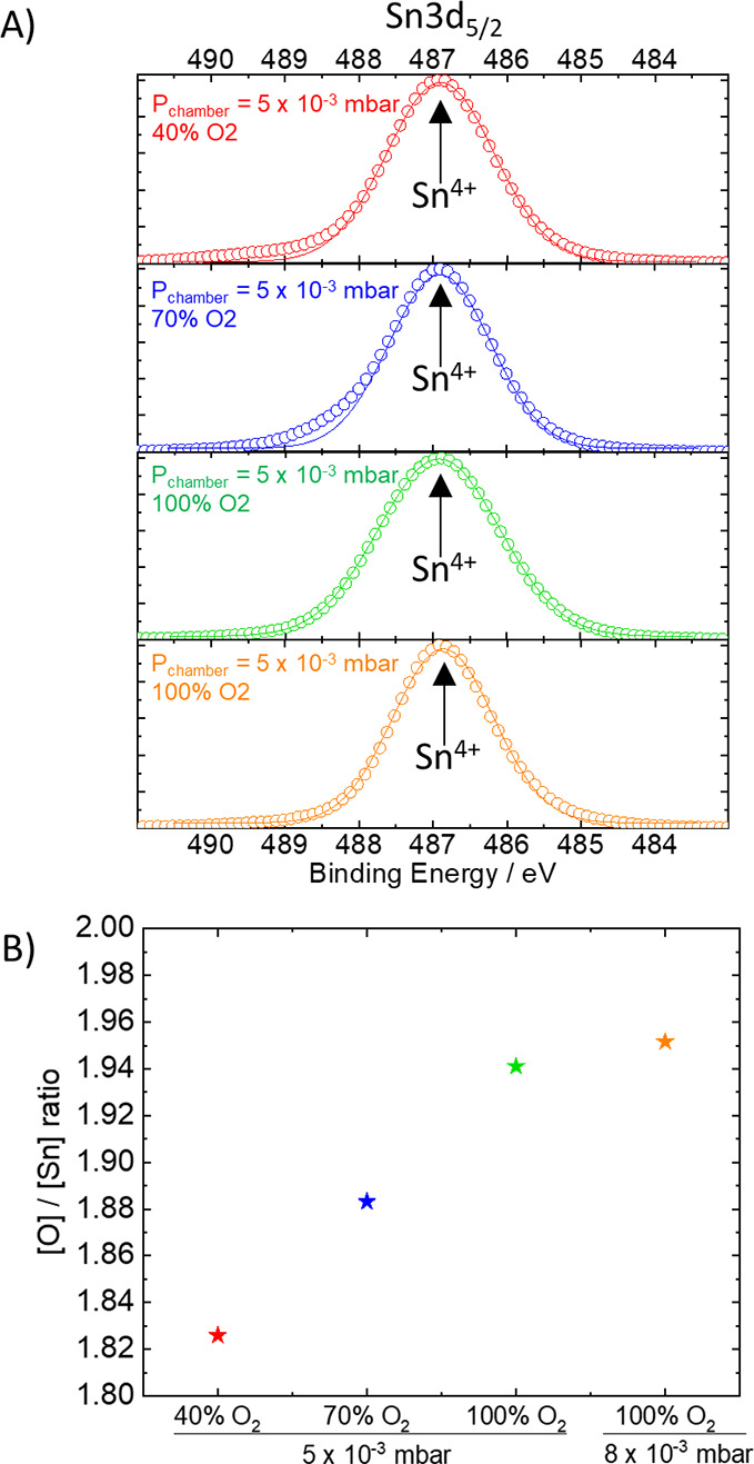
(A) XPS Sn 3d5/2 peaks (in circles) with deconvoluted components (solid lines) and (B) atomic compositions of annealed SnOx layers (20 nm) deposited under different PLD chamber pressures and oxygen concentrations.
Similar to other reported room temperature PLD processes,27,28 the pristine PLD-SnOx films were amorphous, with no peaks to be found in the X-ray diffraction (XRD) pattern (Figure S3). Moreover, even though annealing can be expected to enhance crystallinity of amorphous films, the XRD of the annealed SnOx films also revealed an amorphous nature, as similarly observed by Rucavado et al. for Zn-doped SnO2 annealed at 500 °C.15
Atomic force microscopy (AFM) of the 20 nm SnOx films on glass (Figure 2) revealed very flat surfaces for both films, yet the one deposited at Pchamber at 5.0 × 10⁻³ mbar shows an RMS of around 2.2 nm, homogeneous throughout the whole 5 × 5 μm2 area, while the one deposited at 8.0 × 10⁻³ mbar shows RMS variations from 1.2 nm in the larger area to 7.1 nm in a few smaller regions, with structures that resemble pinholes. Moreover, the presence of occasional undesired particles or debris was not detected in any of the samples as our PLD tool is equipped with a droplet trap to prevent them.
Figure 2.

AFM surface profiles of annealed SnOx films deposited by PLD on glass with a Pchamber of 5.0 × 10⁻³ mbar (A) or 8.0 × 10⁻³ mbar (B).
The transmittance (T), reflectance (R), and absorptance (A = 1– T – R) spectra of the 20 nm SnOx films on glass are depicted in Figure 3. All samples have a high T in the whole visible and near-infrared spectrum (T ≈ 90%), regardless of Pchamber or the O2 concentration, with losses coming mainly from a weak R of ∼10% in the whole spectral range. Because SnOx is a wide bandgap semiconductor, it absorbs light strongly in the ultraviolet region, at wavelengths lower than 320 nm. Based on the Tauc plots, the optical bandgap energies were estimated to be around 3.90 ± 0.01 eV. Additional weak absorptions are observed between 320 and 400 nm, and these absorptions increase proportionally with the amount of VÖ in the films. We therefore ascribe these to the absorption arising from subgap states, as similarly observed elsewhere.15,31
Figure 3.
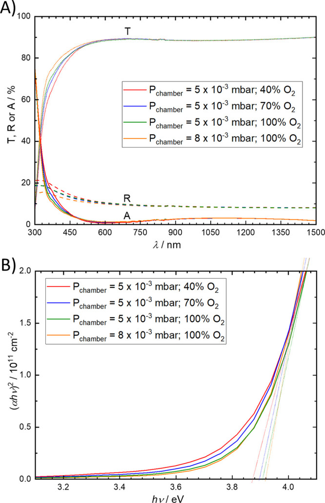
(A) Transmittance (T, ···), reflectance (R, ---), and absorptance (A, −) spectra. (B) Tauc plot of annealed SnOx layers (20 nm) deposited under different PLD chamber pressures and oxygen concentrations.
Despite the occasional subgap states from VÖ, Kelvin probe measurements indicate a similar work function of ∼4.7 eV for all of the investigated samples, regardless of chamber pressure and oxygen partial pressure (Figure S4). This value is in accordance with other reported one for SnO2 films.32,33 Their similar work functions should lead to similar band alignments and Ohmic contacts when these PLD SnO2 films are applied in perovskite solar cells; therefore, any changes in device performance should be accounted for by other factors, for example, the presence of VÖ subgap states.
To evaluate if the VÖ subgap states of the deposited SnOx films can introduce more nonradiative recombination to the perovskite absorber, stacks consisting of glass/ITO/SnOx/MAPbI3 were deposited, and the steady-state photoluminescence (PL) was determined. As is typical of MAPbI3, all samples exhibited a narrow emission band around 770 nm (Figure 4A). As summarized in Figure 4B, the PL quantum yields (PLQY) of the perovskite films with the SnOx films deposited at high O2 concentrations (i.e., with low VÖ) are similar among each other (PLQY ≈ 0.045%); however, the perovskite emission got slightly quenched by the SnOx deposited at the lowest O2 concentration (i.e., with the highest VÖ), reducing the PLQY to 0.037%. This is ascribed to an increased nonradiative recombination through extracted electrons via the VÖ subgap states, which in turn decrease the density of free photogenerated electrons (or quasi-Fermi level splitting, QFLS = VOC,rad + kT ln(PLQY), Figure 4C) in the perovskite.34
Figure 4.

(A) Photoluminescence spectra, (B) PLQY, and (C) QFLS of MAPbI3 perovskite on glass/ITO/SnOx stacks having SnOx layers (20 nm) deposited under different PLD chamber pressures and oxygen concentrations.
We have tried to measure the sheet resistance of our SnO2 thin films either via measurement methods such as van der Pauw or four-probe measurements, but their sheet resistances were beyond the limit of detection of our equipment (>106 Ω/□). It is known that the resistance of undoped oxide semiconductors is very high; for example, Chen et al. have published values as high as 108 Ω/□ for SnO2 thin films similarly deposited by PLD at room temperature,28 in accordance with our own observations. What is typically done instead to obtain information about the conductive properties is to measure the series resistances of devices employing these semiconductor materials, which will be presented in the next section.
SnOx ETL in Perovskite Solar Cells
The developed SnOx films were tested as the ETL in solar cells in the n–i–p configuration, as represented in Figure 5A. This consisted of a glass substrate followed by these layers: ITO (130 nm)/SnOx (20 nm)/C60 (10 nm)/MAPbI3 (500 nm)/TaTm (10 nm)/TPBi (0.5 nm)/MoO3 (7 nm)/Au (100 nm) (where C60 is fullerene, TaTm is N4,N4,N4″,N4″-tetra([1,1′-biphenyl]-4-yl)-[1,1′:4′,1″-terphenyl]-4,4″-diamine, TPBi is 2,2′,2″-(1,3,5-benzinetriyl)-tris(1-phenyl-1H-benzimidazole), and MoO3 is molybdenum(VI) oxide). For comparison, reference devices were also fabricated where SnOx was deposited using ALD instead of PLD (see the Experimental Section for deposition details). The employed architecture relied on C60 and TaTm as intrinsic organic materials for charge selection and SnOx and MoO3 as the charge transport layers for efficient extraction of the photogenerated charge carriers to the external circuit.35 Without the thin C60 layer in between the SnOx and the evaporated perovskite film, we obtained poor fill factors (see the J–V curve of a device, e.g., without C60 in Figure S5). This is in line with our previous observation on solar cells employing solution processed TiO2 charge extraction layers. In that work, very poor performances were obtained when the evaporated perovskite film was deposited directly on the TiO2 layer. This led to poor fill factors and low power conversion efficiency. The insertion of a thin C60 layer alleviated this and led to solar cells reaching PCE’s of 20%.36 Moreover, TPBi was employed to protect TaTm from the diffusion of MoO3, which enables the use of this oxide in n–i–p configuration without compromising the performance or reproducibility of the device.35
Figure 5.

(A) Schematic device architecture, (B) dark J–V curves, (C) external quantum efficiency (EQE) spectra, and (D) illuminated J–V curve (measured under AM 1.5 G irradiation at 100 mW cm–2 at room temperature; forward and reverse scans are presented) of ITO/SnOx/C60/MAPbI3/TaTm/TPBi/MoO3/Au devices with SnOx ETL deposited under different PLD chamber pressures and oxygen concentrations. The represented curves are the average curves of at least 16 samples.
The dark J–V curves for devices containing the developed SnOx ETL are shown in Figure 5B. We note that due to the minimum current range limit of our current meter, the region with current densities lower than 10–4 mA cm–2 (lying around −0.4 to 0.6 V) is poorly resolved. The current density at this voltage range, usually referred as leakage current,37 was very similar (despite the lack of resolution) for samples deposited at 5 × 10⁻³ mbar at all the used oxygen contents; however, it was slightly higher for the device with PLD SnOx deposited at 8 × 10⁻³ mbar. This implies that the pinholes observed in Figure 3 for this sample act as a direct shunt between ITO and C60/perovskite through which the current can leak, leading to parasitic losses in performance when the device is illuminated.37 On the other hand, the dark current density around 1.1 V, dictated by the total series resistance (Rs) in the solar cell,38 was very similar for the devices having PLD SnOx deposited under O2 saturation (100%, either at 5 × 10⁻³ or at 8 × 10⁻³ mbar). As such, the calculated Rs values (Table 1) for these two devices are identical, i.e., 5.8 Ω cm–2. However, as the O2 content during the PLD deposition decreased first to 70% and then to 40%, the current density at this voltage also decreased because of an increase in Rs to 11 and 60 Ω cm–2, respectively. This indicates that the VÖ subgap states observed for the PLD SnOx deposited at low O2 concentrations can decrease the conductivity by trapping the electrons passing through. Finally, the global trend of the dark current density (and calculated Rs) for the devices having PLD SnOx deposited at 5 × 10⁻³ mbar (100% O2) is very similar to that of the reference device that has SnOx deposited via ALD.
Table 1. Photovoltaic Performance of ITO/SnOx/C60/MAPbI3/TaTm/TPBi/MoO3/Au Devices with the SnO2 ETL Deposited under Different PLD Chamber Pressures and Oxygen Concentrationsa.
| SnOx | JSC (mA cm–2) | VOC (V) | FF (%) | PCE (%) | Rs (Ω cm–2)b |
|---|---|---|---|---|---|
| PLD; Pchamber = 5 × 10⁻³ mbar; 40% O2 | 20.2 ± 0.7 | 1.09 ± 0.01 | 28 ± 4 | 5.1 ± 0.9 | 60 ± 8 |
| PLD; Pchamber = 5 × 10⁻³ mbar; 70% O2 | 21.0 ± 0.7 | 1.11 ± 0.01 | 70 ± 4 | 16.4 ± 0.8 | 11 ± 1 |
| PLD; Pchamber = 5 × 10⁻³ mbar; 100% O2 | 21.4 ± 0.3 | 1.11 ± 0.01 | 77 ± 1 | 18.1 ± 0.6 | 5.8 ± 0.7 |
| PLD; Pchamber = 8 × 10⁻³ mbar; 100% O2 | 21.1 ± 0.6 | 1.09 ± 0.01 | 65 ± 6 | 14.9 ± 1.6 | 5.8 ± 0.7 |
| ALD | 21.5 ± 0.3 | 1.11 ± 0.01 | 77 ± 1 | 18.2 ± 0.8 | 4.0 ± 0.8 |
Notation: average ± standard deviation. Number of samples: at least 16 samples for each SnOx.
Calculated from the voltage-independent region of the difference of the light and dark J–V curves using the method described by Grabowski et al.39
The current density versus voltage (J–V curve) under 1 sun illumination for the investigated devices is depicted in Figure 5C (forward and reverse scans are shown), and the photovoltaic parameters are summarized in Table 1. For devices fabricated with the SnOx layer deposited at a chamber pressure of 5 × 10⁻³ mbar under different O2 concentrations, the observed changes in Rs are likely due to the VÖ defect states affecting mostly their fill factor (FF), increasing from 28% to 77% as the O2 concentration during SnOx deposition increased from 40% to 100%, respectively. Another clear effect is on the hysteresis of the curves; typically, fully evaporated flat solar cells have negligible hysteresis, as similarly observed for the sample with SnOx deposited at 100% O2 saturation; however, some hysteresis was observed as the O2 concentration decreased. The open circuit voltage (VOC) reached 1.11 V for devices having SnOx deposited under saturated O2 but decreased slightly to 1.09 V for an O2 concentration of 40%. The trend in VOC is in line with the one observed for the QFLS.40 In a similar fashion, the JSC was higher for the solar cell employing the SnOx film deposited at 100% O2 atmosphere, with 21.4 mA cm–2, and decreased gradually for decreasing amounts of O2 during the SnOx deposition, reaching the lowest value at 20.2 mA cm–2 for 40% O2. As expected, their external quantum efficiency (EQE, Figure 5D) magnitude follows this trend in JSC. The integrated current density from the EQE curves leads to similar values as those for the measured JSC. Even though their EQE profiles were very similar, the device with the SnOx ETL deposited at 40% O2 showed overall a lower EQE value. This is attributed primarily to a reduced charge extraction following the increased Rs due to more oxygen vacancies. Optical effects also played a role at wavelengths lower than 400 nm, in which the increased VÖ subgap states led to additional parasitic absorption (see transmittance spectra in Figure 3).
The PSCs employing the PLD-SnOx deposited under 8 × 10⁻³ mbar (100% O2) showed J–V curves that were virtually free of hysteresis, and the devices showed similar JSC and EQE to the one fabricated at 5 × 10⁻³ mbar (100% O2). However, their VOC and FF are slightly lower as a possible consequence of the aforementioned shunts, through which the leakage current can flow in parallel to the photocurrent.37
The best performance of the PSC was achieved with a SnOx layer deposited at 5 × 10⁻³ mbar and 100% O2, leading to a PCE of 18.2%. This performance is on par with that of the reference devices fabricated with ALD SnOx, which is well-known for leading to flat pinhole-free SnOx layers and reproducible performances,10,11,41,42 proving the quality of our PLD films. The PLD process is much faster than ALD and can be done on larger areas and industrial scales, but perhaps the main advantage over ALD is that PLD allows the use of shadow masks for patterning, which can make the widespread use of SnOx ETLs even more appealing.
Conclusions
In conclusion, we demonstrated that the PLD deposition of SnOx electron transport layers should be performed under O2-saturated conditions in order to reduce the formation of oxygen vacancies. This leads to lower parasitic absorption and low resistivity. Crucial to avoid shunts or even shortened devices, flat pinhole-free surfaces with nanometric roughness and no debris can be obtained with deposition pressures of 5 × 10⁻³ mbar. Using the optimum SnOx film, planar n–i–p perovskite solar cells can reach power conversion efficiencies exceeding 18%, with similar PCE to a reference device employing ALD deposited SnOx. Because of the superior deposition speed, low material consumption, the possibility to use shadow mask, and proven scalability, the PLD process holds more promise for industrialization.
Experimental Section
TaTm was provided by TCI. C60 was purchased from Sigma-Aldrich. PbI2 was purchased from Tokyo Chemical Industry CO. MoO3, TPBi, and methylammonium iodide (MAI) were purchased from Lumtec.
Prepatterned ITO-coated glass substrates were purchased from Naranjo Substrates. They were cleaned by subsequent immersions in soap, water, deionized water, and isopropanol in a sonication bath for 5 min each, followed by insertion in an ozone chamber with UV irradiation for 20 min.
Industrial Scale PLD System
The SnOx films were deposited at room temperature using a Solmates large area PLD 200 mm system. This PLD tool was coupled to a N2 glovebox to minimize any detrimental effects from the presence of O2 and moisture on the performance of the finally produced devices. A Lightmachinery’s IPEX-700 KrF excimer laser (λ = 248 nm) was employed, setting the repetition rate at 25 Hz and a fluence of 1.5–1.6 J cm–2. The source material for SnO2 deposition was an SnO2 ceramic target (99.9%), acquired from Pi-kem. The substrates were allocated 90 mm on top of the target. The system was equipped with a droplet trap to reduce the number of undesired particles on the deposited film, which allowed for a homogeneous deposition on large areas >615 cm2, with less than 1.5% variation in TCO thickness and sheet resistance. The droplet trap consisted of a large metal disk, with only four round openings at 90° from each other. The droplet trap was located between the target and the substrates, rotating at a speed of 3000 rpm. The laser was synchronized with the rotation of the disk, so that the laser can hit the target when the opening was directly above the target; in that way, the generated plasma plume can pass through the opening and reach the substrate. Any particle or drop generated slightly later will be blocked by the metal disk as the opening has moved away.
Device Fabrication
The solar cell layers were prepared by vacuum sublimation of the entire solar cell stack on glass/ITO/PLD-SnOx substrates. The substrates were 3 × 3 cm2 and contained 16 rectangular working pixels, each pixel with an approximate area of 0.082 cm2, with a similar layout to the one published recently;27 all the samples were irradiated from the glass side using an illumination mask positioned at the center of the pixels with an opening of precise 0.050 cm2. Thermal vacuum deposition was performed in vacuum chambers evacuated to a pressure of 10–6 mbar, which were integrated into a nitrogen-filled glovebox (H2O and O2 < 0.1 ppm). In general, the vacuum chambers were equipped with temperature-controlled evaporation sources (Creaphys) fitted with ceramic crucibles. The sources were directed upward with an angle of approximately 90° with respect to the base of the evaporator. The distance between the substrate holder and the evaporation source was approximately 30 cm. Individual quartz crystal microbalance (QCM) sensors monitored the deposition rate of each evaporation source, and another one close to the substrate holder monitored the total deposition rate. For the perovskite deposition, MAI and PbI2 were coevaporated at the same time by measuring the deposition rate of each material in two QCM sensors and obtaining the total perovskite thickness in a third one located closer to the substrates, leading to a 500 nm thick perovskite. TaTm, C60, and TPBi were sublimed in the same vacuum chamber with temperatures around 300, 400, and 200 °C, respectively, to a precise desired thickness. MoO3 and Ag were evaporated in another vacuum chamber using tungsten boats as sources by applying currents ranging from 2.0 to 4.5 A. For the reference devices, a 20 nm layer of SnOx was deposited by ALD following a procedure recently published by us43 using an Arradiance’s GEMStar XT Thermal ALD system integrated into a nitrogen-filled glovebox. In summary, the ALD chamber was heated to 90 °C, the bottle containing the Sn precursor (tetrakis(dimethylamino)tin, TDAT) was heated to 60 °C, and the bottle of the oxidizer (water) was not heated; the precursor and oxidizer manifolds were heated to 115 and 140 °C, respectively. Prior to deposition, the tubes and valves in the manifolds were degassed three times by performing a series of 30 pulses with the bottles manually closed. The ALD cycle consisted of consecutive purges of TDAT for 550 ms and water vapor for 200 ms, each followed by N2 purges of 30 and 105 s, respectively, to ensure the complete removal of the precursors from the ALD chamber. All the devices showed here, with either PLD or ALD SnO2, were encapsulated using ALD of Al2O3 at 40 °C, using a protocol recently published by us.44
General Characterization
T, R, and A spectra between 300 and 1500 nm were collected using a PerkinElmer Lambda 950 UV–vis–NIR spectrophotometer, coupled with an integrating sphere; by assuming a direct band gap transition and a thickness of 20 nm, the optical band gap of these materials was then estimated using Tauc plot analysis. XPS spectra were recorded using a Thermo Scientific K-Alpha with a monochromatic Al Kα X-ray source (1486.6 eV); data were analyzed and deconvoluted with Avantage software, and the binding energies were adjusted to the standard C 1s peak at 284.6 eV. Thicknesses were measured with an Ambios XP1 mechanical profilometer. X-ray diffraction was measured with a Panalytical Empyrean diffractometer equipped with a Cu Kα anode operated at 45 kV and 30 mA and a Pixel 1D detector in scanning line mode; single scans were acquired in the 2θ = 5°–50° range in Bragg–Brentano geometry in air. AFM of sample surfaces was obtained using a Bruker ICON Dimension microscope in tapping mode. Work function measurements were obtained by using a KP Technology Air Photoemission and Kelvin Probe system.
The external quantum efficiency (EQE) was estimated using the cell response at different wavelengths (measured with a white light halogen lamp in combination with band-pass filters). A possible solar spectrum mismatch was checked with a calibrated silicon reference cell (MiniSun simulator by ECN, from Netherlands) by means of the correction methodology published by NREL.45 The J–V curves for the solar cells were recorded using a Keithley 2612A SourceMeter in −0.2 and 1.2 V voltage range with 0.01 V steps and integrating the signal for 20 ms after a 10 ms delay, corresponding to a speed of about 0.3 V s–1. The devices were illuminated under a Wavelabs Sinus 70 AAA LED solar simulator. The light intensity was calibrated before every measurement using a calibrated Si reference diode equipped with an infrared cutoff filter (KG-3, Schott). For all devices, we compared the calculated JSC from the EQE with that obtained from the J–V analysis of the cells illuminated with the AAA Led solar simulator. During experiments, the encapsulated devices were exposed to air, and temperature was stabilized at 298 K using a cooling system controlled by a Peltier element.
Acknowledgments
The authors gratefully acknowledge financial support of the European Research Council (ERC) under the European Union’s Horizon 2020 research and innovation programme (Grant agreement No. 834431). The authors acknowledge support from the Comunitat Valenciana: H.B. for projects IDIFEDER/2018/061 and PROMETEU/2020/077; M.S. for project CISEJI/2022/43; K.P.S.Z. for project APOSTD/2021/368. The authors also acknowledge support by the Ministry of Science and Innovation (MCIN) and the Spanish State Research Agency (AEI): Grant PDC2021-121317-I00 funded by MCIN/AEI/10.13039/501100011033 and by the “European Union NextGenerationEU/PRTR”; grants PRE2019-091181 and RYC-2016-21316 funded by MCIN/AEI/10.13039/501100011033 and by “ESF Investing in your future”; Project CEX2019-000919-M funded by MCIN/AEI/10.13039/501100011033; K.P.S.Z. for a Juan de la Cierva scholarship (IJC2020-045130-I). Finally, W.S. and M.M.M. acknowledge the support from the Solar-ERA.NET CUSTCO project by The Netherlands Enterprise Agency (RVO) under Contract SOL18001.
Supporting Information Available
The Supporting Information is available free of charge at https://pubs.acs.org/doi/10.1021/acsami.3c04387.
Additional J–V curves, XPS spectra, and XRD pattern (PDF)
The authors declare no competing financial interest.
Supplementary Material
References
- Lee M. M.; Teuscher J.; Miyasaka T.; Murakami T. N.; Snaith H. J. Efficient Hybrid Solar Cells Based on Meso-Superstructured Organometal Halide Perovskites. Science 2012, 338, 643–647. 10.1126/science.1228604. [DOI] [PubMed] [Google Scholar]
- Shi Z.; Jayatissa A. Perovskites-Based Solar Cells: A Review of Recent Progress, Materials and Processing Methods. Materials 2018, 11, 729. 10.3390/ma11050729. [DOI] [PMC free article] [PubMed] [Google Scholar]
- Lin L.; Jones T. W.; Yang T. C.; Duffy N. W.; Li J.; Zhao L.; Chi B.; Wang X.; Wilson G. J. Inorganic Electron Transport Materials in Perovskite Solar Cells. Adv. Funct. Mater. 2021, 31, 2008300. 10.1002/adfm.202008300. [DOI] [Google Scholar]
- Mao G.-P.; Wang W.; Shao S.; Sun X.-J.; Chen S.-A.; Li M.-H.; Li H.-M. Correction To: Research Progress In Electron Transport Layer In Perovskite Solar Cells. Rare Met. 2020, 10.1007/s12598-020-01375-8. [DOI] [Google Scholar]
- Snaith H. J.; Ducati C. SnO2-Based Dye-Sensitized Hybrid Solar Cells Exhibiting Near Unity Absorbed Photon-to-Electron Conversion Efficiency. Nano Lett. 2010, 10, 1259–1265. 10.1021/nl903809r. [DOI] [PubMed] [Google Scholar]
- Tiwana P.; Docampo P.; Johnston M. B.; Snaith H. J.; Herz L. M. Electron Mobility and Injection Dynamics in Mesoporous ZnO, SnO2, and TiO2 Films Used in Dye-Sensitized Solar Cells. ACS Nano 2011, 5, 5158–5166. 10.1021/nn201243y. [DOI] [PubMed] [Google Scholar]
- Das S.; Jayaraman V. SnO2: A Comprehensive Review On Structures And Gas Sensors. Prog. Mater. Sci. 2014, 66, 112–255. 10.1016/j.pmatsci.2014.06.003. [DOI] [Google Scholar]
- Ke W.; Fang G.; Liu Q.; Xiong L.; Qin P.; Tao H.; Wang J.; Lei H.; Li B.; Wan J.; Yang G.; Yan Y. Low-Temperature Solution-Processed Tin Oxide as an Alternative Electron Transporting Layer for Efficient Perovskite Solar Cells. J. Am. Chem. Soc. 2015, 137, 6730–6733. 10.1021/jacs.5b01994. [DOI] [PubMed] [Google Scholar]
- Ren X.; Yang D.; Yang Z.; Feng J.; Zhu X.; Niu J.; Liu Y.; Zhao W.; Liu S. F. Solution-Processed Nb:SnO2 Electron Transport Layer for Efficient Planar Perovskite Solar Cells. ACS Appl. Mater. Interfaces 2017, 9, 2421–2429. 10.1021/acsami.6b13362. [DOI] [PubMed] [Google Scholar]
- Uddin A.; Yi H. Progress and Challenges of SnO2 Electron Transport Layer for Perovskite Solar Cells: A Critical Review. Sol. RRL 2022, 6, 2100983. 10.1002/solr.202100983. [DOI] [Google Scholar]
- Correa Baena J. P.; Steier L.; Tress W.; Saliba M.; Neutzner S.; Matsui T.; Giordano F.; Jacobsson T. J.; Srimath Kandada A. R.; Zakeeruddin S. M.; Petrozza A.; Abate A.; Nazeeruddin M. K.; Grätzel M.; Hagfeldt A. Highly Efficient Planar Perovskite Solar Cells Through Band Alignment Engineering. Energy Environ. Sci. 2015, 8, 2928–2934. 10.1039/C5EE02608C. [DOI] [Google Scholar]
- Xiong L.; Guo Y.; Wen J.; Liu H.; Yang G.; Qin P.; Fang G. Review on the Application of SnO2 in Perovskite Solar Cells. Adv. Funct. Mater. 2018, 28, 1802757. 10.1002/adfm.201802757. [DOI] [Google Scholar]
- Tan C.; Xu W.; Huan Y.; Wu B.; Qin T.; Gao D. Increasing Stability of SnO2 -Based Perovskite Solar Cells by Introducing an Anionic Conjugated Polyelectrolyte for Interfacial Adjustment. ACS Appl. Mater. Interfaces 2021, 13, 24575–24581. 10.1021/acsami.1c00410. [DOI] [PubMed] [Google Scholar]
- Park S. Y.; Zhu K. Advances in SnO2 for Efficient and Stable n–i–p Perovskite Solar Cells. Adv. Mater. 2022, 34, 2110438. 10.1002/adma.202110438. [DOI] [PubMed] [Google Scholar]
- Rucavado E.; Jeangros Q.; Urban D. F.; Holovský J.; Remes Z.; Duchamp M.; Landucci F.; Dunin-Borkowski R. E.; Körner W.; Elsässer C.; Hessler-Wyser A.; Morales-Masis M.; Ballif C. Enhancing The Optoelectronic Properties Of Amorphous Zinc Tin Oxide By Subgap Defect Passivation: A Theoretical And Experimental Demonstration. Phys. Rev. B 2017, 95, 245204. 10.1103/PhysRevB.95.245204. [DOI] [Google Scholar]
- Jayaraj M. K.; Saji K. J.; Nomura K.; Kamiya T.; Hosono H. Optical And Electrical Properties Of Amorphous Zinc Tin Oxide Thin Films Examined For Thin Film Transistor Application. J. Vac. Sci. Technol. B Microelectron. Nanom. Struct. 2008, 26, 495. 10.1116/1.2839860. [DOI] [Google Scholar]
- Körner W.; Gumbsch P.; Elsässer C. Analysis Of Electronic Subgap States In Amorphous Semiconductor Oxides Based On The Example Of Zn-Sn-O Systems. Phys. Rev. B 2012, 86, 165210. 10.1103/PhysRevB.86.165210. [DOI] [Google Scholar]
- Körner W.; Urban D. F.; Elsässer C. Generic Origin Of Subgap States In Transparent Amorphous Semiconductor Oxides Illustrated For The Cases Of In-Zn-O and In-Sn-O. Phys. Status Solidi 2015, 212, 1476–1481. 10.1002/pssa.201431871. [DOI] [Google Scholar]
- Körner W.; Elsässer C. Density-Functional Theory Study Of Stability And Subgap States Of Crystalline And Amorphous Zn–Sn–O. Thin Solid Films 2014, 555, 81–86. 10.1016/j.tsf.2013.05.146. [DOI] [Google Scholar]
- Kröger F. A.; Vink H. J. Relations Between The Concentrations Of Imperfections In Solids. J. Phys. Chem. Solids 1958, 5, 208–223. 10.1016/0022-3697(58)90069-6. [DOI] [Google Scholar]
- Wu P.; Wang S.; Li X.; Zhang F. Advances In Sno2 -Based Perovskite Solar Cells: From Preparation To Photovoltaic Applications. J. Mater. Chem. A 2021, 9, 19554–19558. 10.1039/D1TA04130D. [DOI] [Google Scholar]
- Huang S.; Li P.; Wang J.; Huang J. C.-C.; Xue Q.; Fu N. Modification of SnO2 Electron Transport Layer: Brilliant Strategies To Make Perovskite Solar Cells Stronger. Chem. Eng. J. 2022, 439, 135687. 10.1016/j.cej.2022.135687. [DOI] [Google Scholar]
- Morales-Paliza M. A.; Haglund R. F.; Feldman L. C. Mechanisms Of Oxygen Incorporation In Indium–Tin–Oxide Films Deposited By Laser Ablation At Room Temperature. Appl. Phys. Lett. 2002, 80, 3757–3759. 10.1063/1.1481243. [DOI] [Google Scholar]
- Smirnov Y.; Schmengler L.; Kuik R.; Repecaud P.; Najafi M.; Zhang D.; Theelen M.; Aydin E.; Veenstra S.; De Wolf S.; Morales-Masis M. Scalable Pulsed Laser Deposition of Transparent Rear Electrode for Perovskite Solar Cells. Adv. Mater. Technol. 2021, 6, 2000856. 10.1002/admt.202000856. [DOI] [Google Scholar]
- Aydin E.; Altinkaya C.; Smirnov Y.; Yaqin M. A.; Zanoni K. P. S.; Paliwal A.; Firdaus Y.; Allen T. G.; Anthopoulos T. D.; Bolink H. J.; Morales-Masis M.; De Wolf S. Sputtered Transparent Electrodes For Optoelectronic Devices: Induced Damage And Mitigation Strategies. Matter 2021, 4, 3549–3584. 10.1016/j.matt.2021.09.021. [DOI] [Google Scholar]
- Smirnov Y.; Repecaud P.-A.; Tutsch L.; Florea I.; Zanoni K. P. S.; Paliwal A.; Bolink H. J.; Cabarrocas P. R.; Bivour M.; Morales-Masis M. Wafer-Scale Pulsed Laser Deposition Of ITO For Solar Cells: Reduced Damage Vs. Interfacial Resistance. Mater. Adv. 2022, 3, 3469–3478. 10.1039/D1MA01225H. [DOI] [Google Scholar]
- Zanoni K. P. S.; Paliwal A.; Hernández-Fenollosa M. A.; Repecaud P.; Morales-Masis M.; Bolink H. J. ITO Top-Electrodes via Industrial-Scale PLD for Efficient Buffer-Layer-Free Semitransparent Perovskite Solar Cells. Adv. Mater. Technol. 2022, 7, 2101747. 10.1002/admt.202101747. [DOI] [Google Scholar]
- Chen Z.; Yang G.; Zheng X.; Lei H.; Chen C.; Ma J.; Wang H.; Fang G. Bulk Heterojunction Perovskite Solar Cells Based On Room Temperature Deposited Hole-Blocking Layer: Suppressed Hysteresis And Flexible Photovoltaic Application. J. Power Sources 2017, 351, 123–129. 10.1016/j.jpowsour.2017.03.087. [DOI] [Google Scholar]
- Kwoka M.; Ottaviano L.; Passacantando M.; Santucci S.; Czempik G.; Szuber J. XPS Study Of The Surface Chemistry Of L-CVD Sno2 Thin Films After Oxidation. Thin Solid Films 2005, 490, 36–42. 10.1016/j.tsf.2005.04.014. [DOI] [Google Scholar]
- Lu F.; Ji X.; Yang Y.; Deng W.; Banks C. E. Room Temperature Ionic Liquid Assisted Well-Dispersed Core-Shell Tin Nanoparticles Through Cathodic Corrosion. RSC Adv. 2013, 3, 18791–18793. 10.1039/c3ra43532f. [DOI] [Google Scholar]
- Rucavado E.; Graužinytė M.; Flores-Livas J. A.; Jeangros Q.; Landucci F.; Lee Y.; Koida T.; Goedecker S.; Hessler-Wyser A.; Ballif C.; Morales-Masis M. New Route for “Cold-Passivation” of Defects in Tin-Based Oxides. J. Phys. Chem. C 2018, 122, 17612–17620. 10.1021/acs.jpcc.8b02302. [DOI] [PMC free article] [PubMed] [Google Scholar]
- Islam M. N.; Hakim M. O. Electron Affinity And Work Function Of Polycrystalline Sno2 Thin Film. J. Mater. Sci. Lett. 1986, 5, 63–65. 10.1007/BF01671438. [DOI] [Google Scholar]
- Ganose A. M.; Scanlon D. O. Band Gap And Work Function Tailoring Of Sno2 For Improved Transparent Conducting Ability In Photovoltaics. J. Mater. Chem. C 2016, 4, 1467–1475. 10.1039/C5TC04089B. [DOI] [Google Scholar]
- Kirchartz T.; Rau U. Detailed Balance And Reciprocity In Solar Cells. Phys. status solidi 2008, 205, 2737–2751. 10.1002/pssa.200880458. [DOI] [Google Scholar]
- Pérez-del-Rey D.; Gil-Escrig L.; Zanoni K. P. S.; Dreessen C.; Sessolo M.; Boix P. P.; Bolink H. J. Molecular Passivation of MoO3: Band Alignment and Protection of Charge Transport Layers in Vacuum-Deposited Perovskite Solar Cells. Chem. Mater. 2019, 31, 6945–6949. 10.1021/acs.chemmater.9b01396. [DOI] [Google Scholar]
- Pérez-del-Rey D.; Boix P. P.; Sessolo M.; Hadipour A.; Bolink H. J. Interfacial Modification for High-Efficiency Vapor-Phase-Deposited Perovskite Solar Cells Based on a Metal Oxide Buffer Layer. J. Phys. Chem. Lett. 2018, 9, 1041–1046. 10.1021/acs.jpclett.7b03361. [DOI] [PubMed] [Google Scholar]
- Proctor C. M.; Nguyen T.-Q. Effect Of Leakage Current And Shunt Resistance On The Light Intensity Dependence Of Organic Solar Cells. Appl. Phys. Lett. 2015, 106, 083301. 10.1063/1.4913589. [DOI] [Google Scholar]
- Mundhaas N.; Yu Z. J.; Bush K. A.; Wang H.; Häusele J.; Kavadiya S.; McGehee M. D.; Holman Z. C. Series Resistance Measurements of Perovskite Solar Cells Using Jsc – Voc Measurements. Sol. RRL 2019, 3, 1800378. 10.1002/solr.201800378. [DOI] [Google Scholar]
- Grabowski D.; Liu Z.; Schöpe G.; Rau U.; Kirchartz T. Fill Factor Losses and Deviations from the Superposition Principle in Lead Halide Perovskite Solar Cells. Sol. RRL 2022, 6, 2200507. 10.1002/solr.202200507. [DOI] [Google Scholar]
- Caprioglio P.; Stolterfoht M.; Wolff C. M.; Unold T.; Rech B.; Albrecht S.; Neher D. On the Relation between the Open-Circuit Voltage and Quasi-Fermi Level Splitting in Efficient Perovskite Solar Cells. Adv. Energy Mater. 2019, 9, 1901631. 10.1002/aenm.201901631. [DOI] [Google Scholar]
- Wang C.; Zhao D.; Grice C. R.; Liao W.; Yu Y.; Cimaroli A.; Shrestha N.; Roland P. J.; Chen J.; Yu Z.; Liu P.; Cheng N.; Ellingson R. J.; Zhao X.; Yan Y. Low-Temperature Plasma-Enhanced Atomic Layer Deposition Of Tin Oxide Electron Selective Layers For Highly Efficient Planar Perovskite Solar Cells. J. Mater. Chem. A 2016, 4, 12080–12087. 10.1039/C6TA04503K. [DOI] [Google Scholar]
- Wang C.; Xiao C.; Yu Y.; Zhao D.; Awni R. A.; Grice C. R.; Ghimire K.; Constantinou I.; Liao W.; Cimaroli A. J.; Liu P.; Chen J.; Podraza N. J.; Jiang C.; Al-Jassim M. M.; Zhao X.; Yan Y. Understanding and Eliminating Hysteresis for Highly Efficient Planar Perovskite Solar Cells. Adv. Energy Mater. 2017, 7, 1700414. 10.1002/aenm.201700414. [DOI] [Google Scholar]
- Wang C.; Xiao C.; Yu Y.; Zhao D.; Awni R. A.; Grice C. R.; Ghimire K.; Constantinou I.; Liao W.; Cimaroli A. J.; Liu P.; Chen J.; Podraza N. J.; Jiang C.-S.; Al-Jassim M. M.; Zhao X.; Yan Y. Understanding and Eliminating Hysteresis for Highly Efficient Planar Perovskite Solar Cells. Energy Technol. 2017, 7, 1700414. 10.1002/aenm.201700414. [DOI] [Google Scholar]
- Kaya I. C.; Zanoni K. P. S.; Palazon F.; Sessolo M.; Akyildiz H.; Sonmezoglu S.; Bolink H. J. Crystal Reorientation and Amorphization Induced by Stressing Efficient and Stable p-i-n Vacuum-Processed MAPbI3 Perovskite Solar Cells. Adv. Energy Sustain. Res. 2021, 2, 2000065. 10.1002/aesr.202000065. [DOI] [Google Scholar]
- Available in www.nrel.gov/pv/text-spectral-mismatch-corrections.html, accessed on 2022-11-14.
Associated Data
This section collects any data citations, data availability statements, or supplementary materials included in this article.