Abstract
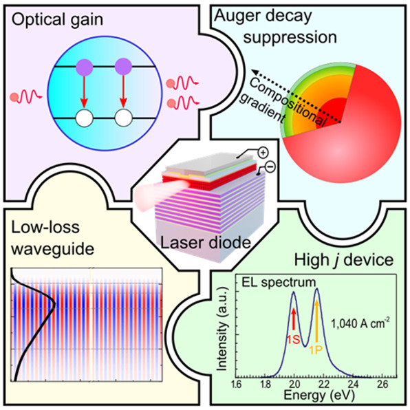
Lasers and optical amplifiers based on solution-processable materials have been long-desired devices for their compatibility with virtually any substrate, scalability, and ease of integration with on-chip photonics and electronics. These devices have been pursued across a wide range of materials including polymers, small molecules, perovskites, and chemically prepared colloidal semiconductor nanocrystals, also commonly referred to as colloidal quantum dots. The latter materials are especially attractive for implementing optical-gain media as in addition to being compatible with inexpensive and easily scalable chemical techniques, they offer multiple advantages derived from a zero-dimensional character of their electronic states. These include a size-tunable emission wavelength, low optical gain thresholds, and weak sensitivity of lasing characteristics to variations in temperature. Here we review the status of colloidal nanocrystal lasing devices, most recent advances in this field, outstanding challenges, and the ongoing progress toward technological viable devices including colloidal quantum dot laser diodes.
1. Introduction
Present-day semiconductor lasers are based on optical gain media that comprise one or multiple thin, atomically defined semiconductor layers or “quantum wells” grown by vacuum-based epitaxial techniques.1 The quantum wells are usually made of binary, ternary, or quaternary combinations of III-V semiconductors. For example, compounds such as InxGa1–xN and (AlxGa1–x)1–yInyP are used for lasing in the visible spectral range,2,3 while materials such as InxGa1–xAs and GaxIn1–xAsySb1–y are employed for lasing in the range of infrared (IR) wavelengths.4,5 Commonly, the semiconductor gain medium is excited electrically, which is accomplished by incorporating it into a charge injection architecture similar to that of a traditional light emitting diode (LED). These devices, termed laser diodes, are highly efficient and can produce power outputs of up to hundreds of Watts in a wide range of wavelengths from the IR6 to the ultraviolet (UV).7 The breadth of available performance characteristics in combination with the simplicity of electrical pumping make laser diodes the most widely used laser devices.
While traditional laser diodes satisfy many existing needs, there are certain areas that would be better served by lasers based on solution-processable materials. In particular, there is a considerable need for lasers and optical amplifiers that could be readily integrated with silicon technologies. This would open the door to very large-scale integration (VLSI) in microelectronics,8 simplify integration of photonic and electronic circuits,9 and allow for on-chip implementation of photon-based quantum information and communication schemes.10 The integration of the existing III-V lasers and amplifiers with Si-based microelectronic devices is notoriously difficult due to material incompatibility issues. Therefore, present-day solutions entail either off-chip or wafer-bonded lasers/amplifiers.11 This complicates the fabrication cycle, greatly limits the system complexity, and increases the cost. Other areas that would greatly benefit from the availability of solution-processable lasing devices include lab-on-a-chip platforms,12 wearable devices,13 and advanced medical diagnostics.14
In addition to enabling future advances across a diverse range of technologies, the use of solution-processable systems could simplify the fabrication protocols by eliminating the need for a clean-room environment, removing stringent lattice-matching requirements, and expanding the palette of materials used as both lasing media and underlying substrate or embedding matrix. Importantly, as in present-day colloidal quantum dot (QD) LEDs, in prospective QD laser diodes, an entire device stack can be assembled on an inexpensive substrate (made of, e.g., glass or plastic) using low-cost high-throughput techniques such as spin-coating or inkjet printing supplemented by standard thermal evaporation (for, e.g., application of contacts).15−17 This is expected to lead to a dramatic cost reduction compared to epitaxial devices, especially in the case of large-area structures.18,19
Several systems have been under investigation in the context of solution-processable solid-state lasers. These include organic semiconducting polymers and small molecules,20 solution-grown semiconductor nanowires,21 as well as organic–inorganic (“hybrid”) and all-inorganic perovskite prepared as bulk films22,23 or nanostructures with different form factors.24,25 All of these systems achieved lasing with optical excitation; however, realization of the lasing effect with electrical pumping has been challenging. Among organic materials, the most successful system has been, perhaps, 4,4′-bis[(N-carbazole) styryl]biphenyl (BSBCz).26 Optical gain media made of these molecules exhibited low amplified spontaneous emission (ASE) thresholds27 and featured good stability in short-pulse electroluminescent (EL) devices up to very high current densities of ∼3 kA cm–2.28 Recently, BSBCz molecules were used to realize devices that showed the emergence of coherent laser emission mixed with incoherent EL.28
A promising class of solution-processable gain media is semiconductor nanocrystals fabricated using benchtop colloidal techniques.15,29−32 As prepared, nanocrystals comprise a nanosized semiconductor core overcoated with a shell of organic molecules. Due to the presence of both organic and inorganic structural components, colloidal nanocrystals combine chemical flexibility of molecular structures with advantages of well-understood inorganic semiconductors. In particular, they can be chemically manipulated as large molecules, which simplifies their integration with photonic and electronic structures without restrictions imposed by lattice-match requirements or the need for costly vacuum-based fabrication techniques. At the same time, they exhibit beneficial features of quantum-confined inorganic semiconductors such as high chemical and environment stability and a size-dependent bandgap. The latter property allows one to continuously tune their emission spectrum across a wide range of wavelengths and, in particular, fill spectral gaps not covered with the existing lasers. Importantly, semiconductor nanocrystals maintain high emission efficiencies from the UV, throughout the visible and to the IR spectral range.33−35 This is a favorable distinction from, for example, organic molecules that are very poor IR emitters.36 In addition, a wide separation between nanocrystal atomic-like electronic states inhibits thermal depopulation of the light-emitting band-edge levels, which reduces optical-gain and lasing thresholds compared to bulk materials and improves temperature stability of lasing characteristics.32,37
Modern colloidal techniques allow for atomic-level control of nanocrystal dimensions, shape, and internal structure.38−41 Nanocrystals can exhibit a variety of morphologies such as “nanospheres”,42 “nanocubes”,43,44 elongated “nanorods”,45 flat “nanoplatelets” (NPLs),46,47 branched “tetrapods”,48 and “spherical quantum wells”.49−51 If all three dimensions of a nanocrystal are “quantum-confined,” it can be treated as a zero-dimensional (0D) structure, often referred to as a “quantum dot”, independent of its exact shape. Sufficiently long nanorods exhibit properties of 1D structures, while large-area NPLs are akin to 2D quantum wells. Thus, colloidal nanomaterials allow one to access all three confinement regimes: 0D, 1D, and 2D.
Nowadays, semiconductor nanocrystals are not just the subject of scientific curiosity but mature technological-grade materials that can be found in commercial products such as displays and television sets. Presently, most of the nanocrystal applications exploit their excellent light-emitting properties stemming from high-emission efficiencies, size-controlled emission colors, and narrow emission linewidths. There is also a considerable potential for nanocrystals as optical gain materials for implementing color-selectable lasers processed from solutions.15,29−32 In fact, semiconductor nanocrystals were the first class of 0D nanostructures that demonstrated the lasing effect.52 These pioneering experiments were conducted in the early 1990s using CdSe nanocrystals prepared by high-temperature precipitation in molten glasses.53 When incorporated into a Fabry–Pérot cavity, the nanocrystal sample showed lasing at the band-edge transition which was displaced by more than 100 meV from the bulk bandgap due to quantum-confinement effects.
Despite the success of these early experiments, the realization of lasing with colloidal nanocrystals encountered several problems, one of which was an expected detrimental influence of nonradiative Auger decay, whose rate was extremely fast in small-size colloidal particles.54 Eventually these challenges were resolved, and amplified spontaneous emission (ASE)– a precursor of lasing – was realized with colloidal CdSe QDs.29 An important result of these studies was the demonstration of ASE at 2.3 eV (at temperature T = 80 K). This corresponded to the green color as opposed to the deep-red emission due to the band-edge transition of bulk CdSe (∼1.83 eV at T = 80 K). This indicated a very large confinement-induced bandgap shift of almost 500 meV.
Despite more than two decades of research, nanocrystal lasing is still not at the stage of commercial products. As in the early days of lasing research, the progress has been impeded by fast Auger recombination of optical-gain-active multiexciton states and the related difficulties for realizing lasing with continuous wave (cw) optical and electrical excitation. Recently, there has been considerable progress in the development of approaches for highly effective control of Auger decay using methods such as stepwise or continuous compositional grading of the nanocrystal interior.55−59 These new developments have led to several important advances in the nanocrystal lasing field, which include the demonstration of optically pumped cw colloidal QD lasers,60 the realization of subsingle-exciton lasing with charged QDs,61 the demonstration of optical gain regime with electrical injection,16,59 and the development of dual-function devices that operate as an ultrahigh-current-density LED and an optically excited laser.62 An important recent breakthrough is the realization of electrically pumped ASE light sources based on colloidall QDs.63 The development of these devices opens tremendous opportunities across multiple fields from general laser technologies to emerging areas of on-chip photonics64 and plasmonics,65 optical interconnects for high-performance computing,66 and biosensing.67
There have been a number of reviews devoted to fundamental and applied aspects of nanocrystal lasing.15,30−32,68 The purpose of the present review is to focus on the most recent advances in this field and to discuss the outstanding challenges and prospects of nanocrystal lasing technologies. Specific topics covered in this review include general principles of nanocrystal lasing, advanced optical gain concepts, emerging nanocrystal-based optical gain materials, and fundamental and applied aspects of nanocrystal laser diodes. Among the newest developments overviewed here are the recent implementation of a “charged-exciton” gain concept with chemically treated PbS nanocrystals for lasing in the range of IR wavelengths, the demonstration of sub-bandgap lasing due to Auger-assisted stimulated emission, the new low-optical-loss charge-injection architectures for light amplification devices, and the realization of ASE with electrical excitation using nanocrystal LEDs with an integrated photonic waveguide.
2. General Principles of Nanocrystal Lasing
2.1. Electronic States in Semiconductor Nanocrystals
A characteristic length scale of electronic excitations in macroscopic semiconductor crystals is defined by the exciton Bohr radius, ax. If one of the dimensions of a nanocrystal is comparable to or smaller than ax, its electronic energies become dependent on the particle size, which is known as the quantum-size effect. By exploiting this phenomenon, it is possible to tune the nanocrystal bandgap (Eg), which yields a powerful tool for wide-range tuning of the emission energy of nanocrystal materials.
Another characteristic feature of small-size nanocrystals, which can be classified as 0D QDs, is a discrete, atomic-like structure of electronic levels that replace the continuous energy bands of a macroscopic crystal (Figure 1). If one neglects intraband mixing, each bulk-semiconductor band gives rise to a series of discrete energy levels. These levels can be calculated using, for example, the effective mass approximation wherein QD electron and hole wave functions are presented as a product of a periodic Bloch function and an envelope wave function.69−71 The Bloch function is defined by an oscillating potential of the underlying crystal lattice, while the envelope wave function reflects a specific shape of the 0D confinement potential.
Figure 1.
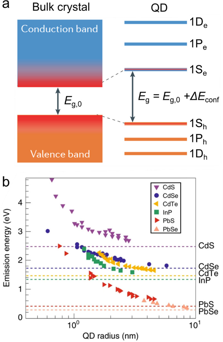
(a) A bulk semiconductor has continuous conduction and valence energy bands separated by a fixed bandgap Eg,0. A semiconductor QD features discrete atomic-like states whose energies are dependent on QD radius, R, due to the quantum-size effect. The three lowest energy levels of a spherical QD are usually labeled as 1S, 1P, and 1D. They correspond to states with the orbital momentum of the envelope wave function L = 0, 1, and 2, respectively. The QD bandgap is defined by the energy separation between the 1S electron and hole states and is given by the sum of the bulk bandgap and the confinement energy (ΔEconf), which scales approximately as 1/R2. Adapted with permission from ref (32). Copyright 2021 Springer Nature Limited. (b) Size-dependent emission energies of QDs of IV-VI (PbS,72−74 PbSe75), III-V (InP76,77), and II-VI (CdE, E = Te,78,79 Se,42,80 S78,81) semiconductors (colored symbols). The respective bulk-semiconductor bandgaps are shown by color-matched horizontal lines. Reproduced with permission from ref (15). Copyright 2021 Springer Nature Limited.
In the case of a spherical particle, the envelop wave function can be classified using two quantum numbers, L and n. L is defined by the orbital momentum of the envelope wave function, and n is the state number in a series of states with the same L. L is usually denoted using an atomic-orbital-like convention, that is, S, P, D, F, ... for states with L = 0, 1, 2, 3, ..., respectively; and n is a digit that varies from 1 to infinity. The QD states are usually denoted as “nL”. For example, states with L = 0 can be labeled as 1S, 2S, 3S, ....
In the case of an infinitely high potential barrier, the size-dependent energies of QD electron (e) and hole (h) states can be found from
| 1 |
where R is the QD radius, me and mh are the effective electron and hole masses, ℏ is the reduced Planck’s constant, and ϕn,L is the nth root of the spherical Bessel function of the Lth order. For the 1S band-edge state (L = 0 and n = 1), ϕ1S = π. The next energy state (1P) corresponds to ϕ1P = 4.49. Other states in the order of increasing energy are 1D (ϕ1D = 5.76), 2S (ϕ2S = 2π), 1F (ϕ1F = 6.99), etc. (Figure 1a). Each quantized level is (2L + 1) degenerate due to different projections of the orbital momentum described by quantum number M. This number varies from −L to +L in increments of 1. In the absence of magnetic field, it does not influence electronic-state energies.
The nanocrystal bandgap is defined by the energy separation between the band-edge electron and hole quantized levels. In the case of spherical QDs, is can be approximated by the sum of a bulk-semiconductor bandgap (Eg,0) and the energies of the 1S electron (1Se) and hole (1Sh) states (Figure 1a):
| 2 |
where meh = memh/(me + mh). This expression indicates
that the QD bandgap increases with decreasing R following
the 1/R2 dependence. The correction to
the bulk-material bandgap arising from the quantum-size effect is
defined by the confinement energy, ΔEconf = Eg – Eg,0 =  . This quantity can reach hundreds of millielectronvolt
in sufficiently small particles, which allows for facile manipulation
of emission color by varying particle dimensions. In particular, as
illustrated in Figure 1b, using size-controlled QDs of IV-VI (PbS72−74 and PbSe75), III-V (InP76,77), and II-VI
(CdTe,78,79 CdSe,42,80 CdS,78,81 HgTe and HgSe82) semiconductors, the
emission energy can be continuously tuned from the IR to the UV spectral
range. This is of great benefit to lasing application as it would
help fill spectral gaps that are not presently accessible with existing
lasers.
While the above model describes the key features of 0D nanocrystals, it does not account for all complexities of real semiconductor materials such as the existence of multiple valence sub-bands typical of II-VI and III-V semiconductors. In particular, confinement-induced mixing between different sub-bands leads to a complex, multicomponent structure of a hole wave function.71,83,84 In this situation, the description of valence band states requires an additional quantum number, F, which is the total hole angular momentum defined by the sum of the Bloch-function and the envelope-function momenta. In the notation of hole states, the F-number is commonly indicated by a subscript, that is, shown as nLF.
In II-VI and III-V materials, the angular momentum of the valence-band Bloch function is 3/2. Hence, the total momentum of the 1S band-edge hole is also 3/2 as L = 0. Due to different projections of the total angular momentum, the hole states are (2F + 1) degenerate. Based on its F-number of 3/2, the band-edge hole state (1S3/2) is 4-fold degenerate. In nanocrystals, this degeneracy is usually lifted due to effects of crystal field and shape asymmetry.85 Further splitting occurs due to electron–hole exchange interactions.85,86 All together, these effects lead to a complex “fine structure” of QD electron–hole (exciton) states that has a profound effect on QD light-emission properties and, in particular, the dependence of radiative lifetimes on temperature and applied magnetic field.85−87
2.2. Optical Gain in Nanocrystals
2.2.1. Optical Gain Mechanism
Light amplification or optical gain occurs due to the effect of stimulated emission. This process represents a response of a material to incident light. In particular, if an external stimulus (optical, electrical, or chemical) promotes the material to an excited state, instead of absorbing an incident photon it can generate a duplicate photon, which would lead to light amplification. For this effect to occur, stimulated emission must overwhelm optical absorption, which is realized under the condition of so-called “population inversion”, the situation when the number of excited species in the medium (atoms or molecules) is greater than the number of species remaining in the ground state.
To understand key features of light amplification in a QD medium, we will focus on a band-edge transition that couples the 1Se and 1Sh states (Figure 1a). These states form a two-level system that consists of 2-fold spin-degenerate valence band (VB) and conduction band (CB) levels (Figure 2a). In the unexcited QD, the VB level contains two electrons each of which can absorb an incident photon. If one of the VB electrons is promoted to the CB, this creates a single electron–hole (e-h) pair or a single-exciton state. In this case, the incident photon can be either absorbed by the electron remaining in the VB or duplicated by stimulated emission by the CB electron. These two processes compensate each other, implying that the net effect is optical transparency. If both VB electrons are promoted to the CB, this creates a two-exciton or a biexciton state. This state responds to the incident photon by stimulated emission arising from one of the other CB electron. Based on these considerations, light amplification requires biexcitons. Further, in order for stimulated emission to overwhelm absorption and thus generate net optical gain, the number of QDs excited with the biexcitons must be greater than that remaining in the ground state.
Figure 2.
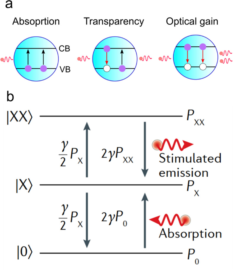
(a) A simplified optical-gain model in which a QD band-edge transition is approximated by a two-level system comprising 2-fold-degenerate VB and CB states. In its ground state, the QD can only absorb an incident photon. The single-e-h pair (single-exciton) state corresponds to optical transparency as the processes of absorption and stimulated emission compensate each other. The two-e-h-pair (biexciton) state responds to the incident photon by producing a duplicate photon via simulated emission. This leads to light amplification. (b) A three-state model used to analyze QD optical gain takes into consideration optical transitions between the QD ground (|0⟩), single-exciton (|X⟩), and biexciton (|XX⟩) states. These states occur in the QD ensemble with probabilities P0, PX, and PXX, respectively. They interact with a resonant optical field via processes of absorption (upward arrows) and stimulated emission (downward arrows) whose rates are indicated next to the arrows. The transition rates are computed for the unity photon density and are presented in terms of the rate of a single spin-allowed transition (γ).88 Because in the QD ground state, the VB level contains two electrons, the rate of the “absorbing” |0⟩ → |X⟩ transition is 2γ. A single-exciton state comprises 4 configurations with different combinations of electron and hole spins. Due to optical selection rules, only 2 of these configurations are optically active. Hence, the rates of the “emitting” (|X⟩ → |0⟩) and the “absorbing” (|X⟩ → |XX⟩) transitions originating from the single exciton are given by γ/2. In the case of the |XX⟩ state, either of the CB electrons can emit a photon via a spin-allowed transition. Hence, the total transition rate is 2γ. Adapted with permission from ref (88). Copyright 2015 American Chemical Society.
2.2.2. Optical Gain Threshold
To quantify the optical gain conditions, we will use a “three-state model” originally introduced in ref (88). This model assumes that a QD can be either unoccupied or occupied with one or two excitons (Figure 2b). The probabilities of these states are, respectively, P0, PX, and PXX, and their sum is 1. For optical gain to occur, PXX must be greater than P0, while the gain threshold corresponds to condition P0 = PXX. Given that P0 + PX + PXX = 1, this condition can be satisfied if PX = 1, that is all QDs in the gain medium are occupied with a single exciton or the average per-dot excitonic occupancy ⟨N⟩ is 1.
In a real-life experiment, when QDs are excited with short optical pulses and the pump-photon energy is well above the band-edge, the exciton distribution in a QD medium can be described by Poisson statistics for which pi = (⟨N⟩i/i!)e–⟨N⟩.89 Here pi is the probability of a QD to be excited with i excitons where i varies from 0 to infinity. In order to adapt Poisson statistics for the case of our three-state model, we assume that all multiexcitons contribute to optical gain as biexcitons, that is, PXX = 1 – p0 – p1.88 Thus, condition P0 = PXX can be rewritten as 1 – e–⟨N⟩ (1 + ⟨N⟩) = e–⟨N⟩, which yields the optical gain thresholds, ⟨Nth, gain⟩, of ∼1.15. This quantity is just slightly above ⟨Nth, gain⟩ = 1, realized for a uniform distribution of excitons in the QD ensemble.
2.3. Auger Recombination and Its Implications for Lasing
2.3.1. General Trends in Auger Recombination
The above analysis indicates that optical gain species in QDs are biexcitons and other multiexcitons of higher multiplicity. This suggests that optical gain decay is controlled not by single-exciton recombination but by multiexciton dynamics. This represents a serious complication for realizing lasing and optical gain as multiexciton recombination in 0D nanocrystals is extremely fast due to nonradiative Auger recombination.54,90−93 In this process, an e-h pair recombines not by emitting a photon but by transferring its energy to a charge carrier colocated in the same dot (Figure 3, bottom). Auger recombination directly competes with stimulated emission (Figure 3, top) and as a result it hampers the development of laser action.
Figure 3.
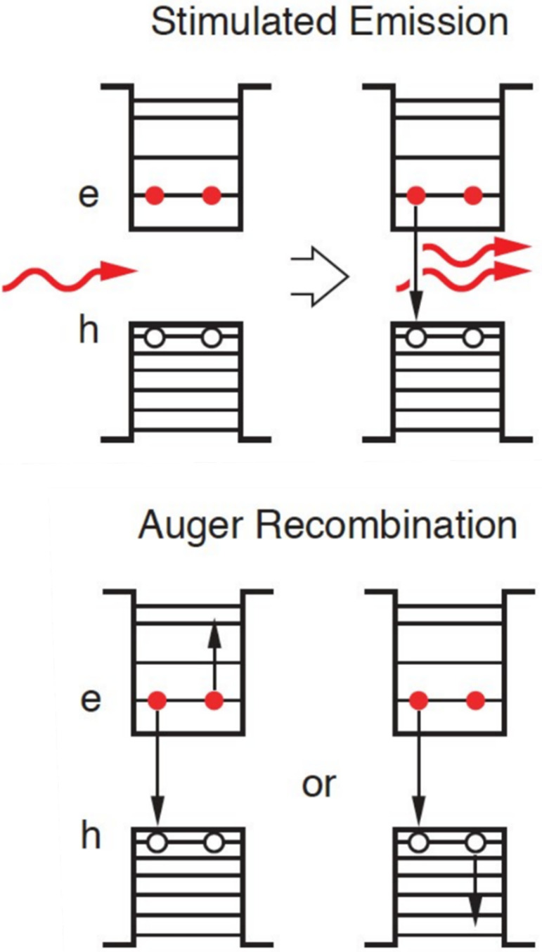
Top: Illustration of light amplification by a QD biexciton state. An incident photon triggers stimulated emission by one of the CB electrons which produces a photon duplicate. Bottom: In QDs, this process directly competes with fast biexciton nonradiative decay via the Auger process. During Auger decay, the electron–hole recombination energy dissipates by energy transfer either to an electron or a hole located in the same QD. These two recombination channels are often referred to as negative- and positive-trion pathways, respectively. Reproduced with permission from ref (32). Copyright 2021 Springer Nature Limited.
The time scales of Auger recombination and the detrimental implications of this effect for QD lasing were first analyzed in two related papers that appeared in 2000 (refs (29 and 54)). These studies focused on a series of size-controlled colloidal CdSe QD samples. They revealed quantized steps in Auger dynamics associated with decay of discreate two-, three-, and four-exciton states. This work also uncovered the “volume scaling” (known also as “V-scaling”) of Auger lifetimes, that is, direct proportionality of Auger time constants (τA) and the nanocrystal volume (VNC).54 As was demonstrated by multiple follow-up studies, this trend is remarkably general and is observed for practically all studied nanocrystal compositions including direct (e.g., CdSe, PbSe, PbS, and InASs), indirect (e.g., Ge and Si) semiconductors, as well as perovskite nanocrystals (Figure 4).39,55,89,93−100
Figure 4.
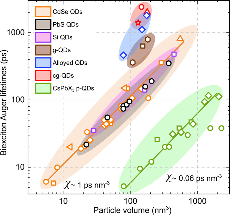
Volume scaling (V-scaling) of biexciton Auger lifetimes illustrated using series of size-controlled QDs of wide-gap II-VI CdSe (orange, brown, blue and red symbols), narrow-gap IV-VI PbS (black symbols), indirect-gap group-IV Si (purple symbols), and CsPbBr3 and CsPbI3 perovskites (green symbols). Symbols are experimental data for CdSe QDs (orange squares,89 orange circles,94 orange upright triangles,95 orange diamonds,96 and orange sidewise triangles97), PbS QDs (black circles39), Si QDs (purple squares39), CsPbBr3 perovskite QDs (green circles99 and squares100), CsPbI3 perovskite QDs (green diamonds99), thick-shell CdSe/CdS “giant” QDs (g-QDs, brown hexagons55 and square60), alloyed CdSe/CdSe0.5S0.5/CdS QDs (blue diamonds55), and continuously graded cg-QDs CdSe/CdxZn1–xSe/ZnSe0.5S0.5 (red circle,59 star,101 and triangle62). Lines are fits using V-scaling with χ = 1 ps nm–3 (orange line; CdSe, PbS, and Si QDs) and χ = 0.06 ps nm–3 (greenline; perovskite QDs). Adapted with permission from ref (32). Copyright 2021 Springer Nature Limited.
Importantly, nanocrystals of different materials exhibit not only the same functional (linear) dependence of τA on VNC but nearly the same time constants for a given nanocrystal volume. The effect of “convergence” of Auger time constants is especially dramatic if one compares nanocrystals of direct (e.g., CdSe) and indirect (e.g., Ge) semiconductors.93 In the bulk form of these materials, Auger lifetimes differ by orders of magnitude. This is due to the difference in the recombination mechanism which requires participation of phonons in indirect materials and is phonon-less in direct semiconductors. However, this distinction disappears in the case of the nanocrystals that show very similar time constants for particles of the same volume.93
In the case of biexcitons, V-scaling can be presented as τA,XX = χV, where χ is a “universal” constant of ∼1 ps nm–3, which is independent of nanocrystal composition39,54,93 (Figure 4, orange line). So far, the only investigated system for which the value of χ is different is perovskite nanocrystals. Their Auger lifetimes also follow V-scaling; however, the χ constant is considerably smaller than for, for example, II-VI and IV-VI semiconductors. In particular, based on the measurements of CsPbBr3 and CsPbI3 perovskite nanocrystals, χ is approximately 0.06 ps nm–3 (Figure 4, green line), implying that the Auger lifetimes in this case are more than an order of magnitude shorter than for moretraditional semiconductor compositions.
Based on conventional V-scaling with χ = 1 ps nm–3, the biexciton Auger lifetime varies from ∼4 ps to ∼270 ps for spherical QDs with radii from 1 to 4 nm, which is the size range of typical CdSe nanocrystals. These time constants are much shorter than biexciton radiative lifetimes (τr,XX) that are on the nanosecond time scale.32,102 This implies that even in the absence of defect-related nonradiative channels, biexciton emission efficiencies are extremely low (typically, 0.1 to 5%, depending on nanocrystal size32) due to intrinsic Auger decay. Apparently, this creates a serious problem in the case of lasing applications as optical gain in nanocrystals relies on stimulated emission from biexcitons.
2.3.2. Implications for Lasing: Critical Nanocrystal Concentration
Fast multiexciton Auger recombination leads to very short optical gain lifetimes. As was first realized in ref (29), this can prevent light amplification unless the nanocrystal concentration is sufficiently high for stimulated emission to outpace Auger decay. The nanocrystal concentration (ρ) needed to meet this requirement is defined by the condition that the rate of stimulated emission under gain saturation (rSE,0) is greater than the rate of biexciton Auger decay (rA,XX = 1/τA,XX). The critical concentration (ρ = ρcrit) corresponds to the situation then the two rates are equal to each other, that is, rSE,0 = 1/τA,XX. Quantity rSE,0 can be expressed as rSE,0 = β(c/nr)G0, where G0 is the saturated gain coefficient (realized when all nanocrystals in the medium contain two or more excitons), c is the speed of light, nr is the refractive index, and β is a dimensionless constant dependent on details of a coupled QD-cavity system.29,88 If we express G0 as G0 = ρσgain,XX (σgain, XX is the biexciton gain cross-section), we obtain ρcrit = nr (βcσgain,XXτA,XX)−1.
It is convenient to present the critical condition in terms of a volume fraction of a semiconductor material in the nanocrystal sample (ξ). For this purpose, we use relationship ξ = ρVNC, which yields
| 3 |
This expression indicates that the critical semiconductor volume fraction required for laser action increases with decreasing Auger lifetime following the 1/τA,XX dependence. Using eq 3 and Auger time constants typical of standard (nonengineered) nanocrystals, we obtain that ξcrit is from ∼0.2% to ∼2%, depending on nanocrystal size.29,88 Such volume fractions can be easily realized with close-packed QD films for which ξ is normally greater that 10%. These considerations motivated the use of dense, solid-state QD samples in the first demonstration of ASE with colloidal nanocrystals.29 In addition, the study presented in ref (29) used femtosecond optical pump pulses whose duration (τp = 100 fs) was much shorter than the biexciton Auger lifetime. This allowed for minimizing Auger-related carrier losses during the stage of the preparation of the optical-gain state. Following this original publication, the majority of optical gain and lasing studies of colloidal nanocrystals have utilized the same approach, that is, the combination of solid-state films as an optical gain medium and a short-pulse laser as a pump source.
2.3.3. Effect of Auger Decay on Gain and Lasing Thresholds
In the case of short-pulse excitation when τp ≪ τA,XX, the per-pulse fluence (wp) required to achieve the gain threshold is given by wth,gain = hνp⟨Nth,gain⟩/σabs, where hνp is the pump photon energy and σabs is the corresponding nanocrystal absorption cross-section. In the case of Poisson statistics of photon absorption events (Section 2.2.2), this yields wth,gain = 1.15hνp/σabs. This quantity does not depend on the Auger lifetime, indicating that in the case of short-pulse pumping, Auger decay has no influence on optical gain thresholds.
The situation changes in the case of cw excitation. To analyze the cw regime, we will use the three-level system discussed previously in Section 2.2.2 and displayed in Figure 2b. In the prelasing regime, when the role of stimulated emission is weak, biexciton decay (time constant τXX) occurs via spontaneous radiative decay and Auger recombination, which yields the overall time constant expressed as τXX = τA,XXτr,XX /(τA,XX + τr,XX). Under steady state conditions, biexciton decay is compensated by pump-induced exciton-to-biexciton transitions, that is, PXX/τXX = gexcPX, where gexc is the excitation rate. Similar considerations applied to the ground and single-exciton states yield PX/τX = gexcP0. Combing the two expressions together, we obtain PXX = gexc2τXXτXP0. Further, using the gain-threshold condition (PXX = P0), we find that the cw excitation rate required to attain the gain threshold is given by gexc,th,gain = (τXXτX)−1/2. If expressed in terms of the excitation intensity (I = gexchνp/σabs), the gain threshold is Ith,gain = (hνp/σabs)(τXXτX)−1/2.
The above expressions indicate direct dependence of gain threshold on the biexciton lifetime. In the case of ordinary (nonengineered) nanocrystals, the biexciton decay is dominated by Auger recombination, that is, τXX ≈ τA,XX. As τA,XX decreases with particle size, the realization of steady-state optical gain regime becomes progressively more difficult as nanocrystal dimensions are reduced. For example, for spherical QDs, τA,XX follows the R–3 dependence, which leads to the R–3/2 dependence for Ith,gain.
Even more significant are the implications of fast Auger decay for lasing thresholds, as the realization of the lasing regime requires that a substantial number of nanocrystals are excited with gain-active biexcitons in order to both compete with Auger decay and compensate optical losses due to light scattering and absorption in a complex device structure. To estimate the lasing threshold, we will assume that the realization of laser action requires half-saturated optical gain, that is, the gain coefficient (G1/2) which is equal to 0.5G0. Within the three-state model, the optical gain coefficient can be expressed as G = G0 (PXX – P0). Hence, condition G = G1/2 = 0.5G0 can be satisfied if 2(PXX – P0) = 1. Combining this relationship with the expressions for gexc-dependent probabilities PXX and PX obtained earlier and taking into consideration the normalization condition (P0 + PX + PXX = 1), we obtain that the excitation rate required to achieve G1/2 is
| 4 |
or gexc,1/2 ≈ 1/τA, XX, if we assume that τXX is dominated by Auger decay. If presented in terms of the excitation intensity (I1/2), meeting the G1/2 condition requires pump intensity I1/2 = hνp/(σabsτA,XX).
The above considerations
indicate that Auger recombination has
a stronger effect on the lasing threshold than the optical gain threshold.
The ratio of the two quantities can be estimated from I1/2/Ith,gain ≈ . This expression suggests that the realization
of lasing becomes progressively more difficult than the realization
of optical gain as the nanocrystal size is reduced as this leads to
shortening of the Auger lifetime.
To illustrate the difference between I1/2 and Ith,gain, we consider midsize nanocrystals with R = 2.5 nm. Based on V-scaling, their biexciton Auger lifetime is ∼65 ps. If single-exciton decay is due primarily to radiative recombination (that is, τX ≈ τr,X), its room-temperature time constant is size independent and in the case of CdSe QDs is ∼20 ns.103 These parameters yield I1/2/Ith,gain of approximately 20.
It is also illustrative to estimate the magnitude of I1/2. In our estimations, we assume that the CdSe QD sample with R = 2.5 nm is excited at 3 eV. The corresponding absorption cross-section is ca. 3 × 10–15 cm2.39 Using these parameters along with our earlier estimation of τA,XX, we obtain I1/2 = 2.5 MW cm–2. This extremely high intensity cannot be withstood by colloidal nanocrystals without damage, which explains the difficulty for achieving cw lasing with these materials and highlights the need for effective approaches for suppression of Auger recombination. Specifically, in order to reduce I1/2 to a few tens of kW cm–2 or less (that is, to levels compatible with colloidal nanostructures), it is necessary to increase the product of τA,XX and σabs by a factor of least 100. In the next Section, we discuss approaches for accomplishing this objective.
2.4. Control of Auger Recombination
2.4.1. “Giant” Core/Shell QDs and the Realization of cw Lasing
One approach to lower lasing thresholds entails the use of core/shell hetero-QDs that contain a small “emitting” core encased within a thick shell of a wider-gap semiconductor. On the one hand, this increases the QD absorption cross-section as the shell serves as a light-harvesting antenna. On the other hand, this can lengthen the Auger lifetime if the carrier wave functions leak into the shell region and thereby increase their localization volume.
In ref (60), this strategy was implemented with so-called “giant” QDs (g-QDs) wherein a CdSe core was enclosed into a thick CdS shell. In these structures, the hole is tightly confined to the core due to a large VB barrier. Because of a much lower CB barrier, the electron wave function extends into the shell due to which the biexciton Auger lifetime lengthens to 600 ps. Simultaneously, the presence of a thick shell leads to the increased absorption cross-section which reaches 5.5 × 10⁻¹⁴ cm2 at 2.8 eV used in the lasing experiments. Using the expression for I1/2 derived in the previous section, we estimate that the realized enhancements in τA,XX and σabs should lower I1/2 to about 14 kW cm–2, the level thatcould be withstood by the nanocrystals. Indeed, the use of these core/shell QDs allowed for demonstrating cw lasing using devices wherein the CdSe/CdS QDs were combined with a 2D photonic crystal cavity. In good agreement with the above estimations, the observed lasing thresholds were 6.4–8.4 kW cm–2.
While providing proof of feasibility of cw lasers based on colloidal nanocrystals, the studies in ref (60) also indicated the need for a more complete suppression of Auger recombination in order to further lower lasing thresholds. At pump powers used in that work, the lasing regime was sustained only for 10 to 30 min at which point devices failed due to excessive overheating.
2.4.2. Compositionally Graded QDs
It has been demonstrated that Auger decay can be also suppressed by grading the composition of the QD interior.55−59 The introduction of compositional gradients smoothens carrier confinement potential and thereby impedes Auger recombination by reducing the rate of intraband transitions involved in the dissipation of the electron–hole recombination energy.104,105
Originally, the grading strategy was implemented by inserting a thin alloyed CdSexS1–x interlayer between a CdSe core and a thick CdS shell (Figure 5a,b).55,56 This approach proved to be very effective. In particular, the biexciton lifetime increased to 1.6 ns from 350 ps for standard “giant” CdSe/CdS QDs.55 The extended τA,XX had a positive impact on the biexciton emission quantum yield (qXX), which was boosted to 11% from ∼3% in QDs without an alloyed interlayer.55 An increasingly smoother potential profile, obtained by increasing the number of alloying steps, led to even stronger suppression of Auger decay.57 This was reflected in the increasing qXX, which reached ∼30% in the structures with 5 alloying steps (Figure 5c,d).
Figure 5.
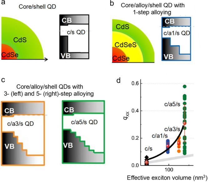
(a) A schematic depiction of a core/shell CdSe/CdS QD (left) and its band diagram (right). (b) Same for a CdSe/CdSexS1–x/CdS QD with an alloyed CdSexS1–x interlayer (1-step alloying). (c) A core/alloy/shell CdSe/CdSexS1–x/CdS QD (left) wherein an alloyed interlayer comprises 3 (left) and 5 (right) layers with different Se-to-S ratios, which leads to a progressively more gradual change of the confinement potential. (d) The increase in the number of alloying steps leads to the increased biexciton emission quantum yield (qXX) indicating more complete suppression of Auger decay. The black, blue, orange, and green symbols are data points obtained using single-dot measurements. The black line is a guide for the eye which describes the dependence of the average biexciton emission quantum yields (red symbols) on effective exciton volume. The gray line is the trend expected for traditional V-scaling of Auger lifetimes. Considerable deviation between the black and the gray lines which increases with the number of alloying steps indicates the increasing degree of Auger-decay suppression. Adapted with permission from ref (57). Copyright 2014 American Chemical Society.
The most recent advance in the area of Auger-decay engineering has been the development of continuously graded QDs (cg-QDs) implemented with a CdSe/CdxZn1–xSe system (Figure 6a).59,61,106 In contrast to quasi-type-II CdSe/CdS QDs, wherein interfacial alloying affects primary the hole confinement potential (Figure 5), the use of type-I CdS/CdxZn1–xSe QDs allows one to realize a gradually varying potential for both the electron and the hole (Figure 6b). This helps achieve a stronger suppression of Auger recombination by impeding Auger-decay channels involving re-excitation of both an electron and a hole (Figure 3, bottom).
Figure 6.
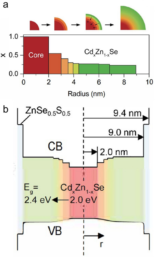
(a) A compositional profile along the radial direction in a cg-QD that comprises the 2 nm-radius CdSe core followed by the 7 nm compositionally graded CdxZn1–xSe shell. (b) The corresponding profiles of the CB and VB confinement potentials. Reproduced with permission from ref (59). Copyright 2017 Nature Publishing Group.
In Figure 6, we display an example of a thick-shell compositionally graded CdSe/CdxZn1–xSe/ZnSe0.5S0.5 cg-QD that contains a 2 nm CdSe core radius, a 7 nm graded CdxZn1–xSe shell, and a final 0.4 nm ZnSe0.5S0.5 protective layer. An important structural feature of the cg-QDs is a strong asymmetric compression of the CdSe core that develops as a result of anisotropic lattice mismatch at the CdSe/CdxZn1–xSe interface.106 This leads to pronounced modifications in their properties including the increase of the light–heavy hole splitting (Δlh) to more than 40 meV and shortening of the single-exciton radiative lifetime, which becomes ∼12 ns versus ∼20 ns in core-only CdSe QDs.106 These properties are beneficial for lasing, as a large Δlh increases the relative occupancy of the band-edge heavy-hole state, which lowers the gain threshold.60 The shortened τr,X implies an increased emission dipole, which translates into the increased gain cross-section.
Other beneficial features of cg-QDs are a large absorption cross-section (1.8 × 10⁻¹³ cm2 at 3.1 eV) and a long biexciton Auger lifetime (τXX ≈ 1.3 ns). Using the latter value and a biexciton radiative lifetime of 3 ns (τr,XX = τr,X/4; ref (102)), we obtain that the biexciton Auger lifetime is as long as 2.3 ns. This is comparable to the biexciton radiative lifetime, indicating very strong Auger-decay suppression. In fact, based on the time constants of cg-QDs, their biexciton emission quantum yield reaches 43%, a striking difference from standard CdSe QDs wherein biexcitons are virtually nonemissive.
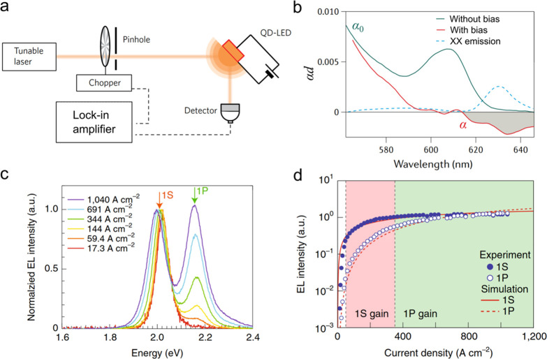
The discovery of cg-QDs accelerated the progress toward technologically viable laser devices including electrically pumped laser diodes. One significant development was the demonstration of low-threshold distributed feedback (DFB) lasers operating in the subsingle-exciton regime.61 These devices took advantage of strong suppression of Auger recombination for negatively charged excitons that were used as gain-active species. Further, the cg-QDs were applied to realize for the first time electrically excited optical gain in LEDs with a special “current focusing” charge-injection architecture.59 A related development was the demonstration of devices that operated at ultrahigh current densities of ∼1000 A cm–2 that allowed for achieving optical gain at both the band-edge (1S) and the high-energy (1P) transitions.16 The cg-QDs were also employed in dual-function devices that were based on a high-current-density LED supplemented by an integrated DFB cavity.17 These devices operated as an electroluminescent (EL) structure under electrical bias and as a DFB laser under optical pumping. The most recent breakthrough enabled by the cg-QDs was the demonstration of prototype laser diodes that produced intense edge-emitted ASE under electrical excitation.63 Some of the above advances are overviewed in greater details in Section 6 of this review.
3. Practical Aspects of Optical Gain and Advanced Gain Concepts
3.1. Optical Gain Characteristics
3.1.1. Definitions
When light propagates in an optical gain medium, photons are multiplied by the process of stimulated emission, which leads to light amplification. For a given amplification length (l), the output light intensity (Iout) can be related to the input intensity (Iin) and the gain coefficient (G) by Iout = IineGl. As we indicated earlier, G can be related to the gain cross-section (σgain) and the nanocrystal concentration (ρ) by G = ρσgain.
We define material gain (Gmat) as the gain coefficient of an infinitely thick close-packed QD film. Another quantity used in the literature is a “bulk-equivalent” gain coefficient (GB).107,108 It can be related to Gmat using the semiconductor volume fraction in a sample by GB = ξ–1Gmat. This gain coefficient corresponds to the ideal situation when nanocrystals are packed so as ξ = 1.
An important device characteristic is the modal gain coefficient which can be expressed as Gmod = ΓNCGmat. Here ΓNC is a “mode-confinement” factor that is defined by the degree of optical-mode confinement within the gain medium. It is computed as the ratio of the energy of the optical mode residing within the nanocrystal optical gain layer and the total mode energy. Typically, in nanocrystal films with thickness ∼300 nm or more, ΓNC is close to 1. Therefore, the measurements of such thick films yield gain values that are close to Gmat. In EL devices that employ thin nanocrystal films, ΓNC can be considerably smaller than 1, which diminishes overall gain generated in the device. In well-designed optical-gain EL devices, ΓNC can reach values of 0.3–0.4.62
Another useful device-related characteristic is net optical gain (Gnet). This quantity is defined as the difference between the modal gain coefficient generated in the active medium and the loss coefficient (αloss) associated with light absorption and scattering in various components of a complex device structure. Based on this definition, Gnet = Gmod – αloss.
Earlier, we also introduced the term “saturated” gain. Gain saturation corresponds to the situation of the maximal gain coefficient achievable for a given optical transition. In a simple model of 2-fold-degenerate band-edge states (Figure 2), gain saturation is achieved when all nanocrystals in the sample are excited with biexcitons or other multiexcitons of higher order. To indicate that a certain gain characteristic corresponds to gain saturation, we will use the subscript “0” (e.g., G0,mat or G0,mod).
3.1.2. Transient Absorption Measurements of Optical Gain
Optical gain characteristics of nanocrystal materials are often evaluated using a transient absorption (TA) pump–probe spectroscopy. In the TA experiment, a sample (prepared as a solution or a solid-state film) is excited above a bandgap by a short “pump” pulse that generates nonequilibrium e-h pairs in the nanocrystals. The presence of photoinjected carriers modifies the absorption coefficient of the nanocrystal sample (α) due to effects such as state-filling and Coulomb carrier–carrier interactions.89,109 The corresponding absorption change (Δα = α – α0; here α0 is the ground-state absorption coefficient of an unexcited sample) evolves in time, which reflects the carrier relaxation and recombination dynamics. This evolution is probed by a variably delayed narrow-band or broadband (supercontinuum) “probe” pulse (Figure 7a).
Figure 7.
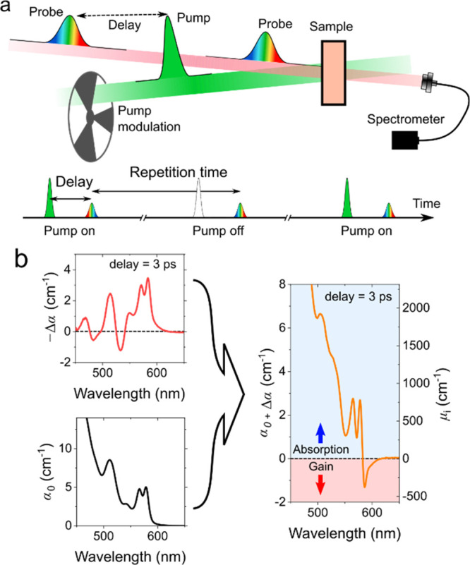
(a) Top: a scheme of a transient absorption (TA) pump–probe experiment wherein an absorption change (Δα) induced by a pump pulse is probed with a time-delayed probe pulse. Bottom: a time-synchronized pulse sequence in which every second probe pulse arrives together with the pump pulse. The probe signals recorded with and without pump pulses yield absorption coefficients of the excited (α) and unexcited (α0) sample, respectively. As a result, this scheme allows one to obtain the pump-induced absorption change (Δα = α – α0) for each pair of adjacent pump pulses and then average it across the entire pulse sequence. (b) An illustration of how the acquired spectrum of Δα (top left) is summed with the ground-state-absorption spectrum (α0; bottom left) to obtain the excited state absorption spectrum (α = α0 + Δα; right). Optical gain manifests in excited-state absorption as negative absorption features with α < 0.
In TA experiments, a signature of optical gain is photoinduced bleaching (Δα < 0) whose magnitude is greater than α0(|Δα| > α0). In this situation, the absorption of a photoexcited sample becomes negative, that is, α = α0 – |Δα| < 0 (Figure 7b). Usually, this situation is realized for certain spectra bands (Figure 7b, right), which will be referred to as optical-gain bands.
By analyzing α as a function of pump intensity (evaluated, e.g., as the average nanocrystal excitonic occupancy, ⟨N⟩) one can obtain the gain threshold ⟨Nth,gain⟩ from the intensity at which α becomes zero. Further, based on the magnitude of α observed past the threshold, one can derive the gain coefficient (G = |α|) and, then, use it to compute other characteristics of interest such as the gain cross-section, the bulk-equivalent gain coefficient, etc.
3.1.3. Variable Stripe Length Measurements of Optical Gain
The optical gain of solid-state films that show ASE is commonly measured using a variable stripe length (VSL) technique.110 In this method, the sample is excited using a laser beam focused with a cylindrical lens onto a sample. Using this approach, the excited spot is shaped as a narrow stripe that ends at (or crosses) one of the sample edges (Figure 8a). The edge-emitted light intensity is measured as a function of stripe length (l). If the pump level is above the gain threshold and the nanocrystal density exceeds the critical value (ρ > ρcrit; Section 2.3.2), the sample will exhibit ASE when l becomes sufficiently long. In spectrally resolved measurements, this manifests as the emergence of sharp features which spectrally match the optical-gain bands (Figure 8b). This effect, commonly referred to as “line narrowing”, is one of the attributes of the ASE regime. Line narrowing is accompanied by the fast exponential growth of the emitted intensity IPL (symbols in Figure 8c), which can be described by IPL = Al + BeGl (line in Figure 8c). Here the first (linear) term arises from spontaneous emission and the second (exponential) term is the contribution from ASE (parameters A and B are length-independent constants). By fitting the measured l-dependent intensity to the above expression, one can derive the gain coefficient. As was indicated earlier, in the case of sufficiently thick, low-loss films, this procedure yields the material gain coefficient. The VSL technique is also very useful in the case of devices where it allows one to evaluate net optical gain.62
Figure 8.
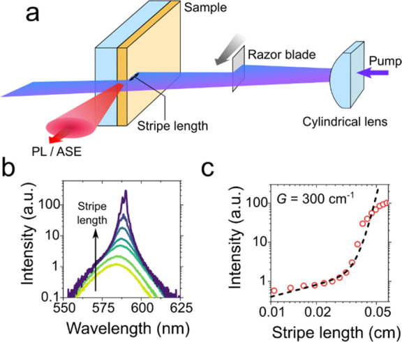
(a) Optical gain measurements using a variable stripe-length (VSL) technique. In this method, a nanocrystal film is excited with a laser beam focused with a cylindrical lens into a narrow stripe, aligned perpendicular to the sample edge. The edge emitted light intensity is measured as a function of stripe length varied with a razor blade translated in or out of the laser beam. (b) An example of VSL measurements, which exhibit the emergence of a narrow ASE feature at sufficiently large stripe lengths (l). (c) The measured edge-emitted emission intensity (IPL; circles) is fitted to IPL = Al + BeGl (line), where G is the gain coefficient, and A and B are l-independent constants.
3.2. Advanced Optical Gain Concepts
3.2.1. Single-Exciton Gain due to “Giant” Exciton–Exciton Repulsion
As discussed earlier, band-edge optical gain arises from biexcitons and other multiexcitons of higher order. The resulting complication is very fast gain relaxation due to nonradiative Auger recombination. This greatly complicates the realization of lasing with cw optical excitation (Section 2.4.1), and as will be discussed in Section 5, represents a significant impediment in the case of electrical pumping.
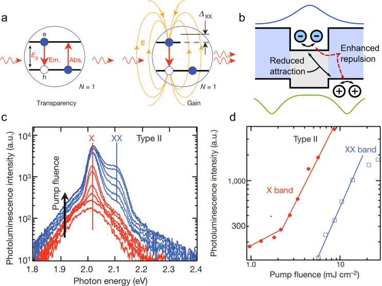
As was first proposed in ref (111), one approach to resolve the problem of fast optical gain relaxation is to create conditions under which gain becomes possible with single excitons, the species that are not subject to Auger decay. To implement this idea, it was proposed to use strong exciton–exciton repulsion to upshift the “absorbing” transition of a singly excited nanocrystal so it does not compete with the “emitting” single-exciton transition (Figure 9a). As discussed earlier, in the absence of exciton–exciton interactions, the “absorbing” upward transition in a QD occupied with a single exciton (|X⟩ → |XX⟩ in Figure 2b) has the same energy and strength as the downward emitting transition (|X⟩ → |0⟩ in Figure 2b). As a result, the two transitions compensate each other implying that a single-exciton state is “optically transparent”, that is, it does not absorb nor amplify incident photons.
Figure 9.
(a) The illustration of a concept of single-exciton optical gain in QDs that feature strong exciton–exciton repulsion. In the absence of exciton–exciton Coulomb interactions, the single exciton state corresponds to optical transparency as the probability of photon absorption is equal to the probability of stimulated emission and both the “absorbing” and the “emitting” transitions have the same energy (left). In the presence of exciton–exciton repulsion, the “absorbing” transition in a QD containing an exciton is shifted up in energy. This shift is defined by the energy of exciton–exciton interaction (ΔXX). If ΔXX is greater than the QD ensemble line width, stimulated emission occurs without interference from the absorbing transition which leads to “single-exciton gain”. Adapted with permission from ref (112). Copyright 2007 Nature Publishing Group. (b) The repulsive exciton–exciton interaction can be realized using type-II heterostructures wherein electrons and holes are separated between different parts of the QD (e.g., the core and the shell, as shown in the picture). The blue and green curves depict electron and holes wave functions, respectively. Adapted with permission from ref (115). Copyright 2007 American Chemical Society. (c) Pump-fluence-dependent emission from a film of type-II CdS/ZnSe QDs shows the emergence of two ASE bands. The lower-energy feature, which develops at the center of the single-exciton spontaneous PL band, is due to single-exciton gain (labeled as ‘X’; red lines). The higher-energy feature is due to the standard biexciton gain mechanism (labeled as ‘XX’; blue line). (d) The amplitudes of the X and XX emission bands measured as a function of pump fluence indicate that the threshold of the single-exciton ASE (2 mJ cm–2) is appreciably lower than the threshold of the biexciton ASE (6 mJ cm–2). Panels (c) and (d) adapted with permission from ref (112). Copyright 2007 Nature Publishing Group.
The situation, however, changes in the presence of exciton–exciton interactions. For example, if the excitons repel each other, the energy of the absorbing (|X⟩ → |XX⟩) transition becomes greater than that of the emitting (|X⟩ → |0⟩) transition by ΔXX, where ΔXX is the exciton–exciton interaction energy (Figure 9a). If ΔXX is greater than the transition line width, absorption ceases to interfere with emission and optical gain becomes possible with single excitons.112 Importantly, a similar regime can be realized with exciton–exciton attraction, which leads to a downshift of the band-edge absorbing transition.113 However, a potential deficiency of such an approach is interference from higher-energy absorption features that will also be pulled down and thus might become resonant or near-resonant with the emitting transition.
Importantly, in order for single-exciton gain to be practical, the exciton–exciton interaction energy (ΔXX) must exceed a large inhomogeneous line width of a nanocrystal ensemble sample, which is at least ∼50 meV and often more. Such large energies are greater than typical exciton–exciton interaction energies in core-only or standard type-I core/shell QDs.94,109,113 In addition, in standard nanocrystals, the exciton–exciton interaction is attractive. Therefore, the realization of strong-exciton repulsion requires specially engineered nanostructures.114,115
The concept of single-exciton gain was first practically implemented in ref (112) using type-II CdS/ZnSe core/shell QDs. In these heterostructures, the built-in energy gradient separates an electron and a hole between the core and the shell regions (Figure 9b). Similar separation occurs for the second e-h pair. As a result, two electrons are colocalized in the core, while two holes, in the shell. Such distribution of charges increases Coulombic repulsion and simultaneously decreases Coulombic attraction. The net effect is very strong exciton–exciton repulsion whose characteristic energy can reach ∼100 meV.112,114,116
The use of CdS/ZnSe allowed for demonstrating single-exciton gain as was evidenced by the ASE feature emerging at the center of the exciton spontaneous emission (Figure 9c, red traces112). At higher pump levels, the sample also exhibited the second ASE band, which was due to the standard biexciton gain mechanism (Figure 9c, blues traces). Importantly, this band was blue-shifted from the peak of excitonic emission by 100 meV, confirming strong exciton–exciton repulsion realized in these type-II nanocrystals. As expected, the ASE threshold observed for the single-exciton band was considerably lower than that for the biexciton ASE feature (Figure 9d).
More recent studies demonstrated that the sign and the magnitude of the exciton–exciton interaction energy can be tuned by changing structural parameters of CdSe/CdS QDs.117 This capability was utilized to confirm direct correlations between the sign of ΔXX and the position of the ASE band versus the peak of single-exciton emission.117
3.2.2. Charged Exciton Gain
The concept of charged-exciton gain was first proposed and realized in ref (118) in 2004. Recently, it was employed to demonstrate single-mode DFB lasers that operated at ultralow, subsingle-exciton pump levels.61 The main idea behind this approach is to use not excitons but permanent charges (dopants) to bleach the band-edge absorption and thereby reduce optical gain thresholds. In fact, when the band-edge absorption is completely suppressed, the condition of the optical gain threshold is achieved in the ground state without excitation. This situation corresponds to so-called “zero-threshold” optical gain.119
In the case of II-VI nanocrystals, this concept is usually realized using electrons as the CB edge is characterized by a lower degeneracy than the VB edge and, hence, it can be saturated with a lesser number of charges. Further, in II-VI nanocrystals, negatively charged excitons have slower Auger dynamics than positively charge states,39,57,120 which leads to a longer optical gain lifetime.
Figure 10a illustrates the distinctions between standard biexciton and charged-exciton gain mechanisms realized in neutral and negatively charged QDs, respectively.61,119 In a neutral QD, the single-exciton state contributes equally to absorption and stimulated emission, which corresponds to “optical transparency” (that is, this state does not produce either optical absorption or gain). In this case, gain occurs due to stimulated emission from biexcitons and it competes with absorption by unexcited QDs, which leads to G ∝ (PXX – P0). The gain threshold occurs then PXX = P0. As was discussed in Section 2.2.2, this condition can be satisfied if PXX = 1 or ⟨Nth,gain⟩ = 1 (Figure 10a,b; left).
Figure 10.
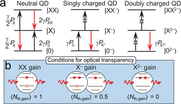
(a) Optical transitions in a neutral (left), singly charged (middle), and doubly charged (right) QD. Black and red arrows show optical transitions that correspond to, respectively, absorption and stimulated emission. P0, PX, PXX are the probabilities for the QD to be in the ground state (|0⟩), single-exciton state (|X⟩), or biexciton (|XX⟩) state. γ is the rate of a single spin-allowed transition. In the neutral QDs, single excitons do not contribute to optical gain. In this case, optical gain is the net result of the competition between stimulated emission from the biexcitons and absorption due to the unexcited QDs. In the singly charged QDs, net gain is due to the competition between stimulated emission from the charged excitons (trions) and absorption arising from the unexcited QDs. In the doubly charged QDs, ground-state absorption is eliminated, and gain is due to stimulated emission from the doubly charged excitons. (b) A schematic depiction of the optical gain-threshold condition (or the condition for “optical transparency”) in a neutral (XX, left), singly charged (X–, center) and doubly charged (X2–, right) QD. Panels (a, b) adapted with permission from ref (61). Copyright 2019, The American Association for the Advancement of Science.
For a QD with a pre-existing electron, a negatively charged exciton (trion, X–) is gain active, as the absorbing transition is blocked due to complete saturation of the band-edge CB state. In this case, the gain coefficient is proportional to (PX– – P0). Hence, gain threshold occurs when PX– = P0 = 0.5 (here, we assume that the QD ensemble contains only unexcited and singly excited dots). This corresponds to ⟨Nth,gain⟩ = 0.5 (Figure 10a, b; center). In a QD with two permanent electrons, the band-edge transition is completely bleached without excitation; therefore, ⟨Nth,gain⟩ = 0 (Figure 10a,b; right). This corresponds to “zero-threshold” optical gain.
The optical gain condition can be generalized for QDs with arbitrary
degeneracy factors of the electron (ge) and hole (gh) states and an arbitrary
number of permanent electrons residing in a dot (ne).32 In the case when a QD
ensemble is excited with ⟨N⟩ excitons,
the total average per-dot number of electrons and holes are ⟨Ne⟩ = ⟨N⟩
+ ne and ⟨Nh⟩ = ⟨N⟩, respectively.
The corresponding electron and hole quasi-Fermi potentials can be
found from  and
and  .32 Combining
these expressions with the optical gain condition (ϕe + ϕh = 0),32 we obtain that the optical gain threshold is
| 5 |
If we apply eq 5 to QDs with 2-fold-degenerate states (ge = gh = 2), this leads to ⟨Nth,gain⟩ = (ge – ne)/2. In the case, of singly charged dots with ne = 1, this expression yields ⟨Nth,gain⟩ = 0.5, the result obtained earlier based on qualitative considerations illustrated in Figure 10a,b (center).
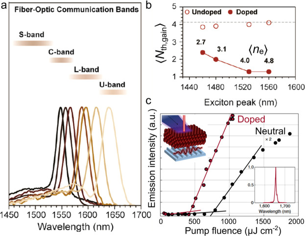
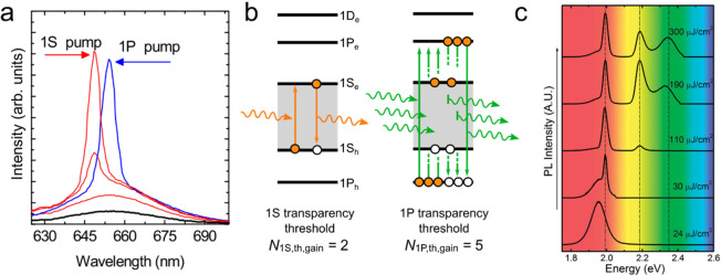
The effects of charging can be especially beneficial in the case of materials with highly degenerate CB and VB band-edge states such as PbSe and PbS QDs.121,122 The band structure of these semiconductors features four equivalent valleys at the L points of the Brillouin zone. Together with the 2-fold spin degeneracy, this leads to the 8-fold-degenerate electron and hole band-edge states (ge = gh = 8).122 In the case of neutral dots, the corresponding gain threshold is ⟨Nth,gain⟩ = 4, which is four times higher than that for QDs with 2-fold degenerate states. However, if the QD is charged with 6 permanent electrons, then, according to eq 5, the gain threshold drops to ⟨Nth,gain⟩ = 1, as in the case of dots with ge = gh = 2.
It is important to realize that while the use of charged excitons reduces the optical gain threshold, this mechanism is still affected by Auger recombination, as light amplification occurs due to multicarrier states such as trions and/or multiply charged excitons. Importantly, in this case, the influence of Auger effects is weaker than for neutral QDs. To illustrate this, we will consider PbSe(S) QDs that feature highly degenerate band-edge states. As was shown previously,97 in these QDs, Auger lifetimes can be accurately described by so-called “statistical scaling” according to which
| 6 |
where Ne and Nh are the per-dot numbers of electrons and holes, respectively, and CA is a constant. We will use this expression to compare Auger lifetimes at the gain threshold in the case of neutral and changed QDs with ne = 6. For the former case, we obtain 1/τA = 4 × 4(4 + 4–2)CA = 96CA. For the latter case, 1/τA = 7 × 1(7 + 1–2)CA = 42CA. Based on these expressions, the Auger lifetime in charged dots is 2.3 times longer than in neutral dots, despite a high level of QD charging. Importantly, this advantage is combined with a considerably lower gain threshold (⟨Ngain⟩ = 1 versus 4). As was demonstrated recently, the use of charged-exciton gain indeed simplifies realization of lasing with PbS QDs, a material which allows one to obtain spectrally tunable emission in the technologically important range of IR wavelengths.123,124
3.3. Practical Implementations of Charged-Exciton Gain and Lasing
3.3.1. Electrochemical Charging
To realize charged-nanocrystal optical gain, permanent (or long-lived) electrons have been injected using electrochemical, photochemical, and chemical techniques.118,119,123 The original demonstration of this concept and some follow-up studies employed electrochemical doping.118,125 For this purpose, QDs are deposited onto a conductive electrode (a work electrode) and immersed into an electrolyte together with reference and counter electrodes (Figure 11a). Application of a negative potential to the work electrode results in injection of electrons into the QDs. Monitoring the linear absorption of the QD sample reveals bleach of the band-edge transition whose magnitude can be used to evaluate the degree of QD charging. As illustrated in Figure 11b, using this approach, it is possible to achieve complete bleaching of the band-edge transition.126 This indicates the injection of at least two electrons per-dot on average, the condition required for the realization of “zero-threshold” optical gain.119
Figure 11.
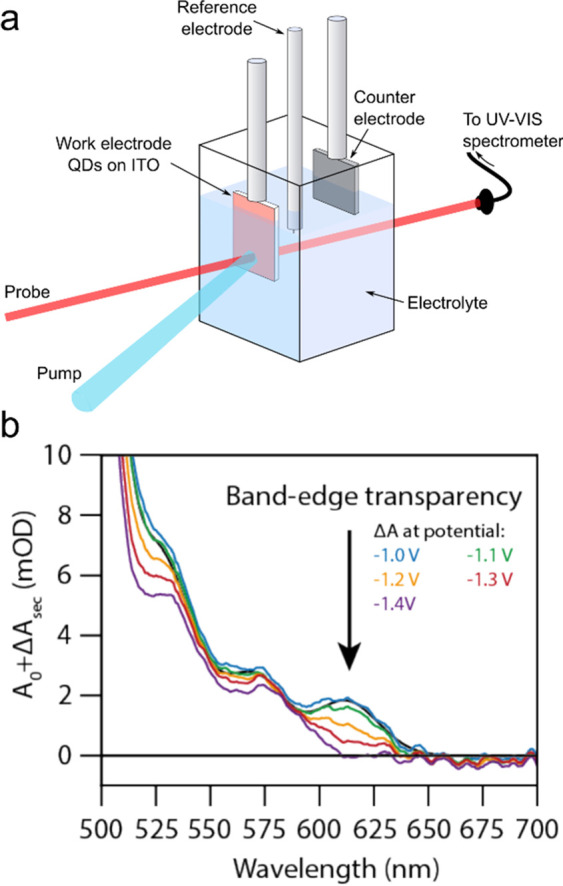
(a) A scheme of TA measurements conducted on a QD sample placed into an electrochemical cell. A QD film deposited onto a conductive substrate serves as a “work electrode”. Application of a negative potential to the work electrode versus the reference electrode leads to the injection of electrons into the QDs. The degree of QD charging is controlled by the applied voltage. “ITO” is indium tin oxide. (b) Absorption spectra of an unexcited QD film as a function of applied “negative” potential. The black spectrum corresponds to zero potential. The increase in the potential leads to progressive bleaching of the band-edge absorption feature, which occurs due to progressive filling of the 1Se state. When the potential is raised to −1.4 V, the band-edge transition is completely bleached indicating that the average number of injected electrons per dot is 2 or more. A0 is sample absorbance without charging (shown in terms of optical density). ΔAsec is the change in absorbance due to charging. Adapted with permission from ref (126) (CC BY-NC-ND).
In the experiments of ref (118), electrochemical doping was applied to CdSe nanocrystals which allowed for reducing the ASE threshold from 1 mJ cm–2 for neutral QDs to 0.3 mJ cm–2 for the charged sample (Figure 12a). More recently, the effects of electrochemical charging on QD gain properties were evaluated using TA measurements126 (Figure 12b). These studies revealed the change of the gain threshold from ⟨N⟩ = 2 in the case of the undoped sample to ⟨N⟩ close to 0 in the presence of the injected electrons (Figure 12b). The latter results indicated the realization of “zero-threshold” optical gain.
Figure 12.
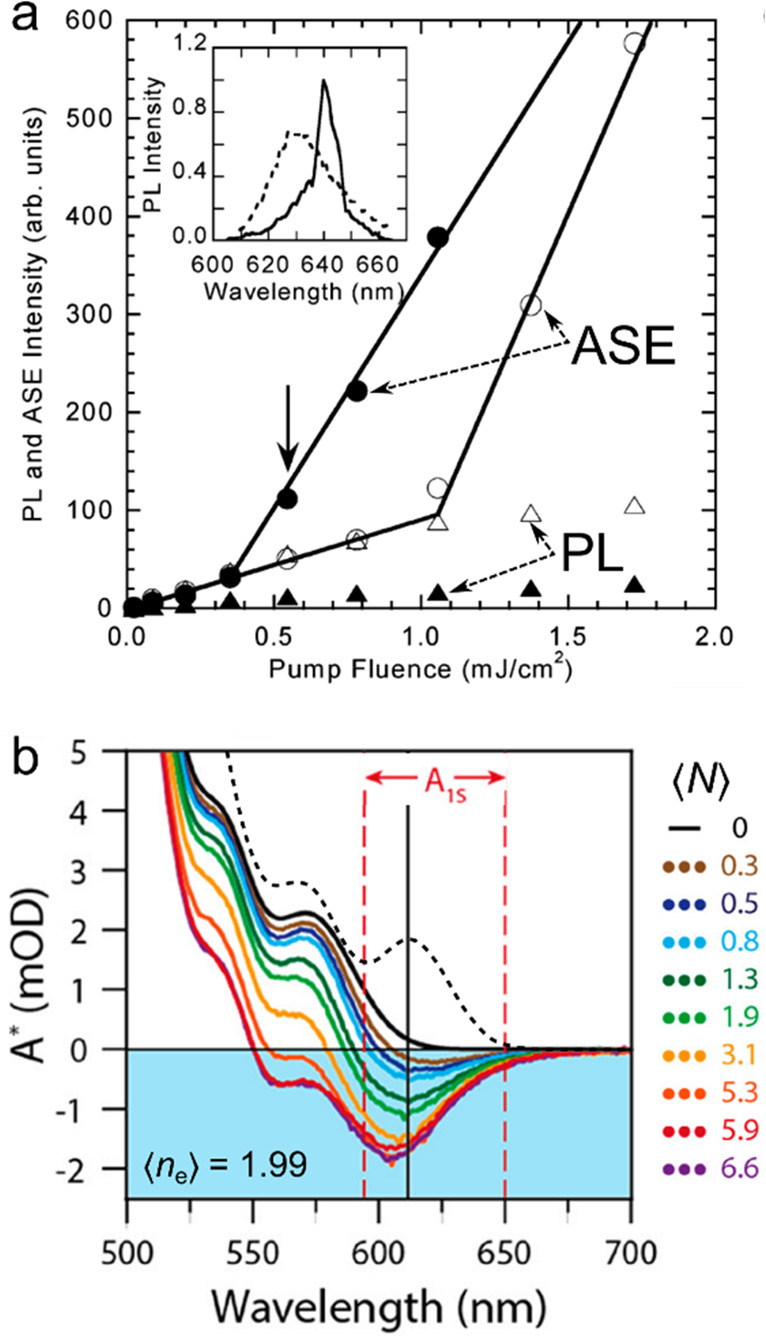
(a) The first demonstration of the beneficial effect of charging on QD optical gain properties using ASE measurements of electrochemically charged QD films.118 The plot shows the intensity of ASE of a CdSe QD film before (open symbols) and after (solid symbols) charging with extra electrons. After charging, the ASE threshold is reduced to 0.3 mJ cm–2 from 1 mJ cm–2 in the case of the neutral QDs. Inset: the emission spectra of the neutral (dashed line) and charged (thick line) samples measured at a per-pulse pump fluence of 0.54 mJ cm–2 (marked by the black arrow in main panel). The spectral shape dramatically changes upon QD charging due to the transition to the ASE regime. This regime is not apparent in the case of the neutral QDs. Adapted with permission from ref (118). Copyright 2004, American Chemical Society. (b) Excited-state absorption spectra of CdSe QDs, obtained using a TA experiment conducted on a QD sample placed into an electrochemical cell (Figure 11a). The QDs are electrochemically charged with (⟨ne⟩ = 1.99. The negative values of optical density (A*) correspond to optical gain. The onset of optical gain is observed at a very low pump power (⟨N ⟩= 0.3) indicating the realization of “zero-threshold” optical gain, as expected for the case of the doubly charged QDs (Figure 10a,b; right). The dashed black line is the linear absorption spectrum of the neutral QDs, with the vertical black and red lines indicating absorption from the 1S state (A1S). Adapted with permission from ref (126) (CC BY-NC-ND).
3.3.2. Photochemical Charging
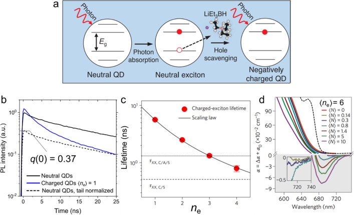
Another approach to inject long-lived electrons employs chemical reduction of photoexcited nanocrystals.127−130 In this technique, photoexcitation leads to formation of a neutral exciton. Then, the hole of the exciton is scavenged by a mild reductant such as lithium triethylborohydride (LiEt3BH) (Figure 13a). This reaction can be conducted with nanocrystals in solutions119 or applied to film samples.61,119 In particular, using a solution form of QDs and LiEt3BH as a hole scavenger, ref (119) demonstrated the possibility of producing highly charged QD states with ne up to 6. The average number of injected electrons was determined from time-resolved photoluminescence (PL) measurements, which were used to quantify the fraction of uncharged (neutral) QDs, q(0) (Figure 13b).61,119,120 This quantity was then used to obtain ⟨ne⟩ from q(0) = e–⟨ne⟩, which assumed a Poisson distribution of electrons in the QD sample.
Figure 13.
(a) The mechanism of QD photochemical charging that leads to injection of long-lived electrons. Excitation of a QDs produces an e-h pair. The hole is quenched via the interaction with a reducing agent (here LiEt3BH), which leaves behind an uncompensated, long-lived electron. Adapted with permission from ref (61). Copyright 2019, The American Association for the Advancement of Science. (b) The degree of charging, ⟨ne⟩, can be evaluated from the analysis of PL dynamics of neutral (black line) and charged QDs (blue line). In particular, by normalizing the PL trace of the neutral sample so as to match its long-time tail to that of the charged sample (dashed black line) one can quantify the fraction of uncharged QDs in the partially charged sample, q(0). This quantity is then used to determine ⟨ne⟩ (see text for details). (c) Experimentally obtained lifetimes of charged excitons as a function of ne (symbols) can be perfectly described using a statistical scaling of Auger time constants (line). (d) TA measurement of CdSe QDs in solution with ⟨ne⟩ = 6 produced by photochemical injection of electrons. Solid lines are excited-state absorption spectra (α = α0 + Δα) as a function of pump fluence for ⟨N⟩ from 0 to 10. Optical gain (α < 0) develops at the extremely low excitation level of ⟨N⟩ = 0.14 (inset), indicating the realization of the regime of “zero-threshold optical gain”. The dashed black line corresponds to the linear absorption of uncharged QDs, for reference. Panels (b–d) adapted with permission from ref (119). Copyright 2017 Nature Publishing Group.
By preparing QDs with a varied degree of charging, the authors of ref (120) measured lifetimes of a single exciton in the presence of a different number of extra electrons (τne) and then extracted the corresponding Auger time constants (τA,ne). These data were used to verify the validity of statistical scaling (eq 6) based on which 1/τA,ne ∝ ne (ne + 1).97 This expression (black trace in Figure 13c) was indeed in perfect agreement with the measurements (symbols in Figure 13c). The conducted studies also indicated that at moderate degrees of charging (ne ≤ 3 to 4), charged-exciton Auger lifetimes were longer than the biexciton lifetimes (horizontal lines in Figure 13c). This represents an important advantage of the charged-exciton gain mechanism versus the traditional biexciton mechanism.
The studies of ref (119) utilized TA measurements to evaluate the effect of charging on optical gain. These measurements revealed the reduction of the optical gain threshold to near-zero values at high degrees of charging (Figure 13d), which validated the concept of “zero-threshold” optical gain. Importantly, the experiments conducted on solid-state nanocrystal films also demonstrated the reduction of the ASE threshold due to extra electrons.
An important milestone toward practical exploitation of charged-exciton gain in lasing technologies was the demonstration of single-mode QD DFB lasers that showed strong reduction of the lasing threshold due to photochemically injected electrons.61 The reported experiments employed cg-QDs comprising a CdSe core overcoated with a thick continuously graded CdxZn1–xSe shell and a final protective layer of ZnSe0.5S0.5/ZnS. These specially engineered dots allowed for considerable suppression of Auger decay, a necessary condition for making effective use of charged excitons as optical-gain species. The cg-QDs were deposited onto a second-order DFB grating that was immersed into a solution of LiEt3BH in tetrahydrofuran (THF) (Figure 14a). The degree of charging was controlled by varying the amount of LiEt3BH. Without charging, the lasing threshold (⟨Nth,las⟩) was 1.3. Upon sample exposure to LiEt3BH, ⟨Nth,las⟩ dropped to 0.5 for 0.2 M of LiEt3BH and then, to ⟨Nth,las⟩ = 0.31 for 0.4 M of the reductant (Figure 14b). Thus, using charged-exciton gain it was possible to realize high-quality single-mode lasing (Figure 14c) with an ultralow subsingle exciton threshold, a result of considerable technological significance in the context of both optically and electrically pumped lasers (Section 6.4).
Figure 14.
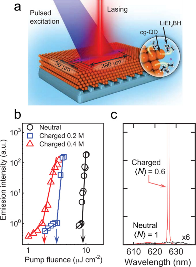
(a) The cg-QD laser prepared by depositing a cg-QD film on top of the second-order DFB grating. In this device, optical feedback is due to in-plane 2nd-order Bragg diffraction. The 1st-order Bragg scattering leads to surface emission whose direction is normal (or near-normal) to the device plane. The device is immersed into neat THF or a solution of LiEt3BH in THF. In the latter case, the dots become negatively charged under exposure to incident light. The degree of charging can be controlled by varying the amount of LiEt3BH. (b) The surface-emitted light intensity as a function of per-pulse pump fluence for varied degrees of charging (excitation by 190 fs pulses at 3.6 eV). For neutral cg-QDs, the lasing threshold (wth,las) is 9 μJ cm–2. Increasing the amount of reductant lowers wth, las until it reaches ∼2 μJ cm–2. This corresponds to the subsingle-exciton regime for which ⟨Nth,las⟩ = 0.31. (c) The spectra of surface emitted light for the neutral (black) and the charge (red) sample. The neutral sample does not show lasing at ⟨N⟩ = 1. However, after QDs are charged (⟨ne⟩ = 3.1), the device exhibits single-mode, narrow-band lasing at a subsingle-exciton pump level for which ⟨N⟩ = 0.6. All panels adapted with permission from ref (61). Copyright 2019, The American Association for the Advancement of Science.
3.3.3. Doping with Electrons via Chemical Treatments
Electrochemical and photochemical methods allow for facile, real-time control of a degree of nanocrystal charging. However, the injected electrons are not “permanent” and are quenched by, for example, exposure of nanocrystals to oxygen.61,119 Chemical doping allows one to resolve this problem by providing a tool for creating a long-lived population of uncompensated charge carriers in nanocrystal samples. In addition to the improved stability, the benefit of such permanently doped samples is the ease of their integration with devices including electrically pumped lasers (Section 6.4).
As was discussed previously, the use of charged-exciton gain would be especially beneficial in the case of nanocrystals with highly degenerate band-edge states such as those made of PbSe and PbS (Section 3.2.2). Preliminary work using In3+ substitution131 or remote electron transfer from organic molecules132 led to weak n-type doping of PbSe QDs. A more successful doping strategy was recently demonstrated in ref (133). By treating PbS QDs with iodine, the authors of that study achieved partial substitution of S2– anions for I– (presumably, occurring on the [100] facets), which resulted in heavily n-doped samples (Figure 15a). A clear manifestation of doping was the strong bleach of the band-edge absorption features. For the studied samples, they were located in the short-wave IR (SWIR) spectral range (Figure 15b). Another signature of successful doping was the emergence of a midwave IR (MWIR) absorption band due to an intraband transition between the 1Se and 1Pe electron levels.133,134
Figure 15.
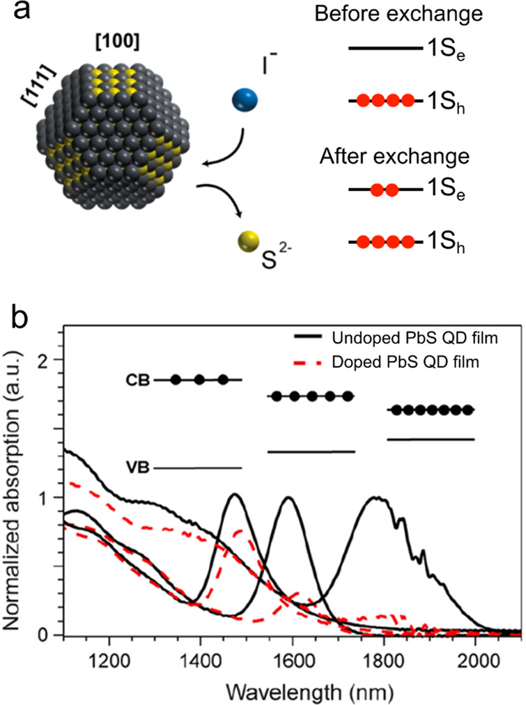
(a) Surface treatment of PbS QDs with I– ions (for example, 1-ethyl-3-methylimidazolium iodide or ZnI2) leads to substitution of S2– ions for I– on the [100] facets (left). This results in electron doping (right). (b) The absorption spectra of PbS QDs before (black lines) and after (red dashed lines) the doping procedure. The addition of extra electrons manifests as strong bleaching of the band-edge absorption peak. Larger-size QDs feature greater presence of the [100] facets. As a result, they exhibit increased levels of doping. All panels adapted with permission from ref (133). Copyright 2020 American Chemical Society.
The use of size-controlled n-doped PbS QDs allowed for demonstrating ASE tunable across the SWIR telecommunication bands (1500 to 1700 nm, Figure 16a).123,133 By varying the level of n-doping from ⟨ne⟩ = 2.7 to 4.8, the authors of ref (133) were able to tune the ASE threshold from ⟨Nth,las⟩ = 2.5 to ∼1.2 (Figure 16b). Both values are in good agreement with estimations based on eq 5, which predicts optical gain thresholds of 2.65 and 1.6 for ⟨ne⟩ = 2.7 and 4.8, respectively.
Figure 16.
(a) The ASE spectra of differently sized n-doped PbS QDs span across the S-, C-, L-, and U-bands of the telecommunication range. (b) The ASE threshold as a function of emission wavelength tuned by the QD size. The change in the QD size leads to a varied doping level (⟨ne⟩ = 2.7 to 4.8; indicated in the figure). The increase in ⟨ne⟩ leads to the reduction of the ASE threshold, as expected for the charged-exciton gain mechanism. Panels (a, b) adapted with permission from ref (133). Copyright 2020 American Chemical Society. (c) Measurements of the surface-emitted intensity of the 2nd-order DFB laser (left-top inset) based on neutral (black lines and corresponding symbols) and n-doped (red lines and corresponding symbols) PbS QDs. Samples are pumped by 300 fs, 1.2 eV pulses. The lasing threshold is appreciably reduced upon QD doping. The right-bottom inset is the lasing spectrum of the doped sample. Adapted with permission from ref (123). Copyright 2021 Springer Nature Limited.
A further advance in this area was the demonstration of DFB lasing achieved by integrating the doped PbS QDs with second-order DFB resonators (top-left inset of Figure 16c).123 Using this approach the authors of ref (123) achieved stable lasing in the range of 1550-to-1650 nm wavelengths (bottom-right inset of Figure 16c). Importantly, the comparison of undoped and doped samples showed an appreciable reduction of the lasing threshold due to doping.
The most recent development has been associated with the use of compositionally graded PbS/PbS1–xSex QDs with suppressed Auger recombination.124 These structures are analogous to compositionally graded II-VI QDs emitting in the visible,59,61 and offer similar benefits in optical gain and lasing applications but in the range of IR wavelengths. In particular, using n-doped PbS/PbS1–xSex QDs, the authors of ref (124) demonstrated low-threshold, long-lived optical gain and large net modal gain coefficients in excess of 2000 cm–1. Importantly, with these QDs, they were able to achieve lasing with a subsingle-exciton threshold ⟨Nth,las⟩ = 0.87. The tests of stability indicated that the n-type QD gain medium maintained its lasing performance for hours and, in particular, more than 80% of the power output was preserved after 8 h of operation. These results suggest that the concept of charged-exciton gain, first implemented with visible-light-emitting II-VI nanocrystals, also helps boost lasing performance of IV-VI nanostructures emitting the range of IR wavelengths.
3.4. Manipulation of Optical Gain Spectra
3.4.1. Extension of the Optical Gain Bandwidth due to High-Order Multiexcitons
A classic example of optical gain media with a broad bandwidth are organic dyes that are widely used in applications that require a readily tunable emission wavelength.135,136 Broadband optical gain materials can also enable multiband lasers and can be used in optical sensing for amplification of weak signals with unspecified wavelengths.
Up to now, in this review, we have focused on band-edge optical gain arising from the inversion of the lowest-energy transition of a nanocrystal material. As was shown in ref (137), using this mechanism it is possible to realize a certain level of control of optical gain profile by employing “state-resolved” optical pumping with a tunable laser source.137 However, the range of achieved spectral variations was fairly narrow and limited to near-band-edge spectral energies (Figure 17a).
Figure 17.
(a) Optical gain manipulation via “state-resolved” excitation of CdSe QDs. The ASE peak wavelength depends on whether the pump photon energy is tuned to the band-edge (1S) or the first excited-state (1P) transition. Adapted with permission from ref (137). Copyright 2009 American Physical Society. (b) Theoretical optical gain thresholds for the band-edge transition (1S, left) and the first excited-state transition (1P, right). The regime of transparency (optical gain threshold) realized when the probability of absorption is equal to that of stimulated emission. For the 1S and 1P transitions, it is achieved when N = 1 and 5, respectively. (c) Emission spectra of a solid-state film of thick-shell “giant” CdSe/CdS QDs as a function of pump fluence measured with 3.1 eV, 100 fs pump pulses. At lower fluences, the ASE consists of a single band at 1.99 eV, which is due to biexcitons. Two additional, higher-energy ASE bands appear at higher fluences at 2.14 and 2.34 eV. They are associated with higher-order multiexcitons and can be tentatively assigned to transitions involving the 1P and 1D electron states, respectively. The three ASE bands span the range of colors from red to green. Reproduced with permission from ref (139). Copyright 2009 American Chemical Society.
One approach to extend optical gain to higher energies is to exploit high-order multiexcitons for inverting the above-band-edge transitions. To quantify the per-dot number of excitons required to invert higher-energy transitions, we consider an electronic-state model of a spherical QD depicted in Figure 1a (right). We further take into account that optical transitions are allowed only between electron and hole states with the same quantum numbers, that is, 1Se–1Sh, 1Pe–1Ph, and 1De–1Dh. To attain the optical gain threshold for a specific transition which couples the ie electron and the ih levels, one needs to satisfy the following condition:
| 7 |
where fe,i and fh,j are single-state occupation factors, which can be obtained from fe,i = Ne,i/ge,i and fh,j = Nh,j/gh,j. Here Ne,i (Nh,j) is the total number of the electrons (holes) occupying a given level and ge,i (gh,j) is the corresponding level degeneracy.
If a QD is occupied with N excitons and N is ≤2, all carriers remain in the 1S states and fe,1S = fh,1S = N/2, as ge,1S = gh,1S = 2. Given eq 7, the 1S optical gain threshold can be derived from fe,1S + fh,1S = 1, which yields N1S,th,gain = 1 (Figure 17b, left), as expected based on our previous analysis in Section 2.2.2.
To realize 1P optical gain, one needs first to saturate the 1S electron and hole levels and then place carriers into the 1P levels. Hence, this requires N > 2. The single-state 1P occupation factors can be found from fe(h),1P = (N – 2)/6, as ge,1P = gh,1P = 6. In this case, the condition for the optical gain threshold is (N – 2)/3 = 1, which yields N1P,th,gain = 5 (Figure 17b, right). Similarly, we obtain N1D,th,gain = 13.
Based on the above considerations, the attainment of above-band-edge gain requires high-order multiexcitons, which makes its realization difficult due to acceleration of Auger dynamics with increasing N. For example, assuming the statistical scaling of Auger lifetimes presented by eq 6, we find that the lifetime of the state with N = 6, required to achieve 1P gain, is 45 times shorter that than the lifetime of the biexciton needed for band-edge gain. This implies that the realization of optical gain at above band-edge energies can be greatly simplified using QDs with suppressed Auger decay.
One such system is thick-shell “giant” CdSe/CdS QDs.138−140 As was discussed earlier in this review, the fact that these structures exhibit suppression of Auger decay motived their use in the first demonstration of cw colloidal nanocrystal lasers.60 The same feature of the “giant” CdSe/CdS QDs was also explored earlier to enact three-band ASE which spanned the range of colors from red to green and occurred due to population inversion of the band-edge and higher-energy transitions (Figure 17c).139 More recently, these dots were used to achieve ultrawide optical gain bandwidth of 700 meV141 and four-band ASE with spectral features ranging from ∼600 nm to ∼530 nm.142
Compositionally graded CdSe/CdxZn1–xSe cg-QDs, discussed in Section 2.4.1 in the context of Auger decay manipulation, are also promising systems for realizing broad-band optical gain. The TA measurements of cg-QDs are displayed in Figure 18a.143 The measured pump-fluence dependent excited-state absorption spectra indicate the emergence of multiple optical gain bands that can be associated with transitions involving the 1Se, 1Pe, and 1De electron states (Figure 18b).143 The band-edge gain feature is a doublet, which develops due to a large light–heavy hole splitting arising from asymmetric compression of the CdSe core (Figure 18b).106 Due to a wide optical gain bandwidth, the cg-QDs readily exhibit multiband ASE and lasing associated with the band-edge and excited-state transitions.59,61
Figure 18.
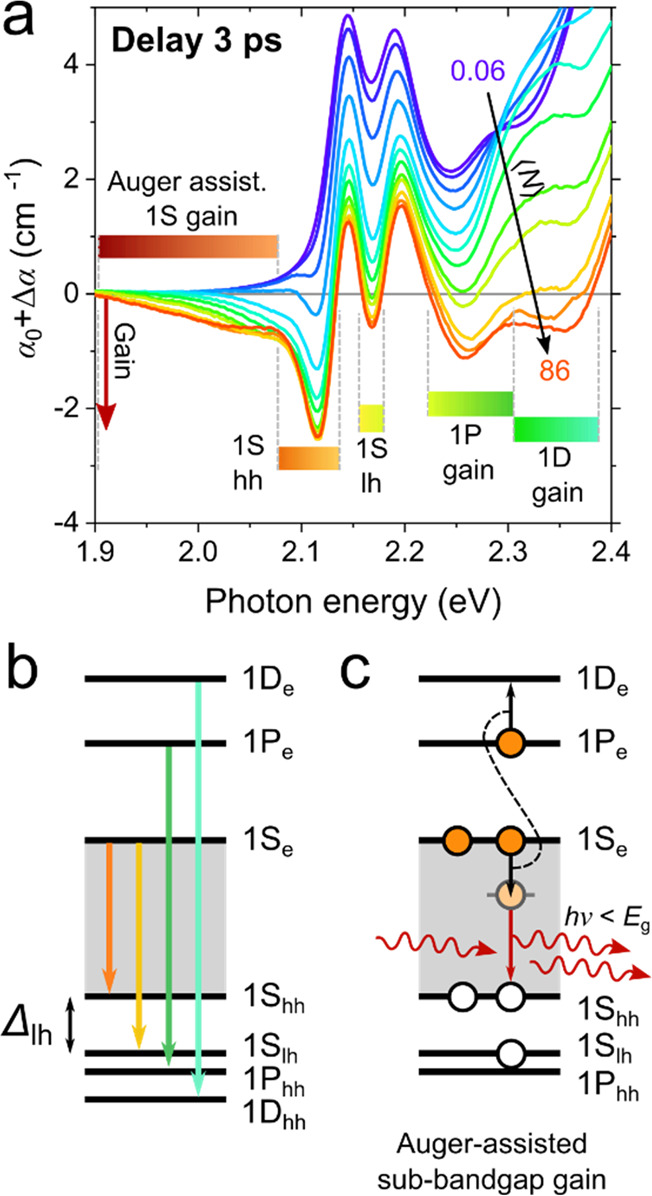
(a) Excited-state absorption spectra of cg-QDs at 3 ps after photoexcitation with short (190 fs), 2.4 eV pulses for increasing pump fluences presented as ⟨N⟩. Negative absorption corresponds to optical gain. Five gain bands are observed. Two of them, labeled as 1Shh and 1Slh, are due to the band-edge transitions involving the heavy- and light-hole states, respectively. Two higher energy bands are due to the 1P and 1D transitions. The sub-band gap feature is due to Auger-assisted stimulated emission, see panel (c). (b) The structure of the cg-QD electronic states and optical transitions responsible for optical gain features observed in the TA measurements of panel (a). (c) The illustration of Auger-assisted stimulated emission which leads to intragap gain. In this process, radiative recombination of a band-edge exciton is accompanied by re-excitation of the 1P electron to a higher-energy state, which shifts the corresponding emission band into the intragap region.
3.4.2. Sub-Bandgap Optical Gain due to Auger-Assisted Stimulated Emission
TA studies of cg-QDs143 reveal that in addition to conventional gain bands at photon energies above the bandgap, they exhibit strong intragap gain below Eg (Figure 18a).143 The pump-intensity-dependent measurements indicate that the intragap gain feature emerges at pump levels of ⟨N⟩ > 2, which corresponds to the onset of filling of the 1Pe electron state. Tentatively it was ascribed to the Auger-type process wherein the recombination energy of a band-edge e-h pair is split between an emitted photon and a 1P electron which is excited to a higher-energy state within the conduction band (Figure 18c). This process is somewhat similar to the Auger-type effect which leads to red-shifted emission bands from bulk CdS observed at high excitation intensities.144 In the case of the nanocrystal materials, it is likely unique to compositionally graded QDs that demonstrate strong suppression of nonradiative Auger recombination, which opens pathways for radiative Auger-assisted processes.
As was demonstrated in ref (143), Auger-assisted stimulated emission leads to the extension of the spectral range of optical gain to sub-bandgap energies. In particular, for the sample shown in Figure 18a, the low-energy gain cutoff occurs at ∼1.9 eV, which is 200 meV below the peak of the band-edge 1S band. Together with the higher-energy gain features, arising from the inverted 1S, 1P, and 1D transitions, this results in a large gain bandwidth of ∼500 meV.
In ref (143), the large spectral extent of optical gain was used to realize color-tunable lasing using a single cg-QD sample as an optical gain medium. In these experiments, the QDs were spin-casted onto second-order DFB gratings with periods (ΛDFB) ranging from 355 to 320 nm to obtain varied resonance wavelengths (Figure 19a). The fabricated structures were excited with short 190 fs pulses at 3.6 eV using a per-pulse fluence ramped from wp ≈ 2 to 700 μJ cm–2. The emission spectra recorded as a function of wp exhibited the emergence of a narrow feature due to single-mode DFB lasing (Figure 19a) with a well-pronounced threshold above which the emission intensity quickly grew by orders of magnitude (Figure 19b). Using gratings with different ΛDFB values, the lasing was achieved at 2.041, 2.065, 2.082, 2.099, and 2.274 eV (Figure 19a). The lowest-energy feature was due to Auger-assisted gain, while the highest-energy line was due to the inverted 1P transition. The lines with intermediate energies were due to the band-edge 1S gain.
Figure 19.
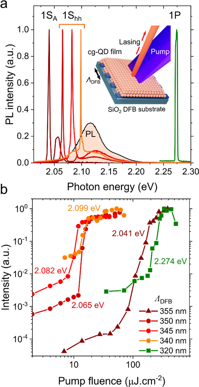
(a) Emission spectra of the 2nd-order lasers (inset) based on DFB gratings with periods (ΛDFB) from 355 to 320 nm measured using excitation with 190 fs pulses at 3.6 eV. All five lasers use the same cg-QD sample as an optical gain medium. The spectrum highlighted in pink is the spontaneous emission of the cg-QDs. The lowest-energy feature (1SA) is due to Auger-assisted optical gain. The next three higher-energy features are due to the band-edge optical gain associated with the 1Shh valence-band state. The highest-energy feature is due to the 1P transition. (b) Pump-fluence-dependent intensity of surface emission for the five lasers. Lasing thresholds span from 10 μJ cm–2 (one of the 1Shh bands) to 200 μJ cm–2 (1P band). The threshold of 1SA lasing occurs at the intermediate pump fluence of ∼50 μJ cm–2. This is consistent with the proposed mechanism, which requires excitation of a single 1P electron. 1P lasing requires that the occupancy of the 1Pe level is more than 3.
The findings reviewed in this Section point toward a considerable potential of compositionally graded QDs and other QD systems with suppressed Auger recombination as broad-band optical gain media for spectrally tunable and multiband lasers and optical amplifiers. This property mimics that of traditional laser dyes. However, as distinct from dyes, the QDs can be easily processed as solid-state films compatible with on-chip electronic and photonic circuits as well as traditional solid-state devices. This opens new areas of applications not accessible with dye solutions.
4. Novel Nanocrystal-Based Optical Gain Materials
4.1. Colloidal Quantum Wells: Nanoplatelets
4.4.1. Electronic Structures
2D colloidal NPLs have been under active investigation as optical gain materials for lasing applications.107,145−160 These structures are analogous to epitaxial quantum wells that are widely employed in present-day semiconductor lasers.161,162 Lateral dimensions of NPLs usually exceed the semiconductor Bohr radius. Therefore, carrier motion is restricted only in one dimension, namely, along the NPL thickness (referred here as the “z-axis”).47 This is expected to lead to a characteristic step-like density of states that replaces a square-root dependence typical of bulk solids (Figure 20a).
Figure 20.
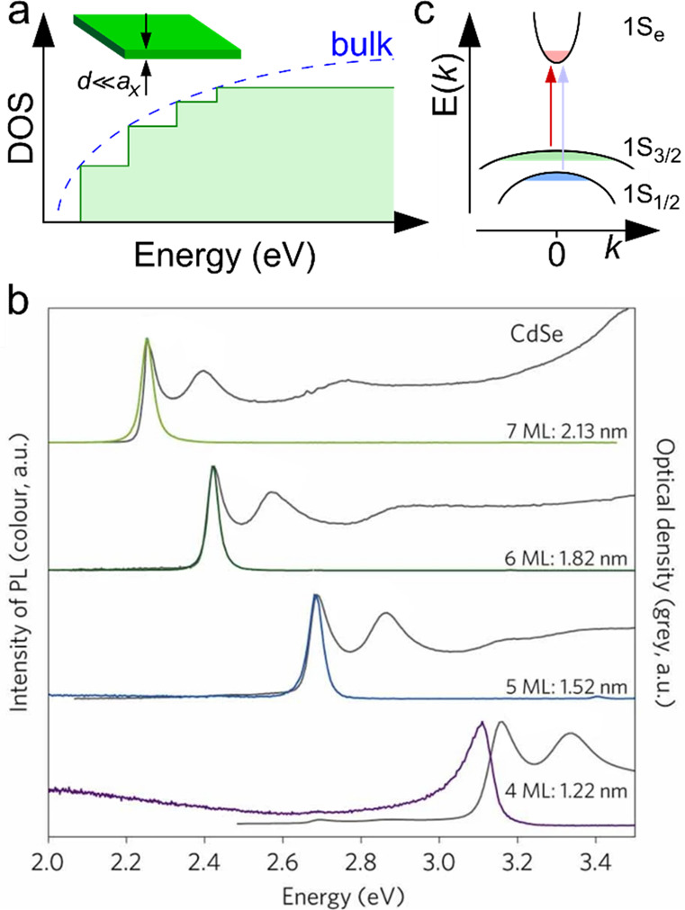
(a) A theoretical step-like density of states of a 2D quantum well (green highlight) in comparison to that of a bulk solid (dashed blue line). Inset: A schematic depiction of a NPL. Its 2D electronic properties arise from the fact that its thickness (d) is much smaller than the exciton Bohr radius (aX) of the parental bulk semiconductor. (b) Optical absorption (gray lines) and PL (colored lines) spectra of CdSe NPLs with a varied thickness. Due to strong confinement along the z-direction, the NPL band-edge absorption feature shifts to higher energies by nearly 1 eV when d changes from 7 to 4 MLs. Reproduced with permission from ref (47). Copyright 2011, Nature Publishing Group. (c) A simplified representation of the NPL band structure that features heavy (3/2) and light (1/2) valence sub-bands (E is energy and k is an in-plane wave vector).
Most advanced synthetically are CdSe-based NPLs prepared as core-only structures147,163−167 and complex heterostructures with core/shell168−172 and core/crown172−176 motifs as well as their combinations. Optical and electronic properties of NPLs can be tuned by varying their thickness (d). Using colloidal techniques, the CdSe NPL thickness can be adjusted with atomic precision between 2 and 8 complete monolayers (MLs) (Figure 20b).46,47,177,178 The CdSe NPLs also contain an additional layer of Cd atoms so as both NPL sides are Cd-terminated. Importantly, the NPL thickness is highly uniform across the entire macroscopic ensemble, which results in sharp spectroscopic features in optical spectra. The narrow peaks, typically observed in NPL absorption spectra (Figure 20b), arise from strong e-h Coulomb interactions that lead to formation of 2D excitons.163,179,180
In the case of CdSe NPLs, excitonic effects manifest as two sharp band-edge absorption features associated with e-h bound states involving heavy and light holes (Figure 20c).47 The large light–heavy hole splitting (100–200 meV)163,181,182 arises from strong shape asymmetry of these 2D structures.85,183,184 Due to strong quantum confinement along the z-axis, the NPL absorption onset and the emission band can be tuned by hundreds of meV by varying d (Figure 20b).47
4.1.2. Auger Recombination
As in 0D QDs, multiexcitons in 2D NPLs are subject to fast nonradiative Auger recombination. In the case of smaller NPL volumes (VNPL < 100 nm3), the measured biexciton Auger lifetimes scale approximately linearly with VNPL (Figure 21a),148,185 This is similar to the universal volume scaling established previously for 0D nanocrystals (Section 2.3.1),89,93 however, with a different proportionality constant (χNPL). In particular, by fitting the experimental data of Figure 21 in the range of VNPL < 100 nm3 to τA,XX = χNPLVNPL, we obtain χNPL = 2.7 ps nm–3 (red solid line), which is approximately three times as large as for 0D nanoparticles (χ = 1 ps nm–3; black dashed line). This increase is beneficial for lasing applications as multiexcitons play an important role in light amplification in the NPL systems.
Figure 21.
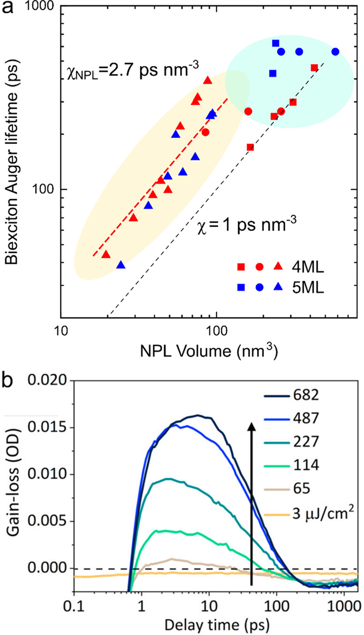
(a) Biexciton Auger lifetimes of 4- and 5-ML CdSe NPLs (red and blue symbols, respectively) as a function of NPL volume (VNPL) based on measurements of refs (148), (185), and (186) (squares, circles, and triangles, respectively). These data indicate two regimes: linear scaling with VNPL for smaller-volume structures followed by τA,XX saturation for larger-volume NPLs. The former regime is similar to that of “universal” volume scaling observed for 0D nanocrystals (τA,XX = χVNC). However, in the case of the NPLs, the proportionality constant is approximately three times as large (χNPL = 2.7 ps nm–3; red solid line) as in the case of 0D nanostructures (χ = 1 ps nm–3; black dashed line). (b) Optical gain dynamics of 4-ML CdSe NPLs as a function of excitation fluence measured using 150 fs, 3.1 eV pump pulses. Based on these data, optical gain is sustained for around 100–200 ps. Reproduced with permission from ref (158). Copyright 2019 American Chemical Society.
In the range of larger volumes (VNPL > 100 nm3), the dependence of τA, XX on VNPL weakens and according to refs (148 and 185) reaches a plateau (Figure 21a). A more complex dependence in the range of large VNPL was suggested by studies presented in ref (186). The authors of that work reported linear scaling of the Auger lifetime with the NPL area (ANPL) and approximately d7 scaling with the NPL thickness. They explained this complex behavior in terms of Auger rates controlled by the product of the ANPL-dependent frequency of exciton–exciton collisions and the d-dependent Auger recombination probability of a biexciton complex.186
Interestingly, the absolute values of biexciton lifetimes for larger-volume NPLs group near the trend line characteristic of large 0D QDs (black dashed line in Figure 21). Therefore, even in the biggest studied NPLs, the biexciton lifetime remains shorter than ∼600 ps, as in standard (nonengineered) nanocrystals. As a result, optical gain dynamics are quite fast. In particular, based on the measurements of ref (158) in the case of large-volume 4-ML NPLs (VNPL of ∼200 nm3), the optical gain lifetime is around 100–200 ps (Figure 21b).
The use of core/shell CdS/CdSe/CdS NPLs seems to lead to lengthening of Auger lifetimes. In particular, the measurements of the 4-ML CdSe core samples that comprised a 3-ML CdS shell (the core volume was ∼200 nm3) indicated the Auger time constant of ca. 400–500 ps,187 which was slightly longer than the values of ∼200 ps to ∼400 ps observed previously for core-only structures of a similar volume (Figure 21a).
Greater extension of Auger lifetime was recently reported for complex core/crown NPLs with a compositionally graded shell.160 These structures explore the “grading” strategy previously successfully applied for suppression of Auger decay in cg-QDs (Section 2.4.2).60,61 This strategy was also effective in the case of the NPLs and allowed for extending τA,XX to 750 ps for the core volume of ∼200 nm3.
In the above analysis of Auger lifetimes, we link them to the NPL volume. While this approach provides a convenient tool for rough estimations of Auger time constants, it does not separate the influence of the area and the thickness of the NPLs on Auger rates. However, in some case (for example, large-area NPLs) such separation is important. This problem has been recently addressed in ref (185), which applied atomistic, electronic-structure-based calculations to analyze surface-area- and thickness-dependent trends in Auger recombination in NPLs.
4.1.3. Optical Gain Mechanisms
Optical gain in NPLs is governed by several different mechanisms depending on NPL lateral dimensions and excitation densities.107,152,154,185 In small-area structures, the optical gain mechanism is likely similar to that in 0D nanocrystals, that is, it has a biexcitonic nature. In this case, the optical gain threshold corresponds to excitation of a single exciton per NPL on average and gain saturation occurs when the band-edge state is fully occupied, that is, the NPL is excited with two or more excitons. Thus, the optical gain properties can be described in terms of a “state-filling” model, therein, the state occupancies are controlled by the total number of e-h pair excited per NPL and states’ degeneracies (Figure 22).
Figure 22.
Three different optical gain regimes in colloidal NPLs. In smaller-area NPLs, optical gain is controlled by “state filling” as in 0D nanocrystals. In this case, optical gain threshold, ⟨Nth,gain⟩, corresponds to excitation of approximately 1 exciton per NPL on average, that is, ⟨Nth,gain⟩ ≈ 1. In larger-area NPLs, whose lateral dimensions are greater than the size of the 2D exciton (2a2D), the optical gain is controlled by effects of “space filling”. In this regime, the maximal excitonic occupancy of an NPL is defined by its area and is approximately equal to ANPL/(πa22D). The gain threshold in this case is within the range 1 < ⟨Nth,gain⟩ < ANPL/(πa22D). At high excitation levels, when the excitonic gas undergoes a Mott transition to a dense e-h plasma, the gain threshold shifts to ⟨Nth,gain⟩ > ANPL/(πa22D). In this case, optical gain occurs due to stimulated emission from the degenerate e-h plasma. Center graph reproduced with permission from ref (148). Copyright 2015 American Chemical Society.
The situation changes in the case of larger-area structures, whose lateral dimensions are greater than the size of a Coulombically bound 2D exciton (2a2D; here a2D is the 2D exciton radius). In this case, multiple excitons with identical “internal” quantum numbers can coexist in the same NPL and the maximal number of such excitons is defined not by state degeneracies but by the NPL size. Under these conditions, optical gain properties are controlled by effects of “space filling” (Figure 22), and gain characteristics, such as the gain threshold and the maximal achievable (saturated) gain, are linked to the excitonic sheet density (ρ2D).154,188 As a result, the gain threshold, expressed in terms of a per-particle excitonic number, increases with the NPL area (Figure 22).107,188
A similar increase occurs for the saturated gain coefficient. In particular, in 0D CdSe QDs, gain saturation is achieved for pump fluences that are approximately twice the gain threshold, and further growth of wp does not translate into increased band-edge gain. In contrast, as was observed in refs (157) and (187), in NPLs gain saturation does not occur until the pump fluence is approximately ten times higher than that required for the onset of gain. As a result, the band-edge gain can reach very large values exceeding 6000 cm–1 (Figure 23a).157 Very large gain coefficients in NPL materials have been observed in multiple studies utilizing both VSL experiments146,149,150,156,187 and TA measurements.107,152,154,155,160,189 In addition to the high NPL excitonic occupancies needed for gain saturation, large optical gain coefficients result from extremely high packing densities achievable with the NPLs (Figure 23b).153
Figure 23.
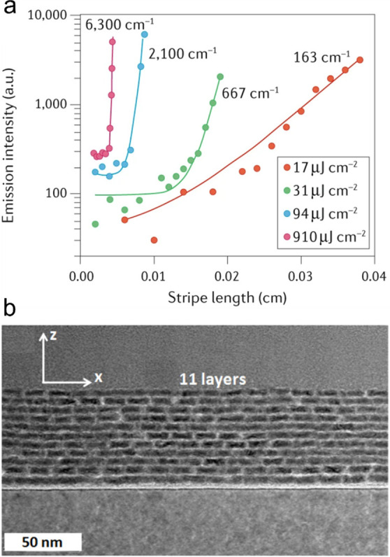
(a) Room-temperature VSL measurements of optical gain in 4 ML-CdSe-NPL film using excitation fluences ranging between 17 and 910 μJ cm–2 (150 fs, 400 nm pulsed excitation). At the highest pump level, the modal gain coefficient reaches a very high value of 6300 cm–1. Adapted with permission from ref (157). Copyright 2019 American Chemical Society. (b) A solid-state film made of 11 layers of 4-ML CdSe NPLs with a Cd0.25Zn0.75S alloyed shell. This image illustrates that NPLs are capable of forming very dense solids, which helps boost optical gain. Adapted with permission from ref (153). Copyright 2020 American Chemical Society.
As was suggested in refs (154) and (190), in addition to excitonic states, NPLs may support stable Coulombically bound biexcitons or excitonic molecules. Due to reduced dielectric screening, typical of 2D structures,191,192 in thin NPLs, the biexciton binding energy can reach large values of around 30–40 meV that are greater than the room-temperature thermal energy (∼25 meV). As a result, a photogenerated e-h system may represent a mixture of unbound excitons and excitonic molecules both of which can contribute to optical gain.154,190
Yet another gain mechanism emerges at high excitation densities when 2D excitons start to overlap and an electron loses its association with a specific hole, which leads to exciton dissociation. This situation corresponds to a Mott transition from an excitonic system to a dense e-h plasma.193−195 The critical sheet density of the Mott transition (ρ2D,Mott) scales approximately as 1/(πa22D). When the carrier concentration in the plasma state reaches the condition of degeneracy (ϕe + ϕh = 0, see Section 3.2.2), the probability of stimulated emission becomes equal to that of optical absorption, which corresponds to the onset of optical gain (Figure 22).
Stimulated emission by the degenerate e-h plasma is the most common optical gain mechanism in traditional semiconductor lasers based on both bulk and quantum-well materials.196−199 This mechanism has been also realized in colloidal NPLs. In particular, in a recent study described in ref (107), 4-ML CdSe NPLs showed two different optical gain regimes with two distinct spectral bands (Figure 24). One band, located below the band-edge transition, emerged at ∼25 μJ cm–2 (or ⟨N⟩ of ∼4), and it was assigned to excitonic molecules (Coulombically bound biexciton states). The other shorter-wavelength gain feature developed at higher pump fluences (⟨N⟩ of ∼35) and it was explained it terms of stimulated emission from a degenerate e-h plasma.
Figure 24.
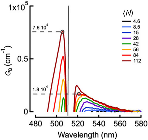
Optical gain spectra of 4-ML CdSe NPLs (ANPL ≈ 340 nm2) as a function of average NPL excitonic occupancy.107 These spectra were recorded using a TA experiment for a pump–probe delay of 2.5 ps using excitation with 100 fs, 3.1 eV laser pulses. At lower excitation levels, optical gain occurs in the sub-bandgap region (520–560 nm). It was ascribed to excitonic molecules. The second gain band emerges at higher pump levels (⟨N⟩ > 35). It was located in the range of the above band gap energies and explained by stimulated emission from the degenerate e-h plasma. Here, gain is presented as a bulk-equivalent gain coefficient, GB (Section 3.1.1). Adapted with permission from ref (107). Copyright 2019 American Chemical Society.
While not being discussed in ref (107), radiative exciton–exciton scattering, well-known for bulk semiconductors,144 in principle, could also contribute to intragap gain. In this process, one exciton collapses radiatively by transferring part of its energy to the second exciton. As a result, the emission line becomes red-shifted with regard to the exciton energy. This effect is similar to Auger-assisted emission in nanocrystals discussed in Section 3.4.2 and it, in particular, is also driven by Auger-type Coulombic collisions between photoexcited carriers.
4.2. Beyond II-VI Semiconductors: Perovskite Nanocrystals
4.2.1. Optical-Gain-Related Properties of Perovskite Nanocrystals
Solution-processable perovskites prepared as both bulk films and nanocrystals have recently emerged as promising optical-gain materials.24,200−202 While both systems showed laser action under optical excitation, the observed ASE and lasing thresholds were lower for nanocrystals,24 as expected for 0D structures wherein optical gain threshold can be achieved with just one e-h pair excited per particle (Section 2.2.2). As discussed earlier, additional beneficial features of the nanocrystalline materials are facile spectral tunability of an emission wavelength achieved via particle size control and a weak sensitivity of optical gain to variations in temperature.32,37 The latter simplifies the realization of ASE and lasing at room temperature, a necessary requirement for technologically viable light-amplification devices.
The primary focus on the optical gain and lasing studies of perovskites nanocrystals has been on lead halide structures with the general formulation APbX3. Their crystal lattice is composed of two interpenetrating cubic sublattices, one of which comprises [PbX6]4– octahedra (X = Cl, Br, or I), and the other, inorganic or organic A+ cations (Figure 25a). A very popular perovskite system is all-inorganic CsPbX3 nanocrystals44 first reported in 2015. As synthesized, these are cubically shaped particles of fairly large dimensions of ∼10 nm and more (Figure 25a).44,203,204 Since these sizes are comparable to the exciton Bohr diameter in these materials (∼10 to ∼24 nm; ref (44)), the range of spectral tunability via size control is fairly limited. However, the bandgap of the CsPbX3 nanocrystals can be readily tuned over a wide range of energies by adjusting the composition of a halide component (Figure 25b).44 This can be done via straightforward anion exchange procedures,205−207 using which one can obtain mixed halide compositions and thereby continuously tune the emission wavelength (Figure 25b). This a convenient capability for prospective lasing applications as it allows one to obtain shorter-wavelength emission with fairly large particles that are less affected by Auger recombination (see below).
Figure 25.
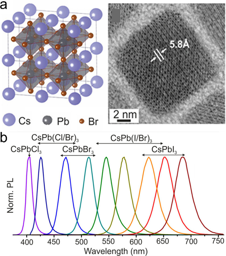
(a) Left: A schematic depiction of a crystal structure of a CsPbBr3 perovskite that comprises two interpenetrating cubic sublattices formed by PbBr6 octahedra and Cs ions. Right: a high-resolution transmission electron microscopy image of an individual cubically shaped CsPbBr3 nanocrystal with a cube side of ∼13 nm. Based on well-resolved lattice fringes, the lattice constant is 5.8 Å, which is the same as for the bulk crystal. (b) The PL spectra of a series of CsPbX3 nanocrystals with a varied composition of a halide component demonstrate wide-range spectral tunability which covers the entire range of visible wavelengths. All panels reproduced with permission from ref (44). Copyright 2015 American Chemical Society.
As nanocrystals of more traditional compositions, perovskite nanocrystals exhibit volume scaling of Auger lifetimes.99,100,208,209 As was discussed earlier in this review (Section 2.3.1), this scaling is functionally similar to that observed, for example, for II-VI CdSe nanocrystals; however, the proportionality constant is different. In particular, based on the analysis of smaller-size particles (Figure 4, green line), χ ≈ 0.06 ps nm–3, which is more than an order of magnitude smaller than that for CdSe nanocrystals (Figure 4, orange line). As a result, the Auger lifetimes for the same-size particles are considerably shorter, which is detrimental for lasing applications, especially in the case of devices with cw optical and direct current (d.c.) electrical pumping (Sections 2.3.3 and 5.3). An additional problem is that the existing strategies for Auger decay engineering via heterostructuring and compositional grading (Section 2.4.2) are difficult to apply to perovskite nanocrystals as they exhibit high ionic mobility that tends to homogenize the composition across the entire particle.210,211
However, there are still approaches to achieve certain control of Auger lifetimes beyond that due to “volume scaling”. In particular, Auger rates seem to be sensitive to the composition of both the anion and cation components.100,209,212 For example, it was observed that τA,XX becomes longer when the anion is switched from Cl to Br and then I.99,100,209 Another reported observation is the effect of an A-site cation on Auger time constants. In particular, the replacement of Cs with organic cations such as methylammonium or formamidinium led to a 5-fold increase of the Auger lifetime.212 Based on these insights, the use of I-based structures with organic A-site cations may help alleviate (at least partially) the problem of fast Auger decay in perovskite nanocrystals.
Another important parameter for applications in optically pumped lasers is an absorption cross-section. Previous studies established that the nanocrystal absorption cross-section at energies well above the band gaps scales linearly with the nanocrystal volume: σabs(hν) = fcorVNC(nNC/nm)αbulk(hν), where nNC and nm are, respectively, the refractive indices of the nanocrystal material and the external medium, αbulk(hν) is the bulk absorption coefficient, and fcor ≤ 1 is the field correction factor determined by a “dielectric contrast” at the nanocrystal/external-medium interface.39,89 Interestingly, although the particle volumes of typical CsPbBr3 nanocrystals are larger than those of spherical CdSe QDs,100 this does not translate into a proportional enhancement of σabs. In fact, based on the measurements described in ref (100), the absorption cross-section of CsPbBr3 nanocrystals with a VNC of 250 nm3 was similar to that of 48 nm3 CdSe QDs100 despite a more than 5-times greater volume. Based on the analysis of dielectric parameters of CsPbBr3 and CdSe, the authors of ref (100) concluded that the reduced absorption cross-sections of perovskite nanocrystals stemmed from a lower absorption coefficient of bulk CsPbBr3 that was likely approximately ten times lower than that of CdSe.
4.2.2. Optical Gain Mechanism, and ASE and Lasing Experiments
An important parameter of a material from the standpoint of optical gain applications is the degeneracy of band-edge states, which defines their occupancy limits and thereby optical gain thresholds and the magnitude of saturated gain. The states’ degeneracies are defined by factors such as the number of equivalent band minima in the Brillouin zone and the spin structure of CB and VB states. As distinct from II-VI semiconductors whose CB and VB minima are at the center of the Brillouin zone (Γ-point),83,213,214 the band minima of CsPbX3 perovskites are located at the R-points.215,216 The Brillouin contains 8 equivalent R-points. However, since they are shared between 8 primitive cells, this does not increase the degeneracy factor and all R-points can be treated as a single band minimum.
Further complexities arise from a mixed 5p(halide)/6s(Pb) character of the VB,44,215 and spin–orbit coupling (SOC).100,215−217 Without SOC, three degenerate sub-bands may coexist at the CB minimum.215−218 However, if SOC is taken into consideration, the number of CB degenerate sub-bands can be reduced to 2 or even 1, depending on specific assumptions.215,217,218 In this case, the final CB state degeneracies would be 4 and 2, respectively (Figure 26a).
Figure 26.
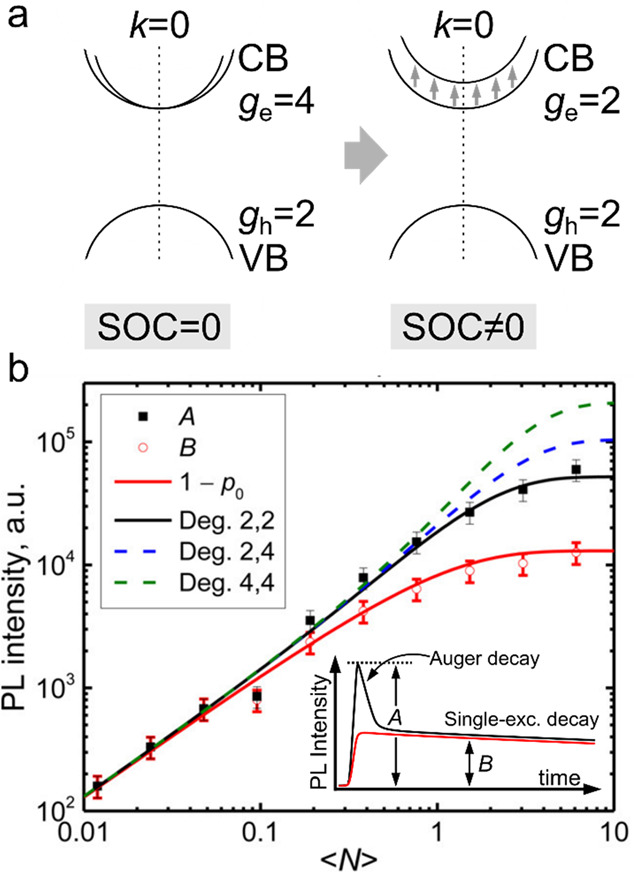
(a) An approximate band diagram of a CsPbX3 perovskite without (left) and with (right) inclusion of effects of spin–orbit coupling (SOC). If one accounts for splitting of the CB states due to SOC, the CB band-edge degeneracy is reduced from 4 to 2. (b) The early- and late-time PL signals (A and B, respectively) of the CsPbBr1.5I1.5 nanocrystals as a function of ⟨N⟩ obtained from the PL time transients (inset) recorded using excitation with 3.6 eV, 220 fs pulses. At large ⟨N⟩, when both signals are saturated, their ratio is controlled by the degeneracies of the CB and VB states that define their maximal occupancies. Based on the conducted modeling, the measurements are best described assuming ge = gh = 2 (black solid line). The dashed lines show modeling for gmin = 2 and gmax = 4 (blue), and gmin = gmax = 4 (green). Here, gmin = min(ge, gh) and gmax = max(ge, gh). The red line is calculated from (1 – p0), there p0 is the fraction of unexcited nanocrystals obtained using Poisson statistics of photon absorption events. Adapted with permission from ref (100). Copyright 2016 American Chemical Society.
To shed light onto this subject, the study presented in ref (100) employed TA and transient PL experiments to elucidate occupancy limits of the band-edge states of CsPbX3 nanocrystals. Based on these measurements, the saturation of the band-edge TA and PL signals occurred when two or more excitons were excited per nanocrystals (Figure 26b). This indicated that both the CB and the VB states were 2-fold degenerate, that is, ge = gh = 2. This further suggested that optical gain is governed by the same principles as those for a simple two-level system comprising 2-fold spin-degenerate states (Section 2.2.1). In particular, the optical gain threshold is given by ⟨Nth, gain⟩ = 1, and gain saturation occurs that when all nanocrystals contain biexcitons and other higher-order multiexcitons, that is, ⟨N⟩ ≥ 2.
The reported studies of ASE219−223 and lasing24,25,219,221,222,224 using perovskite nanocrystals are consistent with the biexcitonic gain mechanism. The measured band-edge optical gain coefficients of close-packed films reach ∼450 cm–1,24,219,223,225 which is on par with values observed for CdSe-based systems.119,226 The optical gain lifetimes (∼100 to ∼600 ps)220,227 are also similar to those of nonengineered CdSe nanocrystals.
As was indicated earlier, an interesting capability associated with perovskite nanocrystals is spectral tunability achievable via composition control. This capability was exploited in ref (24) to demonstrate multicolor ASE using CsPbX3 nanocrystals with a varied halide composition (Figure 27). In particular, with purely Br-based structures, the ASE occurred at ∼540 nm (green color). By using a mixed Br/Cl system with increasing Cl content, the ASE band was gradually shifted to 470 nm (blue color). When Br was mixed with I, the ASE shifted toward longer wavelengths reaching eventually ∼630 nm (red color).
Figure 27.
(a) Pump-fluence dependent emission spectra of a close-packed film of CsPbBr3 nanocrystals excited with 400 nm, 100 fs pulses. The fluence was tuned from 3 to 25 mJ cm–2. The sharp feature emerging on the longer-wavelength side of the recorded spectra is due to ASE. (b) An illustration of spectral tunability of ASEachieved by adjusting the composition of the halide component. All panels reproduced with permission from ref (24) (CC-BY 4.0).
In addition to demonstrations of cavity-free ASE, multiple works have combined perovskite nanocrystals with different types of optical resonators to realize laser oscillations. These include vertical cavity surface emitting lasers (VCSELs),25,222,228 devices based on whispering gallery mode structures,24,219,224 and lasers employing Fabry–Pérot resonators.229 An interesting recent study described in ref (230) demonstrated ASE-active waveguides prepared as free-standing, flexible, water-resistant membranes composed of functionalized perovskite nanocrystals and a cellulose acetate polymer.
5. Principles of Nanocrystal Laser Diodes
5.1. Challenges of Laser Diodes
A laser diode is an EL device wherein an electric current is converted into emitted laser light. This makes it similar to a traditional LED. However, there are critical distinctions between the two devices that make the realization of a laser diode considerably more difficult than an LED. A typical QD LED features a p-i-n architecture wherein a thin, 1–2 monolayer QD film is sandwiched between an n-type electron and a p-type hole transport layer (ETL and HTL, respectively) (Figure 28). This design alleviates the problem of poor charge conductance of a QD solid and facilitates injection of both types of carriers under forward bias and minimizes device current under reverse bias.
Figure 28.
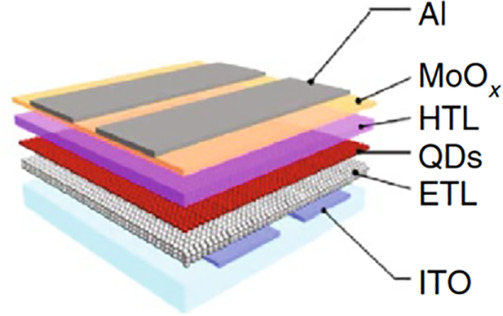
A schematic depiction of a typical “inverted” QD LED. It comprises an active QD layer sandwiched between ETL and HTL, supplemented by a cathode and an anode. In the present example, the two latter elements are made of an ITO layer and an Al/MoOx bilayer. Reproduced with permission from ref (56) (CC-BY-NC-ND).
A nanocrystal-based laser diode can be thought of as an LED-like device with an addition of an optical resonator. This resonator can be implemented either as an internal (integrated) or external optical cavity that circulates light through the nanocrystal-based gain medium and leads to its amplification via stimulated emission (Figure 29). One challenge in realizing this structure is the need for effective mitigation of damping of cavity modes due to optical losses in various charge conducting layers of an EL device stack. A further problem is potential disruption of charge injection pathways caused by the integrated optical resonator. An additional complication is the need for extremely high current densities (j) required to first achieve optical gain and then realize a gain coefficient that is sufficiently high to compensate for optical losses in a complex device stack.
Figure 29.
A schematic depiction of a nanocrystal laser diode. This device can be thought of as a nanocrystal-based LED that contains an optical cavity for circulating light through an active nanocrystal-based optical gain medium. In the displayed scheme, the cavity is formed by optical reflectors 1 and 2. As in a standard LED, in a laser diode, electrons and holes are injected from the opposite sides of the nanocrystal layer via a combination of appropriate charge-injection/transport layers. The charge-injection architecture must be capable of delivering very high j necessary to generate optical gain in the nanocrystal medium. In the case of charge-neutral nanocrystals, the values of j must be sufficiently high to generate biexcitons at least in a fraction of the particles in the active volume.
5.2. Laser Diodes versus LEDs
In a traditional QDLED, a QD is excited via sequential injection of negative and positive charges. In an “inverted” LED with a ZnO ETL, the first step is electron injection, which can occur even spontaneously (without bias) due to a high Fermi level of n-type ZnO.56 The second step is hole injection, which leads to creation of a neutral exciton. Importantly, this step is favored over injection of the second electron because of Coulombic effects (Figure 30). Coulombic attraction facilitates injection of a charge of the opposite sign, while the injection of the same-sign charge is inhibited by Coulombic repulsion. The model of ordered (“correlated”) injection in QD LEDs was first introduced in ref (59) and recently validated by experiments presented in refs (231) and (232). Following the creation of an exciton, the QD emits a photon and thereby returns to its ground state. Thus, in a standard LED, the QD is circulated between the ground (|0⟩), negatively charged (|e–⟩), and single-exciton (|X⟩) states. In Figure 30 this excitation/relaxation cycle is shown by blue shading.
Figure 30.
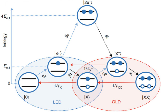
In a standard “inverted” LED, a QD is excited by the injection of an electron, followed by the injection of a hole. The latter process is facilitated by Coulombic attraction that favors the injection of a positive charge (energy downhill process). Simultaneously, Coulombic repulsion impedes the injection of the second negative charge (energy uphill process). The net result of these two injection steps is the creation of an exciton. It recombines to emit a photon, which brings the QD back to the ground state. Then, this cycle (shown by blue shading) repeats again. Labels |0⟩, |e–⟩, and |X⟩ denote the ground, single-electron, and single-exciton states; ge and gh are the rates of electron and hole injection, respectively. The vertical axis shows electrostatic energies of different QD states computed using a model of a charged sphere.15 In this model, the electrostatic energy of a doubly charge QD is 4 times greater than the energy of the singly charged dot (Ec,1). In order to realize optical gain, a QD must be excited with a biexciton. This requires a different excitation/relaxation cycle (red shading) in which the QD is circulated between the single-exciton, negatively charged-exciton (|X–⟩, negative trion), and biexciton (|XX⟩) states. The lifetimes of these states are τX, τX– and τXX. “QLD” is the abbreviation for “QD laser diode”. Reproduced with permission from ref (15). Copyright 2021 Springer Nature Limited.
The realization of laser action requires a different excitation/relaxation cycle (highlighted by red shading in Figure 30 and label “QLD”, which stands for “QD laser diode”). Optical gain relies on biexcitons. To generate a biexciton, the exciton created via electron and hole injection steps needs to be excited further to a negative-trion state instead of letting it relax to the ground state. Afterward, the trion must be quickly converted (before recombination) into a biexciton via hole injection. Then, the biexciton relaxes to the single-exciton state via stimulated emission, which concludes in the QLD cycle. Apparently, the realization of this cycle requires high injection rates that must outpace decay of both single excitons and trions. Further, to allow for accumulation of sufficiently large number of biexcitons, the injection rate must also be higher than the biexciton recombination rate. Since both trions and biexcitons are subject to fast Auger recombination, the realization of the QLD excitation/relaxation cycle (red shading in Figure 30) is considerably more difficult than the realization of the traditional LED cycle (blue shading in Figure 30). In particular, as discussed in the next Section, this requires very high current densities that greatly exceed those used in standard QD LEDs.
5.3. Optical Gain and Lasing Thresholds in Electrically Pumped Devices
To quantify current densities required to achieve optical gain and laser action, we will use the model of Figure 30 in which we assume that the rates of electron and hole injection are equal to each other (gexc,e = gexc,h = gexc) and further disregard the injection pathway, which involves a doubly charged QD (dashed arrows in Figure 30). In this case, d.c. electrical injection can be treated as cw optical excitation analyzed by us earlier using a three-state model of Figure 2b. In order to apply the results of this analysis to electrically pumped devices, we need to relate the excitation rate to current density. For this purpose, we will use an electrical cross-section (σe) introduced previously in refs (15) and (32). This quantity defines an affective area from which a QD collects charge carriers flowing through the device.
Intuitively, σe is directly linked to the QD cross-sectional area, which we will refer to as a QD geometrical cross-section, σg = πR2. However, in a typical LED device setting, σe can be greater than σg. To illustrate this, we will consider an EL device, which contains a single layer of QDs sandwiched between an ETL and an HTL. Due to an organic capping layer and unbound ligands present in the QD film, the areal filling factor (fa) of QDs can be considerably lower than 1. In fact, based on the available literature,32,59fa is ca. 0.5–0.6 for large core/shell particles (R = 7–10 nm) typically used in QD LEDs. The rest of the film is filled with insulating molecules. As a result, the current flows preferentially through QD semiconductor cores that serve as “current-focusing” apertures (Figure 31). Because of this effect, the electrical cross-section is increased compared to σg by a factor of 1/fa, that is, σe = σg/fa.
Figure 31.
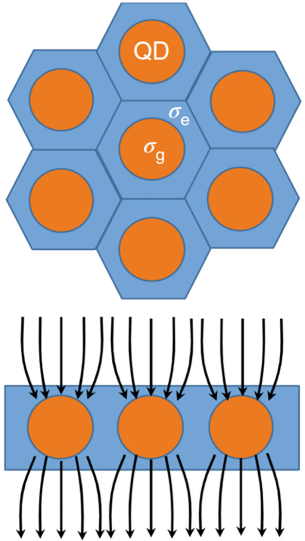
In a film sample, semiconductor QDs (orange) are surrounded by bound and unbound organic ligands that form an insulating barrier (blue). As a result, electric current (black arrows) is funneled through semiconductor particles that act as “current focusing” apertures. Because of this effect, the electrical cross-section of a QD (σe) is greater than its geometric cross-section (σg). Reproduced with permission from ref (15). Copyright 2021 Springer Nature Limited.
Using the electrical cross-section, we can relate the excitation rate to the current density by gexc = σe(j/e), where e is the elementary charge. This further allows us to convert gexc,th,gain and gexc,1/2 obtained earlier in Section 2.3.3 into corresponding current densities:
| 8 |
| 9 |
Here, as in the case of optical pumping, j1/2 is used as an approximate measure of the lasing threshold.
First, we will use eqs 8 and 9 to compute threshold current densities for standard nonengineered CdSe QDs with a 2.5 nm radius used in our earlier estimations of optical gain and lasing thresholds in the case of cw optical pumping. We will use the same time constants (τX = 20 ns, τXX = 65 ps) and assume fa = 0.5. For these parameters, jth,gain = 0.36 kA cm–2 and j1/2 = 6.3 kA cm–2. These values are orders of magnitude higher than maximal current densities realized in standard d.c. QD LEDs, for which the device breakdown usually occurs at j of ∼1 A cm–2.233,234 This emphasizes again the need for specially engineered QDs with a suppressed Auger recombination and an increased electrical cross-section for lowering jth,gain and j1/2 to levels compatible with colloidal nanostructures.
Luckily, compositionally graded cg-QDs, discussed earlier in the context of optically excited lasers, are also well suited for applications in electrically pumped lasing devices. Indeed, due to a large type-I shell they have large electrical cross-sections. Simultaneously, they exhibit a strong suppression of Auger decay leading to a long τXX. These improvements translate into a considerable reduction of jth,gain and j1/2. In particular, using parameters of cg-QDs from ref (59) and fa = 0.5 in eqs 8 and 9, we obtain jth,gain = 7 A cm–2 and j1/2 = 24 A cm–2. While both current densities are still high by standards of traditional QD LEDs, they can be easily realized using devices with a special “current-focusing” architecture.59 In fact, the values of j can be pushed much higher (to 100s of A cm–2 and even to more than 1000 A cm–2) using devices wherein current focusing is combined with pulsed electrical pumping.16,62 In the next Sections, we will discuss implementations of nanocrystal-based optical-gain and lasing devices.
6. Electrically Excited Optical Gain and Lasing
6.1. Optical Gain in High Current Density LEDs
6.1.1. Design Principles of Nanocrystal Laser Diodes
Nanocrystal-based LEDs have been realized using particles of various morphologies including 0D QDs34,56,235,236 and 2D NPLs.237,238 The majority of these studies have utilized II-VI-based nanocrystals (primarily CdSe34,56,239). More recently, high-performance LEDs based on III-V (mostly, InP236,240,241) nanocrystals and perovskite nanostructures242,243 have been reported in the literature. At present, this is a mature field with good prospects for commercialization in the near future.101,236,244,245
As discussed earlier (Section 5.1), the realization of nanocrystal-based laser diodes is considerably more challenging than the realization of standard LEDs. First, it requires specially engineered nanocrystals that feature strong suppression of Auger recombination and large optical gain cross-sections. Additional challenges lie in the areas of electrical and optical designs of the device structure. In particular, the charge injection architecture must be capable of generating high current densities necessary for inverting the nanocrystal gain medium. Simultaneously, the same device must feature low optical losses so they would not suppress the gain generated in a thin active medium. Finally, the realization of laser oscillations requires an optical cavity, which should be integrated so as not to disrupt charge-injection pathways. Below, we discuss practical approaches for addressing these challenges.
6.1.2. Mechanisms for Degradation at High Current Densities
The realization of laser diodes, and high-j devices in general, requires effective heat management as heat accumulation causes several issues affecting device stability. In particular, the generated heat leads to distortion of a nanocrystal passivating layer and thereby degradation of the emission efficiency.246 Further, the rise in device temperature increases unwanted optical losses in charge-conducting layers, which leads to the reduction of net optical gain.62,247 The excess heat can also compromise the integrity of charge-conducting layers and thereby lead to device breakdown.
The elements that are especially sensitive to effects of heat are organic charge-transport layers (CTLs) often used as HTLs.34,248 In particular, the properties of organic materials are dramatically modified when they reach the glass transition temperature (Tg), which typically ranges from 100 to 150 °C.249 During this transition, the material switches from a glass- to a rubber-like phase.250 As a result, it becomes softer and more sensitive to heat-induced degradation.251,252 This also reduces the material’s electrical strength making it more prone to electrical shorts.253
This implies that the realization of high-j devices requires HTLs with high Tg values. For example, popular HTLs based on 4,4′-bis(N-carbazolyl)-1,1′-biphenyl (CBP)254 and N,N′-bis(naphthalen-1-yl)-N,N′-bis(phenyl) benzidine (NPB)255 are not well suited for this purpose as they have fairly low Tg values of 62 and 98 °C, respectively. More suitable alternatives are N,N′-bis(naphthalen-1-yl)-N,N′-bis(phenyl)-2,7-diamino-9,9-spirobifluorene (Spiro-NPB) or Tris (4-carbazoyl-9-ylphenyl) amine (TCTA) whose Tg values are 126 and 151 °C, respectively.256 Due to their higher thermal stability, inorganic HTLs may also be considered for implementing high current density LEDs.239,257
Understanding device overheating under high current densities and the development of methods for mitigating this problem are important components of efforts aiming at the development of colloidal nanocrystal laser diodes. Next, we overview a simple quantitative model of device overheating and experimental approaches to reduce it.
6.1.3. Modeling of Device Overheating
To model heat accumulation in an active volume of a nanocrystal-based LED, we consider the interplay between heat generation due to Joule heating and heat dissipation via thermal exchange with the environment.15,258 In our modeling, we will neglect temperature gradients within the active volume, which will allow us to characterize it by a spatially uniform temperature Td. To describe heat outflow, we will treat a surrounding environment as an ideal heat sink with temperature T0. Under these conditions, the time-dependent device temperature can be described by
| 10 |
where C is the heat capacity
of the active volume, ΔT = Td – T0, Ad is the active area, V is the applied
voltage, and K is the heat exchange constant. In
the case of d.c. current when  , eq 10 leads to the following expression for device overheating
| 11 |
According to eq 11, overheating can be reduced by boosting the heat exchange constant for enhancing heat dissipation and/or decreasing the size of the injection area for reducing the overall amount of generated heat. The former of these measures can be implemented using, for example, special substrates with high heat conductivity,259,260 and the latter, by employing so-called “current-focusing” approaches for reducing the injection area.261,262
Further reduction of overheating is possible by using excitation with short, widely spaced pulses. Pulsed excitation aims to switch off Joule heating before the device reaches the steady state temperature defined by eq 11. In addition, the device can cool down during interpulse periods, potentially to the temperature of the environment. To elucidate the dynamics of device temperature in the case of pulsed excitation, we assume that the applied bias is a square-shaped waveform with pulse duration τp, amplitude V0, and pulse-to-pulse separation Tpp. Using this waveform in eq 10, we obtain
| 12 |
where τT = C/K is the characteristic heat-dissipation time constant. In the short-pulse limit (τp ≪ τT), this expression yields
| 13 |
which implies that using pulsed pumping, one can reduced device overheating by a factor of τp/τT compared to the d.c. case.
In the next two Sections, we consider practical implementations of current-focusing and pulsed excitation schemes that have been applied to realize high-j nanocrystal LEDs.
6.1.4. Current-Focusing Approaches
To realize current-focusing, one can reduce the injection area using specially shaped electrodes and/or small apertures inserted into an electron and/or hole injection path.59,258 This method helps reduce heat inflow by reducing overall current flowing through the active volume and simultaneously it facilitates heat exchange with the environment. As a result, current-focusing devices can tolerate higher current densities without breakdown.263,264
A current-focusing structure can be realized using orthogonal electrodes (an anode and a cathode) shaped as narrow strips whose overlap defines a small injection area.261,265 Another approach is to employ a small aperture in an insulating interlayer (made of, for example, SiO2, LiF, or Al2O3) inserted into a device stack on one of both sides of an active nanocrystal layer.147,266
The first report on electrically excited nanocrystal gain59 employed a current-focusing device based on compositionally graded cg-QDs wherein a charge-injection area was defined by a narrow slit (<100-μm-wide) in a 50 nm-thick LiF insulating interlayer. The developed structures were able to reach current densities of 18 A cm–2 under d.c. excitation59 (Figure 32a). At j > 3–4 A cm–2, in addition to traditional band-edge EL, they exhibited the second higher-energy EL feature involving the 1Pe electron state (Figure 32b). This observation implied that the 1Se state was completely filled, which further suggested that the QDs were occupied with at least 2 excitons per dot on average. This was above the optical gain threshold (∼1 exciton per dot) and, in fact, indicated complete saturation of band-edge optical gain.15,59
Figure 32.
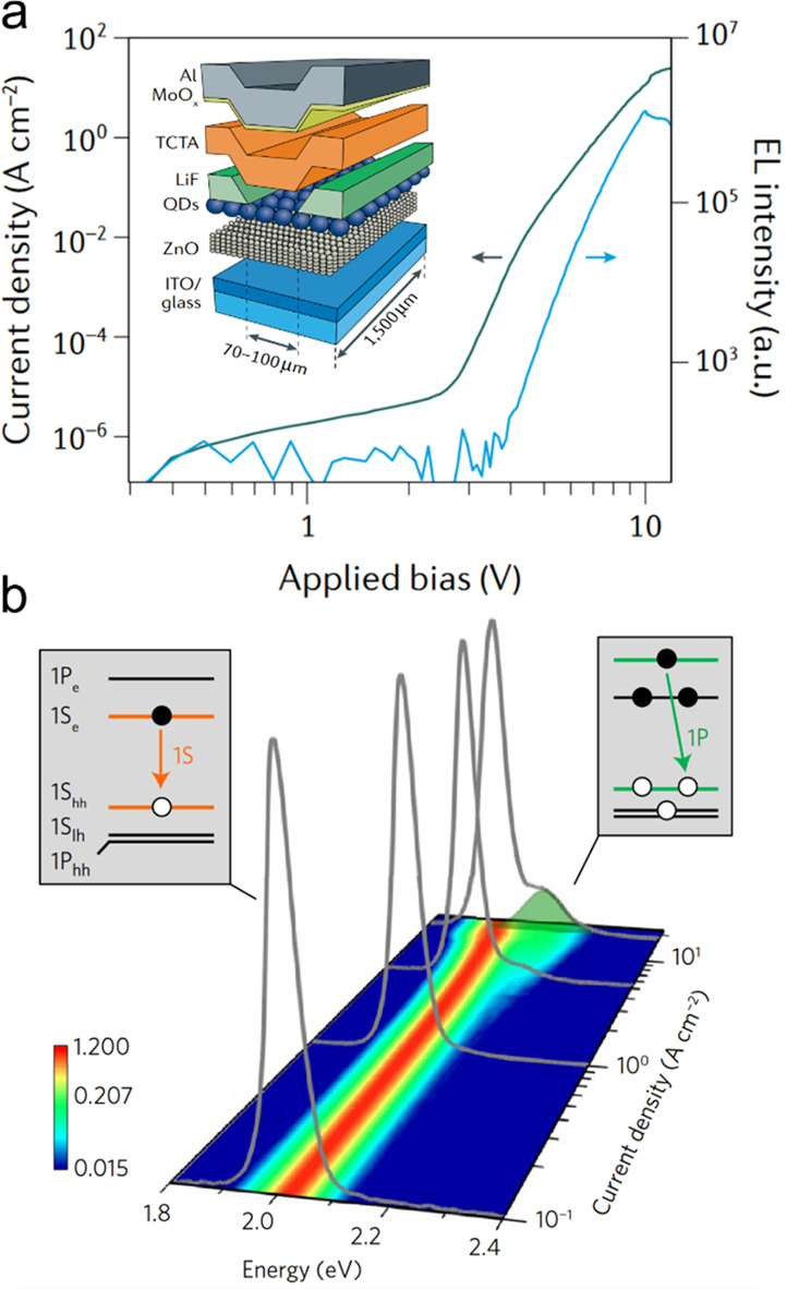
(a) The plots of the j–V and the EL-intensity–V dependence of a current-focusing LED employing compositionally graded CdSe/CdxZn1–xSe-based cg-QDs with suppressed Auger recombination.59 The maximal current density reaches 18 A cm–2, which is considerably higher than in standard QD LEDs. Inset shows the device structure which features a dielectric LiF interlayer with a narrow current-focusing slit. (b) The EL spectra measured for increasing current density reveal the emergence of the higher-energy 1P emission band, which indicates that the band-edge 1S state is fully occupied, that is, the dot contains at least two excitons (insets). All panels adapted with permission from ref (59). Copyright 2018 Springer Nature Limited.
6.1.5. Pulsed Excitation
As was demonstrated in ref (16), the current density can be pushed to very high values (∼1000 A cm–2) by combining a current-focusing architecture with pulsed excitation. In devices reported in that work, the injection area was reduced by a factor of ∼10 compared to that in ref (59) using 2D current-focusing implemented with a combination of a slit-like aperture and an orthogonal narrow metal anode. An additional distinction from the previous study was the use of pulsed excitation with pulses as short as 1 μs, which corresponded to the duty cycle of 0.1% for the 1 kHz repetition rate (Figure 33a). The pulsed pumping helps reduce heat inflow and simultaneously enhances heat dissipation due to long cooling periods separating adjacent voltage pulses. Previously, this approach was applied in organic28,262,265 and perovskite267,268 high-brightness LEDs as well as traditional laser diodes based on epitaxial QDs.269,270
Figure 33.
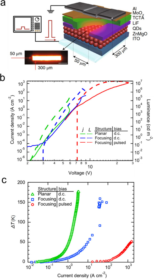
(a) A device stack of a high-j cg-QD LED employing 2D current-focusing. The image of the emitting area (bottom left) shows that the injection area is limited to 50 μm by 300 μm. (b) The j–V and L–V plots (L is luminance) for the current-focusing device (blue and red lines) in comparison to those of the reference (planar) device without current focusing (green lines). For the current-focusing device, the measurements were conducted using d.c. (blue lines) and pulsed (red lines) excitation. In the pulsed mode, the current-focusing device reached j of more than 1 kA cm–2, which resulted in unprecedented luminance of over 107 cd m–2. (c) Device overheating (ΔT) as a function of j for the planar LED under d.c. excitation (green triangles) and for the current-focusing device under d.c. (blue squares) and pulsed (red circles) excitation. These data were obtained based on the spectral shifts of the band-edge EL band. All panels adapted with permission from ref (16) (CC-BY 4.0).
The pulsed current-focusing LEDs described in ref (16) showed stable operation at ultrahigh current densities of up to ∼1000 A cm–2 and reached unprecedented brightness levels of ∼107 cd m–2 (Figure 33b). The analysis of temperature-induced shifts of the EL spectra confirmed that these parameters were achieved due to strong suppression of overheating of the active device volume16 (Figure 33c).
The effect of pulsed pumping on device overheating was experimentally investigated in ref (16) using pulses of a varied duration (1 to 30 μs) and fixed Tpp = 1 ms. For a given input electrical power (defined as Pe = V0jAd), longer pulses led to a higher temperature of the active region (Figure 34a). The overheating of the active volume, inferred from the redshift of the 1S EL band, was compared with modeling using the formalism described in Section 6.1.3. In particular, eq 10 was used to calculate average overheating during the electrical pulse (ΔTavg) as a function of input power and pulse duration. Then, by adjusting parameters K and C, the simulated ΔTavg/Pe-vs-τp dependence was matched to the measurements (Figure 34b). This procedure yielded K = 4.8 × 10⁻³ W/K and C = 1.9 × 10⁻⁸ J/K.
Figure 34.
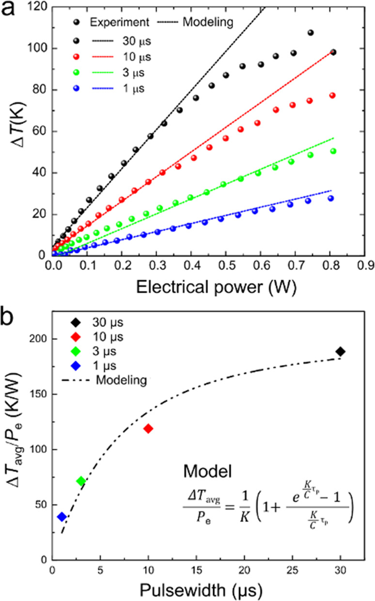
Experimental (symbols) and calculated (lines) results for device overheating of an active QD layer in a pulsed LED as a function of input electrical power (Pe) for pulse widths 30 μs (black), 10 μs (red), 3 μs (green), and 1 μs (blue). There is good general agreement between the measurements and the calculations. The deviation observed for longer pulses at higher powers is likely due to the onset of a glass transition in the organic HTL that slows down the growth of the temperature in the experimental measurements. (b) ΔTavg/Pe as a function of pulse width. ΔTavg/Pe is derived from the linear part of the ΔT-vs-Pe dependence in panel (a). The symbols are the experimental results, and the line is the modeling using eq 10. Based on the modeling, K = 4.8 × 10⁻³ W/K and C = 1.9 × 10⁻⁸ J/K.
Based on the above values, heat dissipation time constant τT = C/K = 3.9 μs. Using it, we estimate that the reduction in overheating achieved with 1 μs pulses versus the d.c. case is ∼75% (obtained from eq 13). This explains why the same device can be operated at considerably higher current densities in the pulsed mode compared to d.c. excitation. In particular, as was demonstrated in ref (16), the use of 1 μs pulses allowed to push j to over 1000 A cm–2, which was ∼30 times higher than with d.c. pumping (Figure 33b).
6.1.6. Electrically Excited Optical Gain
As discussed earlier, the first demonstration of electrically excited optical gain employed d.c. LEDs with 1D current focusing that produced j values of up to 18 A cm2.59 The active LED layer was made of compositionally graded CdSe/Cd1–xZnxSe-based cg-QDs with suppressed Auger recombination. Optical gain was detected and quantified using a current-modulated transmission spectroscopy (Figure 35a). In this experiment, optical transmittance of an operating device was probed with a color-tunable laser light. The difference in the device optical absorbance (Δα) for situations with and without bias was measured as a function of j. At sufficiently high current densities, the bias-induced absorption bleach observed below the 1S feature exceeded linear absorption (α0), which indicated the realization of optical gain (Figure 35b). The optical gain band (shown by gray shading in Figure 35b) spectrally overlapped with the biexciton emission spectrum (blue line in Figure 35b), as expected for the traditional biexcitonic gain mechanism.
Figure 35.
(a) A schematic depiction of a current-modulated transmission spectroscopy experiment. Top: An output of a spectrally tunable laser is modulated with a mechanical chopper. The “chopped” beam is used to probe the transmittance of the QD layer, which is measured as a function of applied bias. Bottom: The difference in the transmitted light intensity with and without bias is used to infer bias-induced change in the absorption coefficient (Δα). If Δα is negative and its magnitude is greater than the absorption coefficient of the unbiased device (|Δα| > α0), this implies the realization of optical gain. (b) The excited-state absorption spectrum (α = α0 + Δα; red line) obtained using bias-induced Δα (j = 8 A cm–2) in comparisons to the absorption spectrum of the unbiased device (black line). The optical gain part of the excited-state absorption spectrum (corresponds to α < 0) is highlighted by gray shading. The blue dashed line is the biexciton emission band (labeled “XX”). Panels (a, b) are adapted with permission from ref (59). Copyright 2018 Springer Nature Limited. (c) The EL spectra of the current-focusing device of ref (16) measured for varied j (the spectra are normalized so as to match the 1S-peak amplitudes). These spectra show the emergence of the higher-energy (1P) emission band, which eventually outshoots the 1S band. (d) The 1S and 1P band intensities extracted from the EL spectra in “a” (symbols) in comparison to the results of simulation (lines) conducted using the correlated-injection model presented in refs (16) and (59). According to the modeling the per-dot excitonic occupancy reaches ∼7 at j of ∼1 kA cm–2. This is sufficient to realize both 1S and 1P optical gain (pink and green shadings, respectively). Panels (c, d) adapted with permission from ref (16) (CC-BY 4.0).
A more recent generation of nanocrystal-based optical gain device reported in ref (16) employed 2D current focusing in combination with short-pulse pumping. This approach allowed for boosting j to ∼1000 A cm2, which resulted in the unusual EL spectra wherein the higher-energy 1P emission was more intense than the band-edge 1S band (Figure 35c). Based on the analysis of the 1S and 1P EL intensities using a “correlated-injection” model,16,59 the QD occupancies reached very high levels of ∼7 excitons per dot on average, which was sufficient to realize both 1S and 1P optical gain (Figure 35d).
The QD excitonic occupancy can be also estimated from the ratio of the 1P and 1S EL intensities (I1P/I1S). For this purpose, we assume that all QDs in the active volume are uniformly populated with N excitons. We further consider the regime of steady state excitation which holds true even in the case of pulsed pumping if the pulse duration is much longer than the exciton lifetime. In this situation, the EL intensity of a given QD transition is defined by its total emission rate (ri), where i = 1S and 1P. The emission rate can, in turn, be linked to the occupancy of the corresponding electron (Ne,i) and hole (Nh,i) states and a nominal emission rate per a single spin-allowed transition (r0) by ri = r0Ne,iNh,i/gi, where gi is the i-state degeneracy (2 and 6 for the 1S and 1P states, respectively). If N > 2, the 1S electron and hole states are fully occupied (that is, Ne,1S = Nh,1S = 2), and the rest of the carriers are forced into the 1Pe,h states (Ne,1P = Nh,1P = N – 2). The corresponding emission rates are r1S = 2r0 and r1P = r0 (N – 2)2/6, which yields I1P/I1S = r0 (N – 2)2/12.
Applying the derived expression to the situation where the intensity of the 1S EL is equal to that of the 1P EL, we obtain (N – 2)2/12 = 1, which yields N ≈ 5.5. This corresponds to the point of crossover of the 1S and 1P dependences in Figure 35d, which occurs at j ≈ 800 A cm2. Since N of 5.5 is above the theoretical gain threshold for the 1P transition, condition I1P = I1S may serve as an experimental indicator that the device reaches the regime of not only 1S but also 1P optical gain. We would like to point out that the above estimations are of approximate character as they neglect the complexities of a VB of real-life semiconductors such as the existence of multiple hole sub-bands.
6.2. Control of Optical Losses
6.2.1. Manipulation of the Refractive Index Profile
Even though the devices reported in refs (15), (16), and (59) indicated the realization of strong optical gain in the nanocrystal medium, they did not exhibit ASE or lasing, suggesting that the gain coefficient was lower than total optical losses and, therefore, net optical gain was negative. There are multiple sources of optical losses in the LED device stack including charging-injecting electrodes and various charge-transport layers. In particular, indium tin oxide (ITO) layers have been widely used as transparent electrodes. ITO, however, has a large absorption coefficient that exceeds 600 cm–1 in the range of visible wavelengths (αITO = 652 cm–1 at 600 nm, ref (271)). This problem is further exaggerated by its high refractive index (nITO = 1.8, ref (271)) due to which the electric field tends to concentrate in the ITO layer. This not only increases optical losses but also leads to the reduction of the mode confinement factor for the active nanocrystal layer, which lowers modal gain (Section 3.1.1). Similar effects occur due to other charge-conducting layers of the EL device.
To overcome the above problems, one needs to carefully design the cross-sectional profile of the refractive index so as to minimize the presence of the electric field in the lossy conducting layers and concurrently maximize the field confinement factor for the nanocrystal-based optical gain medium. To accomplish these objectives, the study in ref (272) utilized not regular but low-index ITO (L-ITO) prepared by mixing ITO with SiO2. This allowed for lowering the refractive index (nL-ITO = 1.6 at 630 nm, ref (272)), which resulted in the improved field distribution across the device. For the standard ITO, more than a third of the total optical-mode energy resided in the transparent electrode (ΓITO = 34%, Figure 36a).272 In the L-ITO-based device, ΓL-ITO dropped to 22%. Simultaneously, the mode confinement factor for the nanocrystal layer increased from 18% to 23% (Figure 36b). An additional advantage was the reduced absorption coefficient, which dropped by a factor of 3 for the 2:1 SiO2:ITO mixture compared to standard ITO (Figure 36c).
Figure 36.
(a) A schematic depiction of a conventional LED device employing a standard ITO electrode. The optical-field intensity profile of the fundamental transverse electrical (TE) mode is shown by the red line. Mode confinement factors for each layer are indicated in the figure. (b) Same for the device employing L-ITO. In this case, the TE mode center is shifted toward the QD layer, leading to an enhanced ΓNC. (c) Absorbance spectra of a film of standard ITO (black line) and L-ITO (red line) for the identical film thicknesses of 150 nm. The L-ITO film is prepared by mixing standard ITO with silica in the proportion 1 to 2. Adapted with permission from ref (62). (d) Optically excited lasing in the LED-like device with the 2nd order DFB grating engraved into the L-ITO electrode. Panels (a, b, d) reproduced with permission from ref (272) (CC-BY 4.0).
Using the above approach the authors of ref (272) achieved optically excited DFB lasing from a nearly complete device stack that missed only a top hole-injecting metal electrode (Figure 36d). This device had an LED-like design and comprised a DFB grating engraved into the L-ITO bottom electrode, a ZnO ETL, an active medium comprising 3 monolayers of cg-QDs, and a TCTA HTL (inset of Figure 36d). Upon application of the top molybdenum oxide/aluminum (MoOx/Al) contact, the device behaved as a standard LED that showed bright EL under electrical excitation. However, additional optical losses induced by the top electrode resulted in the suppression of lasing. The quenching problem was resolved in the follow-up studies17,62,63 discussed later in this review.
6.2.2. Analysis and Mitigation of Optical Losses
In addition to the electrodes, CTLs also contribute to optical losses. Many reported nanocrystal-based LEDs employ a ZnO ETL prepared by colloidal or sol–gel methods.16,56,235 This material is highly transparent and shows the absorption coefficient of only a few inverse centimeters in the range of visible wavelengths (e.g., αZnO = 4.6 cm–1 at 610 nm; ref (273)). Therefore, it does not contribute significant optical losses. However, due to its high refractive index (nZnO = 2 at 600 nm; ref (274)), it may lead to unwanted distortions of the optical-field distribution within the device.
Another common element of nanocrystal LEDs is a hole-injection layer (HIL) made of MoOx. As distinct from ZnO, this material is optically lossy (αMoOx = 3153 cm–1 at 600 nm, ref (275)), which was one the reasons causing quenching of lasing described in ref (272) after the deposition of the MoOx/Al contact. HTLs made of organic molecules such as TCTA are normally optically transparent. However, as was observed in ref (62), optical losses dramatically increased after TCTA was combined with MoOx (Figure 37, top). A similar enhancement in absorption was reported for other HTL materials such as CBP and NPB.276 The exact origin of this effect is yet to be understood. Tentatively, it was ascribed to the enhanced free-carrier absorption due to the increased doping associated with charge migration across the MoOx/HTL interface.276,277
Figure 37.
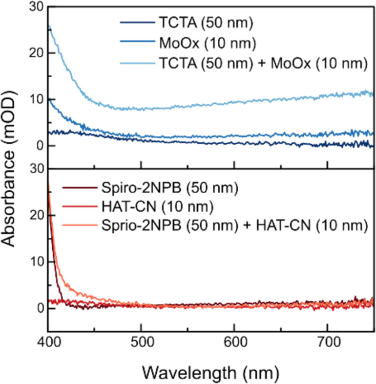
Top: The linear absorption spectra of the TCTA and MoOx films (50 and 10 nm thicknesses, respectively) and the TCTA/MoOx bilayer often used as an HTL/HIL combination in conventional QDLEDs. Bottom: Same measurements for the Spiro-2NPB HIL and HAT-CN HTL. The use of latter materials allows for considerable reduction of optical losses. Reproduced with permission from ref (62) (CC-BY 4.0).
To tackle the problem of high optical losses arising from MoOx and MoOx/HTL junctions, the authors of refs (17) and (62) employed HIL made of 1,4,5,8,9,11-hexaazatriphenylenehexacarbonitrile (HAT-CN). This organic material was previously used in high-performance nanocrystal-based LEDs.278 It exhibits good optical transparency and does not cause any increase in absorption if interfaced with organic HTLs such as TCTA, NPB, or spiro-2NPB (Figure 37, bottom).62 Therefore, it is well suited for implementing optical gain devices including laser diodes.
Considerable losses may also arise from metal electrodes due to their very high absorption coefficients.136,279,280 For instance, the absorption coefficient of silver (Ag) is of the order of 105 to 106 cm–1 in the visible spectral range (αAg = 8.4 × 105 cm–1 at 600 nm, ref (281)). Similarly high absorption coefficients have gold (αAu = 6.8 × 105 cm–1 at 600 nm, ref (281)) and aluminum (αAl = 1.3 × 106 cm–1 at 600 nm, ref (281)), both of which are also often used as electrodes. High values of α have a detrimental effect for lasing, especially if an optical mode exhibits considerable leakage into the metal contact.272
To gain a deeper insight into optical losses due to a metal layer, the authors of ref (62) analyzed the effect of a silver electrode on propagation of transverse electric (TE) and transverse magnetic (TM) modes in a glass/dielectric/Ag waveguide. This modeling utilized a photonic simulation package of COMSOL.282Figure 38 shows 2D maps of the optical fields of fundamental TE0 (panel “a”) and TM0 (panel “b”) modes. These modes showed a notable difference in the electric-field cross-sectional distributions. The TE mode was distributed fairly uniformly across the entire thickness of the dielectric layer. In contrast, the TM mode was localized near the Ag interface and propagated in a waveguide as a surface plasmon polariton. As a result of strong coupling to the metal layer, the TM mode experienced much greater optical losses than the TE mode, which led to considerably stronger attenuation during the propagation in the waveguide (Figure 38c). This implies that the TE mode is more suitable for realizing laser action than the TM mode.
Figure 38.
(a) Spatial distribution of the TE field (Ez) of the TE0 mode (λ = 600 nm) propagating in a planar glass/dielectric/Ag waveguide. The metal layer tends to expel the optical field as a result of which a photonic mode propagates primarily through a low-optical-loss dielectric layer. (b) A spatial distribution of the TM field (Hz) of the TM0 wave propagating in the same waveguide. The wave propagates along the metal surface as a “lossy” plasmonic mode. (c) Decay of the optical field intensity for the TE0 and TM0 modes during propagation in the waveguide. Adapted with permission from ref (62) (CC-BY 4.0).
While the TE-polarized optical mode is less influenced by the metal electrode than the TM mode, it is still subject to appreciable attenuation during propagation in a metal-cladded waveguide (Figure 38c). Previously, this problem was mitigated (at least partially) by inserting a dielectric spacer between the electrode and the nanocrystal layer.273 Another approach explored in the literature is to use graphene electrodes in place of metal layers.283,284 In addition to its good conductivity, a graphene layer is extremely thin (∼3.5 Å thickness) and, therefore, does not introduce considerable absorption losses.285 The use of graphene allowed for demonstrating fully transparent nanocrystal LEDs wherein both an anode and a cathode were graphene-based283 (Figure 39a).
Figure 39.
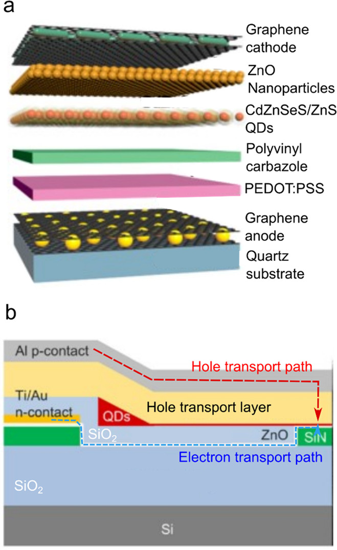
(a) An LED employing graphene layers as both an anode and a cathode. The device stack has the following structure: quartz substrate/graphene/poly(3,4-ethylenedioxythiophene) polystyrenesulfonate (PEDOT:PSS)/polyvinylcarbazole/CdZnSeS/ZnS QDs/ZnO nanoparticles/graphene. Reproduced with permission from ref (283). Copyright 2018 American Chemical Society. (b) A “remote-electrode” approach for suppressing quenching induced by the metal electrode. In this structure, the Ti/Au electron-injecting electrode is laterally displaced from the QD emitting region. The Al hole-injecting contact is followed by a thick hole transport layer. Electrons are delivered via a horizontal charge-transporting channel made of ZnO (depicted as a thin white layer). Blue and red dashed lines are electron and hole transport paths, respectively. Adapted with permission from ref (273). Copyright 2021 Wiley-VCH GmbH.
The “graphene-contact approach” was also recently exploited for demonstrating optically excited ASE in a fully stacked nanocrystal-based LED device.284 The authors of ref (284) employed a thin PbS/ZnO nanocrystal blended layer as a gain medium. It was sandwiched between an ITO cathode and a graphene anode. This device showed EL under electrical excitation and ASE under pulsed optical pumping. Electrically excited ASE, however, was not realized due to insufficiently high current densities. Therefore, the utility of graphene electrodes in ultrahigh-j optical gain and lasing devices is still an open question.
Yet another approach to mitigate losses associated with metal contacts is to laterally displace an active light-emitting region from one or both electrodes. An example of a such “remote electrode structure” is presented in Figure 39b.273 In this design, an electron-injecting contact and the active QD region do not overlap vertically but are rather connected by a CTL which serves as a lateral channel for delivering charges from the electrode to the active medium. As a result, light propagation in the active layer occurs without interference from the metal contact. However, the implementation of this design in the case of high-j devices might be challenging due to a long carrier-transport path and correspondingly high resistivity, which could result in increased device overheating.
6.3. Optically Excited Lasing in High Current Density EL Devices
6.3.1. Optical Gain Optimization
As discussed earlier in this review (Section 3.1.1), the material gain coefficient can be presented as a product of the gain cross-section and the nanocrystal concentration in an active medium (Gmat = σgainρ). For type-I nanocrystals, for which an electron and a hole are colocated in the same domain of the nanostructure (e.g., a QD core in a core/shell structure), the strength of optical transitions is virtually independent of nanocrystal size,85 implying that σgain is also not strongly dependent on particle dimensions. Thus, one approach to boost optical gain of a close-packed film is to reduce the nanocrystal size and thereby increase ρ as it scales approximately as 1/VNC.
The effect of the nanocrystal size on Gmat was experimentally studied in refs (17) and (62) using a series of CdSe/CdxZn1–xSe/ZnSe0.5S0.5/ZnS cg-QD samples with a fixed core radius of ∼2.6 nm and a varied thickness of the graded layer (HCdZnSe) that was changed from 2 to 6 nm17,6262 (Figure 40a). Using this approach, the overall cg-QD size was tuned from 12 to 20 nm, which corresponded to the change of VNC by a factor of ∼4.6. Material gain was quantified using a VSL technique (Figure 40b). The measured values of Gmat showed the expected trend, that is, the 1/VNC scaling of the gain coefficient with QD volume (Figure 40c). For the thickest graded layer, the band-edge gain coefficient (Gmat,1S) was ∼200 cm–1, and it was boosted to ∼800 cm–1 for the sample with the thinnest shell (red circles in Figure 40c). The observed increase in Gmat,1S was consistent with the expected 4.6-fold increase in the QD packing density.
Figure 40.
(a) The internal structure of a compact compositionally graded CdSe/Cd1–xZnxSe/ZnSe0.5S0.5/ZnS ccg-QD (top) along with an approximate band structure (bottom right) and an exemplary transmission electron microscopy image (bottom left). (b) Variable stripe length measurements of optical gain of a thick close-packed film of ccg-QDs (symbols) and fitting curves assuming exponential growth of the ASE intensity (lines). Based on the fits, the 1S and 1P material gain coefficients are 780 and 890 cm–1, respectively. (c) The 1S (red circles) and 1P (green squares) material gain coefficients of compositionally graded cg-QDs as a function of overall diameter; the QD size is tuned by varying the thickness of the Cd1–xZnxSe graded layer. The corresponding biexciton lifetimes are indicated next to the data points. All panels adapted with permission from ref (62) (CC-BY 4.0).
The conducted measurements also revealed a similar trend for 1P optical gain (Gmat,1P; green squares in Figure 40c). For HCdZnSe = 2 nm, Gmat,1P reached a very high value of ∼890 cm–1 (Figure 40c). Importantly, all studied samples, including those with the thinnest graded layer, showed strong suppression of Auger recombination comparable to that of the original cg-QDs59,61 (Figure 40c). Further in this review, the cg-QDs with HCdZnSe < 3 nm will be referred to as compact cg-QDs or ccg-QDs. An example of these structures is depicted in Figure 40a.
6.3.2. Optically Excited ASE and Lasing in Fully Stacked High-j LEDs
By combining optical gain/loss optimization strategies discussed earlier in this review, the authors of refs (17) and (62) demonstrated devices that performed as high-j LEDs and simultaneously exhibited ASE and lasing under pulsed optical excitation. These devices had several distinctions from both standard “inverted” LEDs34,56 as well as advanced ultrahigh-j devices.16 In particular, the developed device stack comprised a low-optical-loss L-ITO electrode that was immediately followed by a ccg-QD active layer without an intermediate ZnO ETL (Figure 41). A further distinction concerned a hole-inject part that featured an HTL made of 2,2′,7,7′-tetrakis[N-naphthalenyl(phenyl)-amino]-9,9-spirobifluorene (Spiro-2NPB) followed by a HAT-CN HIL. The all-organic Spiro-2NPB/HAT-CN combination replaced a more traditional TCTA/MoOx combination,16 which allowed for considerable reduction of optical losses.
Figure 41.
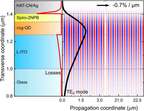
A device architecture that features reduced optical losses. It has the following structure: glass/L-ITO (250 nm)/ccg-QDs (95 nm)/Spiro-2NPB (50 nm)/HAT-CN (10 nm)/Ag (100 nm). A COMSOL-based photonic simulation of the spatial distribution of the intensity of the TE0 mode and the loss coefficient are shown by the black and red lines, respectively. The striped image to the right illustrates a propagation pattern of the TE0 mode. Reproduced with permission from ref (62) (CC-BY 4.0).
A device stack reported in refs (17) and (62) is depicted in Figure 41 along with cross-sectional distributions of the TE optical mode intensity (black line) and the optical-loss coefficient (red line). Due to the use of low-index L-ITO and the removal of the ZnO ETL, the optical mode exhibited improved confinement within the ccg-QD layer, which led to a high ΓNC of ∼40% (Figure 41, right). Further, the device also exhibited reduced optical losses with αloss of ∼143 cm–1. Based on the measured material gain of 750 cm–1 and the calculated ΓNC, the expected modal gain (300 cm–1) was higher than αloss, suggesting the feasibility of laser action in these devices.
Indeed, the developed devices showed strong 1S and 1P ASE under short-pulse optical excitation when they were cooled down to the liquid-nitrogen (LN) temperature (Figure 42). Further, when the devices were supplemented by the second order DFB cavity engraved into the L-ITO layer (Figure 43a), they showed lasing with a narrow line width of <1 nm (Figure 43b).17 Both ASE and lasing were quenched at room temperature, probably due to thermally activated electron–phonon scattering in the silver electrode leading to increased optical losses.247
Figure 42.
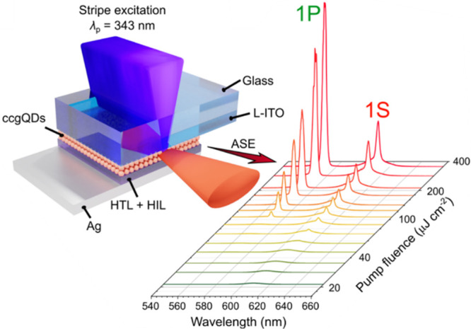
Optically excited two-band 1S and 1P ASE (right) realized using a fully stacked LED with a low-optical-loss architecture (left). The device is cooled down to the LN temperature and excited using 343 nm, 190 fs laser pulses. Reproduced with permission from ref (62) (CC-BY 4.0).
Figure 43.
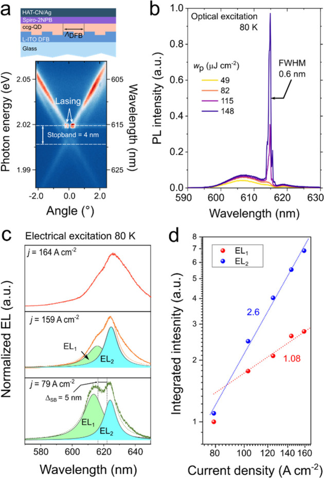
(a) An LED-like device stack with the 2nd-order DFB grating integrated into the bottom L-ITO electrode (top) and the measurements of its photonic-band structure using a Fourier-plane spectroscopy (bottom). The observed X-shaped pattern is typical of 2nd-order DFB resonators. Lasing manifests as bright spots at the shorter-wavelength edge of the photonic stopband. (b) The pump-fluence-dependent surface-emitted PL spectra of the DFB device from panel (a) exhibit the emergence of a sharp line due to DFB lasing. These data were collected at the LN temperature using excitation with 343 nm, 190 fs pulses. (c) Surface emitted EL spectra of the DFB-cavity based device measured at the LN temperature. When j is increased from 79 to 159 A cm–2, the shorter-wavelength EL feature (EL1), shifted away from the stopband of the DFB-structure, grows linearly, while the emission at the edge of the stopband (EL2) exhibits superlinear growth. This might be indicative of the onset of ASE. However, further increase in j leads to broadening and a redshift of the EL spectrum due to strong device overheating, which likely suppresses the development of laser action. (d) The EL2 intensity (IEL2) shows a superlinear growth with increasing j (IEL2 ∝ j2.6), while the growth of the EL1 feature (IEL1) is nearly linear (IEL1 ∝ j1.08). These behaviors might suggest the development of ASE due to the stopband-edge mode. Adapted with permission from ref (17) (CC-BY 4.0).
The devices presented in refs (17) and (62) also exhibited strong EL performance as high-j LEDs. At the LN temperature, their current density reached 360 A cm–2 before device breakdown. Based on the quantitative analysis of the measured EL spectra,16 the average per-dot excitonic occupancy reached ∼4. This was well above the 1S optical gain threshold and just slightly lower than the nominal 1P gain threshold.
Despite achieving population inversion with electrical pumping, the devices of refs (17) and (62) did not show either ASE or lasing under electrical excitation. The EL spectra of the DFB-cavity-based device measured at the LN temperature exhibited a pronounced stopband typical of the second-order DFB grating (Figure 43c). Furthermore, the stopband edge mode showed a superlinear intensity growth with increasing current density (Figure 43d). However, this growth did not result in the development of narrow features typical of lasing. Instead, above j of ∼160 A cm–2, the EL spectrum broadened and red-shifted indicating strong device overheating. The resulting increase in optical losses likely prevented the development of laser action. Nevertheless, the results of ref (62) were very encouraging proving the feasibility of high-j devices wherein optical gain overwhelms optical losses, the condition necessary for realizing a laser diode.
6.4. Electrically Driven ASE from Colloidal Nanocrystals
6.4.1. A Bragg Reflection Waveguide for Improved Light Amplification
Recent studies described in ref (63) achieved electrically driven ASE using room-temperature nanocrystal-based EL devices. A key feature of these prototype “mirror-less” laser diodes is an integrated Bragg reflection waveguide (BRW) formed by a bottom distributed Bragg reflector (DBR) and a top silver (Ag) electrode. The BRW approach improves optical field confinement in the nanocrystal-based active medium and simultaneously reduces mode damping in electrically conductive layers. The use of the BRW also facilitates the buildup of ASE due to the increased optical gain path length and improved light trapping within the gain medium. Below, we discuss the distinctions of the BRW devices from standard waveguiding structures based on total internal reflection (TIR).
The simplest form of a planar waveguide is a dielectric stack wherein a higher refractive index slab is sandwiched between lower-index cladding layers (Figure 44a). In this structure, light is trapped due to a TIR effect, which captures optical rays whose angle of incidence onto the slab surface satisfies condition θ > θc, where θc is the critical TIR angle defined by
| 14 |
where nwg is the refractive index of the waveguiding slab and nclad is the greater of the indices of the two cladding layers. The TIR waveguide allows for low loss propagation of optical fields with modal angles (θm) that satisfy the condition θc ≤ θm ≤ 90°.
Figure 44.
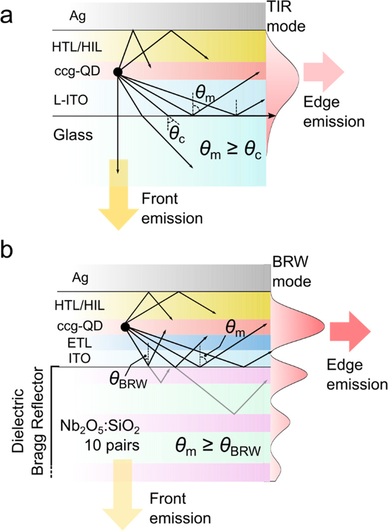
(a) A schematic illustration of light propagation in a waveguide comprising glass/L-ITO/ccg-QDs/HTL/HIL/Ag. The structure of this waveguide is similar to that of a standard LED. Low-loss light propagation occurs in the TIR regime, which is supported for optical modes whose modal angle satisfies the condition θm > θc. The critical TIR angle θc is controlled by the refractive index contrast at the L-ITO/glass interface (sin θc = nglass/nL-ITO). The intensity profile of the TIR mode is highlighted by red shading. (b) A schematic depiction of the BRW device whose structure is similar to that of the device in panel "a" except for the underlying substrate, which is not a glass slab but a DBR stack made of 10 Nb2O5/SiO2 bilayers. In the BRW device, the modal angle (θm = θBRW) is defined by the condition of constructive interference of reflections occurring within the DBR stack. As a result, the optical field profile (highlighted by red shading) exhibits an oscillatory pattern linked to the periodic structure of the DBR. Reproduced with permission from ref (63) (CC-BY 4.0).
In a BRW approach, a waveguiding slab is flanked with two reflectors, and at least one of them is a DBR (Figure 44b).286,287 A resulting structure can be thought of as a plane defect in a 1D photonic crystal. In addition to ordinary TIR modes, the BRW supports low loss propagating modes located within the DBR photonic stopband.288 They develop as a result of interference of multiple reflections that occur within the DBR stack (Figure 44b).
In the case of light amplification, BRWs offer several advantages over the TIR waveguides including improved mode confinement in an optical gain layer, reduced optical losses, and the enhanced amplification length.289,290 The latter occurs due to the increased modal angle (θBRW), which can be considerably sharper than the critical TIR angle. θBRW can be found from
| 15 |
where neff is the effective refractive index of the BRW mode, which is typically lower than nwg and can be even less than 1.286,289,290 This makes the BRW structures ideally suited for guiding light in low-index materials including gaseous media.291
6.4.2. ASE-Type LEDs with an Integrated BRW
In ref (63), the BRW was implemented by inserting a DBR comprising 10 Nb2O5/SiO2 bilayers underneath an ITO contact (Figure 45a, left). The role of the opposite reflector was played by a top Ag contact. The devices employed ∼3 monolayers of ccg-QDs as an optical gain layer. The hole-injection part was similar to that discussed in Section 6.3.2 and, in particular, it employed a low-optical-loss TFB/HAT-CN combination as an HTL/HIL (“TFB” stands for poly[(9,9-dioctylfluorenyl-2,7-diyl)-alt(4,4′-(N-(4-butylphenyl)))]).63 The electron-injection part comprised an ITO electrode followed by a ZnO ETL. Without an underlying DBR, the use of these high-index materials would lead to the unwanted shift of the peak of the optical mode away from the QD layer.272 However, this is a lesser problem in BRW structures as the optical-field distribution in a device stack is controlled primarily by the parameters of the underlying DBR.
Figure 45.
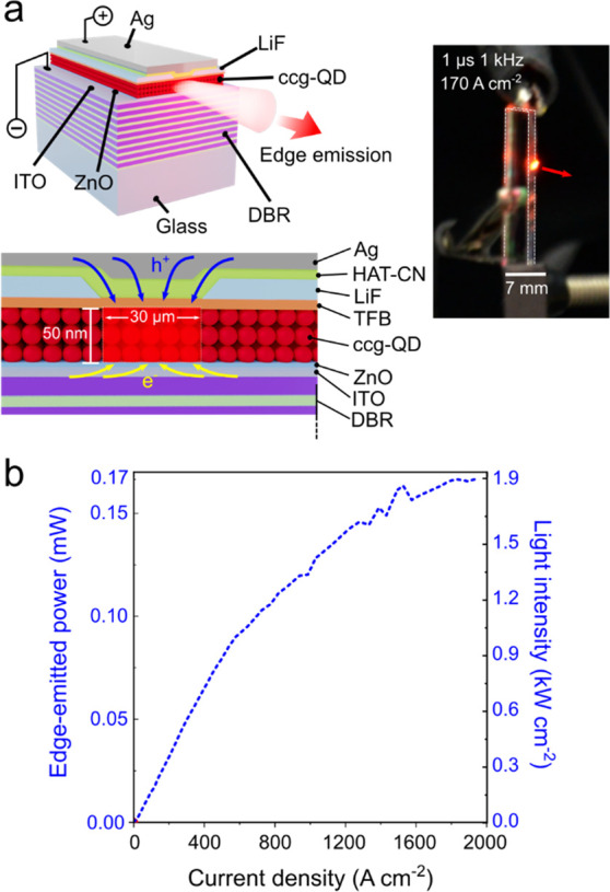
(a) A nanocrystal ASE-type LED that features a BRW formed by an underlying DBR (made of 10 Nb2O5/SiO2 bilayers) and a top silver electrode (top left). The charge injection architecture (bottom left) features 2D current focusing achieved by combining a narrow slit in a LiF interlayer and an orthogonal strip-like top contact. The device employs a TFB/HAT-CN combination as an HTL/HIL and a ZnO ETL. The active layer is made of 3 monolayers of CdSe/Cd1–xZnxSe/ZnSe0.5S0.5/ZnS ccg-QDs (Figure 40a). As depicted in the photograph on the right, the device exhibits bright edge emission clearly visible in daylight. (b) The instantaneous power of edge emission (left axis) and the estimated light intensity (right axis) of the BRW device as a function of j. At the highest j, the emitted power reaches 0.17 mW, which corresponds to the light intensity of 1.9 kW cm–2. Reproduced with permission from ref (63) (CC-BY 4.0).
Photonic modeling of these devices indicates that a major peak in the cross-sectional profile of the BRW mode is centered within the optical gain layer (Figure 44b), which leads to a high ΓNC of 23%.63 Given that the 1S material gain of the ccg-QDs is 780 cm–1 (Figure 40b), the modal gain is ∼180 cm–1. Importantly, the developed structure also exhibits a very low optical-loss coefficient of ∼16 cm–1, so it is expected to produce a high net optical gain of ∼164 cm–1. This makes it a promising candidate for realizing electrically excited laser action.
To achieve high current densities required for optical gain, the BRW structures of ref (63) employed 2D current focusing (30 μm × 300 μm) realized using a narrow slit in a dielectric LiF interlayer in combination with an orthogonal strip-shaped Ag electrode. The edge-emitting area was defined by the width of the current-focusing slit (30 μm) and the overall device thickness (300 nm). The device was excited using 1 μs electrical pulses with a pulse-to-pulse period of 1 ms.
Despite a very small size of the emitting spot and a small duty cycle of 0.1%, the device produced bright edge emission visible in daylight (Figure 45a, right). The instantaneous power reached 170 μW at j = 1933 A cm–2 (Figure 45b). The high intensity of edge emitted light provided a strong indication that the device operated in the regime that was distinct from that of standard LEDs that are not edge- but surface-emitting structures. The reason for this distinction was the realization of ASE that led to the buildup of optical modes propagating along the ccg-QD gain medium and emitted from device edges.
Strong evidence for ASE was provided by j-dependent EL spectra (Figure 46a). At low current densities, the device radiated weak spontaneous emission at 1.98 eV with a large line width of 82 meV (defined as a full width at half-maximum, FWHM). When j exceeded 13 A cm–2, two narrow peaks (FWHM of ∼40 meV) emerged in the EL spectra. Their spectral positions (1.93 and 2.11 eV) were consistent with those of the 1S and 1P ASE features observed for optically excited ccg-QD films. Further, their j-dependent intensity revealed a distinctive superlinear growth above threshold current density jth,ASE = 13 A cm–2 (Figure 46b, top), which was accompanied by the narrowing of the band-edge EL feature (Figure 46b, bottom). All of these observations pointed toward ASE character of radiated light.
Figure 46.
(a) Current-density-dependent spectra of edge-emitted EL of the BRW device (Figure 45a) exhibit the transition from broad-band spontaneous emission (green line) to ASE (blue, red, and black lines), which manifests as two sharp peaks at the positions of the 1S and 1P transitions. (b) Intensities of the 1S spontaneous emission (black) and ASE (red) EL bands as a function of current density (top) and the dependence of the 1S emission FWHM on j (bottom). These data indicate the ASE threshold of 13 A cm–2, after which the ASE peak shows accelerated growth accompanied by line narrowing. (c) Polarization characteristics of edge-emitted EL of the BRW device measured at j = 650 A cm–2. The broader spontaneous-emission band at 1.98 eV does not exhibit preferred polarization. In contrast, the narrower 1S (1.93 eV) and 1P (2.11 eV) peaks are TE polarized. This type of polarization is expected for ASE as its development requires low-loss light propagation in a waveguided which is not possible for strongly damped TM modes. Indeed, neither of the sharp peaks is present in the TM polarized EL spectrum. Reproduced with permission from ref (63) (CC-BY 4.0).
The ASE regime was also indicated by polarization characteristics of edge-emitted light. Both 1S and 1P ASE peaks were TE-polarized while the spontaneous emission band did not exhibit preferred polarization (Figure 46c).20 This difference in polarization behaviors is an anticipated effect of ASE which develops as a result of light propagation in the gain medium. Due to strong quenching of the propagating TM modes by the metal electrode (Section 6.2.2, Figure 38), the process of amplification preferentially develops for the TE modes.
Based on the characterization of multiple devices, the average ASE threshold was ∼30 A cm–2 and the standard deviation was ∼50%.63 Large variability in jth,ASE was ascribed to high sensitivity of the ASE threshold to device-to-device variations in propagation losses and a varied degree of charging of an active QD layer. In particular, as discussed in ref (63), lower values of jth,ASE may arise due to a higher degree of QD charging with extra electrons which commonly occurs in LEDs with a ZnO ETL.
The studies of ref (63) yielded a long-desired demonstration of ASE with electrically excited colloidal nanocrystals. Importantly, an entire device stack was assembled on an inexpensive commercial DBR/ITO substrate using spin coating procedures supplemented by standard thermal evaporation, and none of the fabrication step required a clean-room environment. The demonstrated ASE devices are of immediate practical utility in, for example, displays, lighting, metrology, and sensing as sources of intense, broadband, fairly directional light with considerable spatial coherence.63 They can also be explored as a platform for implementing on-chip optical amplifiers and ASE light sources that can be readily integrated with electronic and photonic circuits via standard solution-based processing techniques.
The next milestone in the area of nanocrystal-based electrically pumped light amplification devices is the realization of a laser oscillator or a “true” laser diode. This can be accomplished by, for example, supplementing an architecture of ASE devices of ref (63) with an optical resonator for circulating light through an optical gain medium. One challenge in this task is that the resonator should be implemented in such a way as to not interfere with charge injection pathways. Furthermore, it must be designed so as a circulating optical field does not experience considerable losses in the presence of charge conducting layers needed for EL operation.
As demonstrated previously, the above conditions can be satisfied with a planar DFB resonator.15,17,28,272 In particular, the DFB cavity can be readily incorporated into an EL device by simply patterning one of the existing layers of the device stack. Further, the cavity resonance can be easily tuned by varying the grating period without modifying a device cross-sectional structure, and thus without a considerable effect on charge injection. In addition, a DFB cavity can produce high “single-pass” gain even with a thin optical-gain medium (as required for efficient charge injection) as light amplification occurs in a lateral direction, and hence the corresponding propagation length is not limited by the thickness of an active layer. The lateral character of light circulation in the DFB cavity also reduces interference from adjacent charge transport layers and thereby helps reduce optical losses.
Due to these reasons, DFB resonators have been widely used in research into electrically pumped lasers based on organic materials27,28 and, recently, have been also successfully applied in devices based on colloidal nanocrystals.17,272 Future efforts on the realization of DFB-type nanocrystal laser diodes can, in principle, take advantage of a BRW architecture demonstrated in ref (63). In particular, by using a BRW in a DFB device one can achieve accurate control of a cross-sectional optical-field profile and enhance a mode confinement factor for a nanocrystal layer and simultaneously reduce field intensity in optically lossy charge conducting layers. This would increase the net optical gain coefficient and as a result would simplify the realization of laser action.
7. Summary and Outlook
It has been 30 years since the first demonstration of the lasing effect with semiconductor nanocrystals embedded in glass matrices52—the samples akin to standard colored glass filters. This demonstration opened the door for new lasing technologies based on 0D materials whose benefits as optical gain media were previously established by theoretical works.37,292 Following this discovery, it took three years to realize lasing with a different class of 0D systems—epitaxial quantum QDs grown via vacuum-based layer-by-layer deposition.293 Presently, epitaxial QD lasers are mature devices that demonstrate extra-low lasing thresholds269 and unprecedented temperature stability.294
The progress in the area of chemically synthesized nanocrystals, or colloidal QDs, was slowed by unexpected hindrance arising from nonradiative Auger recombination.89,102 This effect has a minor influence in bulk wide-gap semiconductors because of the band gap-dependent thermal activation factor, which scales as exp(−aEg/kBT);92 here a is a band-structure-dependent constant. However, due to relaxation of momentum conservation, this factor does not influence Auger rates in ultrasmall 0D nanocrystals.295 As a result, Auger decay becomes a dominant recombination channel for multicarrier states (e.g., biexcitons) leading to very fast optical gain relaxation.
The impact of Auger effects on optical gain in nanocrystals became understood only in the late-1990s to 2000s.29,54 Shortly after that, ASE was demonstrated using dense solid-state QD films pumped by short femtosecond pulses, which were the measures required to overcome fast Auger relaxation of optical gain.29 These breakthrough experiments instigated a flurry of subsequent studies. These works have produced a tremendous amount of exciting science, however, without considerable success on the front of technologically viable applications. As in the early days of nanocrystal lasing research, the primary hindrance was very fast optical gain relaxation due to Auger decay.54 This greatly complicates the realization of optically pumped cw lasers and electrically pumped laser diodes, which are the devices of primary interest from the technological standpoint.
Several recent advances have boosted the potential of colloidal nanocrystals as practically applicable optical gain media. Many of them have stemmed from the development of QDs with suppressed Auger recombination such as thick-shell “giant” CdSe/CdS QDs139,296 and compositionally graded nanostructures such as CdSe/Cd1–xZnxSe QDs.59,61 Their use has enabled several important breakthroughs including the demonstration of cw nanocrystal lasers,60 the realization of optical gain with electrical pumping,59 and the development of proof-of-principle electrically driven ASE light sources based on colloidal nanocrystals.63
Several future developments can be envisioned for this area. One could be the achievement of optically excited lasing with incoherent pump sources such as commercial high-power LEDs. In the area of laser diodes, the next important step would be the demonstration of laser oscillators in devices supplemented by an optical cavity following, for example, the recipes of refs (62) and (272). When realized, such devices will be of great utility in integrated microelectronics and photonics31 and, in particular, they will allow for implementation of lasers and amplifies assembled directly on a silicon chip.273,297−300
As previously, colloidal nanocrystals continue to serve as a highly versatile testbed for trying novel optical gain and lasing concepts. Very promising are the ideas of charged-exciton gain first introduced in ref (118) and utilized most recently to demonstrate the viability of zero-threshold optical gain119 and low-threshold subsingle-exciton lasing.61 The newest development in this area is the realization of IR-emitting nanocrystal lasers based on n-doped PbS QDs.123,284
Interesting opportunities are associated with a recently discovered Auger-assisted optical gain that relies on the process of stimulated emission accompanied by Auger-type intraband re-excitation of a colocated carrier. This process allows one to generate broad-band gain in the absorption-free sub-bandgap region, which can be explored in the context of low-noise amplification of weak signals. This gain mechanism can also enable multicolor lasing by exploiting it together with traditional optical gain processes due to inversion of band-edge and higher-lying QD transitions.
This overview of recent progress in nanocrystal lasing reaffirms great potential of these highly versatile materials in future lasing technologies. Their role can be especially significant in areas that would benefit from the ease of their manipulation via solution-based methods without constrains existing in the case of traditional epitaxial materials. These include the areas of integrated photonics and electronics, fiber optics, optical interconnects, wearable devices, and many others.
Acknowledgments
Many advances overviewed in this review have been instigated by research of past and present members of the Nanotechnology and Advanced Spectroscopy Team in the Chemistry Division of Los Alamos National Laboratory (LANL). We are especially thankful to Young-Shin Park, Jaehoon Lim, Wan Ki Bae, Heeyoung Jung, Kaifeng Wu, Jun Du, Jeongkyun Roh, Oleg Kozlov, Igor Fedin, Ho Jin, Donghyo Hahm, and Vladimir Sayevich. V.I.K. and C.L. acknowledge support by the Laboratory Directed Research and Development (LDRD) program at Los Alamos National Laboratory under project 20230352ER. N.A. and V.P. were supported by the LANL Director’s Postdoctoral Fellowship Program.
Biographies
Namyoung Ahn is a Director’s Postdoctoral Fellow in the Chemistry Division of Los Alamos National Laboratory (LANL). He obtained his B.S. (2013) and Ph.D. (2018) degrees in Mechanical and Aerospace Engineering from Seoul National University. From 2018 to 2020, he conducted postdoctoral research at Global Frontier Center for Multiscale Energy Systems in South Korea. The focus of his present studies at LANL is on fundamental and applied aspects of colloidal nanocrystal LEDs, lasers, and optical amplifiers.
Clément Livache is a Postdoctoral Research Associate in the Chemistry Division of LANL. He received an engineering degree in Chemistry from Chimie Paris Tech, as well as a M.S. degree in Solid State Physics from Sorbonne University, Paris, in 2016. He conducted his Ph.D. studies at Sorbonne University, where he worked on narrow-gap colloidal nanocrystals for infrared imaging. His current research focuses on photophysics of colloidal nanomaterials for lasing and energy applications.
Valerio Pinchetti is a Director’s Postdoctoral Fellow in the Chemistry Division of LANL. He received his M.S. (2013) and Ph.D. (2018) degrees from the University of Milano Bicocca, where he worked on advanced spectroscopy of II-VI, I-III-VI, and perovskite nanocrystals with a focus on the dopant-to-exciton magnetic interactions. His research at LANL focuses on magneto-optics and photophysics of colloidal nanomaterials.
Victor I. Klimov is a LANL Fellow and Leader of the Nanotechnology and Advanced Spectroscopy Team in the Chemistry Division of LANL. He received his M.S. (1978), Ph.D. (1981), and D.Sc. (1993) degrees from Moscow State University, Russia. His research interests include photophysics of semiconductor nanocrystals, and fundamental and applied aspects of colloidal QD lasers, light-emitting diodes, photovoltaics, and luminescent solar concentrators.
Author Contributions
† N.A. and C.L. contributed equally to this paper. CRediT:Namyoung Ahn investigation, methodology, writing-original draft; Clément Livache investigation, methodology, writing-original draft; Valerio Pinchetti investigation, methodology, writing-original draft; Victor I. Klimov conceptualization, methodology, project administration, resources, supervision, writing-original draft, writing-review & editing.
The authors declare no competing financial interest.
Special Issue
Published as part of the Chemical Reviewsvirtual special issue “Emerging Materials for Optoelectronics”.
References
- Liao P. F.; Kelley P.. Quantum Well Lasers; Elsevier, 2012. [Google Scholar]
- Nakamura S.; Senoh M.; Nagahama S.-i.; Iwasa N.; Yamada T.; Matsushita T.; Hiroyuki Kiyoku H. K.; Yasunobu Sugimoto Y. S. InGaN-Based Multi-Quantum-Well-Structure Laser Diodes. Jpn. J. Appl. Phys. 1996, 35, L74. 10.1143/JJAP.35.L74. [DOI] [Google Scholar]
- Bour D. P.AlGaInP Quantum Well Lasers. In Quantum Well Lasers; Academic Press, 1993; pp 415–453. [Google Scholar]
- Choi H. K.; Wang C. A. InGaAs/AlGaAs Strained Single Quantum Well Diode Lasers with Extremely Low Threshold Current Density and High Efficiency. Appl. Phys. Lett. 1990, 57, 321–323. 10.1063/1.103678. [DOI] [Google Scholar]
- Choi H. K.; Eglash S. J. High-Power Multiple-Quantum-Well GaInAsSb/AlGaAsSb Diode Lasers Emitting at 2.1 μm with Low Threshold Current Density. Appl. Phys. Lett. 1992, 61, 1154–1156. 10.1063/1.107630. [DOI] [Google Scholar]
- Tarasov I. S.; Pikhtin N. A.; Slipchenko S. O.; Sokolova Z. N.; Vinokurov D. A.; Borschev K. S.; Kapitonov V. A.; Khomylev M. A.; Leshko A. Y.; Lyutetskiy A. V.; et al. High Power CW (16W) and Pulse (145W) Laser Diodes Based on Quantum Well Heterostructures. Spectrochim. Acta A Mol. Biomol. Spectrosc. 2007, 66, 819–823. 10.1016/j.saa.2006.10.051. [DOI] [PubMed] [Google Scholar]
- Yoshida H.; Yamashita Y.; Kuwabara M.; Kan H. A 342-nm Ultraviolet AlGaN Multiple-Quantum-Well Laser Diode. Nat. Photonics 2008, 2, 551–554. 10.1038/nphoton.2008.135. [DOI] [Google Scholar]
- Mead C.; Conway L.. Introduction to VLSI Systems; Addison-Wesley: Reading, MA, 1980. [Google Scholar]
- Krishnamoorthy A. V.; Goossen K. W. Optoelectronic-VLSI: Photonics Integrated with VLSI Circuits. IEEE J. Sel. Top. Quantum Electron. 1998, 4, 899–912. 10.1109/2944.736073. [DOI] [Google Scholar]
- Orieux A.; Diamanti E. Recent Advances on Integrated Quantum Communications. J. Opt. 2016, 18, 083002. 10.1088/2040-8978/18/8/083002. [DOI] [Google Scholar]
- Roelkens G.; Van Campenhout J.; Brouckaert J.; Van Thourhout D.; Baets R.; Romeo P. R.; Regreny P.; Kazmierczak A.; Seassal C.; Letartre X.; et al. III-V/Si Photonics by Die-to-Wafer Bonding. Mater. Today 2007, 10, 36–43. 10.1016/S1369-7021(07)70178-5. [DOI] [Google Scholar]
- Balslev S.; Jorgensen A. M.; Bilenberg B.; Mogensen K. B.; Snakenborg D.; Geschke O.; Kutter J. P.; Kristensen A. Lab-on-a-Chip with Integrated Optical Transducers. Lab Chip 2006, 6, 213–217. 10.1039/B512546D. [DOI] [PubMed] [Google Scholar]
- Higurashi E.; Sawada R.; Ito T. An Integrated Laser Blood Flowmeter. J. Light. Technol. 2003, 21, 591. 10.1109/JLT.2003.809551. [DOI] [Google Scholar]
- Vannahme C.; Klinkhammer S.; Lemmer U.; Mappes T. Plastic Lab-on-a-Chip for Fluorescence Excitation with Integrated Organic Semiconductor Lasers. Opt. Express 2011, 19, 8179–8186. 10.1364/OE.19.008179. [DOI] [PubMed] [Google Scholar]
- Jung H.; Ahn N.; Klimov V. I. Prospects and Challenges of Colloidal Quantum Dot Laser Diodes. Nat. Photonics 2021, 15, 643–655. 10.1038/s41566-021-00827-6. [DOI] [Google Scholar]
- Jung H.; Park Y.-S.; Ahn N.; Lim J.; Fedin I.; Livache C.; Klimov V. I. Two-Band Optical Gain and Ultrabright Electroluminescence from Colloidal Quantum Dots at 1000 A cm–2. Nat. Commun. 2022, 13, 3734. 10.1038/s41467-022-31189-4. [DOI] [PMC free article] [PubMed] [Google Scholar]
- Ahn N.; Park Y.-S.; Livache C.; Du J.; Gungor K.; Kim J.; Klimov V. I. Optically Excited Lasing in a Cavity-Based, High-Current-Density Quantum Dot Electroluminescent Device. Adv. Mater. 2023, 35, 2206613. 10.1002/adma.202206613. [DOI] [PubMed] [Google Scholar]
- Du J.; Singh R.; Fedin I.; Fuhr A. S.; Klimov V. I. Spectroscopic Insights into High Defect Tolerance of Zn:CuInSe2 Quantum-Dot-Sensitized Solar Cells. Nat. Energy 2020, 5, 409–417. 10.1038/s41560-020-0617-6. [DOI] [Google Scholar]
- Wu K.; Li H.; Klimov V. I. Tandem Luminescent Solar Concentrators Based on Engineered Quantum Dots. Nat. Photonics 2018, 12, 105–110. 10.1038/s41566-017-0070-7. [DOI] [Google Scholar]
- Kozlov V. G.; Bulović V.; Burrows P. E.; Forrest S. R. Laser Action in Organic Semiconductor Waveguide and Double-Heterostructure Devices. Nature 1997, 389, 362–364. 10.1038/38693. [DOI] [Google Scholar]
- Eaton S. W.; Fu A.; Wong A. B.; Ning C.-Z.; Yang P. Semiconductor Nanowire Lasers. Nat. Rev. Mater. 2016, 1, 16028. 10.1038/natrevmats.2016.28. [DOI] [Google Scholar]
- Saliba M.; Wood S. M.; Patel J. B.; Nayak P. K.; Huang J.; Alexander-Webber J. A.; Wenger B.; Stranks S. D.; Horantner M. T.; Wang J. T.-W.; Nicholas R. J.; Herz L. M.; Johnston M. B.; Morris S. M.; Snaith H. J.; Riede M. K. Structured Organic-Inorganic Perovskite toward a Distributed Feedback Laser. Adv. Mater. 2016, 28, 923–929. 10.1002/adma.201502608. [DOI] [PubMed] [Google Scholar]
- Chen S.; Roh K.; Lee J.; Chong W. K.; Lu Y.; Mathews N.; Sum T. C.; Nurmikko A. A Photonic Crystal Laser from Solution Based Organo-Lead Iodide Perovskite Thin Films. ACS Nano 2016, 10, 3959–3967. 10.1021/acsnano.5b08153. [DOI] [PubMed] [Google Scholar]
- Yakunin S.; Protesescu L.; Krieg F.; Bodnarchuk M. I.; Nedelcu G.; Humer M.; De Luca G.; Fiebig M.; Heiss W.; Kovalenko M. V. Low-Threshold Amplified Spontaneous Emission and Lasing from Colloidal Nanocrystals of Caesium Lead Halide Perovskites. Nat. Commun. 2015, 6, 8056. 10.1038/ncomms9056. [DOI] [PMC free article] [PubMed] [Google Scholar]
- Wang Y.; Li X.; Nalla V.; Zeng H.; Sun H. Solution-Processed Low Threshold Vertical Cavity Surface Emitting Lasers from All-Inorganic Perovskite Nanocrystals. Adv. Funct. Mater. 2017, 27, 1605088. 10.1002/adfm.201605088. [DOI] [Google Scholar]
- Sandanayaka A. S. D.; Yoshida K.; Inoue M.; Qin C.; Goushi K.; Ribierre J.-C.; Matsushima T.; Adachi C. Quasi-Continuous-Wave Organic Thin-Film Distributed Feedback Laser. Adv. Opt. Mater. 2016, 4, 834–839. 10.1002/adom.201600006. [DOI] [Google Scholar]
- Sandanayaka A. S. D.; Matsushima T.; Bencheikh F.; Yoshida K.; Inoue M.; Fujihara T.; Goushi K.; Ribierre J.-C.; Adachi C. Toward Continuous-Wave Operation of Organic Semiconductor Lasers. Sci. Adv. 2017, 3, e1602570 10.1126/sciadv.1602570. [DOI] [PMC free article] [PubMed] [Google Scholar]
- Sandanayaka A. S. D.; Matsushima T.; Bencheikh F.; Terakawa S.; Potscavage W. J.; Qin C.; Fujihara T.; Goushi K.; Ribierre J.-C.; Adachi C. Indication of Current-Injection Lasing from an Organic Semiconductor. Appl. Phys. Express 2019, 12, 061010. 10.7567/1882-0786/ab1b90. [DOI] [Google Scholar]
- Klimov V. I.; Mikhailovsky A. A.; Xu S.; Malko A.; Hollingsworth J. A.; Leatherdale C. A.; Eisler H. J.; Bawendi M. G. Optical Gain and Stimulated Emission in Nanocrystal Quantum Dots. Science 2000, 290, 314–317. 10.1126/science.290.5490.314. [DOI] [PubMed] [Google Scholar]
- Wang Y.; Sun H. Advances and Prospects of Lasers Developed from Colloidal Semiconductor Nanostructures. Prog. Quantum Electron. 2018, 60, 1–29. 10.1016/j.pquantelec.2018.05.002. [DOI] [Google Scholar]
- Geiregat P.; Van Thourhout D.; Hens Z. A Bright Future for Colloidal Quantum Dot Lasers. NPG Asia Mater. 2019, 11, 41. 10.1038/s41427-019-0141-y. [DOI] [Google Scholar]
- Park Y.-S.; Roh J.; Diroll B. T.; Schaller R. D.; Klimov V. I. Colloidal Quantum Dot Lasers. Nat. Rev. Mater. 2021, 6, 382–401. 10.1038/s41578-020-00274-9. [DOI] [Google Scholar]
- Kwak J.; Lim J.; Park M.; Lee S.; Char K.; Lee C. High-Power Genuine Ultraviolet Light-Emitting Diodes Based On Colloidal Nanocrystal Quantum Dots. Nano Lett. 2015, 15, 3793–3799. 10.1021/acs.nanolett.5b00392. [DOI] [PubMed] [Google Scholar]
- Kwak J.; Bae W. K.; Lee D.; Park I.; Lim J.; Park M.; Cho H.; Woo H.; Yoon D. Y.; Char K.; et al. Bright and Efficient Full-Color Colloidal Quantum Dot Light-Emitting Diodes Using an Inverted Device Structure. Nano Lett. 2012, 12, 2362–2366. 10.1021/nl3003254. [DOI] [PubMed] [Google Scholar]
- Pradhan S.; Dalmases M.; Taghipour N.; Kundu B.; Konstantatos G. Colloidal Quantum Dot Light Emitting Diodes at Telecom Wavelength with 18% Quantum Efficiency and Over 1 MHz Bandwidth. Adv. Sci. 2022, 9, 2200637. 10.1002/advs.202200637. [DOI] [PMC free article] [PubMed] [Google Scholar]
- Minotto A.; Bulut I.; Rapidis A. G.; Carnicella G.; Patrini M.; Lunedei E.; Anderson H. L.; Cacialli F. Towards Efficient Near-Infrared Fluorescent Organic Light-Emitting Diodes. Light: Science Applications 2021, 10, 18. 10.1038/s41377-020-00456-8. [DOI] [PMC free article] [PubMed] [Google Scholar]
- Arakawa Y.; Sakaki H. Multidimensional Quantum Well Laser and Temperature-Dependence of Its Threshold Current. Appl. Phys. Lett. 1982, 40, 939–941. 10.1063/1.92959. [DOI] [Google Scholar]
- Alivisatos A. P. Semiconductor Clusters, Nanocrystals, and Quantum Dots. Science 1996, 271, 933–937. 10.1126/science.271.5251.933. [DOI] [Google Scholar]
- Pietryga J. M.; Park Y.-S.; Lim J.; Fidler A. F.; Bae W. K.; Brovelli S.; Klimov V. I. Spectroscopic and Device Aspects of Nanocrystal Quantum Dots. Chem. Rev. 2016, 116, 10513–10622. 10.1021/acs.chemrev.6b00169. [DOI] [PubMed] [Google Scholar]
- Tao A. R.; Habas S.; Yang P. Shape Control of Colloidal Metal Nanocrystals. Small 2008, 4, 310–325. 10.1002/smll.200701295. [DOI] [Google Scholar]
- Sayevich V.; Robinson Z. L.; Kim Y.; Kozlov O. V.; Jung H.; Nakotte T.; Park Y.-S.; Klimov V. I. Highly Versatile Near-Infrared Emitters Based on an Atomically Defined HgS Interlayer Embedded into a CdSe/CdS Quantum Dot. Nat. Nanotechnol. 2021, 16, 673–679. 10.1038/s41565-021-00871-x. [DOI] [PubMed] [Google Scholar]
- Murray C. B.; Norris D. J.; Bawendi M. G. Synthesis and Characterization of Nearly Monodisperse CdE (E = Sulfur, Selenium, Tellurium) Semiconductor Nanocrystallites. J. Am. Chem. Soc. 1993, 115, 8706–8715. 10.1021/ja00072a025. [DOI] [Google Scholar]
- Pietryga J. M.; Hollingsworth J. A.; Kilmov V. I.; Schaller R. D.; Stewart M. H.; Nanda J. Pushing the Band Gap Envelope: PbSe Quantum Dots Emitting at 3 Microns and Beyond. Abstr. Pap. Am. Chem. Soc. 2004, 227, U1552–U1552. [DOI] [PubMed] [Google Scholar]
- Protesescu L.; Yakunin S.; Bodnarchuk M. I.; Krieg F.; Caputo R.; Hendon C. H.; Yang R. X.; Walsh A.; Kovalenko M. V. Nanocrystals of Cesium Lead Halide Perovskites (CsPbX3, X = Cl, Br, and I): Novel Optoelectronic Materials Showing Bright Emission with Wide Color Gamut. Nano Lett. 2015, 15, 3692–3696. 10.1021/nl5048779. [DOI] [PMC free article] [PubMed] [Google Scholar]
- Peng X. G.; Manna L.; Yang W. D.; Wickham J.; Scher E.; Kadavanich A.; Alivisatos A. P. Shape Control of CdSe Nanocrystals. Nature 2000, 404, 59–61. 10.1038/35003535. [DOI] [PubMed] [Google Scholar]
- Son J. S.; Yu J. H.; Kwon S. G.; Lee J.; Joo J.; Hyeon T. Colloidal Synthesis of Ultrathin Two-Dimensional Semiconductor Nanocrystals. Adv. Mater. 2011, 23, 3214–3219. 10.1002/adma.201101334. [DOI] [PubMed] [Google Scholar]
- Ithurria S.; Tessier M. D.; Mahler B.; Lobo R. P. S. M.; Dubertret B.; Efros A. L. Colloidal Nanoplatelets with Two-Dimensional Electronic Structure. Nat. Mater. 2011, 10, 936–941. 10.1038/nmat3145. [DOI] [PubMed] [Google Scholar]
- Manna L.; Scher E. C.; Alivisatos A. P. Synthesis of Soluble and Processable Rod-, Arrow-, Teardrop-, and Tetrapod-Shaped CdSe Nanocrystals. J. Am. Chem. Soc. 2000, 122, 12700–12706. 10.1021/ja003055+. [DOI] [Google Scholar]
- Kholmicheva N.; Budkina D. S.; Cassidy J.; Porotnikov D.; Harankahage D.; Boddy A.; Galindo M.; Khon D.; Tarnovsky A. N.; Zamkov M. Sustained Biexciton Populations in Nanoshell Quantum Dots. ACS Photonics 2019, 6, 1041–1050. 10.1021/acsphotonics.9b00068. [DOI] [Google Scholar]
- Cassidy J.; Zamkov M. Nanoshell Quantum Dots: Quantum Confinement Beyond the Exciton Bohr Radius. J. Chem. Phys. 2020, 152, 110902. 10.1063/1.5126423. [DOI] [PubMed] [Google Scholar]
- Jeong B. G.; Park Y.-S.; Chang J. H.; Cho I.; Kim J. K.; Kim H.; Char K.; Cho J.; Klimov V. I.; Park P.; et al. Colloidal Spherical Quantum Wells with Near-Unity Photoluminescence Quantum Yield and Suppressed Blinking. ACS Nano 2016, 10, 9297–9305. 10.1021/acsnano.6b03704. [DOI] [PubMed] [Google Scholar]
- Vandyshev Y. V.; Dneprovskii V. S.; Klimov V. I.; Okorokov D. K. Lasing on a Transition between Quantum-Well Levels in a Quantum Dot. J. Exp. Theor. Phys. Lett. 1991, 54, 442–445. [Google Scholar]
- Ekimov A. Growth and Optical Properties of Semiconductor Nanocrystals in a Glass Matrix. J. Lumin. 1996, 70, 1–20. 10.1016/0022-2313(96)00040-3. [DOI] [Google Scholar]
- Klimov V. I.; Mikhailovsky A. A.; McBranch D. W.; Leatherdale C. A.; Bawendi M. G. Quantization of Multiparticle Auger Rates in Semiconductor Quantum Dots. Science 2000, 287, 1011–1013. 10.1126/science.287.5455.1011. [DOI] [PubMed] [Google Scholar]
- Bae W. K.; Padilha L. A.; Park Y.-S.; McDaniel H.; Robel I.; Pietryga J. M.; Klimov V. I. Controlled Alloying of the Core-Shell Interface in CdSe/CdS Quantum Dots for Suppression of Auger Recombination. ACS Nano 2013, 7, 3411–3419. 10.1021/nn4002825. [DOI] [PubMed] [Google Scholar]
- Bae W. K.; Park Y.-S.; Lim J.; Lee D.; Padilha L. A.; McDaniel H.; Robel I.; Lee C.; Pietryga J. M.; Klimov V. I. Controlling the Influence of Auger Recombination on the Performance of Quantum-Dot Light-Emitting Diodes. Nat. Commun. 2013, 4, 2661. 10.1038/ncomms3661. [DOI] [PMC free article] [PubMed] [Google Scholar]
- Park Y.-S.; Bae W. K.; Padilha L. A.; Pietryga J. M.; Klimov V. I. Effect of the Core/Shell Interface on Auger Recombination Evaluated by Single-Quantum-Dot Spectroscopy. Nano Lett. 2014, 14, 396–402. 10.1021/nl403289w. [DOI] [PubMed] [Google Scholar]
- Park Y.-S.; Lim J.; Makarov N. S.; Klimov V. I. Effect of Interfacial Alloying versus “Volume Scaling” on Auger Recombination in Compositionally Graded Semiconductor Quantum Dots. Nano Lett. 2017, 17, 5607–5613. 10.1021/acs.nanolett.7b02438. [DOI] [PubMed] [Google Scholar]
- Lim J.; Park Y.-S.; Klimov V. I. Optical Gain in Colloidal Quantum Dots Achieved with Direct-Current Electrical Pumping. Nat. Mater. 2018, 17, 42–49. 10.1038/nmat5011. [DOI] [PubMed] [Google Scholar]
- Fan F.; Voznyy O.; Sabatini R. P.; Bicanic K. T.; Adachi M. M.; McBride J. R.; Reid K. R.; Park Y.-S.; Li X.; Jain A.; et al. Continuous-Wave Lasing in Colloidal Quantum Dot Solids Enabled by Facet-Selective Epitaxy. Nature 2017, 544, 75–79. 10.1038/nature21424. [DOI] [PubMed] [Google Scholar]
- Kozlov O. V.; Park Y.-S.; Roh J.; Fedin I.; Nakotte T.; Klimov V. I. Sub-Single-Exciton Lasing Using Charged Quantum Dots Coupled to a Distributed Feedback Cavity. Science 2019, 365, 672–675. 10.1126/science.aax3489. [DOI] [PubMed] [Google Scholar]
- Ahn N.; Park Y.-S.; Livache C.; Du J.; Klimov V. I.. Optically Excited Two-Band Amplified Spontaneous Emission from a High-Current-Density Quantum-Dot LED. arXiv preprint arXiv:2204.01929 2022. 10.48550/arXiv.2204.01929 [DOI] [Google Scholar]
- Ahn N.; Livache C.; Pinchetti V.; Jung H.; Jin H.; Park Y.-S.; Hahm D.; Klimov V. I. Electrically Driven Amplified Spontaneous Emission from Colloidal Quantum Dots. Nature 2023, 617, 79. 10.1038/s41586-023-05855-6. [DOI] [PMC free article] [PubMed] [Google Scholar]
- Grivas C.; Pollnau M. Organic Solid-State Integrated Amplifiers and Lasers. Laser & Photonics Rev. 2012, 6, 419–462. 10.1002/lpor.201100034. [DOI] [Google Scholar]
- Cubukcu E.; Kort E. A.; Crozier K. B.; Capasso F. Plasmonic Laser Antenna. Appl. Phys. Lett. 2006, 89, 093120. 10.1063/1.2339286. [DOI] [Google Scholar]
- Savage N. Linking with Light [High-Speed Optical Interconnects]. IEEE Spectr. 2002, 39, 32–36. 10.1109/MSPEC.2002.1021941. [DOI] [Google Scholar]
- Vollmer F.; Arnold S. Whispering-Gallery-Mode Biosensing: Label-Free Detection Down to Single Molecules. Nat. Methods 2008, 5, 591–596. 10.1038/nmeth.1221. [DOI] [PubMed] [Google Scholar]
- Chen J.; Du W.; Shi J.; Li M.; Wang Y.; Zhang Q.; Liu X. Perovskite Quantum Dot Lasers. InfoMat 2020, 2, 170–183. 10.1002/inf2.12051. [DOI] [Google Scholar]
- Efros A. L.; Efros A. L. Interband Absorption of Light in a Semiconductor Sphere. Sov. Phys. Sem. 1982, 16, 772–775. [Google Scholar]
- Brus L. E. A Simple Model for the Ionization Potential, Electron Affinity, and Aqueous Redox Potentials of Small Semiconductor Crystallites. J. Chem. Phys. 1983, 79, 5566–5571. 10.1063/1.445676. [DOI] [Google Scholar]
- Ekimov A. I.; Hache F.; Schanne-Klein M. C.; Ricard D.; Flytzanis C.; Kudryavtsev I. A.; Yazeva T. V.; Rodina A. V.; Efros A. L. Absorption and Intensity-Dependent Photoluminescence Measurements on CdSe Quantum Dots: Assignment of the First Electronic Transitions. J. Opt. Soc. Am. B 1993, 10, 100–107. 10.1364/JOSAB.10.000100. [DOI] [Google Scholar]
- Sun L.; Choi J. J.; Stachnik D.; Bartnik A. C.; Hyun B.-R.; Malliaras G. G.; Hanrath T.; Wise F. W. Bright Infrared Quantum-Dot Light-Emitting Diodes through Inter-Dot Spacing Control. Nat. Nanotechnol. 2012, 7, 369–373. 10.1038/nnano.2012.63. [DOI] [PubMed] [Google Scholar]
- Moreels I.; Lambert K.; Smeets D.; De Muynck D.; Nollet T.; Martins J. C.; Vanhaecke F.; Vantomme A.; Delerue C.; Allan G.; et al. Size-Dependent Optical Properties of Colloidal PbS Quantum Dots. ACS Nano 2009, 3, 3023–3030. 10.1021/nn900863a. [DOI] [PubMed] [Google Scholar]
- Miller E. M.; Kroupa D. M.; Zhang J.; Schulz P.; Marshall A. R.; Kahn A.; Lany S.; Luther J. M.; Beard M. C.; Perkins C. L.; et al. Revisiting the Valence and Conduction Band Size Dependence of PbS Quantum Dot Thin Films. ACS Nano 2016, 10, 3302–3311. 10.1021/acsnano.5b06833. [DOI] [PubMed] [Google Scholar]
- Pietryga J. M.; Schaller R. D.; Werder D.; Stewart M. H.; Klimov V. I.; Hollingsworth J. A. Pushing the Band Gap Envelope: Mid-Infrared Emitting Colloidal PbSe Quantum Dots. J. Am. Chem. Soc. 2004, 126, 11752–11753. 10.1021/ja047659f. [DOI] [PubMed] [Google Scholar]
- Biadala L.; Siebers B.; Beyazit Y.; Tessier M. D.; Dupont D.; Hens Z.; Yakovlev D. R.; Bayer M. Band-Edge Exciton Fine Structure and Recombination Dynamics in InP/ZnS Colloidal Nanocrystals. ACS Nano 2016, 10, 3356–3364. 10.1021/acsnano.5b07065. [DOI] [PubMed] [Google Scholar]
- Mićić O. I.; Cheong H. M.; Fu H.; Zunger A.; Sprague J. R.; Mascarenhas A.; Nozik A. J. Size-Dependent Spectroscopy of InP Quantum Dots. J. Phys. Chem. B 1997, 101, 4904–4912. 10.1021/jp9704731. [DOI] [Google Scholar]
- Yu W. W.; Qu L.; Guo W.; Peng X. Experimental Determination of the Extinction Coefficient of CdTe, CdSe, and CdS Nanocrystals. Chem. Mater. 2003, 15, 2854–2860. 10.1021/cm034081k. [DOI] [Google Scholar]
- Yu W. W.; Wang Y. A.; Peng X. Formation and Stability of Size-, Shape-, and Structure-Controlled CdTe Nanocrystals: Ligand Effects on Monomers and Nanocrystals. Chem. Mater. 2003, 15, 4300–4308. 10.1021/cm034729t. [DOI] [Google Scholar]
- Peng X.; Wickham J.; Alivisatos A. P. Kinetics of II-VI and III-V Colloidal Semiconductor Nanocrystal Growth: “Focusing” of Size Distributions. J. Am. Chem. Soc. 1998, 120, 5343–5344. 10.1021/ja9805425. [DOI] [Google Scholar]
- Yu W. W.; Peng X. Formation of High-Quality CdS and Other II-VI Semiconductor Nanocrystals in Noncoordinating Solvents: Tunable Reactivity of Monomers. Angew. Chem., Int. Ed. 2002, 41, 2368–2371. . [DOI] [PubMed] [Google Scholar]
- Gréboval C.; Chu A.; Goubet N.; Livache C.; Ithurria S.; Lhuillier E. Mercury Chalcogenide Quantum Dots: Material Perspective for Device Integration. Chem. Rev. 2021, 121, 3627–3700. 10.1021/acs.chemrev.0c01120. [DOI] [PubMed] [Google Scholar]
- Efros A. L.; Rosen M. Quantum Size Level Structure of Narrow-Gap Semiconductor Nanocrystals: Effect of Band Coupling. Phys. Rev. B 1998, 58, 7120–7135. 10.1103/PhysRevB.58.7120. [DOI] [Google Scholar]
- Norris D. J.; Bawendi M. G. Measurement and Assignment of the Size-Dependent Optical Spectrum in CdSe Quantum Dots. Phys. Rev. B 1996, 53, 16338–16346. 10.1103/PhysRevB.53.16338. [DOI] [PubMed] [Google Scholar]
- Efros A. L.; Rosen M.; Kuno M.; Nirmal M.; Norris D. J.; Bawendi M. Band-Edge Exciton in Quantum Dots of Semiconductors with a Degenerate Valence Band: Dark and Bright Exciton States. Phys. Rev. B 1996, 54, 4843–4856. 10.1103/PhysRevB.54.4843. [DOI] [PubMed] [Google Scholar]
- Nirmal M.; Norris D. J.; Kuno M.; Bawendi M. G.; Efros A. L.; Rosen M. Observation of the Dark Excitons in CdSe Quantum Dots. Phys. Rev. Lett. 1995, 75, 3728–3731. 10.1103/PhysRevLett.75.3728. [DOI] [PubMed] [Google Scholar]
- Norris D. J.; Efros A. L.; Rosen M.; Bawendi M. G. Size Dependence of Exciton Fine Structure in CdSe Quantum Dots. Phys. Rev. B 1996, 53, 16347–16354. 10.1103/PhysRevB.53.16347. [DOI] [PubMed] [Google Scholar]
- Park Y.-S.; Bae W. K.; Baker T.; Lim J.; Klimov V. I. Effect of Auger Recombination on Lasing in Heterostructured Quantum Dots with Engineered Core/Shell Interfaces. Nano Lett. 2015, 15, 7319–7328. 10.1021/acs.nanolett.5b02595. [DOI] [PubMed] [Google Scholar]
- Klimov V. I. Optical Nonlinearities and Ultrafast Carrier Dynamics in Semiconductor Nanocrystals. J. Phys. Chem. B 2000, 104, 6112–6123. 10.1021/jp9944132. [DOI] [Google Scholar]
- Wang L.-W.; Califano M.; Zunger A.; Franceschetti A. Pseudopotential Theory of Auger Processes in CdSe Quantum Dots. Phys. Rev. Lett. 2003, 91, 056404. 10.1103/PhysRevLett.91.056404. [DOI] [PubMed] [Google Scholar]
- Efros A. L.; Rosen M. Random Telegraph Signal in the Photoluminescence Intensity of a Single Quantum Dot. Phys. Rev. Lett. 1997, 78, 1110–1113. 10.1103/PhysRevLett.78.1110. [DOI] [Google Scholar]
- Kharchenko V. A.; Rosen M. Auger Relaxation Processes in Semiconductor Nanocrystals and Quantum Wells. J. Lumin. 1996, 70, 158–169. 10.1016/0022-2313(96)00052-X. [DOI] [Google Scholar]
- Robel I.; Gresback R.; Kortshagen U.; Schaller R. D.; Klimov V. I. Universal Size-Dependent Trend in Auger Recombination in Direct-Gap and Indirect-Gap Semiconductor Nanocrystals. Phys. Rev. Lett. 2009, 102, 177404. 10.1103/PhysRevLett.102.177404. [DOI] [PubMed] [Google Scholar]
- Achermann M.; Hollingsworth J. A.; Klimov V. I. Multiexcitons Confined within a Subexcitonic Volume: Spectroscopic and Dynamical Signatures of Neutral and Charged Biexcitons in Ultrasmall Semiconductor Nanocrystals. Phys. Rev. B 2003, 68, 245302. 10.1103/PhysRevB.68.245302. [DOI] [Google Scholar]
- Fisher B.; Caruge J.-M.; Chan Y.-T.; Halpert J.; Bawendi M. G. Multiexciton Fluorescence from Semiconductor Nanocrystals. Chem. Phys. 2005, 318, 71–81. 10.1016/j.chemphys.2005.05.036. [DOI] [Google Scholar]
- Pandey A.; Guyot-Sionnest P. Multicarrier Recombination in Colloidal Quantum Dots. J. Chem. Phys. 2007, 127, 111104. 10.1063/1.2786068. [DOI] [PubMed] [Google Scholar]
- Klimov V. I.; McGuire J. A.; Schaller R. D.; Rupasov V. I. Scaling of Multiexciton Lifetimes in Semiconductor Nanocrystals. Phys. Rev. B 2008, 77, 195324. 10.1103/PhysRevB.77.195324. [DOI] [Google Scholar]
- Beard M. C.; Knutsen K. P.; Yu P.; Luther J. M.; Song Q.; Metzger W. K.; Ellingson R. J.; Nozik A. J. Multiple Exciton Generation in Colloidal Silicon Nanocrystals. Nano Lett. 2007, 7, 2506–2512. 10.1021/nl071486l. [DOI] [PubMed] [Google Scholar]
- Castañeda J. A.; Nagamine G.; Yassitepe E.; Bonato L. G.; Voznyy O.; Hoogland S.; Nogueira A. F.; Sargent E. H.; Cruz C. H. B.; Padilha L. A. Efficient Biexciton Interaction in Perovskite Quantum Dots Under Weak and Strong Confinement. ACS Nano 2016, 10, 8603–8609. 10.1021/acsnano.6b03908. [DOI] [PubMed] [Google Scholar]
- Makarov N. S.; Guo S.; Isaienko O.; Liu W.; Robel I.; Klimov V. I. Spectral and Dynamical Properties of Single Excitons, Biexcitons, and Trions in Cesium-Lead-Halide Perovskite Quantum Dots. Nano Lett. 2016, 16, 2349–2362. 10.1021/acs.nanolett.5b05077. [DOI] [PubMed] [Google Scholar]
- Rhee S.; Kim K.; Roh J.; Kwak J. Recent Progress in High-Luminance Quantum Dot Light-Emitting Diodes. Curr. Opt. Photon. 2020, 4, 161–173. [Google Scholar]
- Klimov V. I. Multicarrier Interactions in Semiconductor Nanocrystals in Relation to the Phenomena of Auger Recombination and Carrier Multiplication. Annu. Rev. Condens. Matter Phys. 2014, 5, 285–316. 10.1146/annurev-conmatphys-031113-133900. [DOI] [Google Scholar]
- Crooker S. A.; Barrick T.; Hollingsworth J. A.; Klimov V. I. Multiple Temperature Regimes of Radiative Decay in CdSe Nanocrystal Quantum Dots: Intrinsic Limits of the Dark-Exciton Lifetime. Appl. Phys. Lett. 2003, 82, 2793–2795. 10.1063/1.1570923. [DOI] [Google Scholar]
- Cragg G. E.; Efros A. L. Suppression of Auger Processes in Confined Structures. Nano Lett. 2010, 10, 313–317. 10.1021/nl903592h. [DOI] [PubMed] [Google Scholar]
- Climente J. I.; Movilla J. L.; Planelles J. Auger Recombination Suppression in Nanocrystals with Asymmetric Electron-Hole Confinement. Small 2012, 8, 754–759. 10.1002/smll.201101740. [DOI] [PubMed] [Google Scholar]
- Park Y.-S.; Lim J.; Klimov V. I. Asymmetrically Strained Quantum Dots with Non-Fluctuating Single-Dot Emission Spectra and Subthermal Room-Temperature Linewidths. Nat. Mater. 2019, 18, 249–255. 10.1038/s41563-018-0254-7. [DOI] [PubMed] [Google Scholar]
- Tomar R.; Kulkarni A.; Chen K.; Singh S.; van Thourhout D.; Hodgkiss J. M.; Siebbeles L. D. A.; Hens Z.; Geiregat P. Charge Carrier Cooling Bottleneck Opens Up Nonexcitonic Gain Mechanisms in Colloidal CdSe Quantum Wells. J. Phys. Chem. C 2019, 123, 9640–9650. 10.1021/acs.jpcc.9b02085. [DOI] [Google Scholar]
- Karel Čapek R.; Moreels I.; Lambert K.; De Muynck D.; Zhao Q.; Van Tomme A.; Vanhaecke F.; Hens Z. Optical Properties of Zincblende Cadmium Selenide Quantum Dots. J. Phys. Chem. C 2010, 114, 6371–6376. 10.1021/jp1001989. [DOI] [Google Scholar]
- Klimov V. I. Spectral and Dynamical Properties of Multiexcitons in Semiconductor Nanocrystals. Annu. Rev. Phys. Chem. 2007, 58, 635–673. 10.1146/annurev.physchem.58.032806.104537. [DOI] [PubMed] [Google Scholar]
- Shaklee K. L.; Leheny R. F. Direct Determination of Optical Gain in Semiconductor Crystals. Appl. Phys. Lett. 1971, 18, 475–477. 10.1063/1.1653501. [DOI] [Google Scholar]
- Ivanov S. A.; Nanda J.; Piryatinski A.; Achermann M.; Balet L. P.; Bezel I. V.; Anikeeva P. O.; Tretiak S.; Klimov V. I. Light Amplification Using Inverted Core/Shell Nanocrystals: Towards Lasing in the Single-Exciton Regime. J. Phys. Chem. B 2004, 108, 10625–10630. 10.1021/jp0483371. [DOI] [Google Scholar]
- Klimov V. I.; Ivanov S. A.; Nanda J.; Achermann M.; Bezel I.; McGuire J. A.; Piryatinski A. Single-Exciton Optical Gain in Semiconductor Nanocrystals. Nature 2007, 447, 441–446. 10.1038/nature05839. [DOI] [PubMed] [Google Scholar]
- Klimov V.; Hunsche S.; Kurz H. Biexciton Effects in Femtosecond Nonlinear Transmission of Semiconductor Quantum Dots. Phys. Rev. B 1994, 50, 8110–8113. 10.1103/PhysRevB.50.8110. [DOI] [PubMed] [Google Scholar]
- Piryatinski A.; Ivanov S. A.; Tretiak S.; Klimov V. I. Effect of Quantum and Dielectric Confinement on the Exciton-Exciton Interaction Energy in Type II Core/Shell Semiconductor Nanocrystals. Nano Lett. 2007, 7, 108–115. 10.1021/nl0622404. [DOI] [PubMed] [Google Scholar]
- Nanda J.; Ivanov S. A.; Achermann M.; Bezel I.; Piryatinski A.; Klimov V. I. Light Amplification in the Single-Exciton Regime Using Exciton-Exciton Repulsion in Type-II Nanocrystal Quantum Dots. J. Phys. Chem. C 2007, 111, 15382–15390. 10.1021/jp0738659. [DOI] [Google Scholar]
- Ivanov S. A.; Piryatinski A.; Nanda J.; Tretiak S.; Zavadil K. R.; Wallace W. O.; Werder D.; Klimov V. I. Type-II Core/Shell CdS/ZnSe Nanocrystals: Synthesis, Electronic Structures, and Spectroscopic Properties. J. Am. Chem. Soc. 2007, 129, 11708–11719. 10.1021/ja068351m. [DOI] [PubMed] [Google Scholar]
- Cihan A. F.; Kelestemur Y.; Guzelturk B.; Yerli O.; Kurum U.; Yaglioglu H. G.; Elmali A.; Demir H. V. Attractive versus Repulsive Excitonic Interactions of Colloidal Quantum Dots Control Blue- to Red-Shifting (and Non-shifting) Amplified Spontaneous Emission. J. Phys. Chem. Lett. 2013, 4, 4146–4152. 10.1021/jz402211m. [DOI] [Google Scholar]
- Wang C.; Wehrenberg B. L.; Woo C. Y.; Guyot-Sionnest P. Light Emission and Amplification in Charged CdSe Quantum Dots. J. Phys. Chem. B 2004, 108, 9027–9031. 10.1021/jp0489830. [DOI] [Google Scholar]
- Wu K.; Park Y.-S.; Lim J.; Klimov V. I. Towards Zero-Threshold Optical Gain Using Charged Semiconductor Quantum Dots. Nat. Nanotechnol. 2017, 12, 1140–1147. 10.1038/nnano.2017.189. [DOI] [PubMed] [Google Scholar]
- Wu K.; Lim J.; Klimov V. I. Superposition Principle in Auger Recombination of Charged and Neutral Multicarrier States in Semiconductor Quantum Dots. ACS Nano 2017, 11, 8437–8447. 10.1021/acsnano.7b04079. [DOI] [PubMed] [Google Scholar]
- Kang I.; Wise F. W. Electronic Structure and Optical Properties of PbS and PbSe Quantum Dots. J. Opt. Soc. Am. B 1997, 14, 1632–1646. 10.1364/JOSAB.14.001632. [DOI] [Google Scholar]
- Schaller R. D.; Petruska M. A.; Klimov V. I. Tunable Near-Infrared Optical Gain and Amplified Spontaneous Emission Using PbSe Nanocrystals. J. Phys. Chem. B 2003, 107, 13765–13768. 10.1021/jp0311660. [DOI] [Google Scholar]
- Whitworth G. L.; Dalmases M.; Taghipour N.; Konstantatos G. Solution-Processed PbS Quantum Dot Infrared Laser with Room-Temperature Tunable Emission in the Optical Telecommunications Window. Nat. Photonics 2021, 15, 738–742. 10.1038/s41566-021-00878-9. [DOI] [PMC free article] [PubMed] [Google Scholar]
- Taghipour N.; Dalmases M.; Whitworth G. L.; Dosil M.; Othonos A.; Christodoulou S.; Liga S. M.; Konstantatos G. Colloidal Quantum Dot Infrared Lasers Featuring Sub-single-exciton Threshold and Very High Gain. Adv. Mater. 2023, 35, 2207678. 10.1002/adma.202207678. [DOI] [PubMed] [Google Scholar]
- Vanmaekelbergh D.; Houtepen A. J.; Kelly J. J. Electrochemical Gating: A Method to Tune and Monitor the (Opto)Electronic Properties of Functional Materials. Electrochim. Acta 2007, 53, 1140–1149. 10.1016/j.electacta.2007.02.045. [DOI] [Google Scholar]
- Geuchies J. J.; Brynjarsson B.; Grimaldi G.; Gudjonsdottir S.; van der Stam W.; Evers W. H.; Houtepen A. J. Quantitative Electrochemical Control over Optical Gain in Quantum-Dot Solids. ACS Nano 2021, 15, 377–386. 10.1021/acsnano.0c07365. [DOI] [PMC free article] [PubMed] [Google Scholar]
- Shim M.; Wang C.; Guyot-Sionnest P. Charge-Tunable Optical Properties in Colloidal Semiconductor Nanocrystals. J. Phys. Chem. B 2001, 105, 2369–2373. 10.1021/jp0035683. [DOI] [Google Scholar]
- Pijpers J. J. H.; Hendry E.; Milder M. T. W.; Fanciulli R.; Savolainen J.; Herek J. L.; Vanmaekelbergh D.; Ruhman S.; Mocatta D.; Oron D.; et al. Carrier Multiplication and Its Reduction by Photodoping in Colloidal InAs Quantum Dots. J. Phys. Chem. C 2007, 111, 4146–4152. 10.1021/jp066709v. [DOI] [Google Scholar]
- Rinehart J. D.; Schimpf A. M.; Weaver A. L.; Cohn A. W.; Gamelin D. R. Photochemical Electronic Doping of Colloidal CdSe Nanocrystals. J. Am. Chem. Soc. 2013, 135, 18782–18785. 10.1021/ja410825c. [DOI] [PubMed] [Google Scholar]
- Cohn A. W.; Rinehart J. D.; Schimpf A. M.; Weaver A. L.; Gamelin D. R. Size Dependence of Negative Trion Auger Recombination in Photodoped CdSe Nanocrystals. Nano Lett. 2014, 14, 353–358. 10.1021/nl4041675. [DOI] [PubMed] [Google Scholar]
- Lu H.; Carroll G. M.; Chen X.; Amarasinghe D. K.; Neale N. R.; Miller E. M.; Sercel P. C.; Rabuffetti F. A.; Efros A. L.; Beard M. C. n-Type PbSe Quantum Dots via Post-Synthetic Indium Doping. J. Am. Chem. Soc. 2018, 140, 13753–13763. 10.1021/jacs.8b07910. [DOI] [PubMed] [Google Scholar]
- Araujo J. J.; Brozek C. K.; Kroupa D. M.; Gamelin D. R. Degenerately n-Doped Colloidal PbSe Quantum Dots: Band Assignments and Electrostatic Effects. Nano Lett. 2018, 18, 3893–3900. 10.1021/acs.nanolett.8b01235. [DOI] [PubMed] [Google Scholar]
- Christodoulou S.; Ramiro I.; Othonos A.; Figueroba A.; Dalmases M.; Özdemir O.; Pradhan S.; Itskos G.; Konstantatos G. Single-Exciton Gain and Stimulated Emission Across the Infrared Telecom Band from Robust Heavily Doped PbS Colloidal Quantum Dots. Nano Lett. 2020, 20, 5909–5915. 10.1021/acs.nanolett.0c01859. [DOI] [PubMed] [Google Scholar]
- Ramiro I.; Kundu B.; Dalmases M.; Özdemir O.; Pedrosa M.; Konstantatos G. Size- and Temperature-Dependent Intraband Optical Properties of Heavily n-Doped PbS Colloidal Quantum Dot Solid-State Films. ACS Nano 2020, 14, 7161–7169. 10.1021/acsnano.0c02033. [DOI] [PubMed] [Google Scholar]
- Duarte F. J.Tunable Lasers Handbook; Academic Press, 1996. [Google Scholar]
- Kuehne A. J. C.; Gather M. C. Organic Lasers: Recent Developments on Materials, Device Geometries, and Fabrication Techniques. Chem. Rev. 2016, 116, 12823–12864. 10.1021/acs.chemrev.6b00172. [DOI] [PubMed] [Google Scholar]
- Cooney R. R.; Sewall S. L.; Sagar D. M.; Kambhampati P. Gain Control in Semiconductor Quantum Dots via State-Resolved Optical Pumping. Phys. Rev. Lett. 2009, 102, 127404. 10.1103/PhysRevLett.102.127404. [DOI] [PubMed] [Google Scholar]
- Chen Y.; Vela J.; Htoon H.; Casson J. L.; Werder D. J.; Bussian D. A.; Klimov V. I.; Hollingsworth J. A. Giant” Multishell CdSe Nanocrystal Quantum Dots with Suppressed Blinking. J. Am. Chem. Soc. 2008, 130, 5026–5027. 10.1021/ja711379k. [DOI] [PubMed] [Google Scholar]
- García-Santamaría F.; Chen Y.; Vela J.; Schaller R. D.; Hollingsworth J. A.; Klimov V. I. Suppressed Auger Recombination in “Giant” Nanocrystals Boosts Optical Gain Performance. Nano Lett. 2009, 9, 3482–3488. 10.1021/nl901681d. [DOI] [PMC free article] [PubMed] [Google Scholar]
- Pinchetti V.; Meinardi F.; Camellini A.; Sirigu G.; Christodoulou S.; Bae W. K.; De Donato F.; Manna L.; Zavelani-Rossi M.; Moreels I.; et al. Effect of Core/Shell Interface on Carrier Dynamics and Optical Gain Properties of Dual-Color Emitting CdSe/CdS Nanocrystals. ACS Nano 2016, 10, 6877–6887. 10.1021/acsnano.6b02635. [DOI] [PubMed] [Google Scholar]
- Tanghe I.; Llusar J.; Climente J. I.; Barker A.; Paternò G.; Scotognella F.; Polovitsyn A.; Khan A. H.; Hens Z.; Van Thourhout D.; et al. Role of Thermally Occupied Hole States in Room-Temperature Broadband Gain in CdSe/CdS Giant-Shell Nanocrystals. Adv. Opt. Mater. 2022, 10, 2201378. 10.1002/adom.202201378. [DOI] [Google Scholar]
- Di Stasio F.; Polovitsyn A.; Angeloni I.; Moreels I.; Krahne R. Broadband Amplified Spontaneous Emission and Random Lasing from Wurtzite CdSe/CdS “Giant-Shell” Nanocrystals. ACS Photonics 2016, 3, 2083–2088. 10.1021/acsphotonics.6b00452. [DOI] [Google Scholar]
- Livache C.; Ahn N.; Park Y.-S.; Du J.; Gungor K.; Kim J.; Jung H.; Robinson Z. L.; Klimov V. I.. Sub-Bandgap Lasing in Continuously-Graded Quantum Dots due to Auger-Assisted Stimulated Emission. Submitted 2023. [Google Scholar]
- à la Guillaume C. B.; Debever J.-M.; Salvan F. Radiative Recombination in Highly Excited CdS. Phys. Rev. 1969, 177, 567–580. 10.1103/PhysRev.177.567. [DOI] [Google Scholar]
- Diroll B. T.; Talapin D. V.; Schaller R. D. Violet-to-Blue Gain and Lasing from Colloidal CdS Nanoplatelets: Low-Threshold Stimulated Emission Despite Low Photoluminescence Quantum Yield. ACS Photonics 2017, 4, 576–583. 10.1021/acsphotonics.6b00890. [DOI] [Google Scholar]
- Guzelturk B.; Kelestemur Y.; Olutas M.; Delikanli S.; Demir H. V. Amplified Spontaneous Emission and Lasing in Colloidal Nanoplatelets. ACS Nano 2014, 8, 6599–6605. 10.1021/nn5022296. [DOI] [PubMed] [Google Scholar]
- Sak M.; Taghipour N.; Delikanli S.; Shendre S.; Tanriover I.; Foroutan S.; Gao Y.; Yu J.; Yanyan Z.; Yoo S.; et al. Coreless Fiber-Based Whispering-Gallery-Mode Assisted Lasing from Colloidal Quantum Well Solids. Adv. Funct. Mater. 2020, 30, 1907417. 10.1002/adfm.201907417. [DOI] [Google Scholar]
- She C.; Fedin I.; Dolzhnikov D. S.; Dahlberg P. D.; Engel G. S.; Schaller R. D.; Talapin D. V. Red, Yellow, Green, and Blue Amplified Spontaneous Emission and Lasing Using Colloidal CdSe Nanoplatelets. ACS Nano 2015, 9, 9475–9485. 10.1021/acsnano.5b02509. [DOI] [PubMed] [Google Scholar]
- Dede D.; Taghipour N.; Quliyeva U.; Sak M.; Kelestemur Y.; Gungor K.; Demir H. V. Highly Stable Multicrown Heterostructures of Type-II Nanoplatelets for Ultralow Threshold Optical Gain. Chem. Mater. 2019, 31, 1818–1826. 10.1021/acs.chemmater.9b00136. [DOI] [Google Scholar]
- Delikanli S.; Erdem O.; Isik F.; Dehghanpour Baruj H.; Shabani F.; Yagci H. B.; Durmusoglu E. G.; Demir H. V. Ultrahigh Green and Red Optical Gain Cross Sections from Solutions of Colloidal Quantum Well Heterostructures. J. Phys. Chem. Lett. 2021, 12, 2177–2182. 10.1021/acs.jpclett.0c03836. [DOI] [PubMed] [Google Scholar]
- Delikanli S.; Isik F.; Shabani F.; Baruj H. D.; Taghipour N.; Demir H. V. Ultralow Threshold Optical Gain Enabled by Quantum Rings of Inverted Type-I CdS/CdSe Core/Crown Nanoplatelets in the Blue. Adv. Opt. Mater. 2021, 9, 2002220. 10.1002/adom.202002220. [DOI] [Google Scholar]
- Diroll B. T.; Brumberg A.; Schaller R. D. Gain Roll-Off in Cadmium Selenide Colloidal Quantum Wells under Intense Optical Excitation. Sci. Rep. 2022, 12, 8016. 10.1038/s41598-022-11882-6. [DOI] [PMC free article] [PubMed] [Google Scholar]
- Erdem O.; Foroutan S.; Gheshlaghi N.; Guzelturk B.; Altintas Y.; Demir H. V. Thickness-Tunable Self-Assembled Colloidal Nanoplatelet Films Enable Ultrathin Optical Gain Media. Nano Lett. 2020, 20, 6459–6465. 10.1021/acs.nanolett.0c02153. [DOI] [PubMed] [Google Scholar]
- Geiregat P.; Tomar R.; Chen K.; Singh S.; Hodgkiss J. M.; Hens Z. Thermodynamic Equilibrium between Excitons and Excitonic Molecules Dictates Optical Gain in Colloidal CdSe Quantum Wells. J. Phys. Chem. Lett. 2019, 10, 3637–3644. 10.1021/acs.jpclett.9b01607. [DOI] [PubMed] [Google Scholar]
- Geuchies J. J.; Dijkhuizen R.; Koel M.; Grimaldi G.; du Fossé I.; Evers W. H.; Hens Z.; Houtepen A. J. Zero-Threshold Optical Gain in Electrochemically Doped Nanoplatelets and the Physics Behind It. ACS Nano 2022, 16, 18777. 10.1021/acsnano.2c07519. [DOI] [PMC free article] [PubMed] [Google Scholar]
- Guzelturk B.; Kelestemur Y.; Olutas M.; Li Q.; Lian T.; Demir H. V. High-Efficiency Optical Gain in Type-II Semiconductor Nanocrystals of Alloyed Colloidal Quantum Wells. J. Phys. Chem. Lett. 2017, 8, 5317–5324. 10.1021/acs.jpclett.7b02367. [DOI] [PubMed] [Google Scholar]
- Guzelturk B.; Pelton M.; Olutas M.; Demir H. V. Giant Modal Gain Coefficients in Colloidal II-VI Nanoplatelets. Nano Lett. 2019, 19, 277–282. 10.1021/acs.nanolett.8b03891. [DOI] [PubMed] [Google Scholar]
- Li Q.; Liu Q.; Schaller R. D.; Lian T. Reducing the Optical Gain Threshold in Two-Dimensional CdSe Nanoplatelets by the Giant Oscillator Strength Transition Effect. J. Phys. Chem. Lett. 2019, 10, 1624–1632. 10.1021/acs.jpclett.9b00759. [DOI] [PubMed] [Google Scholar]
- Li Q.; Xu Z.; McBride J. R.; Lian T. Low Threshold Multiexciton Optical Gain in Colloidal CdSe/CdTe Core/Crown Type-II Nanoplatelet Heterostructures. ACS Nano 2017, 11, 2545–2553. 10.1021/acsnano.6b08674. [DOI] [PubMed] [Google Scholar]
- Taghipour N.; Delikanli S.; Shendre S.; Sak M.; Li M.; Isik F.; Tanriover I.; Guzelturk B.; Sum T. C.; Demir H. V. Sub-Single Exciton Optical Gain Threshold in Colloidal Semiconductor Quantum Wells with Gradient Alloy Shelling. Nat. Commun. 2020, 11, 3305. 10.1038/s41467-020-17032-8. [DOI] [PMC free article] [PubMed] [Google Scholar]
- Robinson A. L. Semiconductors: Epitaxial Growth of Laser Diodes. Science 1975, 188, 720–722. 10.1126/science.188.4189.720. [DOI] [PubMed] [Google Scholar]
- Zory P. S. J.Quantum Well Lasers; Elsevier, 1993. [Google Scholar]
- Ithurria S.; Bousquet G.; Dubertret B. Continuous Transition from 3D to 1D Confinement Observed during the Formation of CdSe Nanoplatelets. J. Am. Chem. Soc. 2011, 133, 3070–3077. 10.1021/ja110046d. [DOI] [PubMed] [Google Scholar]
- Riedinger A.; Ott F. D.; Mule A.; Mazzotti S.; Knüsel P. N.; Kress S. J. P.; Prins F.; Erwin S. C.; Norris D. J. An Intrinsic Growth Instability in Isotropic Materials Leads to Quasi-Two-Dimensional Nanoplatelets. Nat. Mater. 2017, 16, 743–748. 10.1038/nmat4889. [DOI] [PMC free article] [PubMed] [Google Scholar]
- Bouet C.; Mahler B.; Nadal B.; Abecassis B.; Tessier M. D.; Ithurria S.; Xu X.; Dubertret B. Two-Dimensional Growth of CdSe Nanocrystals, from Nanoplatelets to Nanosheets. Chem. Mater. 2013, 25, 639–645. 10.1021/cm304080q. [DOI] [Google Scholar]
- Cho W.; Kim S.; Coropceanu I.; Srivastava V.; Diroll B. T.; Hazarika A.; Fedin I.; Galli G.; Schaller R. D.; Talapin D. V. Direct Synthesis of Six-Monolayer (1.9 nm) Thick Zinc-Blende CdSe Nanoplatelets Emitting at 585 nm. Chem. Mater. 2018, 30, 6957–6960. 10.1021/acs.chemmater.8b02489. [DOI] [Google Scholar]
- Di Giacomo A.; Rodà C.; Khan A. H.; Moreels I. Colloidal Synthesis of Laterally Confined Blue-Emitting 3.5 Monolayer CdSe Nanoplatelets. Chem. Mater. 2020, 32, 9260–9267. 10.1021/acs.chemmater.0c03066. [DOI] [PMC free article] [PubMed] [Google Scholar]
- Mahler B.; Nadal B.; Bouet C.; Patriarche G.; Dubertret B. Core/Shell Colloidal Semiconductor Nanoplatelets. J. Am. Chem. Soc. 2012, 134, 18591–18598. 10.1021/ja307944d. [DOI] [PubMed] [Google Scholar]
- Polovitsyn A.; Dang Z.; Movilla J. L.; Martín-García B.; Khan A. H.; Bertrand G. H. V.; Brescia R.; Moreels I. Synthesis of Air-Stable CdSe/ZnS Core-Shell Nanoplatelets with Tunable Emission Wavelength. Chem. Mater. 2017, 29, 5671–5680. 10.1021/acs.chemmater.7b01513. [DOI] [Google Scholar]
- Rossinelli A. A.; Rojo H.; Mule A. S.; Aellen M.; Cocina A.; De Leo E.; Schäublin R.; Norris D. J. Compositional Grading for Efficient and Narrowband Emission in CdSe-Based Core/Shell Nanoplatelets. Chem. Mater. 2019, 31, 9567–9578. 10.1021/acs.chemmater.9b04220. [DOI] [Google Scholar]
- Mitrofanov A.; Prudnikau A.; Di Stasio F.; Weiß N.; Hübner R.; Dominic A. M.; Borchert K. B. L.; Lesnyak V.; Eychmüller A. Near-Infrared-Emitting CdxHg1-xSe-Based Core/Shell Nanoplatelets. Chem. Mater. 2021, 33, 7693–7702. 10.1021/acs.chemmater.1c01682. [DOI] [Google Scholar]
- Lhuillier E.; Pedetti S.; Ithurria S.; Nadal B.; Heuclin H.; Dubertret B. Two-Dimensional Colloidal Metal Chalcogenides Semiconductors: Synthesis, Spectroscopy, and Applications. Acc. Chem. Res. 2015, 48, 22–30. 10.1021/ar500326c. [DOI] [PubMed] [Google Scholar]
- Pedetti S.; Ithurria S.; Heuclin H.; Patriarche G.; Dubertret B. Type-II CdSe/CdTe Core/Crown Semiconductor Nanoplatelets. J. Am. Chem. Soc. 2014, 136, 16430–16438. 10.1021/ja509307m. [DOI] [PubMed] [Google Scholar]
- Tessier M. D.; Spinicelli P.; Dupont D.; Patriarche G.; Ithurria S.; Dubertret B. Efficient Exciton Concentrators Built from Colloidal Core/Crown CdSe/CdS Semiconductor Nanoplatelets. Nano Lett. 2014, 14, 207–213. 10.1021/nl403746p. [DOI] [PubMed] [Google Scholar]
- Delikanli S.; Guzelturk B.; Hernández-Martínez P. L.; Erdem T.; Kelestemur Y.; Olutas M.; Akgul M. Z.; Demir H. V. Continuously Tunable Emission in Inverted Type-I CdS/CdSe Core/Crown Semiconductor Nanoplatelets. Adv. Funct. Mater. 2015, 25, 4282–4289. 10.1002/adfm.201500403. [DOI] [Google Scholar]
- Kelestemur Y.; Guzelturk B.; Erdem O.; Olutas M.; Gungor K.; Demir H. V. Platelet-in-Box Colloidal Quantum Wells: CdSe/CdS@CdS Core/Crown@Shell Heteronanoplatelets. Adv. Funct. Mater. 2016, 26, 3570–3579. 10.1002/adfm.201600588. [DOI] [Google Scholar]
- Delikanli S.; Yu G.; Yeltik A.; Bose S.; Erdem T.; Yu J.; Erdem O.; Sharma M.; Sharma V. K.; Quliyeva U.; et al. Ultrathin Highly Luminescent Two-Monolayer Colloidal CdSe Nanoplatelets. Adv. Funct. Mater. 2019, 29, 1901028. 10.1002/adfm.201901028. [DOI] [Google Scholar]
- Christodoulou S.; Climente J. I.; Planelles J.; Brescia R.; Prato M.; Martín-García B.; Khan A. H.; Moreels I. Chloride-Induced Thickness Control in CdSe Nanoplatelets. Nano Lett. 2018, 18, 6248–6254. 10.1021/acs.nanolett.8b02361. [DOI] [PMC free article] [PubMed] [Google Scholar]
- Rodina A. V.; Efros A. L. Effect of Dielectric Confinement on Optical Properties of Colloidal Nanostructures. J. Exp. Theor. Phys. 2016, 122, 554–566. 10.1134/S1063776116030183. [DOI] [Google Scholar]
- Shornikova E. V.; Yakovlev D. R.; Gippius N. A.; Qiang G.; Dubertret B.; Khan A. H.; Di Giacomo A.; Moreels I.; Bayer M. Exciton Binding Energy in CdSe Nanoplatelets Measured by One- and Two-Photon Absorption. Nano Lett. 2021, 21, 10525–10531. 10.1021/acs.nanolett.1c04159. [DOI] [PMC free article] [PubMed] [Google Scholar]
- Shornikova E. V.; Biadala L.; Yakovlev D. R.; Sapega V. F.; Kusrayev Y. G.; Mitioglu A. A.; Ballottin M. V.; Christianen P. C. M.; Belykh V. V.; Kochiev M. V.; et al. Addressing the Exciton Fine Structure in Colloidal Nanocrystals: the Case of CdSe Nanoplatelets. Nanoscale 2018, 10, 646–656. 10.1039/C7NR07206F. [DOI] [PubMed] [Google Scholar]
- Ji B.; Rabani E.; Efros A. L.; Vaxenburg R.; Ashkenazi O.; Azulay D.; Banin U.; Millo O. Dielectric Confinement and Excitonic Effects in Two-Dimensional Nanoplatelets. ACS Nano 2020, 14, 8257–8265. 10.1021/acsnano.0c01950. [DOI] [PubMed] [Google Scholar]
- Morgan D. P.; Kelley D. F. Exciton Localization and Radiative Lifetimes in CdSe Nanoplatelets. J. Phys. Chem. C 2019, 123, 18665–18675. 10.1021/acs.jpcc.9b04639. [DOI] [Google Scholar]
- Semina M. A.; Golovatenko A. A.; Rodina A. V. Influence of the Spin-Orbit Split-Off Valence Band on the Hole g Factor in Semiconductor Nanocrystals. Phys. Rev. B 2021, 104, 205423. 10.1103/PhysRevB.104.205423. [DOI] [Google Scholar]
- Philbin J. P.; Brumberg A.; Diroll B. T.; Cho W.; Talapin D. V.; Schaller R. D.; Rabani E. Area and Thickness Dependence of Auger Recombination in Nanoplatelets. J. Chem. Phys. 2020, 153, 054104. 10.1063/5.0012973. [DOI] [PubMed] [Google Scholar]
- Li Q.; Lian T. Area- and Thickness-Dependent Biexciton Auger Recombination in Colloidal CdSe Nanoplatelets: Breaking the “Universal Volume Scaling Law. Nano Lett. 2017, 17, 3152–3158. 10.1021/acs.nanolett.7b00587. [DOI] [PubMed] [Google Scholar]
- She C.; Fedin I.; Dolzhnikov D. S.; Demortière A.; Schaller R. D.; Pelton M.; Talapin D. V. Low-Threshold Stimulated Emission Using Colloidal Quantum Wells. Nano Lett. 2014, 14, 2772–2777. 10.1021/nl500775p. [DOI] [PubMed] [Google Scholar]
- Olutas M.; Guzelturk B.; Kelestemur Y.; Yeltik A.; Delikanli S.; Demir H. V. Lateral Size-Dependent Spontaneous and Stimulated Emission Properties in Colloidal CdSe Nanoplatelets. ACS Nano 2015, 9, 5041–5050. 10.1021/acsnano.5b01927. [DOI] [PubMed] [Google Scholar]
- Delikanli S.; Isik F.; Durmusoglu E. G.; Erdem O.; Shabani F.; Canimkurbey B.; Kumar S.; Dehghanpour Baruj H.; Demir H. V. Observation of Optical Gain from Aqueous Quantum Well Heterostructures in Water. Nanoscale 2022, 14, 14895–14901. 10.1039/D2NR03659B. [DOI] [PubMed] [Google Scholar]
- Grim J. Q.; Christodoulou S.; Di Stasio F.; Krahne R.; Cingolani R.; Manna L.; Moreels I. Continuous-Wave Biexciton Lasing at Room Temperature Using Solution-Processed Quantum Wells. Nat. Nanotechnol. 2014, 9, 891–895. 10.1038/nnano.2014.213. [DOI] [PubMed] [Google Scholar]
- Schmitt-Rink S.; Chemla D. S.; Miller D. A. B. Theory of Transient Excitonic Optical Nonlinearities in Semiconductor Quantum-Well Structures. Phys. Rev. B 1985, 32, 6601–6609. 10.1103/PhysRevB.32.6601. [DOI] [PubMed] [Google Scholar]
- Keldysh L. V. Coulomb Interaction in Thin Semiconductor and Semimetal Films. J. Exp. Theor. Phys. Lett. 1979, 29, 716–719. [Google Scholar]
- Binet F.; Duboz J. Y.; Off J.; Scholz F. High-Excitation Photoluminescence in GaN: Hot-Carrier Effects and the Mott Transition. Phys. Rev. B 1999, 60, 4715–4722. 10.1103/PhysRevB.60.4715. [DOI] [Google Scholar]
- Kappei L.; Szczytko J.; Morier-Genoud F.; Deveaud B. Direct Observation of the Mott Transition in an Optically Excited Semiconductor Quantum Well. Phys. Rev. Lett. 2005, 94, 147403. 10.1103/PhysRevLett.94.147403. [DOI] [PubMed] [Google Scholar]
- Shah J.; Combescot M.; Dayem A. H. Investigation of Exciton-Plasma Mott Transition in Si. Phys. Rev. Lett. 1977, 38, 1497–1500. 10.1103/PhysRevLett.38.1497. [DOI] [Google Scholar]
- Bohnert K.; Anselment M.; Kobbe G.; Klingshirn C.; Haug H.; Koch S. W.; Schmitt-Rink S.; Abraham F. F. Nonequilibrium Properties of Electron-Hole Plasma in Direct-Gap Semiconductors. Z. Phys. B Con. Mater. 1981, 42, 1–11. 10.1007/BF01298286. [DOI] [Google Scholar]
- Hildebrand O.; Goebel E. O.; Romanek K. M.; Weber H.; Mahler G. Electron-Hole Plasma in Direct-Gap Semiconductors with Low Polar Coupling: GaAs, InP, and GaSb. Phys. Rev. B 1978, 17, 4775–4787. 10.1103/PhysRevB.17.4775. [DOI] [Google Scholar]
- Bányai L.; Koch S. W. A Simple Theory for the Effects of Plasma Screening on the Optical Spectra of Highly Excited Semiconductors. Z. Phys. B Con. Mater. 1986, 63, 283–291. 10.1007/BF01303807. [DOI] [Google Scholar]
- Bagnall D. M.; Chen Y. F.; Zhu Z.; Yao T.; Koyama S.; Shen M. Y.; Goto T. Optically Pumped Lasing of ZnO at Room Temperature. Appl. Phys. Lett. 1997, 70, 2230–2232. 10.1063/1.118824. [DOI] [Google Scholar]
- Deschler F.; Price M.; Pathak S.; Klintberg L. E.; Jarausch D.-D.; Higler R.; Hüttner S.; Leijtens T.; Stranks S. D.; Snaith H. J.; et al. High Photoluminescence Efficiency and Optically Pumped Lasing in Solution-Processed Mixed Halide Perovskite Semiconductors. J. Phys. Chem. Lett. 2014, 5, 1421–1426. 10.1021/jz5005285. [DOI] [PubMed] [Google Scholar]
- Jia Y.; Kerner R. A.; Grede A. J.; Rand B. P.; Giebink N. C. Continuous-Wave Lasing in an Organic-Inorganic Lead Halide Perovskite Semiconductor. Nat. Photonics 2017, 11, 784–788. 10.1038/s41566-017-0047-6. [DOI] [Google Scholar]
- Wang Y.; Li X.; Zhao X.; Xiao L.; Zeng H.; Sun H. Nonlinear Absorption and Low-Threshold Multiphoton Pumped Stimulated Emission from All-Inorganic Perovskite Nanocrystals. Nano Lett. 2016, 16, 448–453. 10.1021/acs.nanolett.5b04110. [DOI] [PubMed] [Google Scholar]
- Zhang B.; Goldoni L.; Lambruschini C.; Moni L.; Imran M.; Pianetti A.; Pinchetti V.; Brovelli S.; De Trizio L.; Manna L. Stable and Size Tunable CsPbBr3 Nanocrystals Synthesized with Oleylphosphonic Acid. Nano Lett. 2020, 20, 8847–8853. 10.1021/acs.nanolett.0c03833. [DOI] [PMC free article] [PubMed] [Google Scholar]
- Akkerman Q. A.; Gandini M.; Di Stasio F.; Rastogi P.; Palazon F.; Bertoni G.; Ball J. M.; Prato M.; Petrozza A.; Manna L. Strongly Emissive Perovskite Nanocrystal Inks for High-Voltage Solar Cells. Nat. Energy 2017, 2, 16194. 10.1038/nenergy.2016.194. [DOI] [Google Scholar]
- Akkerman Q. A.; D’Innocenzo V.; Accornero S.; Scarpellini A.; Petrozza A.; Prato M.; Manna L. Tuning the Optical Properties of Cesium Lead Halide Perovskite Nanocrystals by Anion Exchange Reactions. J. Am. Chem. Soc. 2015, 137, 10276–10281. 10.1021/jacs.5b05602. [DOI] [PMC free article] [PubMed] [Google Scholar]
- Guhrenz C.; Benad A.; Ziegler C.; Haubold D.; Gaponik N.; Eychmüller A. Solid-State Anion Exchange Reactions for Color Tuning of CsPbX3 Perovskite Nanocrystals. Chem. Mater. 2016, 28, 9033–9040. 10.1021/acs.chemmater.6b03980. [DOI] [Google Scholar]
- Palazon F.; Akkerman Q. A.; Prato M.; Manna L. X-Ray Lithography on Perovskite Nanocrystals Films: From Patterning with Anion-Exchange Reactions to Enhanced Stability in Air and Water. ACS Nano 2016, 10, 1224–1230. 10.1021/acsnano.5b06536. [DOI] [PMC free article] [PubMed] [Google Scholar]
- Li Y.; Ding T.; Luo X.; Chen Z.; Liu X.; Lu X.; Wu K. Biexciton Auger Recombination in Mono-Dispersed, Quantum-Confined CsPbBr3 Perovskite Nanocrystals Obeys Universal Volume-Scaling. Nano Res. 2019, 12, 619–623. 10.1007/s12274-018-2266-7. [DOI] [Google Scholar]
- Li Y.; Luo X.; Ding T.; Lu X.; Wu K. Size- and Halide-Dependent Auger Recombination in Lead Halide Perovskite Nanocrystals. Angew. Chem., Int. Ed. 2020, 59, 14292–14295. 10.1002/anie.202004668. [DOI] [PubMed] [Google Scholar]
- Liu Z.; Bekenstein Y.; Ye X.; Nguyen S. C.; Swabeck J.; Zhang D.; Lee S.-T.; Yang P.; Ma W.; Alivisatos A. P. Ligand Mediated Transformation of Cesium Lead Bromide Perovskite Nanocrystals to Lead Depleted Cs4PbBr6 Nanocrystals. J. Am. Chem. Soc. 2017, 139, 5309–5312. 10.1021/jacs.7b01409. [DOI] [PubMed] [Google Scholar]
- Mizusaki J.; Arai K.; Fueki K. Ionic Conduction of the Perovskite-Type Halides. Solid State Ion. 1983, 11, 203–211. 10.1016/0167-2738(83)90025-5. [DOI] [Google Scholar]
- Eperon G. E.; Jedlicka E.; Ginger D. S. Biexciton Auger Recombination Differs in Hybrid and Inorganic Halide Perovskite Quantum Dots. J. Phys. Chem. Lett. 2018, 9, 104–109. 10.1021/acs.jpclett.7b02805. [DOI] [PubMed] [Google Scholar]
- Cardona M.; Harbeke G. Optical Properties and Band Structure of Wurtzite-Type Crystals and Rutile. Phys. Rev. 1965, 137, A1467–A1476. 10.1103/PhysRev.137.A1467. [DOI] [Google Scholar]
- Wang Y. R.; Duke C. B. Cleavage Faces of Wurtzite CdS and CdSe: Surface Relaxation and Electronic Structure. Phys. Rev. B 1988, 37, 6417–6424. 10.1103/PhysRevB.37.6417. [DOI] [PubMed] [Google Scholar]
- Brivio F.; Butler K. T.; Walsh A.; van Schilfgaarde M. Relativistic Quasiparticle Self-Consistent Electronic Structure of Hybrid Halide Perovskite Photovoltaic Absorbers. Phys. Rev. B 2014, 89, 155204. 10.1103/PhysRevB.89.155204. [DOI] [Google Scholar]
- Even J.; Pedesseau L.; Katan C.; Kepenekian M.; Lauret J.-S.; Sapori D.; Deleporte E. Solid-State Physics Perspective on Hybrid Perovskite Semiconductors. J. Phys. Chem. C 2015, 119, 10161–10177. 10.1021/acs.jpcc.5b00695. [DOI] [Google Scholar]
- Even J.; Pedesseau L.; Dupertuis M. A.; Jancu J. M.; Katan C. Electronic Model for Self-Assembled Hybrid Organic/Perovskite Semiconductors: Reverse Band Edge Electronic States Ordering and Spin-Orbit Coupling. Phys. Rev. B 2012, 86, 205301. 10.1103/PhysRevB.86.205301. [DOI] [Google Scholar]
- Ahmed T.; La-o-vorakiat C.; Salim T.; Lam Y. M.; Chia E. E. M.; Zhu J.-X. Optical Properties of Organometallic Perovskite: An Ab Initio Study Using Relativistic GW Correction and Bethe-Salpeter Equation. EPL 2014, 108, 67015. 10.1209/0295-5075/108/67015. [DOI] [Google Scholar]
- Wang Y.; Li X.; Song J.; Xiao L.; Zeng H.; Sun H. All-Inorganic Colloidal Perovskite Quantum Dots: A New Class of Lasing Materials with Favorable Characteristics. Adv. Mater. 2015, 27, 7101–7108. 10.1002/adma.201503573. [DOI] [PubMed] [Google Scholar]
- Wang Y.; Zhi M.; Chang Y.-Q.; Zhang J.-P.; Chan Y. Stable, Ultralow Threshold Amplified Spontaneous Emission from CsPbBr3 Nanoparticles Exhibiting Trion Gain. Nano Lett. 2018, 18, 4976–4984. 10.1021/acs.nanolett.8b01817. [DOI] [PubMed] [Google Scholar]
- Tang B.; Li G.; Ru X.; Gao Y.; Li Z.; Shen H.; Yao H.-b.; Fan F.; Du J. Evaluating Lead Halide Perovskite Nanocrystals as a Spin Laser Gain Medium. Nano Lett. 2022, 22, 658–664. 10.1021/acs.nanolett.1c03671. [DOI] [PubMed] [Google Scholar]
- Huang C.-Y.; Zou C.; Mao C.; Corp K. L.; Yao Y.-C.; Lee Y.-J.; Schlenker C. W.; Jen A. K. Y.; Lin L. Y. CsPbBr3 Perovskite Quantum Dot Vertical Cavity Lasers with Low Threshold and High Stability. ACS Photonics 2017, 4, 2281–2289. 10.1021/acsphotonics.7b00520. [DOI] [Google Scholar]
- Balena A.; Perulli A.; Fernandez M.; De Giorgi M. L.; Nedelcu G.; Kovalenko M. V.; Anni M. Temperature Dependence of the Amplified Spontaneous Emission from CsPbBr3 Nanocrystal Thin Films. J. Phys. Chem. C 2018, 122, 5813–5819. 10.1021/acs.jpcc.8b01419. [DOI] [Google Scholar]
- Li S.; Lei D.; Ren W.; Guo X.; Wu S.; Zhu Y.; Rogach A. L.; Chhowalla M.; Jen A. K. Y. Water-Resistant Perovskite Nanodots Enable Robust Two-Photon Lasing in Aqueous Environment. Nat. Commun. 2020, 11, 1192. 10.1038/s41467-020-15016-2. [DOI] [PMC free article] [PubMed] [Google Scholar]
- Bera S. K.; Bera S.; Shrivastava M.; Pradhan N.; Adarsh K. V. Facet Engineering for Amplified Spontaneous Emission in Metal Halide Perovskite Nanocrystals. Nano Lett. 2022, 22, 8908–8916. 10.1021/acs.nanolett.2c02982. [DOI] [PubMed] [Google Scholar]
- Malak S. T.; Lafalce E.; Jung J.; Lin C. H.; Smith M. J.; Yoon Y. J.; Lin Z.; Vardeny Z. V.; Tsukruk V. V. Enhancement of Optical Gain Characteristics of Quantum Dot Films by Optimization of Organic Ligands. J. Mater. Chem. C 2016, 4, 10069–10081. 10.1039/C6TC03148J. [DOI] [Google Scholar]
- Geiregat P.; Maes J.; Chen K.; Drijvers E.; De Roo J.; Hodgkiss J. M.; Hens Z. Using Bulk-like Nanocrystals To Probe Intrinsic Optical Gain Characteristics of Inorganic Lead Halide Perovskites. ACS Nano 2018, 12, 10178–10188. 10.1021/acsnano.8b05092. [DOI] [PubMed] [Google Scholar]
- Athanasiou M.; Papagiorgis P.; Manoli A.; Bernasconi C.; Bodnarchuk M. I.; Kovalenko M. V.; Itskos G. Efficient Amplified Spontaneous Emission from Solution-Processed CsPbBr3 Nanocrystal Microcavities under Continuous Wave Excitation. ACS Photonics 2021, 8, 2120–2129. 10.1021/acsphotonics.1c00565. [DOI] [Google Scholar]
- Wang Z.; Ren Y.; Wang Y.; Gu Z.; Li X.; Sun H. Lateral Cavity Enabled Fabry-Perot Microlasers from All-Inorganic Perovskites. Appl. Phys. Lett. 2019, 115, 111103. 10.1063/1.5118957. [DOI] [Google Scholar]
- Athanasiou M.; Manoli A.; Papagiorgis P.; Georgiou K.; Berezovska Y.; Othonos A.; Bodnarchuk M. I.; Kovalenko M. V.; Itskos G. Flexible, Free-Standing Polymer Membranes Sensitized by CsPbX3 Nanocrystals as Gain Media for Low Threshold, Multicolor Light Amplification. ACS Photonics 2022, 9, 2385–2397. 10.1021/acsphotonics.2c00426. [DOI] [PMC free article] [PubMed] [Google Scholar]
- Lin X.; Dai X.; Pu C.; Deng Y.; Niu Y.; Tong L.; Fang W.; Jin Y.; Peng X. Electrically-Driven Single-Photon Sources Based on Colloidal Quantum Dots with Near-Optimal Antibunching at Room Temperature. Nat. Commun. 2017, 8, 1132. 10.1038/s41467-017-01379-6. [DOI] [PMC free article] [PubMed] [Google Scholar]
- Deng Y.; Lin X.; Fang W.; Di D.; Wang L.; Friend R. H.; Peng X.; Jin Y. Deciphering Exciton-Generation Processes in Quantum-Dot Electroluminescence. Nat. Commun. 2020, 11, 2309. 10.1038/s41467-020-15944-z. [DOI] [PMC free article] [PubMed] [Google Scholar]
- Dai X.; Zhang Z.; Jin Y.; Niu Y.; Cao H.; Liang X.; Chen L.; Wang J.; Peng X. Solution-Processed, High-Performance Light-Emitting Diodes Based on Quantum Dots. Nature 2014, 515, 96–99. 10.1038/nature13829. [DOI] [PubMed] [Google Scholar]
- Li X.; Zhao Y.-B.; Fan F.; Levina L.; Liu M.; Quintero-Bermudez R.; Gong X.; Quan L. N.; Fan J.; Yang Z.; et al. Bright Colloidal Quantum Dot Light-Emitting Diodes Enabled by Efficient Chlorination. Nat. Photonics 2018, 12, 159–164. 10.1038/s41566-018-0105-8. [DOI] [Google Scholar]
- Lim J.; Park Y.-S.; Wu K.; Yun H. J.; Klimov V. I. Droop-Free Colloidal Quantum Dot Light-Emitting Diodes. Nano Lett. 2018, 18, 6645–6653. 10.1021/acs.nanolett.8b03457. [DOI] [PubMed] [Google Scholar]
- Won Y.-H.; Cho O.; Kim T.; Chung D.-Y.; Kim T.; Chung H.; Jang H.; Lee J.; Kim D.; Jang E. Highly Efficient and Stable InP/ZnSe/ZnS Quantum Dot Light-Emitting Diodes. Nature 2019, 575, 634–638. 10.1038/s41586-019-1771-5. [DOI] [PubMed] [Google Scholar]
- Giovanella U.; Pasini M.; Lorenzon M.; Galeotti F.; Lucchi C.; Meinardi F.; Luzzati S.; Dubertret B.; Brovelli S. Efficient Solution-Processed Nanoplatelet-Based Light-Emitting Diodes with High Operational Stability in Air. Nano Lett. 2018, 18, 3441–3448. 10.1021/acs.nanolett.8b00456. [DOI] [PubMed] [Google Scholar]
- Ling Y.; Yuan Z.; Tian Y.; Wang X.; Wang J. C.; Xin Y.; Hanson K.; Ma B.; Gao H. Bright Light-Emitting Diodes Based on Organometal Halide Perovskite Nanoplatelets. Adv. Mater. 2016, 28, 305–311. 10.1002/adma.201503954. [DOI] [PubMed] [Google Scholar]
- Caruge J. M.; Halpert J. E.; Wood V.; Bulović V.; Bawendi M. G. Colloidal Quantum-Dot Light-Emitting Diodes with Metal-Oxide Charge Transport Layers. Nat. Photonics 2008, 2, 247–250. 10.1038/nphoton.2008.34. [DOI] [Google Scholar]
- Lim J.; Park M.; Bae W. K.; Lee D.; Lee S.; Lee C.; Char K. Highly Efficient Cadmium-Free Quantum Dot Light-Emitting Diodes Enabled by the Direct Formation of Excitons within InP@ZnSeS Quantum Dots. ACS Nano 2013, 7, 9019–9026. 10.1021/nn403594j. [DOI] [PubMed] [Google Scholar]
- Han M. G.; Lee Y.; Kwon H.-i.; Lee H.; Kim T.; Won Y.-H.; Jang E. InP-Based Quantum Dot Light-Emitting Diode with a Blended Emissive Layer. ACS Energy Lett. 2021, 6, 1577–1585. 10.1021/acsenergylett.1c00351. [DOI] [Google Scholar]
- Li G.; Rivarola F. W. R.; Davis N. J. L. K.; Bai S.; Jellicoe T. C.; de la Peña F.; Hou S.; Ducati C.; Gao F.; Friend R. H.; et al. Highly Efficient Perovskite Nanocrystal Light-Emitting Diodes Enabled by a Universal Crosslinking Method. Adv. Mater. 2016, 28, 3528–3534. 10.1002/adma.201600064. [DOI] [PubMed] [Google Scholar]
- Zhang L.; Yang X.; Jiang Q.; Wang P.; Yin Z.; Zhang X.; Tan H.; Yang Y.; Wei M.; Sutherland B. R.; Sargent E. H.; You J. Ultra-Bright and Highly Efficient Inorganic Based Perovskite Light-Emitting Diodes. Nat. Commun. 2017, 8, 15640. 10.1038/ncomms15640. [DOI] [PMC free article] [PubMed] [Google Scholar]
- Kim T.; Kim K.-H.; Kim S.; Choi S.-M.; Jang H.; Seo H.-K.; Lee H.; Chung D.-Y.; Jang E. Efficient and Stable Blue Quantum Dot Light-Emitting Diode. Nature 2020, 586, 385–389. 10.1038/s41586-020-2791-x. [DOI] [PubMed] [Google Scholar]
- Dai X.; Deng Y.; Peng X.; Jin Y. Quantum-Dot Light-Emitting Diodes for Large-Area Displays: Towards the Dawn of Commercialization. Adv. Mater. 2017, 29, 1607022. 10.1002/adma.201607022. [DOI] [PubMed] [Google Scholar]
- Rowland C. E.; Liu W.; Hannah D. C.; Chan M. K. Y.; Talapin D. V.; Schaller R. D. Thermal Stability of Colloidal InP Nanocrystals: Small Inorganic Ligands Boost High-Temperature Photoluminescence. ACS Nano 2014, 8, 977–985. 10.1021/nn405811p. [DOI] [PubMed] [Google Scholar]
- Jayanti S. V.; Park J. H.; Dejneka A.; Chvostova D.; McPeak K. M.; Chen X.; Oh S.-H.; Norris D. J. Low-temperature Enhancement of Plasmonic Performance in Silver Films. Opt. Mater. Express 2015, 5, 1147–1155. 10.1364/OME.5.001147. [DOI] [Google Scholar]
- O’Brien D. F.; Burrows P. E.; Forrest S. R.; Koene B. E.; Loy D. E.; Thompson M. E. Hole Transporting Materials with High Glass Transition Temperatures for Use in Organic Light-Emitting Devices. Adv. Mater. 1998, 10, 1108–1112. . [DOI] [Google Scholar]
- Nenna G.; Barra M.; Cassinese A.; Miscioscia R.; Fasolino T.; Tassini P.; Minarini C.; della Sala D. Insights into Thermal Degradation of Organic Light Emitting Diodes Induced by Glass Transition through Impedance Spectroscopy. J. Appl. Phys. 2009, 105, 123511. 10.1063/1.3151705. [DOI] [Google Scholar]
- Ishii M.; Taga Y. Influence of Temperature and Drive Current on Degradation Mechanisms in Organic Light-Emitting Diodes. Appl. Phys. Lett. 2002, 80, 3430–3432. 10.1063/1.1476704. [DOI] [Google Scholar]
- Zilberberg K.; Trost S.; Schmidt H.; Riedl T. Solution Processed Vanadium Pentoxide as Charge Extraction Layer for Organic Solar Cells. Adv. Energy Mater. 2011, 1, 377–381. 10.1002/aenm.201100076. [DOI] [Google Scholar]
- Song S.-H.; Park S.-J.; Bae T.-J.; Jung K.-M.; Park W.-H.; Kim Y.-S.; Yan Q. F.; Kim S. S.; Song J.-K. All-Solution-Processed Colour-Tuneable Tandem Quantum-Dot Light-Emitting Diode Driven by AC Signal. Nanoscale 2020, 12, 17020–17028. 10.1039/D0NR03123B. [DOI] [PubMed] [Google Scholar]
- Scholz S.; Kondakov D.; Lüssem B.; Leo K. Degradation Mechanisms and Reactions in Organic Light-Emitting Devices. Chem. Rev. 2015, 115, 8449–8503. 10.1021/cr400704v. [DOI] [PubMed] [Google Scholar]
- Tsai M. H.; Hong Y. H.; Chang C. H.; Su H. C.; Wu C. C.; Matoliukstyte A.; Simokaitiene J.; Grigalevicius S.; Grazulevicius J. V.; Hsu C. P. 3-(9-Carbazolyl)carbazoles and 3,6-Di(9-carbazolyl)carbazoles as Effective Host Materials for Efficient Blue Organic Electrophosphorescence. Adv. Mater. 2007, 19, 862–866. 10.1002/adma.200600822. [DOI] [Google Scholar]
- Wei B.; Fan Y.; Sun A.; Liu K.; Li S.; Lan W.; Liao Y.; Lin Y.; Wong W.-Y. Robust Organic Functional Materials by Thermally Doping with Metal Oxide. Opt. Mater. Express 2021, 11, 3455–3468. 10.1364/OME.437768. [DOI] [Google Scholar]
- Shahnawaz; Sudheendran Swayamprabha S.; Nagar M. R.; Yadav R. A. K.; Gull S.; Dubey D. K.; Jou J.-H. Hole-Transporting Materials for Organic Light-Emitting Diodes: an Overview. J. Mater. Chem. C 2019, 7, 7144–7158. 10.1039/C9TC01712G. [DOI] [Google Scholar]
- Rhee S.; Hahm D.; Seok H.-J.; Chang J. H.; Jung D.; Park M.; Hwang E.; Lee D. C.; Park Y.-S.; Kim H.-K.; et al. Steering Interface Dipoles for Bright and Efficient All-Inorganic Quantum Dot Based Light-Emitting Diodes. ACS Nano 2021, 15, 20332–20340. 10.1021/acsnano.1c08631. [DOI] [PubMed] [Google Scholar]
- Yoshida K.; Nakanotani H.; Adachi C. Effect of Joule Heating on Transient Current and Electroluminescence in p-i-n Organic Light-Emitting Diodes under Pulsed Voltage Operation. Org. Electron. 2016, 31, 287–294. 10.1016/j.orgel.2016.01.039. [DOI] [Google Scholar]
- Sun Y.; Su Q.; Zhang H.; Wang F.; Zhang S.; Chen S. Investigation on Thermally Induced Efficiency Roll-Off: Toward Efficient and Ultrabright Quantum-Dot Light-Emitting Diodes. ACS Nano 2019, 13, 11433–11442. 10.1021/acsnano.9b04879. [DOI] [PubMed] [Google Scholar]
- Lee T.; Kim B. J.; Lee H.; Hahm D.; Bae W. K.; Lim J.; Kwak J. Bright and Stable Quantum Dot Light-Emitting Diodes. Adv. Mater. 2022, 34, 2106276. 10.1002/adma.202106276. [DOI] [PubMed] [Google Scholar]
- Burrus C. A.; Dawson R. W. Small-Area High-Current-Density GaAs Electroluminescent Diodes and a Method of Operation for Improved Degradation Characteristics. Appl. Phys. Lett. 1970, 17, 97–99. 10.1063/1.1653336. [DOI] [Google Scholar]
- Kasemann D.; Brückner R.; Fröb H.; Leo K. Organic Light-Emitting Diodes under High Currents Explored by Transient Electroluminescence on the Nanosecond Scale. Phys. Rev. B 2011, 84, 115208. 10.1103/PhysRevB.84.115208. [DOI] [Google Scholar]
- Kim H.; Zhao L.; Price J. S.; Grede A. J.; Roh K.; Brigeman A. N.; Lopez M.; Rand B. P.; Giebink N. C. Hybrid Perovskite Light Emitting Diodes under Intense Electrical Excitation. Nat. Commun. 2018, 9, 4893. 10.1038/s41467-018-07383-8. [DOI] [PMC free article] [PubMed] [Google Scholar]
- Tessler N.; Harrison N. T.; Friend R. H. High Peak Brightness Polymer Light-Emitting Diodes. Adv. Mater. 1998, 10, 64–68. . [DOI] [Google Scholar]
- Nakanotani H.; Oyamada T.; Kawamura Y.; Sasabe H.; Adachi C. Injection and Transport of High Current Density over 1000 A/cm2 in Organic Light Emitting Diodes under Pulse Excitation. Jpn. J. Appl. Phys. 2005, 44, 3659. 10.1143/JJAP.44.3659. [DOI] [Google Scholar]
- Zou C.; Liu Y.; Ginger D. S.; Lin L. Y. Suppressing Efficiency Roll-Off at High Current Densities for Ultra-Bright Green Perovskite Light-Emitting Diodes. ACS Nano 2020, 14, 6076–6086. 10.1021/acsnano.0c01817. [DOI] [PubMed] [Google Scholar]
- Fakharuddin A.; Gangishetty M. K.; Abdi-Jalebi M.; Chin S.-H.; bin Mohd Yusoff A. R.; Congreve D. N.; Tress W.; Deschler F.; Vasilopoulou M.; Bolink H. J. Perovskite Light-Emitting Diodes. Nat. Electron. 2022, 5, 203–216. 10.1038/s41928-022-00745-7. [DOI] [Google Scholar]
- Zhao L.; Roh K.; Kacmoli S.; Al Kurdi K.; Jhulki S.; Barlow S.; Marder S. R.; Gmachl C.; Rand B. P. Thermal Management Enables Bright and Stable Perovskite Light-Emitting Diodes. Adv. Mater. 2020, 32, 2000752. 10.1002/adma.202000752. [DOI] [PubMed] [Google Scholar]
- Grundmann M. The Present Status of Quantum Dot Lasers. Physica E Low Dimens. Syst. Nanostruct. 1999, 5, 167–184. 10.1016/S1386-9477(99)00041-7. [DOI] [Google Scholar]
- Bayer M. Bridging Two Worlds: Colloidal versus Epitaxial Quantum Dots. Ann. Phys. 2019, 531, 1900039. 10.1002/andp.201900039. [DOI] [Google Scholar]
- König T. A. F.; Ledin P. A.; Kerszulis J.; Mahmoud M. A.; El-Sayed M. A.; Reynolds J. R.; Tsukruk V. V. Electrically Tunable Plasmonic Behavior of Nanocube-Polymer Nanomaterials Induced by a Redox-Active Electrochromic Polymer. ACS Nano 2014, 8, 6182–6192. 10.1021/nn501601e. [DOI] [PubMed] [Google Scholar]
- Roh J.; Park Y.-S.; Lim J.; Klimov V. I. Optically Pumped Colloidal-Quantum-Dot Lasing in LED-Like Devices with an Integrated Optical Cavity. Nat. Commun. 2020, 11, 271. 10.1038/s41467-019-14014-3. [DOI] [PMC free article] [PubMed] [Google Scholar]
- Elsinger L.; Petit R.; Van Acker F.; Zawacka N. K.; Tanghe I.; Neyts K.; Detavernier C.; Geiregat P.; Hens Z.; Van Thourhout D. Waveguide-Coupled Colloidal Quantum Dot Light Emitting Diodes and Detectors on a Silicon Nitride Platform. Laser & Photonics Reviews 2021, 15, 2000230. 10.1002/lpor.202000230. [DOI] [Google Scholar]
- Bond W. L. Measurement of the Refractive Indices of Several Crystals. J. Appl. Phys. 1965, 36, 1674–1677. 10.1063/1.1703106. [DOI] [Google Scholar]
- Vos M. F. J.; Macco B.; Thissen N. F. W.; Bol A. A.; Kessels W. M. M. Atomic Layer Deposition of Molybdenum Oxide from (NtBu)2 (NMe2)2Mo and O2 Plasma. J. Vac. Sci. Technol. A 2016, 34, 01A103. 10.1116/1.4930161. [DOI] [Google Scholar]
- Yun J.; Yang J.; Hong Y.; Lee C.; Song W. J.; Sung Y. J. Low-Driving-Voltage, Long-Lifetime Organic Light-Emitting Diodes with Molybdenum-Oxide (MoO3)-Doped Hole Transport Layers. J. Korean Phys. Soc. 2008, 53 (3), 1660–1664. 10.3938/jkps.53.1660. [DOI] [Google Scholar]
- Luo D.; Xiao Y.; Hao M.; Zhao Y.; Yang Y.; Gao Y.; Liu B. Doping-Free White Organic Light-Emitting Diodes without Blue Molecular Emitter: An Unexplored Approach to Achieve High Performance via Exciplex Emission. Appl. Phys. Lett. 2017, 110, 061105. 10.1063/1.4975480. [DOI] [Google Scholar]
- Wu Q.; Cao F.; Wang H.; Kou J.; Zhang Z.-H.; Yang X. Promoted Hole Transport Capability by Improving Lateral Current Spreading for High-Efficiency Quantum Dot Light-Emitting Diodes. Adv. Sci. 2020, 7, 2001760. 10.1002/advs.202001760. [DOI] [PMC free article] [PubMed] [Google Scholar]
- Weaver J. H.; Krafka C.; Lynch D. W.; Koch E. E. Optical Properties of Metals. Appl. Opt. 1981, 20, 1124_1–1125. 10.1364/AO.20.1124_1. [DOI] [PubMed] [Google Scholar]
- Samuel I. D. W.; Turnbull G. A. Organic Semiconductor Lasers. Chem. Rev. 2007, 107, 1272–1295. 10.1021/cr050152i. [DOI] [PubMed] [Google Scholar]
- Johnson P. B.; Christy R. W. Optical Constants of the Noble Metals. Phys. Rev. B 1972, 6, 4370–4379. 10.1103/PhysRevB.6.4370. [DOI] [Google Scholar]
- Zhang S.; Turnbull G. A.; Samuel I. D. W. Highly Directional Emission and Beam Steering from Organic Light-Emitting Diodes with a Substrate Diffractive Optical Element. Adv. Opt. Mater. 2014, 2, 343–347. 10.1002/adom.201300441. [DOI] [Google Scholar]
- Seo J.-T.; Han J.; Lim T.; Lee K.-H.; Hwang J.; Yang H.; Ju S. Fully Transparent Quantum Dot Light-Emitting Diode Integrated with Graphene Anode and Cathode. ACS Nano 2014, 8, 12476–12482. 10.1021/nn505316q. [DOI] [PubMed] [Google Scholar]
- Taghipour N.; Tanriover I.; Dalmases M.; Whitworth G. L.; Graham C.; Saha A.; Özdemir O.; Kundu B.; Pruneri V.; Aydin K.; et al. Ultra-Thin Infrared Optical Gain Medium and Optically-Pumped Stimulated Emission in PbS Colloidal Quantum Dot LEDs. Adv. Funct. Mater. 2022, 32, 2200832. 10.1002/adfm.202200832. [DOI] [Google Scholar]
- Adhikari S.; Perello D. J.; Biswas C.; Ghosh A.; Luan N. V.; Park J.; Yao F.; Rotkin S. V.; Lee Y. H. Determining the Fermi Level by Absorption Quenching of Monolayer Graphene by Charge Transfer Doping. Nanoscale 2016, 8, 18710–18717. 10.1039/C6NR05635K. [DOI] [PubMed] [Google Scholar]
- Yeh P.; Yariv A. Bragg Reflection Waveguides. Opt. Commun. 1976, 19, 427–430. 10.1016/0030-4018(76)90115-2. [DOI] [Google Scholar]
- West B. R.; Helmy A. S. Properties of the Quarter-Wave Bragg Reflection Waveguide: Theory. J. Opt. Soc. Am. B 2006, 23, 1207–1220. 10.1364/JOSAB.23.001207. [DOI] [PubMed] [Google Scholar]
- Russell P. S. J.; Birks T. A.; Lloyd-Lucas F. D.. Photonic Bloch Waves and Photonic Band Gaps. In Confined Electrons and Photons: New Physics and Applications; Burstein E., Weisbuch C., Eds.; Springer US, 1995; pp 585–633. [Google Scholar]
- Shellan J. B.; Ng W.; Yeh P.; Yariv A.; Cho A. Transverse Bragg-Reflector Injection Lasers. Opt. Lett. 1978, 2, 136–138. 10.1364/OL.2.000136. [DOI] [PubMed] [Google Scholar]
- Bijlani B. J.; Helmy A. S. Bragg Reflection Waveguide Diode Lasers. Opt. Lett. 2009, 34, 3734–3736. 10.1364/OL.34.003734. [DOI] [PubMed] [Google Scholar]
- Cregan R. F.; Mangan B. J.; Knight J. C.; Birks T. A.; Russell P. S. J.; Roberts P. J.; Allan D. C. Single-Mode Photonic Band Gap Guidance of Light in Air. Science 1999, 285, 1537–1539. 10.1126/science.285.5433.1537. [DOI] [PubMed] [Google Scholar]
- Asada M.; Miyamoto Y.; Suematsu Y. Gain and the Threshold of 3-Dimensional Quantum-Box Lasers. IEEE J. Quantum Electron. 1986, 22, 1915–1921. 10.1109/JQE.1986.1073149. [DOI] [Google Scholar]
- Grundmann M.; Richter U.; Ustinov V.M.; Kop'ev P.S.; Kirstaedter N.; Bimberg D.; Werner P.; Ruvimov S.S.; Ledentsov N.N.; Gosele U.; Alferov Z. I.; Heydenreich J.; Maximov M.V. Low Threshold, Large T0 Injection Laser Emission from (InGa)As Quantum Dots. Electron. Lett. 1994, 30, 1416. 10.1049/el:19940939. [DOI] [Google Scholar]
- Kageyama T.; Nishi K.; Yamaguchi M.; Mochida R.; Maeda Y.; Takemasa K.; Tanaka Y.; Yamamoto T.; Sugawara M.; Arakawa Y.. Extremely High Temperature (220°C) Continuous-Wave Operation of 1300-nm-Range Quantum-Dot Lasers. In The European Conference on Lasers and Electro-Optics; Optica Publishing Group: 2011; p PDA_1. [Google Scholar]
- Pietryga J. M.; Zhuravlev K. K.; Whitehead M.; Klimov V. I.; Schaller R. D. Evidence for Barrierless Auger Recombination in PbSe Nanocrystals: A Pressure-Dependent Study of Transient Optical Absorption. Phys. Rev. Lett. 2008, 101, 217401. 10.1103/PhysRevLett.101.217401. [DOI] [PubMed] [Google Scholar]
- Garcia-Santamaria F.; Brovelli S.; Viswanatha R.; Hollingsworth J. A.; Htoon H.; Crooker S. A.; Klimov V. I. Breakdown of Volume Scaling in Auger Recombination in CdSe/CdS Heteronanocrystals: the Role of the Core-Shell Interface. Nano Lett. 2011, 11, 687–693. 10.1021/nl103801e. [DOI] [PubMed] [Google Scholar]
- Kress S. J. P.; Cui J.; Rohner P.; Kim D. K.; Antolinez F. V.; Zaininger K.-A.; Jayanti S. V.; Richner P.; McPeak K. M.; Poulikakos D.; Norris D. J. A Customizable Class of Colloidal-Quantum-Dot Metallic Lasers and Amplifiers. Sci. Adv. 2017, 3, e1700688 10.1126/sciadv.1700688. [DOI] [PMC free article] [PubMed] [Google Scholar]
- Brechbühler R.; Vonk S. J. W.; Aellen M.; Lassaline N.; Keitel R. C.; Cocina A.; Rossinelli A. A.; Rabouw F. T.; Norris D. J. Compact Plasmonic Distributed-Feedback Lasers as Dark Sources of Surface Plasmon Polaritons. ACS Nano 2021, 15, 9935–9944. 10.1021/acsnano.1c01338. [DOI] [PubMed] [Google Scholar]
- Xie W.; Stöferle T.; Rainò G.; Aubert T.; Bisschop S.; Zhu Y.; Mahrt R. F.; Geiregat P.; Brainis E.; Hens Z.; et al. On-Chip Integrated Quantum-Dot-Silicon-Nitride Microdisk Lasers. Adv. Mater. 2017, 29, 1604866. 10.1002/adma.201604866. [DOI] [PubMed] [Google Scholar]
- Zhu Y.; Xie W.; Bisschop S.; Aubert T.; Brainis E.; Geiregat P.; Hens Z.; Van Thourhout D. On-Chip Single-Mode Distributed Feedback Colloidal Quantum Dot Laser under Nanosecond Pumping. ACS Photonics 2017, 4, 2446–2452. 10.1021/acsphotonics.7b00644. [DOI] [Google Scholar]


