

Abstract

Halide perovskites (HPs) are potential game-changing materials for a broad spectrum of optoelectronic applications ranging from photovoltaics, light-emitting devices, lasers to radiation detectors, ferroelectrics, thermoelectrics, etc. Underpinning this spectacular expansion is their fascinating photophysics involving a complex interplay of carrier, lattice, and quasi-particle interactions spanning several temporal orders that give rise to their remarkable optical and electronic properties. Herein, we critically examine and distill their dynamical behavior, collective interactions, and underlying mechanisms in conjunction with the experimental approaches. This review aims to provide a unified photophysical picture fundamental to understanding the outstanding light-harvesting and light-emitting properties of HPs. The hotbed of carrier and quasi-particle interactions uncovered in HPs underscores the critical role of ultrafast spectroscopy and fundamental photophysics studies in advancing perovskite optoelectronics.
1. Introduction
The past decade has witnessed a renaissance of halide perovskites (HPs) in various optoelectronic applications ranging from light harvesting to light emission, detection, and modulation, etc. Notably, great strides are made in developing high-performance HP solar cells and light-emitting diodes (LEDs). For example, the power conversion efficiency (PCE) of all solid-state perovskite solar cells dramatically increased from the incipient ∼9.7% in 20121,2 to the present >25%,3 surpassing organic solar cells and approaching that of silicon solar cells. Perovskite LEDs (PeLEDs) too have also made big strides with external quantum efficiencies of green and red PeLEDs exceeding 20% and blue PeLEDs over 12%.4 Underpinning these rapid efficiency gains in HP optoelectronic devices are the parallel advances in deciphering the fundamental photophysics of their fascinating properties. From this perspective, we identify several critical landmarks in the perovskite photophysics field. Early photophysical studies on 3D HPs for photovoltaics, LEDs, and lasing mainly focused on their charge extraction and carrier recombination dynamics, which uncovered properties such as large absorption coefficients, long-range balanced electron and hole diffusion lengths, low trap densities as well as slow hot hole cooling and correlated electron–hole plasma, etc.5−10 Amidst the raging perovskite fever, the polaron concept in relation to perovskite’s relatively soft and ionic lattice and strong electron–phonon coupling was proposed to account for the long carrier diffusion lengths and low trap densities with mild carrier mobilities in these solution-processed materials.11−13 With the use of a number of ultrafast pump–probe techniques, polaron formation signatures after photoexcitation have recently been unveiled by either indirectly probing the dipole-allowed electronic transition or directly examining the nuclear response.14−18 Slow hot carrier (HC) cooling phenomenon is another highly unusual HP property that has since spun-off another thriving subfield. This novel property, which could be harnessed in advanced HC and multiple exciton generation solar cells to overcome the Shockley-Queisser limit, has been widely reported for single crystals, films, and nanocrystals (NCs).19−27 Nevertheless, its origin remains a heated debate with various mechanisms proposed in different perovskite systems. Polarons are also believed to play a nontrivial role in slow HC cooling as well as being responsible for the moderate carrier mobilities, broad below-bandgap emission, and defect tolerant nature of HPs.11−14,28−31 Next, the exceptional soft and ionic lattice of organic–inorganic HPs presents an exciting new playground for investigating phonon behavior and this too has branched into a separate fork on HP nonlinear phononics. Ultrafast photoexcitation induces coherent lattice vibrations that give rise to interdependent structural and electronic responses essential for understanding the fundamental optical, electronic, and thermal properties of HPs, which could unlock new applications in nonlinear phononics.32−34 Lastly, for PeLED application, the slow radiative bimolecular recombination rate (∼10–10 cm3 s–1) in 3D HPs severely limits the electroluminescence efficiency at low carrier densities (<1015 cm–3).35−38 This slow bimolecular recombination rate mainly stems from (i) the photon recycling effect in which the emitted photons can experience multiple reabsorption and reemission events before their eventual emission from the sample as well as (ii) from polaron formation in which the localized or trapped carriers would cause electrostatic screening and impede carrier recombination.37−41 With the clear understanding of the basic photophysics,42 this limitation has since been successfully overcome with more excitonic HP systems (i.e., layered perovskites and perovskite nanocrystals) that are utilized in state-of-the-art PeLEDs.43
HPs consist of a large family of metal-halide semiconductors. Besides the ubiquitous three-dimensional (3D) HPs, a range of other systems possessing the same metal-halide octahedra building blocks have also emerged. These include lower-dimensional variants from two-dimensional (2D) to one-dimensional (1D) and to zero-dimensional (0D) as well as the quasi-2D/3D layered Ruddlesden–Popper (RP) and Dion–Jacobson (DJ), as well as double HPs, etc.44 Likewise, these materials also possess attractive optoelectronic properties favorable for various applications, ranging from solar cells to LEDs, photodetectors, radiation detectors, ferroelectrics, thermoelectrics, and memristors, etc.45−49 Nonetheless, the photophysics uncovered in 3D HPs are largely universal and applicable across the family of low-dimensional HP systems.
Despite the rapid progress in the HP field, our understanding of the underlying photophysics remains modest. Fundamental knowledge of the dynamics of the photoexcited species, lattice vibrations, and their interactions are essential enablers for optimizing and tailoring the performance of HPs’ optoelectronic devices. To the best of our knowledge, a coherent photophysical picture in HPs is still lacking. Indeed, a comprehensive review on such an intensively studied topic is a challenging and heavy task, and we have thus limited ourselves to the primary photoexcited species and key quasi-particles in HPs, i.e., charge carriers, excitons, phonons, and polarons, etc. The goal of this review is to facilitate a newcomer in navigating through the rich photophysics of HPs and quickly bring him/her up to speed. We take a deep dive into the fundamental processes of generation, relaxation, and recombination of photoexcited carriers, generation of coherent vibrational wavepackets, as well as their interactions with one another. We begin with a short introduction on HPs’ fundamental structural, electronic, and optical properties followed by a brief overview of the ultrafast processes. We chronologically follow the timeline of the basic photoexcited carrier species, starting from photogeneration of carriers to carrier thermalization and relaxation. Along with the carrier relaxation process, we discuss the dynamic interactions between lattice vibrations and photoexcited carriers, followed by the light-induced lattice expansion and vibration, which modulate the dipole-allowed electronic transitions and/or nuclear response. Finally, we examine the population decay kinetics of the thermal-equilibrium carriers, comprising carrier funneling, diffusion, and recombination processes. We will also take stock of the influence of the photon recycling effect on the carrier recombination kinetics. We conclude the review with a brief outlook and perspective on the current challenges and future opportunities for fundamental photophysical study of HPs.
2. Fundamental Properties of Halide Perovskites
2.1. Crystal Structure
3D HPs refer to
the crystallographic family with the ABX3 chemical formula
consisting of continuously corner-sharing metal halide [BX6]4– octahedra and A-site cation that is coordinated
to 12 halide X anions forming a cuboctahedron. Unlike the conventional
oxide perovskite CaTiO3, HPs consist of a monovalent A
cation that can be either organic (e.g., FA+, MA+, and EA+) or inorganic (e.g., Cs+ and Rb+), a divalent B cation (e.g., Pb2+, Sn2+, Ge2+,
Cu2+, Eu2+, Rb2+, and Ni2+), and the X halide anion (e.g., Cl–, Br–, and I–). The stability
of 3D perovskites (Figure 1a) is generally determined by ionic size constraints, which
can be evaluated from the Goldschmidt tolerance factor  and the octahedral factor μ = rB/rX, where rA, rB, and rX are the ionic radii of each ion.50,51 The former is related to the A-site cuboctahedral voids, whereas
the latter is correlated with the BX6 octahedral voids.
Typically, 3D perovskites are formed with 0.81 ≤ t ≤ 1.0 and 0.44 ≤ μ ≤ 0.90, where a lower t results in a lower crystal symmetry. For cubic structure,
0.9 ≤ t ≤ 1.0, whereas 0.71 ≤ t ≤ 0.90 for tetragonal and orthorhombic phases.
For t > 1, low-dimensional perovskites from 2D
layered
(Figure 1b,c) to 1D
chained (Figure 1d)
and 0D isolated (Figure 1e) BX6 octahedra can be formed.
and the octahedral factor μ = rB/rX, where rA, rB, and rX are the ionic radii of each ion.50,51 The former is related to the A-site cuboctahedral voids, whereas
the latter is correlated with the BX6 octahedral voids.
Typically, 3D perovskites are formed with 0.81 ≤ t ≤ 1.0 and 0.44 ≤ μ ≤ 0.90, where a lower t results in a lower crystal symmetry. For cubic structure,
0.9 ≤ t ≤ 1.0, whereas 0.71 ≤ t ≤ 0.90 for tetragonal and orthorhombic phases.
For t > 1, low-dimensional perovskites from 2D
layered
(Figure 1b,c) to 1D
chained (Figure 1d)
and 0D isolated (Figure 1e) BX6 octahedra can be formed.
Figure 1.

Schematic of typical perovskite structures with (a) 3D CH3NH3PbI3, (b) 2D layered (C4H9NH3)2PbI4, (c) quasi-2D RP (C4H9NH3)2(CH3NH3)n−1PbnI3n+1 (n = 2), (d) 1D chained (C6H5(CH2)3NH3)3Pb2I7, (e) 0D isolated Cs4PbBr6, and (f) double Cs2AgBiBr6 halide perovskites.
Both layered and corrugated 2D perovskites have been reported. For the former, the continuously corner-shared inorganic BX6 octahedra are intercalated with bulky organic spacer cations with low refractive indexes and large bandgaps, forming a type-I heterostructure. As there is no size constraint for the A cation, it can be either a bulky aromatic or aliphatic hydrocarbon, from the monovalent cation of phenylethylammonium (PEA+) and short chain of butylammonium (BA+) to the long chain of dodecylammonium (DA+) or the divalent cation of 4-(aminomethyl)piperidinium) (4AMP2+) and short chain of butane-1,4-diammonium (BdA2+) to the long chain of 1,6-hexamethylenediamine (HdA2+).52 For the latter, it can be achieved by cutting the 3D perovskites into slices along (110) crystallographic direction.53 These corrugated 2D perovskites feature strong exciton–phonon coupling that results in the formation of self-trapped excitons with a strong Stokes-shifted broadband emission.54,55 Besides these 2D perovskites with a single layer of bulky organic spacer, quasi-2D RP (L2An–1BnX3n+1) and DJ (L′2An–1BnX3n+1) perovskites with mixed short A cation and long cations of L and L′ can also be formed. A schematic structure of a typical RP perovskite with n = 2 is shown in Figure 1c. In these quasi-2D perovskites, n layer of inorganic BX6 octahedra are sandwiched between large organic spacers, forming a multiquantum well structure. These quasi-2D perovskites have gained intense attention due to their excellent ambient stability over their pure 2D or 3D counterparts, while retaining excellent device performance. As for 1D perovskites, chains of core-shared, edge-shared, and face-shared BX6 octahedra, which are located in the columnar cages of organic cations, have been reported.56−59 These 1D chained perovskites possess strong exciton–phonon couplings whose bandgaps are also dependent on the connectivity modes.58 Lastly, in 0D isolated perovskites, each BX6 octahedron is neutralized by four nearby A cations. A typical 0D perovskite like Cs4PbBr6 has recently been found to behave like a molecule, possessing a wide bandgap, low electrical conductivity and mobility as well as large polaron binding energy.60−62 These low-dimensional perovskites possessing distinct bandgaps, exciton binding energies, strong exciton–phonon couplings, and conductivities, etc. offer rich possibilities for manipulation and tuning perovskites’ properties for novel optoelectronic applications. Other than with divalent metal ions, perovskites with mixed-valent metals of +1 and +3 states can also be formed. They are termed double perovskites (i.e., A2BB′X6 and B and B′ are the monovalent and trivalent metal ions, respectively), in which alternating metal ions are located at the center of adjacent octahedra (shown in different colors in Figure 1f). Representative double perovskite Cs2AgBiBr6 with its long carrier recombination lifetime and moderate exciton binding energy is regarded as a promising low-toxicity and high-stability candidate for perovskite solar cells and photodectors.63−65
Another structural feature of halide perovskites is their high solid solubilities at all the A, B, and X sites.66 For the A site, compared to single cation perovskites which to some degree suffer from thermal, structural, stress and photoinstabilities, mixed-cation halide perovskites (i.e., A3–xA′xBX3 or A3–x–yA′xA″yBX3, where A′ and A″ are different cations) exhibit improved stability and light-harvesting performance.67−69 On the other hand, the octahedral motif associated with perovskite’s bandgap will be affected by intermixing different cations.70 For the B site, the Pb–Sn mixture is a useful approach to nudge the bandgap closer to the optimal range of the Shockley-Queisser limit and to develop low-toxicity perovskite devices.71,72 Lastly for the X site, intermixing different halide ions is a facile method for tuning perovskites’ bandgap over a broad spectral range (from ultraviolet to near-infrared) for photovoltaics and light-emitting displays. Nevertheless, alloying is only favorable for halide ions with a similar radius (i.e., I– with Br–, or Br– with Cl–), while pairing the smallest Cl– ion with the largest I– ion remains challenging.69,73
2.2. Electronic Structure
Underpinning
HPs’ intriguing optoelectronic properties are their unusual
electronic structures, which have been extensively investigated using
DFT.74,79,80 Of late, they
have also been combined with machine learning approaches to design
and tune their fascinating properties.81 While DFT calculations severely underestimate the bandgap, an approach
using quasi-particle self-consistent GW with spin–orbit coupling
corrections has been found to provide consistent and reliable results
for HPs.74,79,80Figure 2a shows the electronic band
structure of the archetypical 3D perovskite CH3NH3PbI3 (MAPbI3). The CBM and VBM, which are located
near the symmetric R point  mainly consist of empty states from Pb
6p orbitals with negligible contributions from other orbitals and
antibonding states from hybridizations of I 5p and Pb 6s orbitals
with a ratio of ∼3:1, respectively.74,82 This inverse and antibonding electronic structure is different from
that of conventional III–V semiconductors such as GaAs whose
CBM and VBM are dominated by antibonding Ga and As 4s orbitals and
bonding As 4p orbitals,83 respectively.
This gives rise to a large absorption coefficient84,85 as well as a positive bandgap deformation potential in which the
bandgap increases with pressure and temperature.80,86,87 The p orbitals in the CBM are less dispersive
compared to the s orbitals, and the transition probability of the
intra-atomic Pb s to Pb p transition is relatively high, yielding
a large absorption coefficient.84,85 When the lattice contracts,
the energy of the antibonding states of VBM will increase whereas
that of the nonbonding CBM is less affected, leading to a reduction
of bandgap and thus a positive bandgap deformation potential.80,86,87 The strong antibonding feature
of VBM also results in its defect tolerance toward the dominant shallow
acceptors of VPb and MAPb such that the coupling
between Pb s lone-pair orbitals and I p orbitals lifts the VBM above
these trap levels.82 Furthermore, due to
strong SOC (i.e., from the presence heavy Pb and
I atoms), the splittings of the conduction band (CB) and valence band
(VB) generate two CB and VB states, resulting in a bandgap absorption
peak at ∼760 nm corresponding to the transition from VB1 to
CB1 and a high-energy absorption peak at ∼480 nm corresponding
to the transition from VB1 to CB2 or VB2 to CB1 (Figure 2b).75,88−90 The electronic transitions along the connection between
M and R points in the reciprocal space lead to the above-bandgap continuum
absorption.
mainly consist of empty states from Pb
6p orbitals with negligible contributions from other orbitals and
antibonding states from hybridizations of I 5p and Pb 6s orbitals
with a ratio of ∼3:1, respectively.74,82 This inverse and antibonding electronic structure is different from
that of conventional III–V semiconductors such as GaAs whose
CBM and VBM are dominated by antibonding Ga and As 4s orbitals and
bonding As 4p orbitals,83 respectively.
This gives rise to a large absorption coefficient84,85 as well as a positive bandgap deformation potential in which the
bandgap increases with pressure and temperature.80,86,87 The p orbitals in the CBM are less dispersive
compared to the s orbitals, and the transition probability of the
intra-atomic Pb s to Pb p transition is relatively high, yielding
a large absorption coefficient.84,85 When the lattice contracts,
the energy of the antibonding states of VBM will increase whereas
that of the nonbonding CBM is less affected, leading to a reduction
of bandgap and thus a positive bandgap deformation potential.80,86,87 The strong antibonding feature
of VBM also results in its defect tolerance toward the dominant shallow
acceptors of VPb and MAPb such that the coupling
between Pb s lone-pair orbitals and I p orbitals lifts the VBM above
these trap levels.82 Furthermore, due to
strong SOC (i.e., from the presence heavy Pb and
I atoms), the splittings of the conduction band (CB) and valence band
(VB) generate two CB and VB states, resulting in a bandgap absorption
peak at ∼760 nm corresponding to the transition from VB1 to
CB1 and a high-energy absorption peak at ∼480 nm corresponding
to the transition from VB1 to CB2 or VB2 to CB1 (Figure 2b).75,88−90 The electronic transitions along the connection between
M and R points in the reciprocal space lead to the above-bandgap continuum
absorption.
Figure 2.

(a) Calculated electronic band structure of MAPbI3 using the quasiparticle self-consistent GW (QSGW) formalism with dashed lines calculated using LDA. Reproduced with permission from ref (74). Copyright 2014 American Physical Society. (b) Calculated electronic band structure of cubic MAPbI3 with SOC using DFT calculations. Reproduced from ref (75). Copyright 2014 American Chemical Society. (c) Bonding diagram of CBM and VBM without SOC for 0D [PbI6]4– cluster, 3D MAPbI3, 2D (C4H9NH3)2PbI4. Reproduced with permission from ref (76). Copyright 2003 American Physical Society. (d) Calculated electronic band structure of Csn+1PbnI3n+1 with n = 1, 2, 4, and 8 using DFT calculations. Reproduced with permission from ref (77). Copyright 2017 The Royal Society of Chemistry. (e) Calculated electronic band structure of Cs2AgBiBr6 with SOC using DFT calculations. Reproduced with permission from ref (78). Copyright 2017 Wiley-VCH.
The electronic structure of HPs exhibits a strong dependence on their chemical compositions. The effect of the A site is relatively smaller compared to the other two sites. Apart from compensating charge neutrality, the A site only plays an indirect role in the electronic structures by influencing the interplay between the cation size and the hydrogen bonding between A and BX6 octahedron that affects the octahedral distortion and SOC.70,91,92 This interplay leads to the largest bandgap in CsPbI3 of ∼1.7 eV followed by MAPbI3 of ∼1.6 eV and FAPbI3 of ∼1.5 eV.91 On the other hand, the length of the organic spacer also has a noticeable effect on the bandgap of 2D HPs by changing octahedral distortion, thereby affecting the bandwidth of VBM and CBM.77 This is verified in 2D A2PbI4 with A being C6H5(CH2)2NH3, C6H13NH3, C9H19NH3, and C12H25NH3, showing an increase of the bandgap with increasing organic cation length.77 As for the B site, the energy levels of both the CBM and VBM are both affected by SOC-induced band splittings.93 In principle, the bandgaps of Ge-based 3D HPs are smaller than those of Sn-based ones followed by the Pb-based counterparts because energies of Ge 4s orbitals are higher than that of Sn 5s and Pb 6s orbitals. However, Ge-based perovskites such as 3D AGeI3 (A = FA, MA, etc.) are found to possess anomalously larger bandgaps than that of Sn- and Pb-based perovskites.94,95 This may be due to an enhanced structural distortion of the GeX6 octahedra as the radius of Ge2+ ion is much smaller than Sn2+ and Pb2+ ions. Lastly for the X site, the bandgap of HPs basically follows the trend Cl– > Br– > I– because in the VBM the energy level of p orbitals of Cl– ions is lowest followed by that of Br– and I– ions, whereas the CBM is less affected.80,96,97
In addition to chemical compositions, the electronic structures of HPs are also correlated with their structural dimensionalities. Generally, a reduction of crystal dimensionality from 3D down to 0D will result in an increase of bandgap due to bandwidth narrowing arising from the Jahn–Teller effect induced structural distortion and carrier effective mass because the CBM and VBM are nondispersive in the direction perpendicular to the 2D BX6 octahedral plane or the 1D chain or in all the directions of the isolated 0D dot due to electronic confinement (Figure 2c).76,77 Given that the band-edge density of states (DOS) are dominated by BX6 building blocks, the bonding character of HPs for different crystal dimensionalities will thus be similar.76,96,98 In the special case of quasi-2D perovskites, with the increasing layer thickness of the 2D BX6 octahedral plane (i.e., the number of n), the bandgap will decrease, approaching that of 3D perovskite associated with the growth of carrier effective mass because the band-edge DOS becomes more dispersive due to the reduction of electronic confinement along the direction perpendicular to the 2D layer (Figure 2d). Nevertheless, how the carrier effective mass along the direction parallel to the 2D layer evolves with n is still a matter of debate. Through DFT calculations, Xiao et al.(77) reported an increase in carrier effective mass with the decrease of n in Csn+1PbnI3n+1, while Stoumpos et al.(98) argued that the carrier effective mass remained nearly the same irrespective of n in (CH3(CH2)3NH3)2(CH3NH3)n−1PbnI3n+1.
Unlike most divalent metal HPs which are direct semiconductors, the semiconducting properties of double perovskites A2BB′X6 depend strongly on the type of monovalent B+ ion. When B = Tl+, the bandgap is direct, but when B = Cu+ or Ag+, it becomes indirect due to orbital interactions from different elements.99 As for the archetypal lead-free double perovskite Cs2AgBiBr6, it possesses an indirect bandgap with the VBM and CBM dominated by Ag 4d–Br 4p antibonding states at the X point and Bi 6p states at the L point, respectively (Figure 2e).78,100 Notably, the alternating BiBr6 and AgBr6 octahedra are isolated from each other, which results in large carrier effective masses associated with low carrier mobilities along some directions due to the significantly enhanced electronic confinement analogous to that of 0D HPs. The effect of the halide ion, which mainly influences the DOS of the VBM of double perovskites is similar to that of 3D perovskites. Nevertheless, this indirect bandgap feature of double perovskites may change to direct when the 3D bulk crystal is reduced to a monolayer.101
2.3. Photoexcited Species and Exciton Binding Energy
Following photoexcitation, excitons which are Coulomb-correlated electron–hole pairs can coexist with free charge carriers in semiconducting crystals. They are described as the Frenkel or Wannier–Mott types. Frenkel excitons are tightly confined and formed as excited states of single atoms that are free to move between atoms in the crystal.102 In contrast, Wannier–Mott excitons are hydrogen-like electron–hole pair states defined within the effective mass approximation and band theory.103 These excitons are less confined and have a large Bohr radius extending across several atoms. Excitonic states absorb light at energies below the band gap, appearing as sharp lines in the absorption spectra with the energy offset termed the exciton binding energy. In HPs, excitons are considered as the Wannier-Mott type and their absorption follows the Elliot theory:104
 |
1 |
Here δ(x) and Θ(x) are the Dirac delta and Heaviside step function, respectively; ℏω is the photon energy, Eg is the band gap, Eb is the exciton binding energy, and En = Eg – Eb/n2 is the energy of the n exciton state. m0, m*, η, and μcv are the free electron mass, reduced mass, refractive index, and transition oscillator strength, respectively. On the right side of eq 1, the first term refers to the contribution from excitonic states whereas the second term corresponds to the contribution from continuum states.
In this review, we mainly focus on the primary photoexcited species and key quasi-particles such as charge carriers, excitons, phonons, and polarons, etc. Detailed discussion on exciton complexes such as trions (which are bound states of one electron or hole and an exciton) and biexcitons (which are bound states of two excitons) and other quasiparticles like exciton-polaritons and plasmons are beyond the scope of this review. Interested readers on exciton complexes can refer to recent excellent reviews on biexcitons105 and trions106 in HPs.
Figure 3a shows the absorption spectra of MAPbI3 films and their curve-fits using the Elliot theory (i.e., eq 1). The exciton binding energy dictates the nature of photoexcited carrier species, which can impact the charge recombination rate and carrier transport in the material. For instance, it determines the balance between excitons and free charges, as their relative populations at equilibrium are determined by the interplay between thermal activation and the Coulomb attraction force. A larger Eb implies a more excitonic nature of electronic states and larger excitonic recombination probability, whereas a smaller Eb indicates more free charges with enhanced charge transport. We will discuss the dominant carrier species in HPs after photoexcitation in section 5.2. Due to the hybrid nature of organic–inorganic HPs in which the exciton binding energies are in the range of few to tens of meV, photoexcited carrier species in HPs are intermediate species between free charge carriers as in III–V semiconductors and bound excitons as in organic semiconductors. While the Elliot theory has been widely used to estimate Eb directly from the absorption spectrum, a broad variance of Eb is reported. For example, Eb of MAPbI3 ranges from 6 to 29 meV has been reported,9,22,110−112 which reflects the limitation of this approach. To fit the absorption spectrum, eq 1 is usually convolved with a Gaussian or Lorentzian function to account for the line width broadening effect, which inevitably increases the number of fitting parameters, thereby affecting the estimation. Low-temperature absorption measurement can help reduce the line width broadening effect and can thus provide a more accurate fit using the Elliot theory. However, this method is restricted because the absorption spectrum can be affected by HPs’ phase transitions.
Figure 3.

(a) Left: linear absorption and steady-state PL spectra of MAPbI3 films at 300 and 170 K. Right: details of curve-fits using Elliott’s theory (i.e., eq 1) with contributions from exciton transitions (black dotted curve), band-to-band with (red short-dashed curve) and without (red long-dashed curve) Coulomb interactions. Reproduced with permission from ref (9). Copyright 2014 Nature Publishing Group. (b) Temperature-dependent PL intensity of MAPbI3 films and the curve-fit using the Arrhenius equation (i.e., eq 2). Reproduced with permission from ref (107). Copyright 2014 The Royal Society of Chemistry. (c) Relative transmission spectrum of MAPbI3 films in the presence of strong magnetic field B, with Landau levels in the free-carrier continuum blue-shifting with increasing B. Reproduced with permission from ref (108). Copyright 2015 Nature Publishing Group. (d) Experimentally estimated exciton binding energies of 2D RP perovskite (BA)2(MA)n−1PbnI3n+1 as a function of different inorganic layer thicknesses n and the theoretically calculated ones. Reproduced with permission from ref (109). Copyright 2018 Nature Publishing Group.
Other than directly fitting the linear absorption spectrum using the Elliott theory, several other experimental methods have been employed to estimate Eb of HPs. These include temperature-dependent PL, electro-absorption spectroscopy,113 and terahertz spectroscopy.114,115 Here, we will briefly introduce the basic principle of the temperature-dependent PL method. The temperature-dependent PL method is based on the Arrhenius equation which assumes that the exciton-dominated PL is quenched when exciton dissociation is activated by thermal fluctuation. The Arrhenius behavior of the PL intensity I(T) is described as
| 2 |
where I0 is the PL intensity at T = 0 and kB and A are the Boltzmann constant and the fitting parameter, respectively. This method has been widely employed to estimate Eb of HP NCs with their PL arising from exciton recombination.116−118 Notably, this method has also been used in HP polycrystalline films, as employed by Sun et al. in MAPbI3 polycrystalline films (Figure 3b).107 Nevertheless, a wide range of Eb is reported for MAPbI3 (19 meV ≤ Eb ≤ 45 meV).107,119,120 The large variation can be attributed to non-geminate and trap-mediated recombination, which plays a crucial role in polycrystalline films (see section 7.4).
Another powerful but less common technique to determine Eb is the high magnetic field absorption spectroscopy. Early works focused on the diamagnetic shift of the exciton transition at low magnetic fields but with varied estimates.121,122 These variations can be ascribed to different values of dielectric constants used in the calculations. More recently, absorption measurements at high magnetic fields allow direct and more precise determination of Eb. Under high magnetic fields and exposure to unpolarized light, the relative transmission spectrum reveals a series of Landau levels due to free carrier interband transitions between van Hove singularities (Figure 3c) with energies given by E(B) = Eg + (N + 1/2)ℏωc, where Eg is the bandgap, N = 0, 1, 2, 3, ... is the Landau quantum number, and ωc = eB/m*, where B is the magnetic field, e is the elementary charge, and m* is the reduced mass of the exciton. With this technique, Miyata et al. found that Eb of the MAPbI3 film decreased from the low-temperature orthorhombic phase (<160 K) of only 16 meV to the tetragonal phase (>160 K) of few meV.108 At low temperatures, Eb of similar values were reported in other 3D HP polycrystalline films while those of 10–25 meV were reported in HP SCs.123,124
Unlike 3D HPs, low-dimensional HPs such as 2D RP perovskite spontaneously form periodic quantum well (QW) structures with strongly bound excitons. Because of quantum and dielectric confinements, Eb of these low-dimensional HPs are much higher.125,126 For the archetypal 2D RP perovskites, Eb is in the typical range of 200–400 meV. Consequently, their absorption spectra in general consist of well-defined sharp excitonic resonances. In fact, researchers found that Eb of quasi-2D RP perovskites depend on the inorganic layer thickness and decrease with increasing inorganic layer thickness.127 However, the effective mass approximation is unable to fully account for this dependence. Recently, experimental investigations of exciton physics in these systems are complemented with theoretical approaches.128 By combining magneto-optical measurements of the diamagnetic shift in a typical 2D RP perovskite (BA)2(MA)n−1PbnI3n+1 crystal with theoretical modeling, Blancon et al. derived a scaling law to determine Eb of different inorganic layer thicknesses (Figure 3d).109 While these studies have produced accurate Eb estimations, the role of the inter-QW interactions in 2D HPs remains a subject of debate. Several theoretical works support the assumption that these systems can be considered as infinite potential QWs due to strong localization of the exciton in the QW, but recent experimental observations indicate that the coupling of excitons across the organic molecule may not be negligible and bring forth superlattice effects.129−131 Our group utilized a theoretical approach based on a superlattice model to estimate Eb of RP perovskite phases that also account for recent experiments.132 Compared to phase-pure RP perovskite with n = 1, excitonic properties of 2D HPs with n > 1 layers are challenging to characterize directly by PL and absorption techniques due to the lack of phase-purity. The establishment of protocols for efficient synthesis of phase-pure 2D HPs133,134 could open more opportunities in this regard.135 For a broad overview of the excitonic properties of the archetypal RP perovskites, readers interested are referred to a comprehensive review by Righetto et al. on the subject.136
One aspect of excitons that is frequently overlooked is the influence of the polar lattice on the exciton itself. Conventional studies of Eb are typically based on the hydrogenic model. However, a full picture of the excitonic properties of HPs may need to include the interactions with lattice vibrations. Polaronic effects in HPs will be reviewed in detail in section 5.1. Readers interested on the excitonic properties of HPs can refer to the recent reviews.137,138
2.4. Overview of the Ultrafast Processes
After briefly introducing HPs’ basic material properties, we will focus on the chronology of the photophysical process at their respective time scales. Figure 4 shows the main postphotoexcitation processes that can be broadly grouped into 4 temporally overlapping regimes.
Figure 4.

Scheme of various ultrafast processes after photoexcitation. The main ultrafast photophysical processes can be grouped into 4 distinct regimes based on their respective time scales, as demarcated by the dotted lines. In the first regime, the dynamics are dominated by electron–electronic interactions, followed by mainly electron–phonon interactions in the second. The third is then dominated by the dynamics and transport of band-edge carriers. The last regime involves the interaction of carriers with emitted photons from recombination.
In the first regime which happens in the first ∼100 fs after photoexcitation, the dynamics mainly involve the nonthermalized carrier distribution induced by the pump photoexcitation. Consequently, this regime is dominated by the carrier thermalization process which completes within the first few hundreds of femtoseconds. The next regime (up to ∼10 ps) concerns the dynamics of HCs, where these HCs start to lose their excess energies and relax down to the band-edge. The dynamics involved here include HC cooling, HC trapping, polaron formation, and exciton formation. Following this regime, these HCs have sufficiently cooled toward the band-edge. Hence, the next regime (up to tens of nanoseconds) mainly involves the dynamics of thermalized “cold” carriers near the band-edge before their eventual trapping and recombination. Photoinduced lattice expansion, stress, strain, and coherent phonon effects are evident in this time scale. Along with the observation of coherent phonon dynamics, the main dynamics involved in this time scale are carrier diffusion/transport, carrier extraction, and finally the eventual recombination of the photogenerated carriers. Notably, carrier–phonon interaction plays a significant role in the aforementioned photophysical processes. Carrier–phonon interaction occurs when the photoexcited charge carriers induce local lattice displacements which generate a polarization-induced electric field that in turn interacts with the charge carriers. Finally, the last regime beyond the typical carrier recombination time scales of HPs (i.e., tens of nanoseconds) involves the interaction of carriers with emitted photons from radiative recombination. Thus, this regime is dominated by photon reabsorption or photon recycling process. These processes will be covered in greater detail in the following sections.
3. Carrier Generation and Ultrafast Carrier Thermalization
3.1. Carrier Generation by Photoexcitation
Light absorption is associated with generation of a pair of free
electron and hole or an exciton. This process is almost instantaneous
and is limited by the laser pulse duration. Carrier generation can
occur via the absorption of one or multiple photons. The former is
a linear process, whereas the latter is a nonlinear process with a
much lower probability. The transition probability Wn of simultaneous absorption of n photons by a single atomic electron in a crystal can be
calculated based on Fermi’s Golden rule:140 , where ℏ, Mfi, ℏω, Ei, and Ef are the reduced Planck’s
constant, transition matrix element, photon energy, and energy of
the initial and final states, respectively.
, where ℏ, Mfi, ℏω, Ei, and Ef are the reduced Planck’s
constant, transition matrix element, photon energy, and energy of
the initial and final states, respectively.
For a single-photon absorption, which is the usual case for above-bandgap photoexcitation, the transition probability will be proportional to the pump intensity given that the transition matrix element M = −μE, where μ and E are the dipole moment and electric field of the laser pulse, respectively. The initial carrier generation rate G1p is described by
| 3 |
where I is the light intensity
and α is the linear absorption coefficient. Similarly, for the
below-bandgap multiple-photon absorption (MPA, as shown in Figure 5a) process in which n (≥2) photons with energy ℏω ( , where Eg is
the bandgap of the material) are absorbed simultaneously via virtual
states resulting in the carrier generation, the initial carrier generation
rate is given as140
, where Eg is
the bandgap of the material) are absorbed simultaneously via virtual
states resulting in the carrier generation, the initial carrier generation
rate is given as140
| 4 |
where αn is the n-photon absorption coefficient.
The MPA coefficient is related to the transition probability by αn = 2nℏωWn/In. This MPA coefficient is
proportional to the imaginary part of (2n –
1)th-order optical susceptibility (i.e.,  ). The total carrier generation rate will
be the sum of each MPA process, i.e., G = ∑nαnIn/nℏω. In general, only one process
with the absorption of n photons will be involved
except when the pump intensity is relatively high that would activate
other high-order processes (i.e., absorbing more
than n photons) which may involve transitions to
even higher-energy states.141 In this case,
the MPA process with absorbing n photons dominates
when
). The total carrier generation rate will
be the sum of each MPA process, i.e., G = ∑nαnIn/nℏω. In general, only one process
with the absorption of n photons will be involved
except when the pump intensity is relatively high that would activate
other high-order processes (i.e., absorbing more
than n photons) which may involve transitions to
even higher-energy states.141 In this case,
the MPA process with absorbing n photons dominates
when  , and vice versa. Detailed
discussion of this case is beyond the scope of this review. Therefore,
the following section will consider only one MPA process.
, and vice versa. Detailed
discussion of this case is beyond the scope of this review. Therefore,
the following section will consider only one MPA process.
Figure 5.
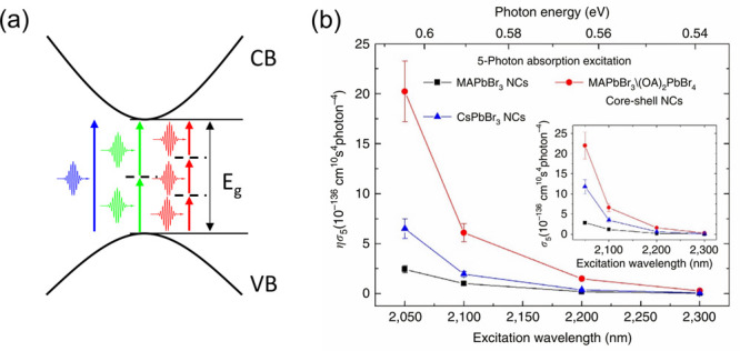
(a) Schematic of multiple photon absorption process. (b) Five-photon action cross-section ησ5 as a function of pump wavelength for CsPbBr3, MAPbBr3, and core–shell MAPbBr3@(OA)2PbBr4 NCs. The inset is σ5 as a function of pump wavelength for these three samples. Reproduced with permission from ref (139). Copyright 2017 Nature Publishing Group.
The MPA process usually occurs under intense light excitation because of a much lower MPA coefficient. In general, the MPA coefficient depends on the pump energy and decreases with increasing order. For 3D dielectrics and inorganic semiconductors with a two-band model, the energy-dependent absorption coefficient α2 for absorbing two identical photons can be estimated as142
| 5 |
where K is the material-independent
Kane parameter, n0 is the linear refractive
index,  is the dispersion function with Θ(x) the Heaviside step function and x =
ℏω/Eg, Ep = 2Pvc2/m0 is a nearly
material-independent constant (∼21 eV for most direct bandgap
semiconductors142) related to the oscillator
strength magnitude with Pvc being the
momentum matrix element between VBM and CBM. As seen from eq 5, α2 becomes
zero when
is the dispersion function with Θ(x) the Heaviside step function and x =
ℏω/Eg, Ep = 2Pvc2/m0 is a nearly
material-independent constant (∼21 eV for most direct bandgap
semiconductors142) related to the oscillator
strength magnitude with Pvc being the
momentum matrix element between VBM and CBM. As seen from eq 5, α2 becomes
zero when  while it reaches the maximum and has a n0Eg–3 dependence when ℏω ≈ 0.71Eg.
Likewise, for the three-photon absorption process, α3 can be estimated as143
| 6 |
where P is the Kane momentum
parameter. As shown in eq 6, α3 shows a n0–3Eg dependence
when it reaches its maximum at 0.46Eg.
For the estimation of other high-order nonlinear absorption coefficients,
one can refer to previous work by Wherrett et al., which demonstrates that  .143
.143
MPA coefficients for n ≤ 3 are typically measured using the open-aperture Z-scan nonlinear spectroscopy or nonlinear intensity-dependent transmission spectroscopy, whereas that of high-order MAP processes (i.e., n > 3) are usually characterized using multiple-photon excited PL spectroscopy.139,144,145 This is because of the much lower detection efficiency for higher-order MPA process which requires extremely high pump intensities in the open-aperture Z-scan measurement that would inevitably introduce some artifacts and cause sample degradation.
MPA coefficients of HPs have been well characterized in films, SCs as well as colloidal NCs with reported values spanning over a few orders of magnitude.146−148 The large variation of these reported values is likely because MPA coefficients are strongly affected by the chemical composition, quantum confinement, the presence of structural defects, etc. It has been found that α2 are on the order of a few to 102 cm/GW in 3D perovskite films149−151 and SCs,144,152−155 whereas α3 on the order of 10–4 to 10–1 cm3 GW–2 have been reported in 3D perovskite SCs.152,153,155,156 Meanwhile, due to giant oscillator strength (because of structural and dielectric confinements as well as the presence of real intraexcitonic states), 2D HPs have been found to exhibit much larger MPA coefficients, with α2 in the range of 10–2 × 105 cm GW–1 and α3 in the range of 0.5–2.5 cm3 GW–2 compared to their 3D counterparts at the same excitation wavelength.151,157−160 On the other hand, unlike bulk materials, the MPA strength of perovskite NCs is usually quantified by their MPA cross sections σn = (ℏω)n−1αn/(2nN0d0), where N0 and d0 are the Avogadro’s number and molar concentration, respectively. σ2 as large as 106 GM (i.e., 1 Goeppert Mayer (GM) = 10–50 cm4 s/photon) have been reported in bromine and iodine perovskite NCs139,161−163 that are 1–2 orders larger than those of a large-size CdSe/CdS dot164,165 and are 2–3 orders larger than conventional inorganic semiconductor NCs166−169 as well as organic chromophores.170−172 Meanwhile, σ3 as large as ∼1.1 × 10–73 cm6 s2 photon–2 has been reported in CsPbI3 NCs,162 which is more than 3 orders higher than those of conventional CdSe quantum dots173 and the reported organic molecule.174
Other than exhibiting superior two-photon and three-photon absorption cross sections, perovskite NCs also possess notably higher-order MPA cross sections. In particular, our group discovered that colloidal perovskite CsPbBr3, MAPbBr3, and core–shell MAPbBr3@octylammonium lead bromide ((OA)2PbBr4) NCs possess giant MPA cross sections, with five-photon action cross sections ησ5 ∼ 10–136 cm10 s4 photon–4 (here η is the PL quantum yield) more than 9 orders of magnitude larger than that of the state-of-the-art organic molecules (Figure 5b).139 Even larger MPA is possible with core–shell MAPbBr3@(OA)2PbBr4 NCs, which may be due to the synergetic effects of effective surface passivation,175,176 photoinduced screening of the internal field,176,177 nonradiative energy transfer from the shell to the core via antenna-like effect,164 dielectric confinement,176 and local field effect,176,178etc. Reports by other groups139,146,179 concur with our findings on these unique nonlinear properties, thus rendering HPs as highly promising for nonlinear optics application in light amplification,180,181 bioimaging,182 and ultrafast laser modulator,183etc. Detailed discussion of these nonlinear properties and their applications are beyond the scope of this work. Interested readers are referred to the recent reports.146,147,184
3.2. Ultrafast Carrier Thermalization
The initial photoexcitation of a semiconductor by a laser creates a population of carriers in the electronic bands that depend on the spectrum of the excitation source and the DOS. Initially, these carriers possess an energy equal to the excitation energy and are hence not in thermodynamic equilibrium. After undergoing ultrafast scattering processes that primarily include carrier–carrier and carrier–phonon events, the energetic distribution of the carriers gradually broadens and can be described by a quasi-thermalized Fermi–Dirac distribution with a temperature greater than the lattice temperature TL.185,186 It is important not to confuse carrier thermalization with carrier cooling; the latter is sometimes referred to as “thermalization” in the literature. The carrier thermalization process precedes carrier cooling, and the main difference between the two is that the latter involves energy losses to the lattice through inelastic scattering events, while the former mainly involves a redistribution of excess energies among the carrier population through elastic scattering events, broadening the energetic distribution of the carriers such that they form a Fermi–Dirac distribution.
In GaAs, it is widely accepted that this process occurs within a few hundreds of femtoseconds, although values up to a few picoseconds have been reported depending on the system and experimental technique.185−187 Such an ultrafast process demands high time resolution in the technique used. The widely used transient absorption (TA) spectroscopy with typical ∼100 fs time resolution is deemed inadequate for HPs. Other spectroscopy techniques with better time resolution are required, such as the two-dimensional electronic spectroscopy (2DES) which extends the time resolution down to ∼10 fs or better. Distinct from 1D TA spectroscopy, 2DES employs a pair of phase-locked pump pulses with time separation called coherence time τ to excite the sample followed by monitoring the absorption or transmission change of the sample by another probe pulse delayed by the waiting time T with respect to the second pump pulse. The resulting data is then plotted as a 2D spectrum, with one axis representing the excitation frequency and the other axis representing the emission frequency. This 2DES technique is especially powerful to investigate the quantum coherence between different excited states as well as the excited state transition to a high-energy state. A detailed description of the 2DES technique is beyond the scope of this review. The interested reader is directed to a recent review by Scholes et al. for further reading.188
Richter et al. conducted 2DES with sub-10 fs time resolution on archetypal MAPbI3 thin films to study the carrier thermalization process.183 The sub-10 fs time resolution of their 2DES setup adequately resolves the decay kinetics into 3 well-separated regimes ascribed to dephasing, thermalization, and subsequent cooling processes (Figure 6a). The ΔT/T spectra at pump wavelength of 625 nm are shown in Figure 6b for several delay times. At time zero, a peak is seen roughly around the pump wavelength, which indicates the initial creation of the nonthermalized carrier population by the pump. Over the next ∼50 fs, redistribution of excess energies among the carriers through scattering events proceeds, and this peak broadens toward the band-edge (∼750 nm) with a spectral line shape resembling a Fermi–Dirac distribution function with a carrier temperature Tc greater than the lattice temperature TL. By ∼100 fs, the peak position shifts toward the band-edge, indicating that the carrier thermalization process has completed. The authors also compared the excess energy dependence of the thermalization process (Figure 6c,d). The decay kinetics probed at wavelengths corresponding to the excitation, above excitation, and at the band-edge were monitored at two different pump wavelengths. The two pump wavelengths of 662 and 720 nm correspond to the cases with larger and smaller excess energies, respectively. They found that the carrier thermalization proceeds faster with larger excess energies with the thermalization time constant for 720 nm pump (∼45 fs) being 3 times larger than that of the 662 nm pump (∼15 fs). Furthermore, the authors found that the thermalization time reduces with larger photoexcited carrier densities.
Figure 6.

(a) Spectral kinetics of MAPbI3 films pumped at 655 nm and probed at 695 nm measured using 2DES. The kinetics can be well-separated into 3 regimes as described. (b) ΔT/T spectra at several delay times obtained with 625 nm pump. Spectral kinetics probed at different wavelengths for the 662 nm (c) and 720 nm (d) pumps, respectively. The insets of all panels show the spectral positions of the obtained kinetics on the 2D map. Reproduced with permission from ref (183). Copyright 2017 Nature Publishing Group.
These observations can be rationalized by considering the average group velocity of the carriers. With larger excess energies and, hence, kinetic energies of individual carriers, carrier scattering rates will increase, thus facilitating the carrier thermalization process. The carrier thermalization process can in general proceed through carrier–carrier, carrier–phonon, and carrier–impurity scattering events. The observed decreased thermalization times that implies increased scattering rates with both increasing pump energy and photoexcited carrier density strongly suggests that carrier thermalization proceeds by carrier–carrier scattering. The carrier–carrier scattering process is mediated by Coulombic interactions within the carriers. In general, the scattering rate can be derived from the Boltzmann equation given as189
| 7 |
With the scattering probabilities, Se±(k) proportional to the scattering amplitude |M|2 given by
| 8 |
The factor 1/|ε|2 is the screening factor that determines the effective Coulomb interaction between individual carriers and, hence, the scattering rate. The optical dielectric constant ε of MAPbI3 is 6.5,121 about half that of GaAs. This explains the roughly twice as fast carrier–carrier scattering process observed at similar excitation densities in MAPbI3. The authors further highlight that this ultrafast thermalization process limits the efficiency of HC extraction in HC solar cells, a conceptualized next-generation solar cell device that could potentially harness the excess energies of these HCs to further boost the efficiencies of current solar cells. The reader is directed to recent reviews by our group and Loi et al. for further discussions on HC perovskite solar cells.27,190
4. Hot Carrier Trapping, Cooling, and Transport Dynamics
Following the carrier thermalization process, the photoexcited carrier distribution is still out of thermal equilibrium with respect to the lattice (i.e., Tc > TL). Thus, the subsequent photophysical processes in the next few picoseconds largely involve these HCs. These sequential processes will be covered in detail in the following sections.
4.1. Hot Carrier Trapping
Due to the unique electronic structure of HPs, the intrinsic trap states tend to lie close to the band-edge which is considered shallow, thus bestowing HPs their unique defect tolerance.82,191−193 While these shallow trap states are perceived as benign and give rise to excellent optoelectronic properties of HPs such as long charge carrier lifetimes and diffusion lengths,193,194 their impact on HC relaxation has only recently been questioned. Given the great potential of HPs for HC solar cell applications, the impact of shallow traps on HC relaxation is of particular concern as it would limit the efficiency of HC extraction through the hot charge acceptors in an HC solar cell device. In the following sections, we examine the HC trapping phenomena in HPs.
4.1.1. Hot Carrier Trapping in Bulk Halide Perovskites
In polycrystalline HP films, it is well-established that defect sites are much more abundant at the interfaces and grain boundaries (GBs).195,196 GBs are part and parcel of polycrystals, while interfaces are also inevitable in a practical device with multiple layers of different materials. Jiang et al. performed a comparative study of the carrier dynamics at the GBs and grain interior (GI) using the transient absorption microscopy (TAM) technique (Figure 7).197 In contrast to conventional 1D TA spectroscopy in which spectroscopic information represents a spatial ensemble average in the weakly focused probe beam, the TAM technique images the excited state dynamics spatially over individual microscopic areas of the sample, thereby permitting distinction of GIs versus GBs. Readers interested in a detailed description of this technique are referred to previous reviews.198,199 A comparison of the TA spectra monitored at the GI (Figure 7b,c) and the GBs (Figure 7d,e) shows a marked difference in the spectral features and dynamics.
Figure 7.

Observation of sub-bandgap states that act as fast HC relaxation pathways in MAPbI3. (a) Representative SEM image (scale bar 1 μm) of a single particle that comprises multiple grains in the MAPbI3 film. The black dashed lines denote the grain boundaries. (b) and (d) pseudocolor TA surface plot and (c) and (e) TA spectra at several time delays at points corresponding to the grain interior (GI) and grain boundary (GB), respectively. The black solid line in panel (c) and (e) denote fits to a band-filling model and the red arrow in panel (e) denotes the appearance of a sub-bandgap feature. (f) Dynamics of the spectrally integrated sub-bandgap feature extracted from the fits; the solid line is an exponential fit yielding the lifetime indicated in the panel. (g) TA spectra at 1.8 and 1.0 ps along with their fits to the model (black solid line) and the residuals (dashed line). Modified from ref (197). Copyright 2019 American Chemical Society.
While the general spectral shape at both regions is similar, the GB spectra show an obvious sub-bandgap feature that grows within the first few picoseconds (Figure 7e), a feature that is absent at the GIs (Figure 7c). The authors then adopted a band-filling model to fit the entire TA spectra. However, as the model does not account for this sub-bandgap state, the extracted fitting residuals are used as a quantitative indication of the density and energetic position of the sub-bandgap state. As seen in Figure 7g, the sub-bandgap state peaks around ∼1.57 eV, about ∼60 meV below the bandgap of ∼1.63 eV. Spectral mapping of the residuals over the entire particle confirms that this sub-bandgap state is largely concentrated around the GBs, i.e., along the dotted lines marked in Figure 7a. Furthermore, a comparison of the high-energy region of the TA spectra between the GI and GB (Figure 7c,e) shows that the carrier temperatures are higher at the GIs than at the GBs. Indeed, the authors further observed in the cooling curves that the HCs at the GIs have a higher initial carrier temperature and cool slower than at the GBs, suggesting that the sub-bandgap states promote a faster HC cooling behavior. Additionally, the decay in the carrier temperature and concomitant rise in the intensity of the sub-bandgap feature is further accompanied by a rise in the quasi-Fermi level (EF) at the GBs. The authors attributed this rise in EF to the trapping of only one type of charge carrier, causing the sub-bandgap state to be charged. They further attributed this sub-bandgap state to a hole-trapping state near the VBM that forms from a defect induced by the termination of the I–I bond at the GB. Importantly, the impact of these seemingly benign shallow defect states on HCs has serious implications for utilizing HPs for HC solar cells, as these sub-bandgap states will influence both the carrier temperatures and extraction efficiencies of the HCs. Thus, strategies to passivate or manage the abundance of these sub-bandgap states are crucial for HC applications.
4.1.2. Hot Carrier Trapping in Halide Perovskite Nanocrystals
Besides polycrystals that are rich in defect sites at the GBs, semiconductor NCs with their high surface-to-volume ratio provide another excellent platform to examine carrier trapping behavior. Perovskite NCs have also recently attracted considerable attention because of their defect-tolerant nature, which gives rise to their highly emissive properties advantageous for optoelectronic applications.200 The abrupt termination of the crystal lattice at perovskite NC surfaces results in defect sites that are usually coordinated with passivating ligands that could also detach.201,202 This raises fresh questions on the defect-tolerant nature of perovskite NCs, particularly on the effect of these surface traps that act as shallow defects on HCs. Whether such defects play a role in influencing HCs is also a matter of much debate in traditional semiconductor NCs such as CdSe with recent experimental observations confirming this role.203−205 Given NCs' intrinsic large surface-to-volume ratio, approaches to effectively control these surface traps via ligand modification is imperative.201 Fortunately, there exists a large library of ligands that could passivate these surface traps to different degrees.
A recent HC trapping study in MAPbI3 and MAPbBr3 NCs by our group uncovered an excitation energy dependence in the photoluminescence quantum yield (PLQY) from their photoaction spectra, where their PLQYs reduce with increasing excess energies (δE) with respect to the bandgap energy of the perovskite NCs (Figure 8).206 This dependence of PLQY with δE suggests a loss in carriers that facilitate radiative recombination with increasing δE, and indicates an alternative nonradiative trapping channel that opens up with increasing δE. This trend is observed in both MAPbI3 and MAPbBr3, regardless of their absolute QYs, which indicates the influence of this trapping process on HCs that becomes significant with higher δE. This provides the first evidence of the potency of these traps toward HCs despite the perceived benign nature of traps in HPs.
Figure 8.

HC trapping in perovskite NCs. (a) Schematic of the Marcus charge transfer model depicting the interaction between carriers and shallow trap states. The trapping rate (kT) is influenced by the magnitude of the excess energy (δE), reorganization energy (λ), and free energy associated with the trapping process (ΔG0). Illustrations for the high excess energy (b) and low excess energy (c) cases, where larger excess energies increase the trapping rate and hence the fraction of trapped carriers. PLQY as a function of δE for (d) MAPbI3 and (e) MAPbBr3 NCs with and without TOPO treatment (f) pump–probe (PP) and pump-push-probe (PPP) kinetics of MAPbI3 pumped at 1.91 eV, probed at 1.70 eV and pushed at 1.03 eV. The solid lines are exponential fits to the data. Reproduced with permission from ref (206). Copyright 2020 Nature Publishing Group.
To explicate the interaction of HCs with these trap states, we developed a model based on the Marcus theory for charge transfer (Figure 8a), which was previously applied to describe the trapping processes in CdSe NCs.207,208 In this framework, the free and trapped carriers are on different potential surfaces (represented by their respective parabolas in Figure 8a) that are separated in nuclear coordinates. The trapping rate (kT) that dictates the number of trapped HCs is influenced by the magnitudes of δE, the reorganization energy λ, and the free energy associated with the trapping process ΔG0. kT can be expressed as
| 9 |
where HS is a constant describing the electronic coupling between carriers and traps, TL is the lattice temperature, and ℏ is the reduced Planck’s constant. The time evolution of the population of nontrapped (N) and trapped (NT) carriers can be described by the coupled rate equations:
| 10 |
| 11 |
where k2, knr, and ϵ are the radiative bimolecular recombination rate constant, nonradiative recombination rate constants, and the energy axis, respectively. The first term on the right-hand side of eq 10 represents the population decay due to carrier recombination, whereas the second and last terms refer to the contribution from the trapping of nontrapped carriers and the detrapping of trapped carriers, respectively. Note that eq 10 describes the dynamics of free carriers. And when excitons are involved (e.g., for the more excitonic MAPbBr3), eq 10 is modified by replacing k2N2 with k1N, where k1 is the monomolecular recombination rate constant. Finally, the PLQY for the case of free carriers can be expressed as
| 12 |
Here, N0 is the initial photoexcited carrier population. As evident from eq 10, a larger δE promotes a greater degree of HC trapping through an increase in the trapping rate kT. The two situations of lower and higher values of δE are illustrated in Figure 8b,c, where HCs possessing larger δE experience a larger driving force promoting them into the potential surface of the shallow traps. The model reproduces the trend in PLQY values for both perovskite NC compositions (Figure 8d,e), confirming that PLQY reduction with increasing δE indeed originates from carrier loss resulting from HC trapping. Pump-push-probe (PPP) measurements further substantiate these findings (Figure 8f). The PPP technique is like the pump–probe (PP) or TA technique but with the addition of a third push pulse, which serves to re-excite a portion of band-edge cold carriers. The transients were collected with a 1.91 eV pump and 1.03 eV push pulses and probed at the main photobleaching (PB) peak position of MAPbI3 (1.70 eV). From the transients, the push pulse causes a reduction in the bleaching intensity due to the re-excitation of the band-edge carriers. This bleach intensity recovers fully within ∼1 ps, on a time scale similar to the HC cooling time. However, while complete recovery of the bleaching intensity is observed, the dynamics following the bleach recovery exhibit a faster decay with an additional fast component with a lifetime of ∼100 ps. This suggests that the re-excitation of the band-edge cold carriers into their energetic “hot” states opens a new faster recombination channel. Moreover, PP transients obtained with δE = 0.8 eV shows a shorter lifetime than that obtained with δE = 0.4 eV. These observations corroborate our δE-dependent PLQY results and strongly supports that HC trapping into shallow trap states induces this faster recombination. Additionally, Figure 8d,e shows that the HC losses are diminished with TOPO added, which is a stronger binding ligand that serves to reduce the carrier-trapping coupling HS, as inferred from the fits with eq 12. This shows that these shallow traps could be passivated to some degree to mitigate the carrier losses.
Notably, the implications of HC trapping and the excitation energy dependence of PLQY are that the energetic alignments and interface passivation must be carefully considered for HP applications, employing high energy excitations. These include HC solar cells, multiple exciton generation, amplified spontaneous emission, and PeLEDs, etc. Nonetheless, HC trapping-induced carrier losses can be managed for efficient device operation.
4.2. Hot Carrier Cooling Dynamics
The seminal discovery of slow HC cooling properties in perovskite materials is one of the highlights of spectroscopic studies on their intrinsic optoelectronic properties, which has spawned a very active branch of research. In this section, we follow the studies leading to the discovery of this phenomenon, the underlying mechanisms, and the procedures to extract relevant metrics that characterize the HCs.
4.2.1. Observation of Slow Hot Carrier Cooling
The first report of slow HC cooling properties in HPs can be traced to one of our early papers.89 Utilizing ultrafast TA spectroscopy, the main PB transitions at 480 and 760 nm in MAPbI3 thin films are selectively excited using different pump wavelengths. Compared to the lower energy excitation of 600 nm, the dynamics obtained with 400 nm excitation showed a sequential faster (∼0.4 ps) decay component with a concomitant rise of the 760 nm PB signal, as seen in Figure 9a,b. By conducting further studies of HP thin film separately interfaced with charge accepting layers PCBM and Spiro-OMeTAD, this ∼0.4 ps decay time was attributed to the hot hole intraband cooling time (Figure 9c). A subsequent study confirmed that the hot electrons also relax with a similar lifetime.88
Figure 9.

Observation of slow HC cooling in HPs revealed by TA spectroscopy. (a) TA kinetics of CH3NH3PbI3 (MAPbI3) thin film probed at 480 nm (black □) and 760 nm (red ○) and pumped at (a) 400 nm and (b) 600 nm. (c) Energy alignment scheme of the CB and VB in MAPbI3 interfaced with PCBM and Spiro-OMeTAD. The blue and red arrows depict the transitions monitored by the two probe wavelengths in panels (a) and (b), as indicated. (a–c) Reproduced with permission from ref (89). Copyright 2013 American Association for the Advancement of Science. (d) Pseudocolor plot of the normalized TA spectra of MAPbI3 thin film pumped at 400 nm, with an initial photoexcited carrier density of n0 ∼ 6 × 1018 cm–3 and (e) the corresponding normalized TA spectra at several time delays between 0.1 ps and 3 ns. The red solid lines denote the fitting with a Maxwell–Boltzmann model to extract the carrier temperatures. (f) Cooling curves for various HP thin films and GaAs. All the curves were extracted from the TA spectra collected at similar conditions as in panels (a) and (b). (d–f) Reproduced with permission from ref (110). Copyright 2016 Nature Publishing Group.
Notably, this ∼0.4 ps cooling time is much slower than the typical ∼0.1 ps time in organic semiconductors.210 Later, Yang et al. reported that the high carrier temperatures in HPs could be sustained up to the picoseconds time scale.110 The authors utilized TA spectroscopy with high energy pump (400 nm) excitations at moderate to high initial carrier densities. A broadening of the main PB peak that originates from state-filling at the band-edge was observed. The broadening is particularly obvious within the first few picoseconds and toward the high-energy region (Figure 9d,e). Since the PB signal monitors the occupancy of states, this suggests the presence of highly energetic HCs residing in electronic states above the band-edge. To characterize the HCs, the authors adopted a Maxwell–Boltzmann (MB) fitting method to extract the HC temperatures (Tc) through the fitting of the normalized TA spectra as seen in Figure 9e. Similar studies were performed on different perovskite thin films and GaAs for comparison, and the carrier cooling curves (Tc as a function of time) is shown in Figure 9f. Remarkably, Tc in perovskites can be sustained for even longer, up to ∼100 ps as compared to ∼5 ps for GaAs. These reports sparked renewed interest in HP for advanced photovoltaic concepts like HC solar cells and carrier multiplication solar cells. A slew of HC studies that followed confirms the novel slow HC cooling properties in other HP compositions22,211−216 and in perovskite nanomaterials.19,20,24,25,183
4.2.2. Determination of Hot Carrier Temperature
Apart from the cooling lifetime, other thermodynamic quantities related to the HCs are equally important for device development. Hot carrier temperature (Tc) and the associated cooling curve remains an important metric to characterize the cooling process of HCs. In this section, we detail the methods in the literature to extract the Tc from spectroscopic data. We will discuss the two most widely utilized spectroscopic techniques to study HC dynamics, namely TA and PL spectroscopy.
4.2.2.1. Transient Absorption Spectroscopy
TA spectroscopy, with a typical ∼100 fs time resolution, is one of the most widely used tools to study the carrier dynamics of HPs. This time resolution is sufficient for resolving the HC cooling dynamics post carrier thermalization, where HC dynamics are dominated by phonon interactions.22,110 As briefly mentioned in the previous section, the hallmark of HCs in the TA spectra of HPs is the high-energy broadening of the main PB peak, or more commonly referred as a “high-energy tail” by the community. This is especially obvious at short time delays within the first 1 ps post excitation, as seen in Figure 9d,e and Figure 10a,b. This high-energy tail decays within a few tens of picoseconds, on the time scale equal to the HC cooling time. There are generally two ways to extract Tc from the TA spectra of HPs, namely, a partial spectral fit with an MB distribution as an approximation, or a more rigorous full-spectrum fitting method based on a band-filling model.
Figure 10.

Determination of HC temperature from fitting of spectroscopic data. Illustration of fitting performed on TA data using (a) the Maxwell–Boltzmann (MB) fitting approach and (b) a full-spectrum fit approach with a band-filling model. Illustration of fitting performed on PL data using (c) the MB approach on time-resolved PL data and (d) full spectrum fit approach based on Planck’s radiation law. (a) Reproduced with permission from ref (22). Copyright 2017 Nature Publishing Group. (b) Reproduced from ref (217). Copyright 2020 American Chemical Society. (c) Reproduced with permission from ref (211). Copyright 2018 Nature Publishing Group. (d) Reproduced from ref (218). Copyright 2022 American Chemical Society.
In the first method, the Fermi–Dirac distribution of HCs can be approximated with a MB distribution function for energies greater than the quasi-Fermi energy (i.e., E ≫ EF) so that the high-energy tail can be fitted with110,219
| 13 |
Here, ΔA(E) is the TA spectra at the high-energy tail and A0(E) is the absorption spectrum before excitation. As seen in Figure 10a, the high-energy tail of the PB peak can be well-fitted with eq 13 to extract the Tc for several time delays and construct the cooling curves. This method is convenient and has low computational requirements because the form of eq 13 is mathematically straightforward. Notably, this approximation is adopted from the Group III–V semiconductor community185,219−221 and was used heavily in the 1980s. With more capable modern computers, recent studies have advocated for more comprehensive methods.222−224 Nonetheless, to date, this MB method remains prevalent because of its convenience.
In a recent study, our group highlighted the shortcomings of the MB fitting method and how they can be addressed.217 Particularly, the widespread MB fitting approach has resulted in different reports adopting different variations of the fitting method; a lack of a general consensus on how and where the fitting window should be fixed has limited the comparability of Tc from different reports. In our study, we pointed out that variations in this fitting window over the rather arbitrarily defined region of interest will lead to different values of Tc being obtained. Furthermore, the MB approach ignores any spectral broadening effects, which we show can also significantly exaggerate Tc. Nevertheless, we reaffirmed that the underlying fundamental Physics in the carrier cooling process using this method is largely unaffected. Hence, the MB approach is still a very useful “back of the envelope” method for a quick estimate of Tc.
More thorough full-spectrum fitting techniques are needed when accuracy in the absolute values of Tc is essential for a judicious choice of interface layers for HC device architecture development. We propose a simple band-filling model that includes the necessary thermodynamic quantities to fully describe the TA spectrum of HPs:
| 14 |
Here, ΔA is the TA signal (change in absorption), fe is the Fermi–Dirac distribution function, and A0 and Aexc are the absorption spectrum before and after excitation, respectively. The key point in using eq 14 is in the accurate description of the absorption terms (Aexc and A0) that depend on the DOS. These terms should not be treated as constants, which would compromise the underlying Physics. In most HP compositions, the Elliott equation (eq 1) can sufficiently describe the absorption spectrum, as detailed in an earlier section. With both eqs 1 and 14, the TA spectrum of HPs can be accurately modeled (Figure 10b). Thus, thermodynamic quantities such as EF and Tc associated with fe can be retrieved from the fitting of the TA spectra at several time delays to construct the cooling curves.
4.2.2.2. Time-Resolved PL Spectroscopy
PL-based spectroscopy, such as time-resolved PL (TRPL, Figure 10c) or steady-state PL (SSPL, Figure 10d) spectroscopy, is another common method to study the HC dynamics of HPs. However, because typical time resolutions of TRPL spectroscopy are limited to tens of picoseconds and only detect the emissive species, the HC signature may not be as obvious in these techniques. Nevertheless, under intense photoexcitation, several studies have reported the observations of hot PL in various HPs.11,211,218,225,226 The presence of HCs in the PL spectrum manifests as a similar high-energy tail signature in the main PL peak (Figure 10c,d). For TRPL spectra, the high-energy tail is more obvious in the first few tens of picoseconds post excitation and decays typically within the first nanosecond. For SSPL spectra, the high-energy tail grows with increasing excitation fluence (Figure 10d) because of the increasing likelihood of hot PL emission at high carrier densities. A blueshift is also commonly observed with increasing fluence, and its origins will be discussed in the later section. To extract Tc, two similar approaches are involved, namely, with a similar MB fitting approach and a full-spectrum fit approach based on a model.
The MB fitting approach is straightforward like the TA case, where the high-energy region of the PL peak is fitted to a modified equation similar to eq 13:
| 15 |
Here, IPL is the PL intensity and Teh is the carrier temperature. The high-energy tail of the PL spectra generally conforms well to eq 15, as seen in Figure 10c, where the fits are denoted by red solid lines. However, we reiterate that this approach tends to overestimate Teh as certain considerations such as energy-dependent DOS and broadening effects are usually neglected. A recent study by Savill et al. showed that greatly exaggerated values of Teh could be achieved for samples possessing large spectral broadening effects.224 Thus, values of Teh obtained through this method should be treated with caution.
Concerned about these shortcomings, our group recently proposed a similar full-spectrum fitting approach for the complementary PL spectroscopy technique. Our proposed model is based on Planck’s radiation law:218
| 16 |
where h is Planck’s constant and c is the speed of light in the vacuum. Here, Δμeh represents the chemical potential of radiation or quasi-Fermi splitting and A0(E) is the absorptance of the material. For the derivation details, the interested reader is referred to the publication. Once again, we emphasize the need for an accurate physical model for A0(E), of which either the Elliott equation can be used or a general form that accounts for subgap absorption.227 Using eq 16, we can successfully reproduce the PL line shape of HPs as seen in Figure 10d. The relevant material parameters (bandgap energy Eg, exciton binding energy Eb, and line width Γ) and thermodynamic quantities can be retrieved from the fitting. Hence, with the application of this model on TRPL or SSPL spectra, the evolution of Tc with time or excitation density can be studied to gain insights into the HC dynamics of HPs.
4.3. Slow Hot Carrier Cooling Mechanisms
After ultrafast carrier thermalization, HCs will lose their excess energies by interacting with lattice vibrations or emitting phonons. Due to HPs’ polar nature, the dominant relaxation pathway for HCs is the long-range Fröhlich interaction (i.e., electron-longitudinal optical (LO) phonon scattering arising from Coulomb interactions between the electrons and the macroscopic electric field induced by LO phonon mode) except at very low temperatures when the excess HC energy is less than the LO phonon energy. To account for the distinct HC cooling phenomena in HPs, fluence-, chemical composition-, and dimensionality-dependent cooling mechanisms have been proposed. The fluence-dependent slow HC cooling mechanisms include the hot phonon effect,22,110,212,215,228−230 Auger heating effect,19,22,24,26,183,215,231 and band-filling effect,211 whereas the chemical composition and structural dimensionality-dependent HC mechanisms consist of the polaron screening effect,226,232 reduction of electron–phonon coupling strength,19,20,213,214,231,233 and intrinsic phonon bottleneck effect,25,26,234,235etc. (see Table 1 for a summary). It is important to distinguish between the hot phonon effect and the intrinsic phonon bottleneck effect, as they are occasionally referred to as the “phonon bottleneck effect” in the perovskite literature. However, these terms actually represent distinct mechanisms. The hot phonon effect is commonly used in the Group III-V and II-VI semiconductor communities, whereas the intrinsic phonon bottleneck effect is attributed to the quantum dot community. While there is general consensus that the hot phonon effect and Auger heating effect play significant roles in the fluence-dependent slow HC cooling, the mechanisms of the band-filling effect and polaron screening effect remain under debate. This is partly due to the overestimation of HC temperature in fitting the high-energy tail of the PL or TRPL spectrum caused by discounting the effects from the phonon broadening, occupation of excited states, and the energy-dependent DOS.224,236 In the following sections, we will review these mechanisms and discuss their experimental evidence.
Table 1. Summary of the Applicable Conditions (i.e., Material, Morphology, Pump Energy, Carrier Density, Experimental Technique) When the Corresponding Slow HC Cooling Mechanism Takes Effect.
| slow HC cooling mechanisms | material | morphology | pump energy (eV) | carrier density n (× 1018 cm–3) or ⟨N0⟩ | technique | ref |
|---|---|---|---|---|---|---|
| hot phonon effect | MAPbI3 | film | 3.1 | ≥ ∼1.5 | TA | (110) |
| film | 2.25 | ≥ ∼3.2 | TA | (212) | ||
| film | 2.48 | ≥ ∼0.62 | TA | (22) | ||
| film | 3.1 | ≥ ∼91 (hole) | transient XUV absorption | (229) | ||
| FAPbI3 | film | 3.1 | ≥ ∼2 | TA | (228) | |
| CsPbI3 | NCs (17 nm) | 2.48 | ≥ 1.5 or ⟨N0⟩ ≥ ∼2.9 | TA | (237) | |
| NCs (12.1 nm) | 2.48 | ⟨N0⟩ ≥ ∼1.7 | TA | (238) | ||
| MAPbBr3 | film | 3.1 | ≥ ∼2 | TA | (228) | |
| film | 3.1 | ≥ ∼15 | TA | (26) | ||
| CsPbBr3 | film | 3.1 | ≥ ∼9 | TA | (239) | |
| NCs (8.6 nm) | 3.1 | ≥ ∼6 | TA | (239) | ||
| NCs (7.3 nm) | 3.1 | ≥ ∼7 | TA | (239) | ||
| NCs (11–12 nm) | 3.1 | ≥ ∼0.6 | TA | (240) | ||
| CsPbBr3@ Cs4PbBr6 | NCs (13–15 nm) | 3.1 | ≥ ∼1.8 | TA | (240) | |
| CsPbIBr2 | film | 3.1 | ≥ ∼2 | TA | (228) | |
| CsPb(Br0.8Cl0.2)3 | NCs (11 nm) | 3.1 | ≥ ∼0.31 | TA | (241) | |
| Auger heating effect | MAPbI3 | film | 2.48 | ≥ ∼10 | TA | (22) |
| FAPbI3 | NCs film (10 nm) | 3.1 | 1.1 or ⟨N0⟩ ∼ 2 | TA | (24) | |
| Cs0.05(FA0.83MA0.17)0.95Pb(Br0.17I0.83)3 | film | 3.1 | ≥ ∼29 | TA | (215) | |
| MAPbBr3 | NCs (≥4.9 nm) | 3.1 | ⟨N0⟩ ≥ ∼2.5 | TA | (26) | |
| CsPbBr3 | NCs (9.7 nm) | 3.49 | ⟨N0⟩ ≥ ∼2.5 | TA | (231) | |
| FAPbBr3 | NCs (9.2 nm) | 3.40 | ⟨N0⟩ ≥ ∼4.2 | TA | (231) | |
| band-filling effect | FASnI3 | film | 3.08 | ≥ ∼0.5 | Streak camera | (211) |
| polaron screening effect | MAPbBr3 (≥ ∼180 K) | single crystal | 3.08 | ≤ ∼0.07 | TCSPC | (226) |
| MAPbI3 | film | ≥ ∼2.15 | ≤ ∼0.1 | TCSPC | (232) | |
| intrinsic phonon bottleneck effect | FAPbI3 | NCs (7.5 nm) | >2.3 | ∼2 | TA | (235) |
| MAPbBr3 | NCs (≥4.9 nm) | 3.1 | ⟨N0⟩ ≥ ∼0.1 | TA | (26) | |
| FASnI3 | NCs (≤ ∼10.9 nm) | 3.1 | > ∼6 × 10⁻² | TA | (234) | |
| CsPbI3 | NCs (<8.2 nm) | – | – | 2DES | (25) | |
| reduction of electron–phonon coupling strength | CsPbI3 compared to CsPbBr3 | NCs | 1.26Eg | ⟨N0⟩ ∼ 0.1 | TA | (20) |
| CsPbBr3 compared to MAPbBr3 or FAPbBr3 | film | 0.6 (push energy) | < ∼2 | pump-push-probe | (213) | |
| NCs | ≥2.53 | ⟨N0⟩ < 1 | TA | (19) | ||
| MAPbI3 compared to 2D MAPbI3 | nanoplatelet | 3.1 | – | TA | (242) | |
| CsPbBr3 compared to FAPbBr3 | NCs | – | ⟨N0⟩ < 1 | TA | (231) |
4.3.1. Hot Phonon Effect
One of the most widely acknowledged slow HC cooling mechanisms is the hot phonon effect, which has also been termed as the hot phonon bottleneck effect by the perovskite community. The hot phonon effect describes the phenomenon of a reduced carrier energy loss rate through the retardation of the LO phonon decay at high carrier injection densities. To distinguish this mechanism from the intrinsic phonon bottleneck effect, we shall follow the nomenclature hot phonon effect. The hot phonon effect is commonly reported for highly excited polar semiconductors.220,221,243−247 This effect has recently been observed in HPs including bulk films22,110,212,215,228−230 and weakly or intermediately confined NCs.19,239−241,248 Considering that the DOS and HC cooling behavior of weakly or intermediately confined NCs is similar to that of their bulk counterparts, we shall elaborate on this hot phonon effect in bulk HPs.
Akin to conventional semiconductors, when HPs are intensively pumped (n > 1018 cm–3) with enough excess energies of photoexcited carriers, the hot phonon effect will dominate the slow HC cooling process. This is because HC cooling is a cascade process between the carrier density-dependent carrier–LO phonon scattering and LO phonon decay. The competition of these two processes determines the extent to which the hot phonon effect affects the HC cooling. When the perovskites are intensively excited, there will be a nonequilibrium LO phonon population arising from the fast buildup of LO phonon population, which will increase the reabsorption of LO phonons by HCs. This process will thus decrease the net LO phonon emission rate and decelerate HC cooling. One signature of this hot phonon effect is the larger the pump fluence, the slower the HC cooling. In contrast, when the carrier concentration is low (n < 1017 cm–3), the hot phonon effect will be negligible and the HC cooling rate is independent of carrier concentration.221,247,249
The first evidence of this hot phonon effect induced slow HC cooling was reported by Yang et al. in MAPbI3 films using TA spectroscopy.110 HC cooling kinetics was obtained by fitting the high-energy tail of the TA spectrum using a Maxwell–Boltzmann distribution function (eq 13). A higher HC temperature with increasing pump energy was obtained given that more energies are passed to the HCs (Figure 11a). Nevertheless, the estimated initial HC energy is much smaller than the excess energy of photoexcited carriers, which may be due to the thermalization energy loss via carrier scattering with background carriers and phonons. They found that at low pump fluence, the HC cooling kinetics can be well-fitted using the Fröhlich interaction model irrespective of the pump energy (Figure 11a):250
| 17 |
where ℏωLO is the LO phonon energy, TL is the lattice temperature, and τave is the average LO phonon emission lifetime which is determined by the intrinsic Fröhlich interaction process and thereby is independent of the carrier density. However, with increasing carrier concentration, they found that HCs took more time to cool down to the lattice temperature, and the HC cooling curve deviated from eq 17 (Figure 11b), which was attributed to the hot phonon effect. Compared to GaAs, a conventional semiconductor, HC cooling in methylammonium lead iodide films was found to be much slower, which was ascribed to a faster buildup of LO phonon population and slower decay of LO phonons into acoustic phonons. Similar slow HC cooling was also found in formamidinium lead iodide (FAPbI3) films, which was attributed to the intrinsic phonon bottleneck effect in lead iodide perovskites. Notably, one should be cautious about relying on eq 17 to draw conclusions about the hot phonon effect because the calculated energy loss rate depends strongly on the LO phonon energy used that is much larger than the experimental value (∼13 meV).251,252 The extent to which the hot phonon effect affects the slow HC cooling as well as the origin of this hot phonon effect in HPs are still not clear.
Figure 11.

(a) Pump energy-dependent HC temperature as a function of delay. (b) Carrier density-dependent HC cooling kinetics. Dashed curves are the fittings using eq 17. (a,b) Reproduced with permission from ref (110). Copyright 2016 Nature Publishing Group. (c) Carrier temperature as a function of LO phonon emission lifetime for three different perovskite samples with the same initial average carrier density. Reproduced with permission from ref (228). Copyright 2017 Nature Publishing Group. (d) Carrier density-dependent slow HC cooling governed by hot phonon effect in MAPbI3 films. (e) Calculated phonon dispersion spectrum of tetragonal MAPbI3. The yellow and green zones correspond to longitudinal optical and acoustic phonon branches. (d,e) Reproduced with permission from ref (22). Copyright 2017 Nature Publishing Group. (f) Hot electron and hole cooling kinetics in MAPbI3 films measured using optical and XUV TA spectroscopy. The film was excited at 400 nm with an initial carrier density of 9.1 × 1019 cm–3. Reproduced from ref (229). Copyright 2021 American Chemical Society.
In a bid to unravel the origin of this hot phonon
effect, Yang et al.(228) investigated the fluence-dependent
HC cooling kinetics in MAPbI3, FAPbI3, MAPbBr3, and CsPbIBr2 films using TA spectroscopy. At
similar pump fluence, the HC temperatures were found to be higher
in iodide samples compared to bromide samples because of larger excess
energies of HCs in the former. For iodide samples, HC cooling kinetics
can be fitted using a biexponential decay function with the shorter
subpicosecond lifetime insensitive to the pump fluence and the longer
tens to hundreds of picoseconds lifetime increasing with the growth
of the pump fluence. The short and long cooling lifetimes were attributed
to the Fröhlich electron-LO phonon scattering in the absence
and presence of the hot phonon effect, respectively. Similar fluence-dependent
slow HC cooling was also observed in bromide samples. Considering
the absence of a phonon gap between LO and acoustic phonon branches
in the phonon dispersion spectra from DFT calculations, the authors
proposed that the hot phonon effect is due to the up-conversion of
acoustic phonons to optical phonons arising from inefficient heat
dissipation because of perovskite’s low thermal conductivity.
This blocking of heat dissipation in turn reheats HCs and slows down
HC cooling. On the other hand, below 400 K, τave of
FAPbI3 was found to be 10 times longer than that in CsPbIBr2 and around 3 times longer than that in MAPbBr3 (Figure 11c), which
was attributed to a stronger phonon bottleneck effect in FAPbI3 because the overlapping phonons from organic cation with
that of Pb–I network enhances the recycling of low-energy phonon
modes. Nonetheless, several points must be clarified: (a) The physical
significance of describing the HC temperature decay kinetics with
multiexponential decay since it differs from the population decay.
HC temperature relates to the HC population through 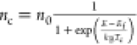 , where n0 is
the photoexcited carrier density and, therefore, may possess different
kinetics. (b) The presence of other processes such as carrier diffusion
and many-body Auger recombination in optically opaque samples (thickness
∼300 nm). Though the average carrier density is on the order
of 1018 cm–3, the incident carrier density
in the front side of the sample is on the order of 1019 cm–3 (or even higher). This local large carrier
density associated with inhomogeneous carrier distribution across
the thick sample could obfuscate the intrinsic HC cooling dynamics
with contributions from carrier diffusion and local Auger recombination.
Besides, the second stage of slow HC cooling that lasts for hundreds
of picoseconds matches that of carrier depopulation by Auger recombination.
(c) It is unclear why the fluence-independent HC cooling due to the
assigned intrinsic Fröhlich interaction is absent in the bromine
samples. (d) Lastly, acoustic phonon branches with negative frequencies
are present in the calculated phonon spectra, which is unusual. (e)
The slower HC cooling rate of iodide samples is consistent with their
weaker Fröhlich interaction strengths, which possess smaller
high-frequency dielectric constants compared to bromide samples.251
, where n0 is
the photoexcited carrier density and, therefore, may possess different
kinetics. (b) The presence of other processes such as carrier diffusion
and many-body Auger recombination in optically opaque samples (thickness
∼300 nm). Though the average carrier density is on the order
of 1018 cm–3, the incident carrier density
in the front side of the sample is on the order of 1019 cm–3 (or even higher). This local large carrier
density associated with inhomogeneous carrier distribution across
the thick sample could obfuscate the intrinsic HC cooling dynamics
with contributions from carrier diffusion and local Auger recombination.
Besides, the second stage of slow HC cooling that lasts for hundreds
of picoseconds matches that of carrier depopulation by Auger recombination.
(c) It is unclear why the fluence-independent HC cooling due to the
assigned intrinsic Fröhlich interaction is absent in the bromine
samples. (d) Lastly, acoustic phonon branches with negative frequencies
are present in the calculated phonon spectra, which is unusual. (e)
The slower HC cooling rate of iodide samples is consistent with their
weaker Fröhlich interaction strengths, which possess smaller
high-frequency dielectric constants compared to bromide samples.251
Our group also conducted a rigorous study of the hot phonon effect on slow HC cooling.22 Starting from the generic Fröhlich electron-LO phonon interaction in the 3D system with a parabolic band structure, the energy loss rate of HCs can be calculated in terms of LO phonon occupation number Nq(T). The LO phonon scattering rate can be then derived from Fermi’s golden rule,253 which gives rise to
 |
18 |
where H′ is the interaction Hamiltonian and f(k) is the Fermi–Dirac distribution of HCs with wave vector k. On the right side of eq 18, the first and second terms describe the LO phonon absorption and emission process, respectively. Eq 18 can be further simplified as
 |
19 |
where Nq(Tc) = 1/(exp(ℏωq/kBTc)–1) is the Bose distribution of LO phonons at
HC temperature Tc, η = Ef/kBTc is the relative quasi-Fermi level. |Mq|2 = 2πℏ2eE0/mq2 is
the transition matrix element. For the expression 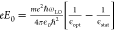 , m is the electron effective
mass, e is the electric charge unit,ℏωq is the LO phonon energy, ϵ0 is the vacuum permittivity, and ϵstat and ϵopt are the static and optical dielectric constants, respectively.
, m is the electron effective
mass, e is the electric charge unit,ℏωq is the LO phonon energy, ϵ0 is the vacuum permittivity, and ϵstat and ϵopt are the static and optical dielectric constants, respectively.
Conversely, assuming a single relaxation time, the LO phonon decay rate can be expressed by
| 20 |
where Nq(TL) = 1/(exp(ℏωq/kBTL)–1) is the Bose distribution of LO phonons at the lattice temperature. Typically, the LO phonon lifetime τph, which is related to the anharmonic interaction between the LO phonon and acoustic phonons, depends on the temperature and the type of phonon–phonon interaction process. Generally, three decay channels exist for LO phonons: the Klemens channel (i.e., one LO phonon decays into two counter-propagating LA phonons),254 the Ridley channel (i.e., one LO phonon decays into an acoustic phonon (TA or LA) and a transverse optical (TO) phonon);255 and the Barman-Srivastava channel (i.e., one LO phonon decays into two TO phonons).256 Among them, the Klemens channel is deemed to be the most efficient for LO phonon relaxation as daughter LA phonons can quickly thermalize with the lattice.257
The energy loss rate of HCs can then be expressed as
| 21 |
where n is the carrier density. In the absence of the hot phonon effect, eq 21 is further simplified as
| 22 |
where K0(x) is the zeroth-order Bessel function and x = ωq/kBT. Eq 22 has the same form but a different prefactor
respective to eq 17.
In the absence of the hot phonon effect, the energy loss rate of HCs
is independent of carrier density, and the HC cooling is much faster
(black curve in Figure 11d). Meanwhile, a carrier density-dependent slow HC cooling
is also shown, which signifies the presence of the hot phonon effect.
Global-fitting of this carrier density-dependent HC cooling yields
a LO phonon lifetime of 0.6 ps (Figure 11d). The estimated LO phonon lifetime is
much longer than the typical electron–LO phonon scattering
time constant of ∼13 fs calculated using 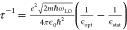 . This is attributed to the suppression
of the efficient Klemens relaxation channel for LO phonons induced
by a large phononic bandgap (ELO >
2ELA) in MAPbI3 (Figure 11e).22 The inhibition of the Klemens channel can be
enhanced when there
is a large atomic mass difference between the oppositely charged ions
that contribute to the LO phonon mode. For instance, a longer LO phonon
lifetime for InP (∼7.6 ps) compared to GaAs (∼2.1 ps)
at room temperature was observed. On the other hand, one can also
accelerate the HC cooling by introducing additional LO phonon relaxation
pathways. For example, Nie et al. reported controlling
HC cooling by interfacial engineering the Fröhlich interaction
in core–shell CsPbBr3@Cs4PbBr6 NCs to enhance the efficient Klemens channel, leading to a faster
HC cooling rate compared to CsPbBr3 NCs.240
. This is attributed to the suppression
of the efficient Klemens relaxation channel for LO phonons induced
by a large phononic bandgap (ELO >
2ELA) in MAPbI3 (Figure 11e).22 The inhibition of the Klemens channel can be
enhanced when there
is a large atomic mass difference between the oppositely charged ions
that contribute to the LO phonon mode. For instance, a longer LO phonon
lifetime for InP (∼7.6 ps) compared to GaAs (∼2.1 ps)
at room temperature was observed. On the other hand, one can also
accelerate the HC cooling by introducing additional LO phonon relaxation
pathways. For example, Nie et al. reported controlling
HC cooling by interfacial engineering the Fröhlich interaction
in core–shell CsPbBr3@Cs4PbBr6 NCs to enhance the efficient Klemens channel, leading to a faster
HC cooling rate compared to CsPbBr3 NCs.240
It should be noted that this fluence related hot phonon effect does not always mean that the hot phonon effect will always be present when a large enough pump fluence is used. Under specific circumstances, this high fluence-induced hot phonon effect can be broken down by the giant electron–phonon coupling interactions. Hintermayr et al. demonstrated that the low dielectric permittivity of the organic ligands results in a reduced Coulomb screening effect of the Fröhlich interaction, leading to a fluence-independent accelerated HC cooling in quasi-2D MAPbI3 nanoplatelets compared to that of quasi-3D MAPbI3 nanoplatelets.242
Further evidence of this hot phonon effect induced slow HC cooling is provided by Sekiguchi and coauthors.230 By exciting the transverse optical (TO) phonons in MAPbI3 films using THz pulses, they observed an increase in HC temperatures associated with a decrease of PL intensity which recovers (within ∼15 ps) after subsequent HC cooling. Because of significant coupling between TO and LO phonons due to strong lattice anharmonicity arising from soft PbI6 octahedron, which is hybridized with MA cation motions, a large population of TO phonons results in direct/indirect up-conversion of TO phonons into LO phonons. This strong perturbation of LO phonon populations in turn leads to a considerable hot phonon effect, which retards HC cooling significantly.
Though the hot phonon effect retarded HC cooling has been intensively investigated, it remains unclear how the hot electron and hole cooling, respectively, respond to the hot phonon effect. The aforementioned studies assumed similar cooling rates between the hot electron and hot hole because of their comparable effective masses. On the other hand, one is unable to differentiate their respective contributions to the carrier cooling curve using the TA or TRPL technique alone since the measured signal is either a sum or product of the electron and hole distribution functions. By combing the optical TA technique with the XUV TA technique which probes the hole’s distribution function, Verkamp et al. resolved the individual hot electron and hole cooling kinetics in MAPbI3 films.229 They found that the initial temperature of the electrons is significantly lower than that of the holes (Figure 11f), which can be attributed to perovskite’s unique band structure of dual VBs with a large DOS in deeper VBM.258 Meanwhile, hot electron cooling was found to be much slower compared to hot hole cooling (Figure 11f) which has a higher onset carrier density for the hot phonon effect. The different cooling rates between hot electrons and holes were attributed to their distinct carrier–LO phonon couplings. They hypothesized that the holes are mainly coupled with LO phonons (∼14 meV) that change the angle between PbI6 octahedra because DOS of VBM is dominated by Pb 6s and I 5p orbitals, whereas the electrons are preferentially coupled with LO phonons (∼29 meV) that displaced Pb within PbI6 octahedra given that DOS of CBM mainly consists of Pb 6p orbitals.75 The larger carrier onset of hot hole cooling was attributed to its smaller Fröhlich polaron radius, which requires a larger carrier density for the polarons to overlap spatially.28 Furthermore, because of the larger effective mass and coupled LO phonon energy, the effective carrier–LO phonon scattering rate τ–1 for the hole is much larger compared to that of the electron. This in turn requires more LO phonons emitted for hot holes to reach the hot phonon bottleneck onset and thus a larger carrier density threshold.
4.3.2. Auger Heating Effect
Apart from the hot phonon effect, the Auger heating effect also plays a significant role when the carrier density is well above 1019 cm–3.19,22,183,215,231 The nonradiative Auger-heating process involves the energy transfer of an electron–hole recombination to another carrier that excites this carrier to an even higher energetic state (Figure 12b).259 Given that this slow HC cooling process occurs only when the nonradiative Auger recombination is present, this stage of HC cooling will show a comparable cooling lifetime to carrier depopulation lifetime due to Auger recombination. The first observation of this Auger heating effect is reported by our group in both MAPbI3 films22 and MAPbBr3 NCs.183 We found that the Auger heating effect can further extend the lifetime of HCs to tens of picoseconds (Figure 12b). Although the transfer of e–h recombination energy does not change the total energy of the e–h pair, the heating of the electronic system will still slow down the HC cooling. The recombination energy transferred to the electronic system is proportional to Eg + E, where Eg is the bandgap.260 The carrier-cooling dynamics including the Auger heating effect can be described as follows:
| 23 |
| 24 |
where n is the initial carrier density, k1, k2, and k3 are the monomolecular, bimolecular, and Auger recombination coefficients, respectively. The first term on the right side of eq 23 is the HC energy loss rate from electron-LO phonon scattering, whereas the second term represents the Auger heating contribution. Eq 24 accounts for the carrier population decay by different orders of recombination processes. The calculated HC cooling kinetics matches well with the experimental data (Figure 12a). The presence of this Auger heating effect is further supported by the observations of rapid shortening of the band-edge PB kinetics that is typical for many-body Auger recombination processes associated with the persistent high-energy tail of hot PL on the long-time scale. The strong Auger heating effect in MAPbI3 at high excitation densities can be assigned to its high Auger recombination coefficient, which is likely due to its relatively small bandgap as well as the coincidental resonance between the bandgap and the interband transitions to a complex high-energy CB.261
Figure 12.

(a) Schematic of hot electron relaxation process via LO phonon emission and nonradiative Auger recombination. The same process can also occur for hot holes. (b) HC cooling kinetics governed by hot phonon (HP) bottleneck and Auger heating (AH) effects at carrier densities above 1019 cm–3. (a,b) Reproduced with permission from ref (22). Copyright 2017 Nature Publishing Group. (c) Energy loss rate as a function of HC temperature for MAPbBr3 NCs with ⟨N0⟩ ∼2.5 and MAPbBr3 bulk film with n0 ∼1.5 × 1019 cm–3. Solid green line represents the LO phonon model at low carrier densities. (d) Normalized HC population decay kinetics at different pump fluences. (c,d) Reproduced with permission from ref (183). Copyright 2017 Nature Publishing Group. HC cooling kinetics under different fluences for FAPbBr3 (e) and CsPbBr3 (f) NCs. Solid curves are fits to the data with single-exponential decay for single electron–hole pair per NC regime and multiple-exponential decay for multiple electron–hole pairs per NC regime. (e,f) Reproduced with permission from ref (231). Copyright 2019 Wiley-VCH.
Compared to bulk films where photoexcited electrons and holes are free to move and thus possess a lower Auger recombination coefficient, the Auger recombination coefficient is expected to be higher262 together with a more significant Auger heating effect in quantum-confined NCs because of momentum conservation and large overlap of the carrier wave functions. Using TA spectroscopy,183 we found that analogous to the bulk films, the initial HC cooling of MAPbBr3 NCs is slowed down by the hot phonon effect, irrespective of the NC size (Figure 12c). Nevertheless, the cooling curve deviates significantly from the Fröhlich scattering model when the HC temperature is below 1500 K. This considerably reduced energy loss rate occurs only when the NCs are intensively excited with an average carrier occupation number ⟨N0⟩ ∼2.5. Conversely, under low pump fluences (⟨N0⟩ ∼0.1), HC cooling follows the hot phonon retarded Fröhlich interaction model. The calculated HC population dynamics also exhibit a biexponential decay with shorter lifetimes (within 1 ps) corresponding to hot phonon delayed HC cooling and longer lifetimes (tens of picoseconds) signifying the Auger heating effect (Figure 12d). Consistently, the longer lifetimes which depend on the NCs’ volume are approximately one-third of the Auger recombination lifetimes.
Likewise, using TA spectroscopy, slow HC cooling retarded by the Auger heating effect associated with the decrease of carrier population was reported in highly excited FAPbBr3 and CsPbBr3 NCs231,19 and in FAPbI3 NCs.24 Consistent with other reports, the larger the pump fluence, the higher the HC temperature and the longer the HC cooling time (Figure 12e,f). Meanwhile, the authors found that the HC cooling lifetimes exhibit multiple-exponential decays only when ⟨N0⟩ > 1, in which faster decay due to Auger recombination occurs (Figure 12e,f). Furthermore, compared to CsPbBr3 NCs, longer HC cooling time due to the Auger heating effect is observed in FAPbBr3 NCs because of its longer Auger recombination lifetime.
4.3.3. Band-Filling Effect
Another proposed
fluence related mechanism is termed the band-filling effect, which
occurs when the band-edge DOS is partially filled by the photoexcited
carriers such that the average energy of the subsequently excited
carriers is larger (Figure 13a).211 This band-filling effect
was first proposed by Fang et al. in tin-based perovskites.
Contrasting with lead HPs, they reported long-lived HCs on a 100 ps
time scale in FASnI3 films at low pump fluence using TRPL
spectroscopy with a streak camera (time resolution ∼10 ps).211 They found that in the time-integrated PL spectrum,
its peak blue-shifts and the slope of the high-energy tail become
gentler with pump fluence, which was ascribed to band-filling of band-edge
DOS (Figure 13b).
Consistently, they found that the transient PL spectrum showed the
same behavior with increasing pump fluence, and the PL line width
became broader (Figure 13c). They further corroborated this band-filling effect from
the blue-shift of the initial PL peak energy with carrier concentration
which follows 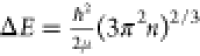 , where μ is the reduced effective
mass, and the decrease of the high-energy tail with delay time in
the transient PL spectrum (see Figure 10c). Meanwhile, the authors found that the
HC temperature decreased from the initial ∼1600 K to ∼750
K within 0.2 ns (Figure 13d). The small valence electronic DOS together with the Rashba-Dresselhaus
effect were thought to play a role in the reduced energy loss rate.
, where μ is the reduced effective
mass, and the decrease of the high-energy tail with delay time in
the transient PL spectrum (see Figure 10c). Meanwhile, the authors found that the
HC temperature decreased from the initial ∼1600 K to ∼750
K within 0.2 ns (Figure 13d). The small valence electronic DOS together with the Rashba-Dresselhaus
effect were thought to play a role in the reduced energy loss rate.
Figure 13.

(a) Schematic of band-filling effect which leads to an increase of optical bandgap when increasing carrier density. (b) Room-temperature transient PL spectra (integrated from 0 to 35 ps) of FASnI3 films at different pump fluences. The sample was excited with a 3.1 eV pump. (c) 2D Contour-plot of transient PL spectrum at different pump fluence of FASnI3 films at room temperature. (d) Extracted HC temperature as a function of time. The red curve is the biexponential decay fit. Reproduced with permission from ref (211). Copyright 2018 Nature Publishing Group.
Although this band-edge DOS band-filling effect gives a phenomenological explanation of the long-lived HCs, it remains unclear how these HCs relax down to the band-edge. Meanwhile, the extracted HC temperature from fitting the high-energy tail of the TRPL spectrum using the simple Maxwell–Boltzmann equation is unable to reflect the real carrier temperature. Besides, the PL line width is greatly affected by the effect of occupation of high-energy states because of inhomogeneous chemical composition as well as phonon and defect broadening, which are omnipresent in solution-processed lead HPs.236,251 Furthermore, Sn-based HPs are known to possess considerable defect densities stemming from the low formation energy of Sn vacancies.194,263,264 Due care must be taken when extracting the HC temperature via fitting the high-energy tail of the TRPL spectrum using the simple Boltzmann equation, especially for HP samples, which possess PL line widths greater than 100 meV, and therefore, the PL line width could have been broadened by the carrier scattering from phonon and structural disorders.224,265
However, the blue-shift observed in the initial PL peak energy with increasing fluence seems to contradict the band-filling effect of the band-edge DOS. The derived reduced effective mass of 0.2m0 (where m0 is the free electron mass) at room temperature is two times larger than the reported 0.08m0.266 Instead, considering that FASnI3 is heavily p-doped because of the low formation energy of Sn vacancies194,263 such that the band-edge PL is dominated by minority carrier–electron population dynamics, the derived effective mass is therefore dominated by the electron effective mass. Nevertheless, based on the band-edge DOS band-filling effect, for the same carrier concentration, MAPbI3–xClx (μ = 0.10m0),124 FAPbI3 (μ = 0.09m0),124 MAPbBr3 (μ = 0.104m0),124 and FAPbBr3 (μ = 0.115m0)124 with smaller reduced effective masses will show a much stronger blue-shift of PL peak energy compared to FASnI3. Furthermore, this large shift of PL peak energy can also occur in band-filling of localized electronic or trap states because of structural disorder (e.g., defects, impurity doping, and inhomogeneous chemical composition, etc.), which has been found in low-temperature PL spectrum of MAPbBr3267 and FAPbI3 films.268 Again, considering the high defect densities of Sn-based perovskites which likely leads to the presence of high-energy localized electronic states, photoexcited carriers can be more easily filled and thus leads to a stronger blue-shift of PL peak energy with carrier density compared to that of Pb-based perovskites.
Regarding the energy relaxation of HCs, given that polar FASnI3 possesses similar effective carrier mass but slightly larger LO phonon energy80 compared to MAPbI3, the dominant Fröhlich interaction is likely to be stronger in FASnI3, which will lead to a faster HC cooling than MAPbI3. Even including the hot phonon effect under low pump fluence, the reduced energy loss rate of HCs due to small DOS of VBM in FASnI3 is unable to account for its long HC cooling lifetime over a 100 ps time scale. The Rashba–Dresselhaus effect is also not likely given that the SOC-induced Rashba–Dresselhaus effect increases with atomic number Z, and thus the Rashba–Dresselhaus effect will be larger in MAPbI3, which does not show very long HC cooling time under low pump fluence.22,212
Apart from the first stage of slow HC cooling, a second stage of residual cooling with a time constant of ∼6 ns was also assigned (Figure 13d). However, this extremely long residual cooling lifetime associated with the redshift of the PL spectrum could also be interfused with the total PL intensity that also decays over the same time scale. Savill et al. attributed this long-lived effect in FASnI3 to the localization of band-edge carriers to the disordered below-bandgap band-tail states stemming from the variation of local potential minimally induced by structural disorders, which can be caused by inhomogeneous oxidation of Sn2+ across the film thickness as well as random orientations of FA cations.224 More studies are warranted to clarify the band-filling effect on slow HC cooling.
4.3.4. Large Polaron Screening Effect
Zhu et al. proposed an alternative mechanism based on the protection by large polarons (i.e., quasiparticles of a charge carrier and the deformed lattice), in which the dressed charge carrier is protected from scattering by LO phonons.226 Reorientational motion of dipolar molecular cations was proposed to result in the formation of large polarons that leads to a much smaller HC cooling rate in hybrid perovskites. Using time-correlated single photon counting (TCSPC), the authors found a high-energy tail in the TRPL spectrum of MAPbBr3 SCs (Figure 14a) at low carrier densities (n ≤ 1017 cm–3), unlike most reports of slow HC cooling observed at large carrier concentrations.11,226,232 This high-energy tail has a shorter lifetime compared to that at the PL peak position, suggesting the presence of two types of carriers. To extract the HC cooling dynamics, the transient PL spectrum (Figure 14b) was fitted using a simple two-temperature model, which gives rise to
 |
25 |
where Eg is the bandgap, T1 and T2 are the temperatures of band-edge carriers and HCs, γ is the ratio of HC concentration to the band-edge carrier concentration, ΔEF is the difference between the quasi-Fermi levels of the electron in the CB and the hole in the VB. The extracted HC cooling curve was then obtained by fixing T1 as the lattice temperature and assuming a constant γ (Figure 14c). They found that the HC temperature first decreases drastically from an initial 1250 ± 200 K with a lifetime of 150 ± 30 ps to ∼850 K and then drops very slowly from ∼0.5 ns to an asymptotic value of 670 ± 100 K (Figure 14c), which is larger than the equilibrium sample temperature of 293 K due to phonon spectral broadening.224,269 A constant ratio γ of (33 ± 5)% was obtained in MAPbBr3. Meanwhile, long-lived energetic carriers were also found in FAPbBr3 but not in CsPbBr3 SCs. This distinct HC lifetime between hybrid perovskites (MAPbBr3 or FAPbBr3) and inorganic CsPbBr3 was correlated with reorientational motion of dipolar molecular cations in the former while absent in the latter. This reorientational motion was proposed to result in the formation of large polarons that protect HCs from scattering by LO phonons which drastically reduces the HC cooling rate. This large polaron formation was also correlated with the temperature dependence of perovskite’s charge carrier transport properties,120,270 as well as their thermal properties.271,272 Analogous to dipole solvation in solution, this polaron was thought to be different from those resulting from the Coulomb potential between charge carrier and inorganic ionic lattice. The reorientational motion of organic cation was supported by time-resolved optical Kerr effect (TR-OKE) measurement with below-bandgap pump and near-infrared probe, in which the hybrid perovskites (MAPbBr3 and FAPbBr3) showed long time response from ∼100 fs to ∼2 ps of rotational motions associated with local-interaction-induced anisotropy and diffusive rotation of the molecular cations, in addition to instantaneous electronic response and ultrafast response from inertial reorientation due to polarization anisotropy that is present in fully inorganic CsPbBr3. The subpicosecond to picosecond TR-OKE response of hybrid perovskites was found to be consistent with that of anisotropic molecular liquids.273
Figure 14.

(a) Pseudocolor plot of room temperature TRPL spectrum of a MAPbBr3 SC microplate pumped at 3.08 eV with a fluence of 1.7 μJ cm–2. (b) Transient PL spectra (filled squares) at different times and the curve-fits (colored curves) using a two-temperature model. (c) Extracted HC temperatures as a function of time. The red curve is a single exponential decay fit in the first 0.5 ns, which yields a lifetime of 150 ± 30 ps. (a–c) Reproduced with permission from ref (27). Copyright 2019 Wiley-VCH. (d) Normalized PL spectra pumped at 3.06 eV with different fluence at peak HC temperature. (e) Carrier density dependent peak HC temperature for different pump fluences. (d,e) Adapted from ref (232). Copyright 2016 American Chemical Society. (f) TR-OKE kinetics of MAPbBr3 (red circles) and CsPbBr3 (blue circles) with above-bandgap pump at 2.30 and 2.38 eV, respectively. The solid curves are the biexponential decay fittings. Reproduced with permission from ref (11). Copyright 2017 American Association for the Advancement of Science.
The critical role of the liquid-like motion of the organic cation on slow HC cooling was later correlated with TRPL measurements of MAPbBr3 SCs in the tetragonal phase (at 180 K) and orthorhombic phase (at 77 K), in which the rotational motion of MA cation is partially hindered in an anisotropic potential and completely frozen. Persistent energetic carriers with a lifetime of ∼150 ps were observed at 180 K but not at 77 K with the high-energy tail absent, which was attributed to the loss of polaron protection because the organic cation motion was fully frozen out.226 This faster cooling of HCs at lower temperatures contrasts with that of conventional polar semiconductors in which the HC cooling time is longer because of the weaker Fröhlich interaction.22 Moreover, the HC temperature was found to be lower at higher carrier concentrations, which is different from the slow HC cooling governed by the hot phonon effect that occurs when the carrier concentration is well above 1018 cm–3. The authors highlighted that the increased HC cooling rate with increasing carrier concentration was due to the destabilization of large polarons stemming from enhanced repulsive interpolaron interaction until the onset of the hot phonon effect.226,232
From the same group, Niesner et al. observed similar persistent energetic carriers in MAPbI3 films using the TCSPC technique.232 The high-energy tail in the initial peak PL spectrum was also found to decline at higher carrier concentrations (Figure 14d). The HC temperature was obtained by fitting the high-energy tail of the transient PL spectrum using the Maxwell–Boltzmann equation. They found that the transient PL spectrum and the HC cooling dynamics are almost the same for pump wavelengths with initial excess energy ΔE larger than 0.5 eV except for the near-resonant pump wavelength. Meanwhile, the peak excess energies of the HCs were found to decrease with increasing carrier concentrations (Figure 14e), which is in contrast with that due to the hot phonon effect. This was explained by the disruption of polaron protection due to the mutual repulsion of polarization clouds. Moreover, using time-resolved two photon photoemission spectroscopy (TR-2PPE), they also observed energetic electrons with excess energy ΔE ≈ 0.25 eV above the CBM with a lifetime of ∼100 ps, which is 2–3 orders of magnitude longer than those in conventional semiconductors.
To verify the presence of large polaron formation, Miyata et al. conducted pump energy dependent TR-OKE measurements in MAPbBr3 and CsPbBr3 SCs.12 By varying the pump energy from well above the bandgap to below the bandgap, they observed distinct TR-OKE kinetics in MAPbBr3: when the pump energy is larger than the bandgap, the TR-OKE kinetics shows a biexponential decay with the shorter lifetime of ∼0.3 ps attributed to polaron formation by photoexcited charges with deformed PbBr3– sublattice and the longer lifetime of ∼3.4 ps ascribed to anisotropy loss (Figure 14f); when the pump energy is below the bandgap, the TR-OKE kinetics mainly displays a response related to organic cation reorientational motion. In comparison, TR-OKE kinetics in CsPbBr3 were found to show similar biexponential decay for the above-bandgap pump with a shorter lifetime of ∼0.7 ps and a longer lifetime of ∼6.5 ps (Figure 14f). Organic cation reorientational motion was thought to contribute to a slightly faster polaron formation rate in MAPbBr3 compared to CsPbBr3.
Nevertheless, this large polaron protection mechanism is still under debate. First, the high-energy tail in the PL spectrum of hybrid perovskites compared to their inorganic counterparts could also arise from high-energy electronic states because of inhomogeneous chemical composition as well as from phonon and defect broadening, which are omnipresent in solution-processed lead HPs.236,251 Meanwhile, the diminishing high-energy tail in the low-temperature PL spectrum of MAPbBr3226 could also be due to a reduced phonon broadening effect. Besides, strong phonon broadening effects are present in both the transient PL226,232 and TR-2PPE spectrum,232 as evident from the extracted asymptotic carrier temperatures. Second, it seems that the correlation between measured TR-OKE response and persistent HCs is vague. The different OKE response for the below-bandgap pump between hybrid perovskites and inorganic perovskite226 is expected given that there is another contribution to the OKE response from the reorientation motion of organic cation, which has a nonzero dipole moment in the former. Indeed, the inverse trend of HC cooling dynamics is widely reported by many groups with fully inorganic perovskites exhibiting longer HC cooling lifetimes compared to the hybrid counterparts.14,19,213,231,233 The breaking of lattice symmetry in hybrid perovskites is likely to increase the phonon’s DOS and enhance the electron–phonon coupling, resulting in a shorter HC cooling time compared to the fully inorganic perovskites.19,213,233 This would also apply to the rotational motion of the organic cation which is likely to enhance the vibration motion of the Pb–I framework and thus lead to a faster HC cooling.233 Meanwhile, for the above-bandgap pump, besides the polaron formation effect, birefringence could also contribute to the biexponential decay of TR-OKE kinetics.12 On the other hand, the phonon vibration induced oscillation from impulsive stimulated Raman scattering (ISRS) will occur whenever the laser pulse duration is shorter than the vibrational period of the Raman-active phonon modes, irrespective of pump energy,274 and these activated phonon modes are independent of pump energy for a single electronic state. Moreover, the distinct OKE response for different excitation energy was later found to be correlated with anisotropy induced birefringence,275 and the observed oscillation in TR-OKE kinetics can be attributed to the dispersive propagation of the probe.275 Both effects should not be related to phonon vibration and large polaron formation. Third, considering that the TR-2PPE spectroscopy (conducted under ultrahigh vacuum conditions) is very sensitive to the sample’s surface and structural disorder from inhomogeneous chemical composition, the observed high-energy state232 may arise from this surface state, which may also disappear at low temperatures. Further studies are warranted.
4.3.5. Reduction of Electron–Phonon Coupling Strength
Apart from exhibiting fluence dependence, HC cooling in HPs also exhibits chemical composition dependence for both the organic cation19,213,231,233 and halide anion.20 Here, we term these dependences as the reduction of electron–phonon coupling strength considering that the equivalent effect is the weakening of Fröhlich interaction. This is because the electron–phonon scattering time constant depends on carrier effective mass, LO phonon energy, and dielectric constant. Since these parameters will be dissimilar for perovskites with different chemical compositions, it is therefore expected that the HC cooling rate exhibits such chemical composition dependence.
Contrasting with the report by Zhu et al.,226 Madjet et al. using nonadiabatic molecular dynamics simulations found that the hot electron cooling rate is smallest in CsPbI3 but largest in FAPbI3, whereas the hot hole cooling rate is smallest in CsPbI3 but similar in MAPbI3 and FAPbI3 (Figure 15a).233 Carrier–phonon nonadiabatic couplings (NAC) between states in both CB and VB were conducted to elucidate the much slower HC cooling rate of fully inorganic CsPbI3 compared to their hybrid counterparts. Figure 15b shows the NAC absolute value averaged over 3.5 ps molecular dynamics trajectories for FAPbI3, MAPbI3, and CsPbI3, where i = 0 and i = 1 correspond to the VBM and CBM states, respectively. They found that the nonradiative transitions most likely occur between adjacent states given the strong NAC strengths along the subdiagonal lines. The NAC amplitude is smaller for states separated by a larger gap, which is expected considering that it is inversely proportional to the difference between the energy levels. Meanwhile, the NAC strength of the VB was found to be much higher compared to that of the CB, which was attributed to its larger DOS. Most importantly, the NAC strength was found to be the smallest in CsPbI3 but largest in FAPbI3, which agreed with their respective HC cooling rates. The much smaller NAC in CsPBI3 was assigned to its much smaller mixture of Cs states into both CB and VB states (Figure 15b).
Figure 15.

(a) Hot electron (top panel) and hot hole (bottom panel) population as a function of time. (b) Average magnitude of the carrier-phonon nonadiabatic couplings for the FAPbI3 (top panel), MAPbI3 (middle panel), and CsPbI3 (bottom panel). (a,b) Modified from ref (233). Copyright 2017 American Chemical Society. (c) Fitted HC cooling time (τcool) as a function of the initial HC density for MAPbI3 by the pump-push-probe technique. The red line is a linear fit. Extracted y-intercept (τcool) and slope are shown in panel (d) for FAPbI3, MAPbI3, MAPbBr3, and CsPbBr3. (c,d) Modified from ref (213). Copyright 2018 American Chemical Society.
Experimental evidence of reduced HC cooling rate in fully inorganic perovskites compared to hybrid perovskites was first provided by Hopper et al. using the ultrafast PPP technique.213 This PPP approach, which employs a third IR push pulse to elevate a fraction of the photoexcited carriers into the high-energy state, enables one to study the HC cooling behavior with variable HC density without using high pump power that may complicate the analysis arising from the many-body Auger effect and spectral broadening from phonon scattering, etc. Concurrent with the re-excitation of cold carriers into the high-energy state, the band-edge PB amplitude will be reduced. After HC cooling, the energetic carriers will relax back into the cold carrier reservoir with a monoexponential decay time τcool, resulting in a recovery of the PB amplitude. Systemic HC cooling dynamics of perovskites with different A cation and halide anions, and different HC densities controlled by the push pulse fluence were investigated. It was found that the HC cooling times of all the perovskites increase steadily with the growth of pushed HC density (Figure 15c), which was attributed to the hot phonon bottleneck effect within the polaron framework. Meanwhile, a linear dependence of HC cooling time on HC density was found, with τcool at n0hot = 0 being the largest in the iodide samples, while the slope is largest in the fully inorganic CsPbI3 compared to hybrid perovskites (Figure 15d). The much steeper dependence of τcool on the HC density in the fully inorganic perovskite can be attributed to its reduced electron–phonon coupling with fewer optical phonon modes and smaller phonon DOS compared to the hybrid perovskites. Unlike a conventional pump–probe experiment which probes the kinetics of the HC ensemble, this PPP approach monitors the decay kinetics of pushed carriers in the presence of a large population of background cold carriers. The extracted HC cooling rates by these two techniques may thus be different. Likewise, cation dependence of HC cooling rate was also reported by Chen et al.(19) and Diroll et al.(231) in lead bromide perovskite NCs using TA spectroscopy.19 The reduced carrier-phonon coupling in fully inorganic CsPbBr3 is compared to hybrid bromide perovskites in which vibrational motions of the Pb–Br network are coupled with libration and torsion motion of the organic cations,233 resulting in its longer band-edge PB rise time.
4.3.6. Intrinsic Phonon Bottleneck Effect
Unlike bulk systems with a continuous band of energy levels, the energy levels in quantum confined systems are discrete. The DOS of bulk semiconductors exhibits a square root profile, whereas it becomes a step function and a delta function for QWs and quantum dots, respectively. A slower HC cooling is expected in quantum confined materials with a reduction in the DOS compared to the bulk materials. Due to energy and momentum conservation, the selection rule for quantum confined materials is distinct from the bulk and, hence, the HC cooling process. In strongly quantum confined NCs or quantum dots when the energy level spacing is larger than the phonon energy, multiple phonons will be needed for HC relaxation, which is less likely to occur compared to a single phonon process and thus leads to slow HC cooling. This phonon gap induced slow HC cooling is termed the intrinsic phonon bottleneck effect. Note that this intrinsic phonon bottleneck effect is different from the aforementioned hot phonon effect, which occurs due to reduced net LO phonon emission. The HC cooling time due to the weak multiphonon process can be estimated from276
| 26 |
where ωph and ΔE are the phonon frequency and energy level spacing, respectively. As seen, for a strongly quantum-confined system with ΔE > 0.2 eV, τ can be well above 100 ps. On the other hand, in the weakly confined regime when the energy level spacing is only a few meV, HC cooling can still be dramatically slowed down by this phonon bottleneck effect because of the stringent requirement of energy and momentum conservation.277,278 Nevertheless, in conventional strongly quantum confined II–VI and III–V semiconductor NCs, this phonon bottleneck effect can be overcome by the intraband Auger effect (i.e., energy transfer from the hot electrons to the dense hole states, Figure 16a),279,280 the Auger-like electron–hole energy transfer, and the defect mediated relaxation process,281etc., rendering slow HC cooling ineffectual.
Figure 16.

(a) Schematic of hot electron cooling process via intraband Auger-type energy transfer to a hole with a dense manifold (left panel) and slow HC cooling in symmetric CB and VB due to phonon bottleneck effect (right panel). (b) HC temperature-dependent energy loss rate for small, medium, and large MAPbBr3 NCs. (c) Band-edge PB rise time (left) and confinement energy (right) as a function of CdSe NCs’ size, MAPbBr3 films, and NCs. (a–c) Modified with permission from ref (183). Copyright 2017 Nature Publishing Group. (d) HC cooling time as a function of CsPbI3 NCs’ size for different excess energies of HCs. Reproduced from ref (25). Copyright 2021 American Chemical Society. (e) Schematic of energy levels and extracted intraband relaxation time of FASnI3 NCs for different sizes. (f) Intraband relaxation time as a function of photoexcited carrier density. (e,f) Reproduced with permission from ref (234). Copyright 2021 Nature Publishing Group.
Li et al. using TA spectroscopy first reported this intrinsic phonon bottleneck effect in weakly confined colloidal MAPbBr3 NCs that give rise to a slower HC cooling compared to their bulk film counterparts and CdSe NCs.183 To demonstrate the presence of this phonon bottleneck effect, a low pump fluence with an average excited exciton per NC ⟨N0⟩ of ∼0.1 must be used in order to exclude many-body effects, such as hot phonon and Auger heating effects. They found that under comparable excitation conditions, the initial carrier temperatures are much higher, and the HC cooling times are longer for MAPbBr3 NCs compared to that of bulk films. Meanwhile, at the same carrier temperature (i.e., excess energy), the energy loss rate of HCs is smaller for smaller NCs with larger quantum confinement (Figure 16b), in agreement with the intrinsic phonon bottleneck effect. Furthermore, the band-edge PB rise (Figure 16c) exhibits an different trend compared to that of CdSe NCs where Auger-type electron–hole energy transfer is enhanced (i.e., shorter rise time) by quantum confinement with decreasing NC’s size.282 The presence of this phonon bottleneck effect in weakly confined MAPbBr3 NCs was attributed to their low defect density as well as an absence of the hole manifold (i.e., having symmetric energy dispersion (Figure 16a) with similar small electron and hole effective masses), thereby preserving the phonon bottleneck effect.
Similar size-dependent phonon bottleneck effects were also reported by Yu et al., in intermediate confined CsPbI3 NCs using 2DES with a sub-10 fs time resolution.25 With this technique, the carrier thermalization and cooling processes are successfully resolved. Consistent with most reports, a higher HC temperature and longer cooling time due to the hot phonon and Auger heating effects were observed at higher pump fluence. Meanwhile, under low pump fluence, the band-edge 2D signal exhibits a biexponential decay with shorter (<100 fs) and longer subpicosecond lifetimes corresponding to carrier thermalization and carrier cooling processes, respectively. Furthermore, HC cooling time increased dramatically with decreasing NC’s size down to the strongly confined regime (Figure 16d), which agrees with the intrinsic phonon bottleneck effect. On the other hand, in the strongly confined CsPbBr3 NCs, the HC cooling time only slightly increased with the decrease of NC’s size, which was attributed to the nonadiabatic coupling between HCs and the ligands.283
While the intrinsic phonon bottleneck effect can be inferred from the NC’s size-dependent HC cooling behavior, direct evidence of the interlevel HC relaxation is still lacking. This is because the discrete energy level spacing is strongly affected by quantum confinement, line width thermal broadening, and NC’s inhomogeneous size distribution. Recently, using TA spectroscopy, Dai et al. reported that the phonon bottleneck-induced slow interlevel HC cooling in strongly quantum-confined FASnI3 NCs is 2 orders of magnitude slower than lead halide perovskite bulk films and NCs.234 The low-energy PB band blue-shifts with decreasing NC size, in agreement with enhanced quantum confinement, and two PB bands with an energy separation of ∼0.3 eV were present in FASnI3 NCs irrespective of the NC’s size (Figure 16e). Meanwhile, in the PB kinetics, there is a rise of the low-energy PB band associated with the decrease of the high-energy PB band for pump energy greater than the high-energy PB band, whereas the relaxation kinetics are similar for both bands when the pump energy is resonant to the low-energy PB band. The concomitant rise of the low-energy PB band associated with the decay of the high-energy PB band was attributed to the interstate population transfer from the high-energy state to the low-energy state, similar to previous reports of lead iodine films with a dual-band structure due to SOC induced band-splitting.88,89 To investigate the intrinsic phonon bottleneck effect, a low pump fluence with ⟨N0⟩ < 1 was used. They found that with decreasing NC’s size, the interstate relaxation time increased from subpicoseconds to ∼15 ps (Figure 16e). On the other hand, with increasing carrier density, the interstate relaxation time became shorter (Figure 16f), which was attributed to the multiexciton effect. While the reported ∼15 ps interstate relaxation seems to be consistent with the intrinsic phonon bottleneck effect induced by slow HC cooling, there remain some unanswered questions. First, this interband relaxation is different from the previously discussed intraband/interlevel relaxation. It is unclear whether the intrinsic phonon bottleneck plays a role in this interstate relaxation. Second, the multiexciton effect may not be the cause of the decreased intraband relaxation time with increased carrier density given that it is a separate process compared to the interstate relaxation. Third, the TA spectrum does not seem to be consistent with the calculated energy levels due to the quantum confinement which predicts another state in between the low-energy and high-energy PB bands. Finally, it is still puzzling why this interstate relaxation shows quantum confinement dependence. More studies are warranted to understand this much slower interband relaxation in tin-based NCs compared to lead-based systems.
4.4. Hot Carrier Transport and Transfer
To utilize HCs in practical applications, fast transport and efficient transfer of HCs to the electrodes before the loss of their excess energies is paramount. A clear understanding of these HC characteristics is therefore pivotal for developing functional HC devices.
4.4.1. Hot Carrier Transport
The prerequisite for harnessing HCs relies on their speedy transport in the active materials. Femtosecond TAM, which affords simultaneous high temporal and spatial resolutions, enables direct visualization of HC transport. Indeed, the long HC transport distances found in perovskites raise exciting possibilities for an HC device.284,285 This was first reported by Guo et al. in polycrystalline MAPbI3 thin films using TAM which has a temporal resolution of ∼300 fs and spatial resolution of ∼50 nm.285 They first identified that the sub-bandgap photoinduced absorption (PIA) peak at 1.58 eV is associated with HC cooling. By monitoring the spatial distribution of the sub-bandgap PIA signal probed at 1.58 eV with pump energies at 3.14 and 1.97 eV, the HC transport was directly imaged (Figure 17a). For the 3.14 eV pump, three distinct transport regimes were identified: quasi-ballistic transport (∼230 nm) of the initial HCs in the first ∼300 fs; the later-on nonequilibrium transport (∼600 nm) of the long-lived HCs within tens of picoseconds, and the final diffusive transport of the cooled carriers. However, for the 1.97 eV pump, only diffusive transport of cold carriers was found. To account for the contributions from the hot and cold carriers, the carrier induced TAM signal was fitted using the following equation:
| 27 |
Figure 17.

(a) TAM images of MAPbI3 films excited
at 3.14 and 1.97
eV with a 1.58 eV probe at different delays in the first 1.2 ps. Scale
bars, 1 μm. (b) Extracted σ2 as a function
of pump–probe delay for the pump at 1.97 and 3.14 eV. (c) Calculated
effective diffusion constant as a function pump–probe delay.
(a–c) Reproduced with permission from ref (27). Copyright 2019 Wiley-VCH.
(d) TAM images of MAPbI3–xClx films excited at 580 nm with initial carrier
density of 4.28 × 1018 cm–3 and
probe at 720 nm at different delays in the first 100 fs. Scale bars,
500 nm. (e) Ballistic transport length  as a function of delay for three films
in the ballistic region. (d,e) Reproduced with permission from ref (284). Copyright 2020 Nature
Publishing Group.
as a function of delay for three films
in the ballistic region. (d,e) Reproduced with permission from ref (284). Copyright 2020 Nature
Publishing Group.
Here, A is the ratio of the relative
weight of
the HCs to that of the cold carriers, n(x,y,t) is the carrier distribution, which was approximated using a Gaussian
distribution function  , where σx,t and σy,t are the time-dependent variance along
the x and y directions, respectively.
With greater HC excess energy at the high-energy 3.14 eV pump, the
spatial distribution of ΔT is much broader
than that at the low-energy 1.97 eV pump (Figure 17a). The latter featured a diffusive transport
with
, where σx,t and σy,t are the time-dependent variance along
the x and y directions, respectively.
With greater HC excess energy at the high-energy 3.14 eV pump, the
spatial distribution of ΔT is much broader
than that at the low-energy 1.97 eV pump (Figure 17a). The latter featured a diffusive transport
with  that grows linearly with delay time (Figure 17b). To account
for the spatial inhomogeneity of HC transport, σ0, the equivalent variance onto a polar coordinate was used. At 0
ps, it is much larger than the IRF of pump–probe pulse convolution
with HC transport distance
that grows linearly with delay time (Figure 17b). To account
for the spatial inhomogeneity of HC transport, σ0, the equivalent variance onto a polar coordinate was used. At 0
ps, it is much larger than the IRF of pump–probe pulse convolution
with HC transport distance  nm and a ballistic velocity of HCs 1.6
× 106 m s–1. Furthermore, σt2 is consistently
larger for the high-energy 3.14 eV pump and first increases rapidly
until ∼30 ps and then grows linearly with delay time (Figure 17b). The much longer
quasi-ballistic HC transport distance of MAPbI3 compared
to other conventional semiconductors such as Si,286 GaAs,287 and GaN288 was attributed to its slower momentum relaxation,289 whereas its much longer nonequilibrium transport
behavior was correlated with the long-lived HCs. Moreover, the calculated
diffusion coefficient
nm and a ballistic velocity of HCs 1.6
× 106 m s–1. Furthermore, σt2 is consistently
larger for the high-energy 3.14 eV pump and first increases rapidly
until ∼30 ps and then grows linearly with delay time (Figure 17b). The much longer
quasi-ballistic HC transport distance of MAPbI3 compared
to other conventional semiconductors such as Si,286 GaAs,287 and GaN288 was attributed to its slower momentum relaxation,289 whereas its much longer nonequilibrium transport
behavior was correlated with the long-lived HCs. Moreover, the calculated
diffusion coefficient  for the 3.14 eV pump shows a decrease from
an initial 450 ± 10 cm2 s–1 at 1
ps to the equilibrium 0.7 ± 0.1 cm2 s–1 (Figure 17c), with
a shorter lifetime of 3 ± 1 ps and a longer lifetime of 20 ±
5 ps. The longer lifetime was correlated with slow HC cooling, which
was attributed to the large polaron protection effect. However, it
may not be the origin of this slow HC cooling given that at this carrier
concentration with HCs possessing large initial excess energy, the
slow HC cooling could also be induced by the hot phonon effect.22,212 One method to discern the origin of this slow HC cooling is to study
its carrier density dependence: while the hot phonon effect is enhanced,
the large polaron protection effect is weakened with increasing carrier
density. Likewise, longer HC transport distance due to slower HC cooling
was observed in alkali cations doped perovskite films compared to
their undoped counterparts, which was attributed to the reduced Fröhlich
interaction due to the relaxation of local lattice strain and the
passivation of halide vacancies arising from the synergetic effects
of alkali cations.290
for the 3.14 eV pump shows a decrease from
an initial 450 ± 10 cm2 s–1 at 1
ps to the equilibrium 0.7 ± 0.1 cm2 s–1 (Figure 17c), with
a shorter lifetime of 3 ± 1 ps and a longer lifetime of 20 ±
5 ps. The longer lifetime was correlated with slow HC cooling, which
was attributed to the large polaron protection effect. However, it
may not be the origin of this slow HC cooling given that at this carrier
concentration with HCs possessing large initial excess energy, the
slow HC cooling could also be induced by the hot phonon effect.22,212 One method to discern the origin of this slow HC cooling is to study
its carrier density dependence: while the hot phonon effect is enhanced,
the large polaron protection effect is weakened with increasing carrier
density. Likewise, longer HC transport distance due to slower HC cooling
was observed in alkali cations doped perovskite films compared to
their undoped counterparts, which was attributed to the reduced Fröhlich
interaction due to the relaxation of local lattice strain and the
passivation of halide vacancies arising from the synergetic effects
of alkali cations.290
Although Guo et al. identified a quasi-ballistic
HC transport process within the pump–probe pulse overlap, information
on this quasi-ballistic HC transport is still limited due to the low
spatiotemporal resolution of their setup.285 Recently, with significantly improved TAM temporal resolution (∼10
fs) and spatial resolution (∼10 nm), Sung et al. reported a ballistic transport of nonequilibrium HCs over 150 nm
within 20 fs of photon absorption in MAPbI3–xClx films.284 The TAM profile was fitted with a 2D Gaussian function  with the variance σt =
  , where σpump, σprobe, and σcarrier,t are the variance contributed
by the pump, probe, and carriers, respectively. By comparing the spatial
distribution of carrier population as a function of delay time using
TAM with a transform-limited pump centered at 580 nm and probe at
the high-energy tail of the PB band (∼720 nm), the evolution
of the photoinduced dynamics were directly monitored (Figure 17d). Immediately after photoexcitation,
a rapid expansion of the carrier distribution occurred, and the nonequilibrium
carriers which featured a ballistic transport in the initial 20 fs
with mean-squared displacement (MSD = σt2 – σ0) showed a power
law relationship with delay, i.e., MSD = Dt2. A large ballistic carrier transport distance
, where σpump, σprobe, and σcarrier,t are the variance contributed
by the pump, probe, and carriers, respectively. By comparing the spatial
distribution of carrier population as a function of delay time using
TAM with a transform-limited pump centered at 580 nm and probe at
the high-energy tail of the PB band (∼720 nm), the evolution
of the photoinduced dynamics were directly monitored (Figure 17d). Immediately after photoexcitation,
a rapid expansion of the carrier distribution occurred, and the nonequilibrium
carriers which featured a ballistic transport in the initial 20 fs
with mean-squared displacement (MSD = σt2 – σ0) showed a power
law relationship with delay, i.e., MSD = Dt2. A large ballistic carrier transport distance  over 150 nm was obtained. Meanwhile, the
ballistic transport behavior was found to be universal for all three
films despite their different morphologies except its magnitude (Figure 17e) because of different
spatial energetic disorders. This ballistic transport was found to
depend on the interplay between carrier–carrier scattering
and spatial energetic disorder with low disorder resulting in higher
sensitivity to the carrier density. The large nonequilibrium carrier
transport distance suggests that ballistic transport could play a
significant role in real photovoltaic devices.
over 150 nm was obtained. Meanwhile, the
ballistic transport behavior was found to be universal for all three
films despite their different morphologies except its magnitude (Figure 17e) because of different
spatial energetic disorders. This ballistic transport was found to
depend on the interplay between carrier–carrier scattering
and spatial energetic disorder with low disorder resulting in higher
sensitivity to the carrier density. The large nonequilibrium carrier
transport distance suggests that ballistic transport could play a
significant role in real photovoltaic devices.
These exciting new features of long-range ballistic and quasi-ballistic transport of energetic HCs in perovskites provide tantalizing opportunities for perovskite optoelectronics. In particular, they differ from graphene whose HCs exhibit only diffusive transport behavior.291 This may be because graphene possesses a giant HC diffusion coefficient that is 1 order of magnitude larger than that of perovskites.
4.4.2. Hot Carrier Transfer
Apart from HC transport, fast and efficient transfer or extraction of HCs to the electrodes to minimize loss of excess energies to the lattice is another important criterion for effective HC utilization. To selectively extract HCs from the photoexcited carrier reservoir, the energy level of the extraction layer must in principle lie above the conduction band-edge of the active layer. This selection of HC transfer will result in a large open circuit voltage which is beneficial for photovoltaics.23,27,296 Nevertheless, this energy level alignment could also lead to the formation of an energy potential barrier, requiring HCs to possess sufficient excess energies for efficient transfer, which may compromise HC solar cell efficiency.
Using TA spectroscopy, Li et al. reported the first HC extraction experiments with EDT-treated MAPbBr3 NC films interfaced to a semiconducting molecular layer, Bphen (4,7-diphenyl-1,10-phenanthroline), which possesses high electron mobility with its lowest unoccupied molecular orbital (LUMO) higher than the CBM of the NCs.183 Considering a type-II interface formed between the MAPbBr3 NCs with short 1,2-ethanedithiol (EDT) ligands and Bphen (Figure 18a), hot electrons are extracted. The excess energies of hot electrons are similar to that of hot holes because of their comparable effective masses.297 The HC temperatures of the bilayer and control samples were estimated by fitting the high-energy tail of the TA spectra. Hot electron extraction to the Bphen layer was then verified by the following: (1) an obvious reduction of the high-energy tail of the band-edge PB band (Figure 18b), (2) a decrease in PB peak amplitude (Figure 18b), (3) reduced initial HC temperature (Figure 18c), (4) notable NIR PIA of Bphen arising from radical anion absorption or excited singlet absorption, and (5) a reduction of hot electron extraction efficiency as compared with the control EDT-NCs films (without Bphen). Meanwhile, the HC cooling curve of the EDT-NCs/Bphen sample is much steeper than the control sample (Figure 18c), indicating a faster HC cooling. Furthermore, the reduction in hot electron extraction efficiency with either increased pump fluence or NC film thickness was attributed to the enhanced back-electron transfer from Bphen to the NCs and limited HC diffusion/hopping distances within the NCs films, respectively.183 Although there is a relatively high energy potential barrier (∼0.2 ± 0.1 eV) for HC transfer, highly efficient hot electron extraction can still be achieved. This was ascribed to the high DOS of LUMO in Bphen and the strong electronic coupling between Bphen and MAPbBr3 NCs.
Figure 18.

(a) Schematic of the energy level alignment of EDT treated MAPbBr3 NCs films interfaced with a Bphen layer (left). Cross-sectional SEM image of EDT-NCs/Bphen sample. Scale bar, 100 nm. (b) Normalized TA spectra of MAPbBr3 NCs films excited at 3.1 eV with (solid curves) and without (dashed curves) Bphen layer when ⟨N0⟩ ∼ 0.1. Inset shows representative TA spectra at a delay time of 0.8 ps. (c) Extracted HC temperature as a function of delay time at low and high pump fluences for samples with and without the Bphen layer. (a–c) Reproduced with permission from ref (183). Copyright 2017 Nature Publishing Group. (d) Influence of push pulse energy on the extraction of thermalized carriers. (e) Push pulse energy-dependent ΔΔT measurements. (d,e) Reproduced with permission from ref (292). Copyright 2019 American Association for the Advancement of Science. (f) THz conductivity of neat NCs, NC-BQ, and NC-PTZ complexes normalized with respect to the density of absorbed photons with pump of 400 nm. Reproduced from ref (293). Copyright 2017 American Chemical Society. (g) Schematic of energy level alignment of TiO2, MAPbI3, and Spiro. (h) Extracted HC temperature as a function of delay time for MAPbI3, TiO2/MAPbI3, and MAPI3/Spiro. (g,h) Reproduced with permission from ref (294). Copyright 2019 Wiley-VCH. (i) Normalized TA kinetics probed at 780 nm for MAPbI3, c-TiO2/MAPbI3, and c-TiO2/C60/MAPbI3 with pump at 695 nm. Reproduced from ref (295). Copyright 2020 American Chemical Society.
Our group uncovered further insights into the HC
extraction to
the Bphen using the complementary PPP spectroscopy technique to control
the hot electron extraction by varying the excess energies of the
HCs in MAPbI3 films.292 Supplementing
conventional TA spectroscopy with only pump and probe laser pulses,
the third push laser pulse in PPP spectroscopy enables excitation
of the cold band-edge carriers to a higher energy state. This results
in a positive ΔT/T signature
(i.e., 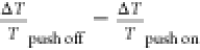 ), with its relaxation tracking the HC cooling
process. The PPP technique affords better resolution of the HC cooling
dynamics at low carrier density, whereas TA spectroscopy usually requires
a relatively large pump carrier density that may complicate the data
interpretation arising from multiband excitation and many-body effects
(particularly for perovskites). A type II structure was found at the
interface of the bilayer MAPbI3/Bphen system (Figure 18d). Meanwhile,
in the control sample without Bphen, the band-edge PB amplitude is
reduced after the arrival of a third push pulse of 2.07 eV, followed
by partial recovery of the PB amplitude within one picosecond, consistent
with reported HC cooling time under similar excitation intensities.
Comparatively with the Bphen layer present, the short-lived sharp
peak in the ΔΔT signal signifies that
HC relaxation has disappeared. This suggests that HCs with enough
excess energies can be pushed into the Bphen layer. Instead, when
the HCs possess less energy with a low push photon energy of 1.03
eV, a short-lived sharp peak in the ΔΔT signal is present for both samples, and only a negligible difference
is observed in the ΔΔT signal. This push
energy-dependent ΔΔT signal in the bilayer
and control sample indicates that there is an energy potential barrier
impeding HCs injection into the Bphen layer. Push energy-dependent
transient kinetics experiments reveal an energy potential barrier
between 1.01 and 1.08 eV above Bphen’s LUMO level (Figure 18e).
), with its relaxation tracking the HC cooling
process. The PPP technique affords better resolution of the HC cooling
dynamics at low carrier density, whereas TA spectroscopy usually requires
a relatively large pump carrier density that may complicate the data
interpretation arising from multiband excitation and many-body effects
(particularly for perovskites). A type II structure was found at the
interface of the bilayer MAPbI3/Bphen system (Figure 18d). Meanwhile,
in the control sample without Bphen, the band-edge PB amplitude is
reduced after the arrival of a third push pulse of 2.07 eV, followed
by partial recovery of the PB amplitude within one picosecond, consistent
with reported HC cooling time under similar excitation intensities.
Comparatively with the Bphen layer present, the short-lived sharp
peak in the ΔΔT signal signifies that
HC relaxation has disappeared. This suggests that HCs with enough
excess energies can be pushed into the Bphen layer. Instead, when
the HCs possess less energy with a low push photon energy of 1.03
eV, a short-lived sharp peak in the ΔΔT signal is present for both samples, and only a negligible difference
is observed in the ΔΔT signal. This push
energy-dependent ΔΔT signal in the bilayer
and control sample indicates that there is an energy potential barrier
impeding HCs injection into the Bphen layer. Push energy-dependent
transient kinetics experiments reveal an energy potential barrier
between 1.01 and 1.08 eV above Bphen’s LUMO level (Figure 18e).
Apart from the aforementioned selective extraction of HCs to the Bphen layer, fast HC transfer was also reported in the conventional cascade energy landscape in which both HCs and cold carriers were extracted to the charge transporting layer.293−295,298,299 Sarkar et al. reported HC transfer in CsPbBr3 NCs films interfaced with benzoquinone (BQ) molecules (electron acceptor) or phenothiazine (PTZ) molecules (hole acceptor) using time-resolved terahertz spectroscopy (TRTS).293 TRTS is another powerful technique that can directly differentiate whether the photoexcited carrier species are free charge carriers or excitons based on their distinct photoconductivity responses.300,301 Free electrons and holes dominate the THz photoconductivities of these samples. Meanwhile, a large quenching of the initial photoconductivity in a sub-300 fs time scale was observed when CsPbBr3 NCs films were interfaced with either BQ or PTZ charge transporting layer (Figure 18f), indicating a fast hot electron or hot hole transfer process. Significant quenching (∼90% in NC–BQ and ∼80% in NC–PTZ systems) was observed compared to neat NC films, which may be due to the Auger-assisted hole transfer to the highest occupied molecular orbital (HOMO) of BQ or ultrafast interfacial back transfer.293 Similar ultrafast quenching of THz photoconductivity was also reported by Ponseca, Jr. et al. in MAPbI3 films interfaced with a hole transporting layer of Spiro-OMeTAD (hole acceptor).299 In another study by Dursun et al., faster hot hole extraction was observed in MAPbI3/Spiro-OMeTAD compared to hot electron extraction in TiO2/MAPbI3294 (Figure 18g). There is a greater reduction of the high-energy tail in the TA spectrum (i.e., a decrease in HC temperature) for the MAPbI3–Spiro-OMeTAD sample compared to the MAPbI3–TiO2 sample (Figure 18f). This suggests a faster hot hole extraction, which was attributed to the strong overlap of the localized charge of the VB from spiro-OMeTAD with aligned delocalized electronic states on the surface of MAPbI3. However, the real interface scenario is different from the assumed MAI- or PbI2-terminated MAPbI3 (001) slab modes, which calls for more simulations for a clearer understanding. Further evidence of hot electron extraction was provided by Jiménez-López et al. in the TiO2/MAPbI3 interface using TA spectroscopy.295 The amplitude of the 780 nm sub-bandgap PIA (i.e., HC’s signature) was reduced for the MAPbI3–TiO2 sample compared to the reference (Figure 18h). The nonzero PIA suggests electron trapping at the interface because of the energy barrier. A thin C60 interlayer in between the interface helps to suppress the PIA and improve the hot electrons extraction to TiO2 (Figure 18i).
While HC extraction studies have been reported in both cascade energy landscape and interfacial energy potential barrier, these incipient investigations of HC extraction are mostly based on phenomenological studies. Detailed modeling of how this HC extraction process occurs is still lacking and further work is warranted.
5. Polaron Formation, Exciton Formation, and Dissociation
Polaron formation,14,15,17,302−304 as well as exciton formation114,305 and dissociation305,306 processes occur alongside HC cooling over similar time scales after photoexcitation. These fundamental photophysical processes can be probed using ultrafast optical techniques and theoretically modeled. In this section, we focus on distilling these ultrafast processes in HPs.
5.1. Polaron Formation
Polaron is a quasi-particle formed between a charge carrier and the associated polarization cloud of distorted surrounding ions that creates an attractive potential well. It has a profound impact on the optoelectronic properties of polarizable materials. Depending on the range and strength of the electron–phonon interaction, polarons can be generally classified as either large or small polarons.
5.1.1. Large Polarons
Large polarons are formed due to the long-range electron-LO phonon interaction in polar crystals. The Hamiltonian consisting of the electron, phonon, and electron–phonon coupling in a 3D system can be described by the Fröhlich model:307
| 28 |
with an interaction potential:
| 29 |
and a dimensionless Fröhlich coupling constant:
| 30 |
where ϵk, ĉk+, ĉk, âq, âq, ϵ∞, ϵS, ϵ0, e, m, ℏ, ωLO, and V are the eigenenergy
of the electron with wave vector k, creation and
annihilation operators for the electron, creation and annihilation
operators for LO phonons with a wave vector of q,
electric and static dielectric constants, vacuum permittivity, electric
unit, carrier effective mass, reduced Planck’s constant, LO
phonon frequency, and volume of the system, respectively. Large polarons
or Fröhlich polarons are present in polar semiconductors or
ionic crystals, including HPs. As seen from eq 30, α varies for different effective
masses, dielectric constant, as well as the LO phonon energy. Notably,
the above Fröhlich model applies to both weak and intermediate
coupling regions with 0 < α < 3 and 3 < α <
6, respectively. The large polaron with its radius  larger than the lattice constant is featured
with a coherent motion with a relatively large carrier mobility (≫
1 cm2 V–1 s–1) which
increases with decreasing temperature. Generally, as the electron
moves, the polarization of the surrounding ions and the induced lattice
distortion results in larger inertia. This leads to the polaron having
a larger mass mp ≈ m/(1 – α/6) than the mass of the underlying electron
while preserving its delocalized nature. The attractive potential
well results in a polaron binding energy Ep = −ℏωLO (α + 0.0159α2 + 0.0081α3). Due to the strong electron-LO
phonon scattering, the mobility of large polarons is often limited
(at least in certain temperature ranges) by scattering with LO phonons.
Consequently, the mobility of large polarons will be inversely proportional
to the LO phonon occupation number which increases with temperature.
larger than the lattice constant is featured
with a coherent motion with a relatively large carrier mobility (≫
1 cm2 V–1 s–1) which
increases with decreasing temperature. Generally, as the electron
moves, the polarization of the surrounding ions and the induced lattice
distortion results in larger inertia. This leads to the polaron having
a larger mass mp ≈ m/(1 – α/6) than the mass of the underlying electron
while preserving its delocalized nature. The attractive potential
well results in a polaron binding energy Ep = −ℏωLO (α + 0.0159α2 + 0.0081α3). Due to the strong electron-LO
phonon scattering, the mobility of large polarons is often limited
(at least in certain temperature ranges) by scattering with LO phonons.
Consequently, the mobility of large polarons will be inversely proportional
to the LO phonon occupation number which increases with temperature.
Large polarons have piqued the interest of the community with their far-reaching effects on the fascinating properties of HPs, such as moderate carrier mobilities, long carrier diffusion length, low carrier recombination rate, and defect tolerance, etc.11,12,225,226,308−310 The formation of large polaron (with binding energies from several to tens of meV) depends on the chemical composition and structural dimensionality as well as the ease of structural distortion of the HPs (refs (14, 16, 136, and 311−315)). Meanwhile, typical α values of 1.28–2.68 were reported in 3D lead HPs with chlorine perovskites showing the largest values, bromide perovskites with intermediate values, and iodine perovskites the smallest, suggesting different ionic metal-halide bonding strengths.251,315 Furthermore, α of lead-based 3D perovskites is larger than that of tin-based 3D perovskites but smaller than that of double perovskites.315 Despite the extensive experimental and theoretical approaches taken to scrutinize the properties of large polarons in HPs, a coherent picture is still wanting, especially on the role of organic cations,11,12,14,28,225,226,232,313,316,317 the formation mechanisms,16,226,303,304,318 polaron binding energies,11,312,313,316,319 as well as their implications on defect tolerance, moderate carrier mobility, and slow carrier recombination rate, etc.11,12,29,30,225,320,321 This is partly due to varying sample qualities, different experimental techniques and conditions as well as theoretical approaches employed. Nevertheless, there is some consensus: (1) formation of large polarons with binding energies several to tens of meV is dominated by charge carrier coupling to the inorganic octahedral vibrations in 3D lead HPs following charge carrier injection; (2) enhancement of band-edge carrier effective mass and a reduced carrier mobility following polaron formation; (3) inadequacy of the Fröhlich polaron model (with approximations of harmonic lattice potential and low-order electron–phonon coupling) to fully describe HPs band-edge carrier properties (especially transport) due to HPs soft and anharmonic lattice and associated local polar fluctuations.315,322−325 In this section, we will only focus on the ultrafast polaron formation process instead of clarifying their distinct signatures and implications on HP optoelectronic properties. Interested readers are referred to several excellent comprehensive reviews on these topics.11,225,307,314,323,326,327
Large polaron formation kinetics were first explored by X.Y. Zhu’s group using TR-OKE spectroscopy to account for the long-lived (∼100 ps) high-energy tail of the PL spectrum in hybrid bromide perovskite SCs compared to the fully inorganic CsPbBr3 SCs under low fluence photoexcitations11,21,226,232 as well as a distinct vibrational TR-OKE response upon above-bandgap photoexcitation.11,12 However, their subsequent 2D TR-OKE results showed that the latter observation turned out to be an artifact due to the polarization dressed light propagation in different crystallographic phases instead of the polaron related structure dynamics.275 Numerous studies have demonstrated that large polaron formation is dominated by the charge carriers coupling to the vibrational motion of the inorganic lattice, while the A site cation only plays a minor and indirect role by affecting the distortion of the inorganic lattice.14,31,251,310,315,328,329 Both incoherent and coherent electron–phonon coupling have been identified as fingerprints of the large polaron formation process.
Bretschneider et al. first performed a quantitative study on the ultrafast polaron formation in 3D lead iodine perovskite films with different A-site cations using optical pump-THz probe (OPTP) spectroscopy.14 From the transient photoconductivity, there is an obvious slow rise in kinetics for above-bandgap versus near-bandgap pump excitation (Figure 19a). This photoconductivity rise following on-gap photoexcitation was attributed to the reduced carrier scattering rate upon polaron formation. A cascade process of HC cooling and polaron formation is assumed. They found that polaron formation time is temperature-independent (T ≥ 160 K) and occurs with similar time scales of ∼400 fs irrespective of different A-site cations, whereas HC cooling shows both temperature and excess-energy dependences (Figure 19b). The insensitivity of polaron formation to the temperature variation was attributed to the low Debye temperature (T < 140 K) that the LO phonons with a frequency of ∼3 THz can be easily excited thermally. The observed ultrafast polaron formation was attributed to the electron coupling to the LO phonons, which is dominated by the vibrational motion of the Pb–I network, resulting in an A-site cation-independent polaron formation.
Figure 19.

(a) Early time THz photoconductivity dynamics in MAPbI3 films with different excess energies of photogenerated carriers at 160 K. The solid curves are the model fitting. (b) Fitted HC cooling time as a function of excess energies of photoexcited carriers for MAPbI3, FAPbI3, and CsPbI3 at 160 and 295 K. (a,b) Reproduced with permission from ref (14). Copyright 2018 Wiley-VCH. (c) (Top) Transient THz photoconductivity of CsPbBr3 NCs films pumped at 400 nm at delays of 3 and 100 ps. The solid curves are the curve-fits using the Drude-Lorentz model. (Bottom) Calculated electron–phonon coupling coefficients of the involved phonon modes. Reproduced with permission from ref (17). Copyright 2019 American Physical Society. (d) Transient scattering intensity of (−1 −3 2) reflection measured near the Bragg peak (green) and in the tail region (red), showing a delayed and prompt structural response, respectively. Reproduced with permission from ref (15). Copyright 2021 Nature Publishing Group. (e) Antidiagonal line width dynamics of CsPbI3 NCs (dark-blue curve) and the Kubo line shape model of typical molecular solvation (red curve). (f) Schematic of polaron formation of panel (d). (e,f) Reproduced with permission from ref (304). Copyright 2019 Nature Publishing Group. (g) Schematic of polaron formation from displaced excited state to the ground state via the emitting of coherent phonons along modes of I–Pb–I bending and stretching vibrations. Reproduced with permission from ref (318). Copyright 2018 Nature Publishing Group. (h) (Top) Normalized beating map of the reflectance spectrum. Vertical dashed line marks the LO phonon frequency at 3.7 THz. (Bottom) Calculated dielectric energy loss function describing the inelastic optical phonon scattering, and the screening function describing the renormalization of dressed charges. (i) Frequency domain of the beating map showing an onset of a coherent beat between the charge motion at ω and ωLO. (h–i) Reproduced with permission from ref (303). Copyright 2019 American Association for the Advancement of Science.
Although the slower photoconductivity rise from on-gap photoexcitation indicates large polaron formation, direct evidence of the coupling between the photoexcited charges and vibrational motion of inorganic lattice is still limited. Using OPTP spectroscopy, Cinquanta et al. addressed this gap in large polaron formation of charge carriers coupling to the distorted PbBr3 lattice in CsPbBr3 NC films.17 Instead of a pure Drude free carrier response, the transient THz photoconductivity spectrum displays a Drude–Lorentz response with contributions from both free carriers and lattice vibrations of 27, 42, and 58 cm–1 (Figure 19c). This distinct THz photoconductivity response was found to be different from that of nonpolar Si crystal,330 III–V compound GaAs,331 and 2D material MoSe2332 with the absence of phonon contribution at lower energies, indicating a much softer lead HP lattice. These phonon modes are consistent with their DFT calculations. Meanwhile, their DFT calculations showed that upon hole injection, an average shortening of the Pb–Br bond lengths is associated with an increase of the Br–Pb–Br angle of ∼10° in the PbBr6 octahedra. They proposed that the large polaron formation is dominated by the charge carrier coupling to the activated phonon modes. Furthermore, a red-shift of phonon frequency of the photoconductivity spectrum with delay time was observed, which was attributed to the softening of Pb–I lattice arising from the reduced lattice contraction by decreasing the hole population (Figure 19c).
The polaron formation associated with lattice distortion upon photoexcitation was further confirmed by Guzelturk et al. using ultrafast optical pump X-ray diffusive scattering probe measurement in MAPbBr3 SCs.15 They found that immediately after above-gap photoexcitation, in the measured transient scattering intensity of (−1 −3 2) reflection, the kinetics measured at q = 0.4 nm–1 were prompt, whereas that of q ≈ 0 is anomalously delayed by ∼20 ps (Figure 19d). The diverse onset time response for different wave vector q indicates a spatiotemporal evolution of the local lattice distortions upon photoexcitation. Meanwhile, they found that an expansive strain field was generated after photoexcitation, which resulted in both an asymmetric response with q and a sign change on opposite sides of the Bragg peak. An average strain of 0.1%, a polaron radius of 3 nm and a polaron binding energy of 10 meV were estimated. Further large polaron formation is evidenced from the TR measurements which revealed a continuous increase of the effective mass up to 20 ps after excitation with a 400 nm pump. The observed polaronic tensile lattice expansion is consistent with a recent report of 2D Cs3Bi2Br9 NCs by Wang et al. using time-resolved X-ray diffraction (XRD) spectroscopy.333 A red-shift associated with line width broadening of XRD peak indicating lattice expansion was observed after slightly above-exciton peak pump at 400 nm with a fluence of 0.6 mJ cm–2, which was mainly attributed to the increase of microstrain to ∼0.15%. Further evidence of this tensile microstrain is provided by the comparable tensile strain lifetime with that of exciton lifetime measured using PL and TA techniques. The induced tensile strain was assigned to the population of antibonding states by the electrons in the CB and depopulation of bonding states by the holes in the VB, resulting in a weakening and lengthening of Bi–Br bonds.334
Differing from the conventional Fröhlich mechanism of large polaron formation, Seiler et al. proposed an alternative polar solvation mechanism in CsPbI3 NCs analogous to that of molecular dyes in a study scrutinizing the homogeneous (antidiagonal) line width dynamics using 2DES spectroscopy.304 In this case, the polaron is formed when the charge carrier is immersed in a polar solvent, interacting with the solvent and modifying its polarization, resulting in modifications of the electronic transition and carrier mobility.335 They found that unlike covalent polar CdSe NCs whose spectral dynamics show an LO phonon induced oscillation due to relaxation within a discrete manifold of states, the spectral dynamics of CsPbI3 NCs exhibit a single rise analogous to that of a molecular dye Nile Blue that arises from the energy relaxation from polar solvation (Figure 19e). Apart from these unique spectral dynamics, they also observed an ultrafast rise followed by a decrease of the high-energy tail in the pseudo-TA spectra, where the latter was attributed to HC cooling. The spectral dynamics were modeled by a dissipative and diffusive model using the Kubo and Huang–Rhys lineshapes, which yielded a polaron formation time of ∼110 fs and a polaron binding energy of ∼50 meV (Figure 19f).
Coherent electron–optical phonon coupling is also a well-recognized fingerprint of large polaron formation in HPs.16,18,33,303,318,336−340 In this case, the impulsive launched coherent vibrational wavepackets by ultrashort laser pulse will periodically modify the electronic states, resulting in a beating map, which is usually superimposed on the carrier population related response. Typically, the polaron formation process is completed when the coherent lattice vibrations end. Hence, the dephasing time of coherent lattice vibrations can be approximated as the polaron formation time provided that the effects of scattering from phonon–phonon interactions and defects are negligible. Nevertheless, observation of coherent lattice vibrations requires that the activated phonon modes are Raman active and possess longer vibrational periods than the laser pulse duration such that only contributions from these undamped phonon modes to the polaron formation can be detected. Such a study of coherent electron–phonon coupling was first reported by Ghosh et al. in MAPbI3 and MAPbBr3 films using impulsive vibrational spectroscopy based on the TA technique.336 A displaced harmonic oscillator model was employed to estimate the electron–phonon coupling strengths. Large polaron formation was concluded from the estimated Huang–Rhys factors of the activated LO phonon modes, which were much smaller than unity.
Another evidence of the ultrafast large polaron formation process was provided by Batignani et al. in MAPbBr3 films using TA spectroscopy.33 By comparing the coherent optical phonon induced beating maps in the PB region under resonant and nonresonant photoexcitations, they identified that two phonon modes of 89 and 106 cm–1 were coupled with excited electronic states. These two phonon modes were launched by the displacive excitation process and were identified solely upon resonant photoexcitation that dominated the polaron formation process. The polaron formation time was approximated as the phonon lifetime of ∼1 ps. A similar ultrafast polaron formation process was also probed by Park et al. in MAPbI3 films using TA spectroscopy with an above-bandgap pump.318 However, rather than comparing the activated phonon modes under resonant and off-resonant pump energies, they examined the coherent electron–phonon coupling by detecting the coherent vibrational wavepackets induced beating map on the excited states induced absorption in the TA spectrum. Three phonon modes of ∼20, ∼ 43, and ∼75 cm–1, corresponding to the skeletal bending, in-plane bending, and c-axis stretching of PbI6 octahedral vibrations were, respectively, identified to be coupled with the excited electronic states. Two phonon modes of ∼20 and ∼75 cm–1 were found to dominate the relaxation of the excited polaron state to the charged-state minimum with a reorganization energy of 145 meV (Figure 19g). Likewise, ultrafast large polaron formation was also reported in 2D HPs (such as (PEA)2PbI4,16,18 (HA)2PbI4,18,337 and (BA)2PbI416,337) using TA spectroscopy via monitoring modulation of electronic state transitions by coherent optical phonons upon photoexcitation. These results show that the coherent lattice vibrations involved in the large polaron formation process are dominated by the phonon modes from the inorganic lattice with the A-site cation playing a minor role.
Other than probing the electronic state transitions, ultrafast
polaron formation can also be detected from the coherent phonons modulated
transient THz photoconductivity of excited carriers.303 Using ultrafast OPTP spectroscopy, Lan et al. found that contrasting with electronic states modulation which shows
a 1π phase shift around the transition resonance, the coherent
LO phonon-induced beating map in transient THz reflectivity of MAPbI3 SCs at resonant pump displayed a dispersive feature with
both the oscillation frequency and amplitude depending on the probe
frequency (Figure 19h,i).303 Considering that the carrier-optical
phonon interaction is governed by a dressed Coulomb interaction,  that is modified through dynamic screening
of the lattice dielectric function ϵ(ω, τ), the
sign change in the observed beating map can thus be attributed to
the transition from an overscreened to an under-screened lattice response,
where the lattice polarization moves from an in-phase to an out-of-phase
response to the electromagnetic perturbation.341 Further analysis of the transient THz reflectivity dynamics
revealed that the polaron formation time is comparable to the coherent
phonon dephasing time both of which first decreased with increasing
probe frequency and then reduced to a constant for probe frequency
above 5 THz. Large polaron formation is confirmed from the estimated
polaron binding energy of 30 meV and the polaron radius of 3.5 nm
that is around six unit cells. Another evidence of ultrafast large
polaron formation can be seen from the THz emission kinetics of MAPbI3 films upon above-bandgap photoexcitation. Guzelturk et al. found that the THz emission kinetics displayed coherent
LO phonons (∼40 and ∼92 cm–1) induced
oscillations that persisted for several picoseconds in addition to
that due to the photo-Dember effect (i.e., charge
dipole formation near the surface upon ultrafast photocarrier generation).342
that is modified through dynamic screening
of the lattice dielectric function ϵ(ω, τ), the
sign change in the observed beating map can thus be attributed to
the transition from an overscreened to an under-screened lattice response,
where the lattice polarization moves from an in-phase to an out-of-phase
response to the electromagnetic perturbation.341 Further analysis of the transient THz reflectivity dynamics
revealed that the polaron formation time is comparable to the coherent
phonon dephasing time both of which first decreased with increasing
probe frequency and then reduced to a constant for probe frequency
above 5 THz. Large polaron formation is confirmed from the estimated
polaron binding energy of 30 meV and the polaron radius of 3.5 nm
that is around six unit cells. Another evidence of ultrafast large
polaron formation can be seen from the THz emission kinetics of MAPbI3 films upon above-bandgap photoexcitation. Guzelturk et al. found that the THz emission kinetics displayed coherent
LO phonons (∼40 and ∼92 cm–1) induced
oscillations that persisted for several picoseconds in addition to
that due to the photo-Dember effect (i.e., charge
dipole formation near the surface upon ultrafast photocarrier generation).342
5.1.2. Small Polarons
Distinct from large polarons, small polarons are formed because of strong and short-range electron–phonon interactions. The Hamiltonian of the system can be generally described by the Holstein model:307
| 31 |
where g is the coupling constant, N is the total number of unit cells, and ℏω0 is the coupled phonon energy. The small polarons with
their wave functions strongly localized within the lattice constant
are widely present in a variety of materials, including transitional-metal
oxides,326,343−346 amorphous materials,347−349 polymers,349−351 alkali halides,352,353 and the low-dimensional HPs.59,354−356 The small polaron is characterized by the incoherent phonon-assisted
thermal hopping motion with a much smaller carrier mobility (≪
1 cm2 V–1 s–1) which
increases with temperature.307 In the case
of strong electron–LO phonon coupling induced small polarons,
one can obtain the polaron binding energy 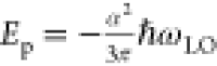 and polaron effective mass mp ≈ 0.0202α4.357 Due to the robust carrier localization and
local lattice distortion effects arising from the strong electron–phonon
interactions, small polarons strongly bind to carriers and are thus
also known as intrinsically self-trapped states. On the other hand,
these strong electron–phonon interactions broaden the electronic
transitions substantially, usually leading to a broad low-energy tail
in the emission spectrum. This can be understood based on a simple
configuration coordination model in which the line shape of the emission
spectrum is significantly broadened by the strong electron–phonon
scattering (Figure 20a). Similarly, this electron–phonon interaction will also
broaden the absorption spectrum considering that light absorption
is an inverse process of light emission.
and polaron effective mass mp ≈ 0.0202α4.357 Due to the robust carrier localization and
local lattice distortion effects arising from the strong electron–phonon
interactions, small polarons strongly bind to carriers and are thus
also known as intrinsically self-trapped states. On the other hand,
these strong electron–phonon interactions broaden the electronic
transitions substantially, usually leading to a broad low-energy tail
in the emission spectrum. This can be understood based on a simple
configuration coordination model in which the line shape of the emission
spectrum is significantly broadened by the strong electron–phonon
scattering (Figure 20a). Similarly, this electron–phonon interaction will also
broaden the absorption spectrum considering that light absorption
is an inverse process of light emission.
Figure 20.

(a) Schematic of the configuration coordination model showing the formation and relaxation of self-trapped states due to strong electron–phonon interaction. Phonons are emitted in the process from A to C (absorption) and C to A (emission) which broaden the absorption and emission spectra, respectively. The red curve shows the self-trapping process. (b) TA spectrum of Cs2AgSb0.25Bi0.75Br6 colloidal NCs pumped at 360 nm. The TA spectrum consists of a PB band and a broad below-bandgap PIA band. (c) Exciton PB kinetics at different ⟨N⟩ which shows two fast decay lifetimes (i.e., τ1 and τ2) and one long lifetime (i.e., τ3) attributed to the many-body Auger interaction. Here, τ1 and τ2 were attributed to exciton self-trapping because of small polaron formation and surface traps, respectively. (b,c) Reproduced with permission from ref (358). Copyright 2019 Wiley-VCH. (d) TR kinetics of Cs2AgBiBr6 SC probed near the direct exciton resonance at 440 nm. (e) TR kinetics probed near the isochromatic point (∼2.83 eV) showing the oscillation contributed by coherent optical and acoustic phonon modes. (d,e) Reproduced with permission from ref (302). Copyright 2021 American Association for the Advancement of Science.
Experimentally, the strength of this short-range electron–phonon interaction can be evaluated from the Urbach-tail of the absorption spectrum, which gives rise to359
| 32 |
with Urbach energy EU = kBT/σ, where σ = 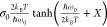 is the constant,
  is the high-temperature limit of σ, s is a dimensionless parameter that is determined only by
the dimensionality and the lattice geometry, B is
the exciton band halfwidth, ELR is the
lattice relaxation energy, and X is related to extrinsic
factors such as defects or lattice strain. Typically, s is 1.5 for a simple cubic lattice and 1.24 for a square lattice.
As shown, the lower the temperature, the smaller the σ and the
larger the EU and, thus, the easier the
carrier trapping. The electron–phonon coupling constant is
then obtained as
is the high-temperature limit of σ, s is a dimensionless parameter that is determined only by
the dimensionality and the lattice geometry, B is
the exciton band halfwidth, ELR is the
lattice relaxation energy, and X is related to extrinsic
factors such as defects or lattice strain. Typically, s is 1.5 for a simple cubic lattice and 1.24 for a square lattice.
As shown, the lower the temperature, the smaller the σ and the
larger the EU and, thus, the easier the
carrier trapping. The electron–phonon coupling constant is
then obtained as  . For self-trapping to occur, it generally
requires g ≥ 0.92 (i.e.,
σ0 ≤ 1.63) for the 3D case and g ≤ 0.87 (i.e., σ0 ≤
1.43) for the 2D case.
. For self-trapping to occur, it generally
requires g ≥ 0.92 (i.e.,
σ0 ≤ 1.63) for the 3D case and g ≤ 0.87 (i.e., σ0 ≤
1.43) for the 2D case.
Analogous to large polaron formation, small polaron formation also depends on the chemical composition, lattice distortion, and crystal dimensionalities.31,55,136,311,314,319,360−362 Small polarons mostly manifest as self-trapped excitons (STEs) in low-dimensional HPs and double perovskites.55,354,362−364 This is because, for 3D lead HPs, g lies in the range of 0.6–0.88 and, thus, no STEs are formed.365,366 In contrast, g values of 70–120 in 0D lead HPs,290,367,368 0.98–3.8 in 2D lead HPs,369−371 2.8–70 in bismuth double perovskites,372−374 0.83–2.3 in CsPbBr3 nanoplatelets295,356,375,376 indicate the increased likelihood of small polarons. However, precise determination of σ0 is obfuscated by extrinsic defects/disorders in the sample, which also leads to the exciton self-trapping and a low-energy tail in the absorption or emission spectra,360,377,378 thus affecting the estimation of EU. Hence, due care must be taken when estimating the intrinsic electron–phonon coupling constant g based on the Urbach-tail in the absorption spectrum. While there has been several experimental and theoretical reports on the small polarons in HPs, most of them mainly focused on the broad emission features as well as fine-tuning of the STEs.295,356,364,370,374−376,379−384 Studies on the ultrafast small polaron formation process are few and far between. Nevertheless, elucidating all these features is beyond the scope of this review. Hence, we will focus on the fundamental physical process of ultrafast small polaron formation or exciton self-trapping in several typical HPs for the remainder of this section.
Yang et al. provided the first report on the small
polaron-induced exciton self-trapping in lead-free double perovskite
Cs2AgSb1–yBiyX6 (X: Br, Cl; 0 ≤ y ≤ 1) NCs using TA spectroscopy.358 They verified the presence of STEs based on (1) a broad below-bandgap
PIA band in the TA spectrum (Figure 20b); (2) a broad below-bandgap PL centered at ∼610
nm at 77 K; (3) an ultrafast decay of PB kinetics over 1–2
ps (i.e., τ1) that is present at
both very low and high pump fluences but is not affected by the presence
or absence of capping ligands, which can change the trap density and
thus affect the surface defects-mediated PB decay kinetics (i.e., τ2) (Figure 20c). The electron–phonon coupling
strength was then extracted from the temperature-dependent PL line
width of this STE emission using the model from ref (251), which yielded the electron–acoustic
phonon coupling strength γac ∼ 0.03 eV and
electron–LO phonon coupling strength γLO ∼
0.96 eV. The electron–LO phonon coupling strength is over 1
order of magnitude larger than that of 3D lead HPs (γLO ∼ 0.04–0.06 eV),251 which
is believed to result in the ultrafast small formation of STEs. These
STEs are likely located in two neighboring octahedra (AgBr6 and BiBr6) with the hole contributed by the Ag 4d/Br
4p orbitals and the electron by Bi 5s/Br 4p orbitals, similar to that
of Cs2AgInCl6.385 Nevertheless, the carrier scattering induced PL line width broadening
model may not apply to STEs given that the Fröhlich interaction
model is inapplicable to the strong electron–phonon coupling
of small polarons. A more rigorous model is given by the theory of
Toyozawa,386 which models the PL line width
as379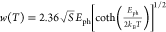 , where Eph is
the average phonon energy and S is the Huang–Rhys
factor. Similar ultrafast exciton self-trapping with subpicosecond
polaron formation was reported in 1D perovskite [DMEDA]PbBr4,387 Sb-doped Rb3BiCl6,388 and 0D perovskite Cs4PbX660 probed using TA spectroscopy
and recently in vacancy-ordered lead-free perovskite Cs3Bi2Br9389 by ultrafast
X-ray TA spectroscopy.
, where Eph is
the average phonon energy and S is the Huang–Rhys
factor. Similar ultrafast exciton self-trapping with subpicosecond
polaron formation was reported in 1D perovskite [DMEDA]PbBr4,387 Sb-doped Rb3BiCl6,388 and 0D perovskite Cs4PbX660 probed using TA spectroscopy
and recently in vacancy-ordered lead-free perovskite Cs3Bi2Br9389 by ultrafast
X-ray TA spectroscopy.
Though ultrafast carrier self-trapping due to small polaron formation has been observed, explicit experimental evidence of this electron–phonon scattering process remains lacking. Our group provided direct evidence of this electron–phonon coupling induced ultrafast exciton self-trapping process in bismuth-based double perovskite Cs2AgBiBr6 SCs using TR and OPTP spectroscopies.302 From the temperature-dependent PL line width, we found that the photoexcited carriers are coupled to both acoustic phonons and optical phonons, consistent with the broad PL line width at room temperature. Meanwhile, the band-edge TR decay kinetics showed three lifetimes with contributions from HC cooling by Fröhlich interaction (∼0.25 ps), ultrafast carrier trapping by acoustic phonons (∼4.7 ps), and slow carrier trapping by defects (∼49 ps) (Figure 20d). The ultrafast and slow carrier trapping processes were validated by fluence-dependent OPTP measurements. Further studies on the coherent lattice vibrations with the beating map near the isochromatic point (∼2.83 eV) contributed by both coherent optical phonons (∼5.3 THz) and acoustic phonons (∼0.2 THz) indicated that both optical and acoustic phonons were involved in the ultrafast carrier trapping process (Figure 20e). This phonon-assisted small polaron formation associated with carrier self-trapping is similar to that of large polaron formation, as mentioned previously.390 On the other hand, compared to the Fröhlich interaction mechanism, which showed similar coupling strengths to that of the 3D perovskite CsPbBr3, this double perovskite possesses a much larger total deformation potential constant of 21.2 eV with coupling constant g ∼ 1 for both electron and holes. We proposed that the charge carriers are first localized by the optical phonons via Fröhlich interactions but are later trapped by interacting with acoustic phonons via deformation potential interactions. The small polaron formation associated with drastically reduced carrier mobility indicates that this family of Bi-based double perovskites may not be a good candidate in photovoltaics. Nonetheless, there remain some knowledge gaps in the small polaron picture. For instance, it is still unclear why the formation of STEs occurs at carrier densities larger than 1017 cm–3. More studies are needed to fully understand the Bi-based double perovskite system for applications.
5.2. Exciton Formation and Dissociation
Excitons are electron–hole pairs bound by Coulomb interactions as described in section 2.3. Understanding the processes of exciton formation and dissociation into unbound charges along with their interactions with phonons is crucial to understanding and controlling optical properties since these processes directly influence the recombination dynamics at later time scales. The ultrafast dynamics in the first few picoseconds after photoexcitation involves the interplay of excitons, free charges, and lattice vibrations or phonons. In semiconductors, excitons are of two classes based on their genesis: geminate versus non-geminate excitons. Geminate excitons are directly formed from photoexcitation, while indirect formation from thermalized electrons and holes yields non-geminate excitons. The formation of geminate excitons is schematically shown in Figure 21a,b. When the material is excited by an above-gap photon, free carriers with excess energy are generated along with a small proportion of geminate excitons. The formation of geminate excitons, as shown in Figure 21a, is indirect and limited due to the additional momentum requirement for coupling to phonons. As free carriers relax to the band-edge, non-geminate excitons are formed depending on factors such as exciton binding energy and carrier screening. In the second case shown in Figure 21b, geminate excitons with zero momentum are directly generated with resonant photoexcitation. In this section, we will first discuss the dynamics of exciton formation and dissociation in HPs revealed via experiments that directly probe the ultrafast process. Next, we will focus on the factors that influence exciton dissociation and reports of secondary exciton formation.
Figure 21.

Schematic energy (E)-momentum (K) dispersion curves showing geminate exciton formation in HPs for above-gap (a) and resonant (b) photoexcitation. In panel (a), free electrons and holes as well as a minority of geminate excitons are generated due to additional momentum conservation requirements. In panel (b), geminate excitons with zero momentum are generated resonantly. Here, K is the total momentum of the electron and hole pair to show the exciton (solid black curve) and free carrier states (green shade) in the same schematic. The red arrow indicates photoexcitation of carriers, and the brown curly arrow indicates the scattering of free charges with phonons. (c) Time-resolved THz reflectance spectrum of MAPbI3 SCs. The peak at 12 meV is assigned to transition between 1s and 2p exciton levels. Reproduced with permission from ref (115). Copyright 2015 The Royal Society of Chemistry. Dynamics of differential conductivity obtained by THz spectroscopy for resonant (d) and nonresonant (e) photoexcitation. The shaded circles indicate the differences in transitions among exciton levels, showing changes in exciton formation dynamics. (d,e) Reproduced with permission from ref (114). Copyright 2017 Nature Publishing Group. Calculated free carrier fraction as a function of total excitation density using the Saha equation (i.e., eq 33) in representative 3D (f) and 2D (g) HPs with different exciton binding energies. (f,g) Reproduced with permission from ref (136). Copyright 2021 AIP Publishing.
Ultrafast optical spectroscopy can probe the relaxation dynamics of carriers but has the limitation of not being able to distinguish the optical response of free charges and excitons. TRTS provides a solution to directly probe phonons and intraband transitions among free carrier continuum and between excitonic states. In TRTS, a strong pulse in the visible region generates charges in the material, and a terahertz pulse is employed as the probe. The terahertz response depends on the carrier concentration and conductivity. In contrast to free electrons and holes, excitons are charge-neutral and do not contribute to the conductivity. Hence free charge and exciton responses can be differentiated using THz experiments.
A rising terahertz response signal could be attributed to the generation of free carriers from excitons. Ponseca, Jr. et al. performed a series of time-resolved experiments including TRTS on MAPbI3 films at room temperature.391 They showed a 2 ps rise time in the THz dynamics which was ascribed to the dissociation of non-geminate excitons. One of the first reported direct signatures of exciton dissociation is a study on single MAPbI3 crystals by Valverde-Chávez et al.(115) With the use of broadband THz probe pulses, a reflectance feature at 12 meV was observed in the spectrum (Figure 21c). The feature was assigned to the 1s-2p exciton transition and had a short lifetime of about 1 ps, reflecting the exciton dissociation. These reports showed the prominence of the exciton dissociation process in the early dynamics of HPs. To gain more insights into the exciton formation, Luo et al. performed TRTS experiments at 8 K temperatures and measured the transitions between excitonic Rydberg states in HPs.114 After directly pumping the excitonic state, they resolved a two-step exciton formation process with direct formation of mostly 1s excitons. This includes the loss of exciton coherence within 1 ps and the phonon scattering of the 1s excitons with finite momenta within a few picoseconds. The measured THz conductivity and exciton dynamics are shown in Figure 21d. This process is much faster at higher temperatures, as expected from the higher phonon scattering. The formation of non-geminate excitons at 8 K was observed to be even slower in the order of tens of picoseconds due to the slow cooling of HCs (Figure 21e). Zhao et al. used TRTS to study exciton dissociation in a mixed-cation 3D HP film by analyzing changes in phonon and carrier distributions in the first few picoseconds.305 From the observed anticorrelation between the spectral weights of carriers and phonons at 15 K, they clarified the interplay of exciton formation and dissociation. The presence of a large free carrier density can also enhance exciton dissociation due to free carrier Coulomb screening. Other extrinsic factors apart from carrier screening could also affect exciton dissociation. For instance, in 2D HPs, even though excitons are strongly bound, their dissociation could be greatly facilitated by layer edge states.392,393 Hence, both exciton formation and dissociation processes in HPs occur on a time scale of a few picoseconds. The latter is however affected by the exciton binding energy Eb. For instance, in 2D HPs, strongly bound excitons remain mostly undissociated as long as screening effects are not considerable.394
The balance of free carriers and excitons dictates the properties of the HPs including luminescence and conductivity. The Saha equation is commonly employed to determine the ratio of densities of free charges nf and excitons nx. For a d-dimensional semiconductor, the relation is given by the following:
| 33 |
where the branching ratio is x = nf/ntotal, ntotal = nf + nx, and the exciton reduced mass μ = memh/(me + mh). Eb and T are the exciton binding energy and temperature, respectively. This relation expresses the chemical equilibrium between exciton dissociation and formation. Figure 21f,g shows the branching ratio from the Saha equation plotted for 3D and 2D semiconductors with different Eb. D’Innocenzo et al. showed that in 3D HPs, only a negligible proportion of excitons are present at conditions relevant for practical device applications.395
The Saha equation has exhibited varying success in describing the excited state dynamics in HPs. Sheng et al. estimated the ratio of excitons to free charges to be 1:10 in MAPbI3 while also showing that when Eb is increased, the balance shifted more toward excitons.396 This ratio is higher than that predicted by the Saha equation. By exploiting the high frequency and time resolution afforded by 2DES, Jha et al. demonstrated well-resolved free carrier and excitonic transitions at room temperature in MAPbI3.397 This provided further concrete evidence that excitons coexisted with free carriers at ambient conditions. Sarritzu et al. showed using TRPL experiments that excitons dominated light absorption and emission processes in 3D HPs at low excitation densities, even though they formed the minority.398 Additionally, at low temperatures they reported an excitation density-dependent crossover in PL characteristics that seem to be at odds with predictions of the Saha equation. The PL at low carrier density is dominated by geminate excitons, which cross over to free carrier-dominated PL and then to secondary exciton-dominated PL. Later findings by Mariano et al. showed that secondary exciton formation is influenced by nonradiative trap states.399 Therefore, extrinsic parameters such as trapping could be key factors to consider while interpreting carrier dynamics using the Saha equation.
For 2D HPs with higher Eb, the Saha equation also predicts free carriers to dominate over excitons even at Eb on the order of 200 meV at ntotal relevant for devices (∼1010 cm–2, Figure 21g).136,400 In contrast, several reports suggest that excitons constitute the primary photoexcitation.394,401 Curiously, for the case of RP-phase 2D HPs of layer number n > 1, the free carriers form a majority over excitons.400 There are only limited studies on the validity of the Saha equation in the context of n > 1 RP-phase HPs. Though some existing reports indicate an efficient exciton dissociation process in these materials, the mechanism commonly attributed to layer edge-states,393 traps,402 and formation of exciton-polarons leads to screening effects306,403 rather than an intrinsic exciton dissociation.
To conclude, free carriers and excitons can coexist in HPs. Their roles in radiative and nonradiative recombination are distinct, and their respective populations depend on factors such as exciton binding energy, carrier concentration, temperature, and carrier trapping. The Saha equation, which is originally used to describe the ionization of gases in stellar environments,404 has found limited success in describing the balance between free carriers and excitons. This equation considers the chemical equilibrium of an isolated system of reactants and products. Applying this framework to HPs implies extending it to free carriers and excitons while neglecting the extrinsic influences of traps and Coulomb screening. This warrants a more detailed investigation into the branching ratios in HPs, especially for quasi-2D HPs.
6. Light-Induced Lattice Expansion and Vibration
Light-induced structural modifications, such as lattice expansion and vibration, are an important aspect of light–matter interactions that can significantly impact the optical and electronic properties of HPs. This is due to the soft lattice nature of HPs, as well as dynamic structural fluctuations that can modify the local band structure. In this section, we distill the recent reports on light-induced lattice expansion and vibration in HPs after femtosecond laser pulse excitation.
6.1. Light-Induced Lattice Expansion
Apart from the direct electronic response from photoexcited carriers and the associated polaron effect, light can also induce significant effects on the structural properties of the excited lattice. The ultrafast light-induced structural modification can usually be detected either directly using time-resolved X-ray and electron diffraction spectroscopy based on the nuclear response or indirectly with optical methods based on the dipole-allowed electronic transitions. Nevertheless, direct probe of light-induced structural modifications in HPs has only been reported lately, which may be due to the stringent requirement of high-quality HP samples that have been successfully fabricated recently.
For any significant structural modification to be detected, relatively high pump fluence is typically needed. A straightforward effect is lattice thermal expansion induced tensile strain which may affect structural, electronic, optical, as well as the long-term stability of HPs.334,405−408 This is because the whole lattice is heated up after HC cooling. Such light-induced heating effect is especially significant for soft HPs which possess relatively low thermal conductivities.409 In particular, it has been theoretically demonstrated that the light-induced lattice expansion can increase the bandgap, extend the carrier recombination lifetime, and accelerate the electronic dephasing of lead iodide perovskites.405,407 The bandgap increase due to lattice expansion-induced tensile strain was attributed to the distortion of the Pb–I network with longer Pb–I bonds and the reduced tilting of PbI6 octahedra. The carrier recombination lifetime increase was assigned to the dominant contribution from the reduction in electronic transition dephasing time that increases the carrier lifetime over that from enhanced nonadiabatic electron–phonon coupling that reduces the carrier lifetime.405,407
Depending on the time resolution of the experimental technique, the resulting lattice expansion magnitude as well as the resultant modification of the optical and electronic properties will be different. In this section, we focus on the ultrafast light-induced lattice expansion process after femtosecond laser pulse excitation. Assuming that all the excess energies of the photoexcited carriers are transferred to the lattice, the initial lattice temperature increase ΔTL along the direction of the incident pump can be approximated as
| 34 |
where R, P, α, Cv, ℏω, Eg are the reflectance, pump power,
linear absorption coefficient, volumetric specific heat, pump energy,
and bandgap, respectively. The resultant tensile strain can thus be
estimated as  , where β is the linear thermal expansion
coefficient.
, where β is the linear thermal expansion
coefficient.
The first observation of ultrafast light-induced
lattice expansion
was reported by Wu et al. in MAPbI3 films
using ultrafast electron diffraction spectroscopy.410 The signature of light-induced lattice expansion is evident
from the reduced diffraction intensity of Bragg peaks (i.e., negative transient electron diffraction signal) due to heat induced
Debye–Waller effect (Figure 22a) which gives rise to  , where ⟨uRMS2(t)⟩ is the time-dependent mean square displacement of the atoms.
The lattice expansion time was estimated to be 10 ps. This lattice
expansion corroborates well with the atoms’ mean square displacement
calculated using molecular dynamics simulations. The light-induced
heat is mainly generated by HC cooling, as evident from the negligible
transient electron diffraction signal with resonant bandgap excitation
(Figure 22b). Apart
from the lattice expansion effect, they also identified an additional
slow rotational disordering process from I atoms at the PbI6 octahedron that leads to a slight deviation of the I–Pb–I
bond angle. Their molecular dynamics simulations also show that the
isotropic light-induced heating effect alone cannot explain this structural
deformation with the differential pair distribution function (PDF)
only present for above-bandgap photoexcitation and the dynamics proceeds
faster at higher pump power (Figure 22c). Nevertheless, the exact origin of the observed
rotational distortion remains unknown, which calls for further studies.
Similar light-induced lattice expansion on a time scale of ∼5
ps was also recently reported by Zhang et al. in
monocrystalline 2D HPs SCs probed using ultrafast momentum-resolved
electron diffraction spectroscopy.411 The
lattice heating-induced Debye–Waller effect was found to give
rise to the negative transient electron diffraction in the higher-order
Bragg peaks. Other than this heating-induced lattice expansion, they
also revealed an exceptional ultrafast polaron formation process (≤1
ps), which leads to a collective lattice reordering in DJ perovskites.
, where ⟨uRMS2(t)⟩ is the time-dependent mean square displacement of the atoms.
The lattice expansion time was estimated to be 10 ps. This lattice
expansion corroborates well with the atoms’ mean square displacement
calculated using molecular dynamics simulations. The light-induced
heat is mainly generated by HC cooling, as evident from the negligible
transient electron diffraction signal with resonant bandgap excitation
(Figure 22b). Apart
from the lattice expansion effect, they also identified an additional
slow rotational disordering process from I atoms at the PbI6 octahedron that leads to a slight deviation of the I–Pb–I
bond angle. Their molecular dynamics simulations also show that the
isotropic light-induced heating effect alone cannot explain this structural
deformation with the differential pair distribution function (PDF)
only present for above-bandgap photoexcitation and the dynamics proceeds
faster at higher pump power (Figure 22c). Nevertheless, the exact origin of the observed
rotational distortion remains unknown, which calls for further studies.
Similar light-induced lattice expansion on a time scale of ∼5
ps was also recently reported by Zhang et al. in
monocrystalline 2D HPs SCs probed using ultrafast momentum-resolved
electron diffraction spectroscopy.411 The
lattice heating-induced Debye–Waller effect was found to give
rise to the negative transient electron diffraction in the higher-order
Bragg peaks. Other than this heating-induced lattice expansion, they
also revealed an exceptional ultrafast polaron formation process (≤1
ps), which leads to a collective lattice reordering in DJ perovskites.
Figure 22.

(a) Transient electron diffraction intensities of several Bragg peaks for MAPbI3 films which were excited at 400 nm with a carrier density of 2.3 × 1019 cm–3. Solid curves are global fits. (b) Transient electron diffraction signal of Bragg peak 7 for 400 and 700 nm with similar carrier density. (c) Differential pair distribution function (PDF) with the carrier density of 4.5 × 1019 cm–3 at several delay time and the simulated results that include additional fluctuation of iodine atoms. The inset is the PDF dynamics at two different carrier densities. Reproduced with permission from ref (410). Copyright 2017 American Association for the Advancement of Science.
6.2. Light-Induced Lattice Vibration
Lattice vibrations or phonons are important attributes that have significant impact on perovskites’ optoelectronic properties, especially their luminescence, carrier relaxation dynamics, thermal conductivities, carrier mobilities, etc. A good understanding of the vibrational properties of solids will hence lay solid foundations for fine-tuning the functionalities of HP devices. Collective lattice vibration dynamics are typically investigated using time-resolved X-ray scattering, electron diffraction, and optical methods, etc. which probes the modified structural, electronic, or optical properties. Among these time-resolved methods, only optical methods such as TA, TR, 2DES, transient grating, and four-wave mixing (FWM) spectroscopy have been reported with the resultant spectroscopy usually termed coherent phonon spectroscopy, which is obtained by subtracting the nonoscillatory components. Such coherent phonon spectroscopy involves the initial generation of coherent phonons by light–matter interaction as the driving force using a short laser pulse and subsequent detection of their dynamics by monitoring the induced transient grating due to refractive index modulations with a time-delayed probe pulse. Both coherent optical phonon (COP) and coherent longitudinal acoustic phonon (CLAP) dynamics have been widely reported in HPs, which we will review separately in the following subsections.
6.2.1. Coherent Optical Phonon Dynamics
COP dynamics are well-studied for both 3D (refs (32, 33, 318, 336, 338−340, and 412−415)) and 2D (refs (16, 18, 321, 337, 414, 416, and 417)) HPs and have been most recently extended into 1D418,419 HPs. A trove of physical insights into electron–phonon coupling, polaron formation, electronic states modulation, and inorganic–organic sublattice coupling, etc. has been uncovered. Here, “3D, 2D, and 1D” refer to the structural dimension rather than the spatial dimension. Considering that most studies focused on 3D and 2D HPs which are broadly similar to 1D HPs, we will concentrate on the COP dynamics in 3D and 2D HPs, examining their generation and detection mechanisms, phonon modes assignment, as well as the physical insights.
6.2.1.1. Coherent Optical Phonon Generation
Coherent optical lattice vibrations can be described by a classical damped oscillator function:
| 35 |
where μ is the lattice mass, Q is the lattice displacement, Γ is the damping constant that is related to the dephasing of the coherent phonon, and ω0 is the natural vibrational frequency. Note that eq 35 is only a phenomenological description of the coherent phonon generation process. A more theoretical treatment can be found here.420Eq 35 can be solved using inverse Fourier transform:
| 36 |
where Q(ω) and F(ω) are the Fourier transformed displacement and driving force, respectively. The solution to eq 36 can be derived using Green’s function. As seen, the mechanism of COP generation highly depends on the nature of the driving force after photoexcitation. Several mechanisms have been proposed: impulsive stimulated Raman scattering (ISRS),274,421 displacive excitation of coherent phonons (DECP),422−424 ultrafast screening of electric field in the surface-space-charge region,425,426 and nonlinear ionic Raman scattering (IRS).427−429
The first three mechanisms apply to electronic excitations
with visible to near-infrared pump frequencies while the last applies
to resonant phonon pumping using mid-infrared or THz pump frequencies.
For ISRS (Figure 23a) with below bandgap pumping, the lattice vibrations in the ground
electronic state of the material are initiated by the dipolar interactions
between the phonon modes and the ultrashort pump pulse. The magnitude
of the driving force and the resultant coherent vibration amplitude
scales linearly with pump intensity and light-scattering differential
polarizability induced by the activated phonons. Typically, ISRS occurs
through mixing among the continuous distribution of Fourier components
within the spectral bandwidth of the ultrafast laser pulse.420 The activated phonon mode can either be the
acoustic or optical mode. The presence of ISRS mandates a Raman-active
mode and a sufficiently short laser pulse duration compared to the
vibrational oscillation period. The driving force is  , where χ is linear susceptibility
and E is the laser electric field. The solution to eq 36 for the ground-state
ISRS can be expressed as274
, where χ is linear susceptibility
and E is the laser electric field. The solution to eq 36 for the ground-state
ISRS can be expressed as274
| 37 |
where  is the pump intensity, A is the electric field amplitude, n is the refractive
index,
is the pump intensity, A is the electric field amplitude, n is the refractive
index,  , c is the vacuum speed
of light, and τL is the laser pulse duration.
, c is the vacuum speed
of light, and τL is the laser pulse duration.
Figure 23.

Schematic of COP generation mechanisms. (a) Impulsive stimulated Raman scattering (ISRS), (b) displacive excitation of coherent phonons (DECP), and (c) ultrafast screening of surface depletion electric field. (c) Reproduced with permission from from ref (426). Copyright 1992 Springer-Verlag. (d) Nonlinear ionic Raman scattering (IRS) process. The red, magenta, and olive patterns correspond to the phonon manifolds of the material, pump laser profile, and induced COP profile, respectively.
For resonant ISRS with above-bandgap photoexcitation, the solution to eq 36 is given as18,430
| 38 |
where  , Ξ is the deformation potential constant,
and εR and εRlm are the real and
imaginary parts of the dielectric constant, respectively. Generally,
, Ξ is the deformation potential constant,
and εR and εRlm are the real and
imaginary parts of the dielectric constant, respectively. Generally,  , and eq 38 then becomes18
| 39 |
For DECP (Figure 23b), the lattice vibrations are initiated by the sudden increase of photoexcited carriers which creates a new equilibrium position, resulting in the displacement of the atoms’ orientations with A1 symmetry around this new position.422 This can only occur in materials with low crystal symmetry and only the A1 or A1g mode with inversion symmetry will be launched.424 Similar to ISRS, DECP also requires the laser pulse duration to be short compared to the excited-state vibrational period. The solution to eq 36 is given as422
| 40 |
where β is the carrier recombination coefficient and A is a prefactor related to the pump intensity and the Raman cross-section.
For the Coulomb screening effect, the photoexcited charge carriers give rise to ultrafast longitudinal depolarization of the depletion field at the sample surface, which initiates the coherent lattice vibration of longitudinal optical phonons (Figure 23c).425,426 In this mechanism, the lattice vibrational amplitude scales linearly with the variation of the surface depletion field, and the screening of the surface depletion field must take place fast enough, which depends on the photoexcited carrier density to initiate the lattice vibration. It was first reported as a coherent LO phonon phenomenon in bulk GaAs.425 In this case, the driving force is expressed as431
| 41 |
where êLO is the unit polarization vector of the LO phonon, El and Es are the pump electric field, ϵ∞ is the high frequency dielectric constant, R̅ is the Raman tensor, and Pnl is the nonlinear polarization due to carrier density gradient and charge separation in a surface space-charge field. In eq 41, the first term corresponds to vibronic Raman interaction, which is similar to ISRS, whereas the second term refers to a nonlinear impulsive driving term due to charge carrier density gradients and charge separation in a surface space-charge field.425
For nonlinear IRS, which is found in mid-IR and low field THz pump–probe experiments, the coherent phonons are launched via nonlinear phonon coupling after resonant phonon pumping of the other phonon mode(s) (Figure 23d).427−429 Both phonon down-conversion427 and up-conversion428 processes have been observed. Such complex, seemingly chaotic phononic behavior requires a sizable nonlinear coupling strength between different phonon modes. This nonlinear phonon coupling was previously reported in conventional oxide perovskites427−429,432 and is recently observed in HPs.339,415 In this case, the driving force to the third-order coupling is given by the nonlinear anharmonic coupling term:427
| 42 |
where A is the anharmonic coupling constant and Qc is lattice displacement of the resonantly excited phonon, which can be either IR- or Raman-active. As seen from eq 42, this force will lead to a rectified lattice displacement with a net structural distortion along the activated COP mode with a nonzero time average. Readers interested in the details of this nonlinear coupling mechanism are referred to previous works.427−429
6.2.1.2. Coherent Optical Phonon Detection
Coherent lattice vibration can be probed from both the real and imaginary
parts of the modified refractive index. Normally, the real part of
the modified refractive index is mainly used for probing ground-state
coherent lattice vibrations, and it can be detected by time-resolved
optical pump–probe technique based on a transient grating geometry
or using a single pump pulse excitation (i.e., 1D
pump–probe). For the former, a spatially periodic “grating”
excitation pattern is generated by two time-coincident pump pulses
with wave vectors of k1 and k2 followed by the detection of
the coherent scattering (“diffraction”) by a time-delayed
probe pulse.433 In this case, the higher-frequency
components of the incident pump pulse will undergo stimulated Raman
scattering into lower-frequency components in each opposite outgoing
pulse, initiating lattice vibrations with a difference wave vector
of q = ± (k1 – k2) and
the natural vibrational frequency.420 This
FWM technique allows more control over the excitation of the phonon
modes via control of the pump and probe light polarization given that
only phonon modes in the polarization-preserved light scattering will
be excited and detected. Meanwhile, within the approximation of the
impulsive limit (i.e., laser pulse duration is much
shorter than the phonon oscillation period) and nondispersive optical
phonon modes, the impulsive stimulated light scattering intensity I ∝ |Q(q,t)|2 indicates that the oscillation
frequency and relaxation rate of the light scattering signal are twice
that of the activated phonon modes.433 Detailed
descriptions of this technique can be found in previous works.433 For the latter (pump–probe approach),
the impulsive stimulated scattering occurs in the forward direction
via mixing among wave vector and frequency components of the incident
pump pulse. In this case, coherent lattice vibration can be detected
based on either the optical Kerr effect or the time required for the
probe pulse to pass through the sample.420 In the time-resolved optical Kerr effect experiment, the COPs induced
refractive index change Δn will modify the
pump electric field-induced phase change (i.e., birefringence)
through  , where λ and L are
the probe wavelength and sample thickness, respectively. As in the
detection of the time difference experiment, the COPs induced time-dependent
change of refractive index will modify the optical path length of
the arm in an interferometer, inducing a time-dependent damped oscillation.434
, where λ and L are
the probe wavelength and sample thickness, respectively. As in the
detection of the time difference experiment, the COPs induced time-dependent
change of refractive index will modify the optical path length of
the arm in an interferometer, inducing a time-dependent damped oscillation.434
The detection of the imaginary part of the modulated refractive index can be achieved using a time-resolved optical pump–probe technique based on either transient grating geometry or single pulse excitation geometry such as TA, TRPL, and the THz pump-visible probe technique. This is possible as the excited wavepackets will show different ground-state or excited-state absorptions (or stimulated emissions) depending on whether they are in the ground state or excited state, respectively. For a simple case of a TA or TR experiment that is widely employed in HPs, COP detection can be achieved via probing the transmission or reflection intensity change of the sample. In the transmission geometry, the COP-induced absorbance change ΔA can be approximated as
| 43 |
where A, Qi, and Ξi are the absorbance, lattice displacement amplitude, and carrier–phonon
interaction constant via the deformation potential of phonon mode i, respectively.435 As shown,
for a specific photoexcitation, the profile of phonon-induced ΔA is determined by  . Likewise, in the reflection geometry,
the COP-induced transient reflectance change can be approximated as
. Likewise, in the reflection geometry,
the COP-induced transient reflectance change can be approximated as  , where R is the reflectance
of the sample.
, where R is the reflectance
of the sample.
6.2.1.3. Coherent Optical Phonon Dynamics in 3D Halide Perovskites
The first observation of COPs in 3D perovskites was reported by Wang et al. in MAPbI3 films at 77 K using TA spectroscopy.412 An optical phonon mode ∼23.4 cm–1 (0.7 THz) corresponding to the vibration of the Pb–I bond was found to induce a damped oscillation signal in the TA signal. Likewise, COP induced damped oscillation was reported by Monahan et al. in MAPbI3 films using 2DES.436 An optical phonon mode with a mixed transverse–longitudinal optical feature of 30 cm–1 (0.9 THz) due to angular distortional vibration of the Pb–I lattice was identified. Meanwhile, this mode possesses a long dephasing time of several picoseconds due to its weak coupling to other phonon modes. Although the presence of COPs and their modulation to the measured signal have been reported, the mechanism of COP generation, detection, and insights into the electron–phonon coupling remains unclear.
Ghosh et al. conducted a comprehensive study of COPs in MAPbI3 and MAPbBr3 perovskite films at room temperature using TA spectroscopy with a sub-10 fs time resolution.336 The origin of COP generation can be attributed to resonant ISRS, which mainly modulates the ground state PB band. Instead of amplitude modulation, the COPs cause energy modulation of the exciton transition as the modulation amplitudes peak in two lobes with 1π phase shift on either side of the exciton transition (Figure 24a). Two phonon modes with frequencies of 90 ± 10 and 340 ± 15 cm–1 were detected in MAPbBr3, whereas modes of 110 ± 10 and 235 ± 15 cm–1 were found in MAPbI3 (Figure 24b). The low and high frequency phonon modes were assigned to the stretching motion of inorganic octahedra and the torsional motion of MA, respectively. Meanwhile, the modulation of electronic states by COPs leads to Huang–Rhys factors S much smaller than unity in both MAPbI3 and MAPbBr3 due to weak electron–phonon coupling, resulting in large polaron formation with underdamped phonon modes. A much smaller Huang–Rhys factor was also reported by Becker et al. in CsPbBr2Cl perovskite NCs at 5K using the FWM technique.413 The generated COP of ∼0.8 THz is coupled to the exciton, leading to a damped oscillation component in the photon-echo signal. Although prominent electron–phonon coupling has been reported, the fingerprint of large polaron formation is still highly debated as it is unknown whether the activated coherent lattice vibrations couple to the ground electronic state or excited electronic state because both the ground state PB and the stimulated emission signals are present under resonant ISRS process.421 The relative contribution of these states to the modulated signal can be determined using the pump pulse chirping method.437,438
Figure 24.

(a) COPs induced TA modulation in MAPbI3 films at 750 and 780 nm showing a 1π phase shift. (b) 2D contour-plot of FFT power spectrum of COP dynamics in MAPbI3 films. Black lines: FFT power as a function of probe wavelength for the two prominent modulation peaks. (a,b) Reproduced from ref (336). Copyright 2017 American Chemical Society. (c) 2D contour-plot of THz pump–visible probe spectrum of MAPbI3 films at 295 K. (d) Frequency domain of COPs driven optical bandgap modulation with a probe of 1.61 eV. Black circles: experimental data. Red solid curve: 3rd-order nonlinear polarization model fit. (c,d) Reproduced with permission from ref (32). Copyright 2017 Nature Publishing Group. (e) PIA decay kinetics, the biexponential decay fit, and the residual of MAPbI3 films excited at 560 nm. (f) 2D contour-plot of FFT power spectrum of activated COPs in the PIA region. (e,f) Reproduced with permission from ref (318). Copyright 2018 Nature Publishing Group. (g) FFT power spectrum of excited COPs of resonant (top panel) and off-resonant (bottom panel) pump in MAPbBr3 films. Reproduced with permission from ref (33). Copyright 2018 Nature Publishing Group. (h) 2D contour-plot of FFT power spectrum at 157 cm–1 due to librational motion of MA cation in MAPbI3 films. 2D electronic spectrum is shown as the black contour plot. (i) (Left) Ground state dynamics of the 65 and 157 cm–1 modes, which show the amplitude increase on the time scale of 680 and 300 fs, respectively. Excited state coherent dynamics of modes at 81 and 157 cm–1 show the amplitude increase on a time scale of 800 and 150 fs, respectively. (h–i) Reproduced from ref (338). Copyright 2020 American Chemical Society.
Apart from launching COPs via electronic excitation, Kim et al. reported bandgap modulation by COPs of ∼2 THz by resonant phonon pumping of MAPbI3 films at ∼1 THz using a THz pulse with an electric field of ∼100 kV/cm.32 The 1 THz phonon mode corresponds to the angular bending vibrational motion of I–Pb–I bonding. Figure 24c shows the transient transmission spectrum of MAPbI3 films excited with a THz pulse with a central frequency of ∼0.8 THz. The differential transmission spectrum is superimposed with a damped oscillation with a ∼ 0.5 ps lifetime due to bandgap modulation by COPs with an overtone frequency of ∼2 THz, the quasi-instantaneous response arising from the electro-absorption effect that occurs within the temporal overlap between the THz pump and visible probe pulses, as well as a monoexponentially decaying response due to blue shift of the bandgap by the directly populated 1 THz phonon. Other than this peculiar phonon mode, other phonon modes have only negligible roles in modulating the bandgap. Meanwhile, this COP induced bandgap modulation was found to be a nonlinear process given that the modulation amplitude scales with the square of the THz electric field strength. This suggests that COPs are likely launched via nonlinear IRS. The induced TA responses were verified using a third-order nonlinear optical response model including the electron absorption, phonon population, relaxation, and the overtone phonon coherence and dephasing (Figure 24d). At 295 K, the dephasing time of the populated fundamental 1 THz phonon was determined to be 1.7 ± 0.4 ps whereas that of the overtone 2 THz COP was estimated to be 0.78 ± 0.14 ps. On the other hand, the bandgap shift by the populated 1 THz phonon is insensitive to the sample’s temperature in the tetragonal phase (185–330 K), indicating that the bandgap displays a linear correlation with the populated 1 THz phonon. The much higher efficiency of increasing the bandgap by directly populating the 1 THz phonon indicates that this phonon mode dominates the temperature dependence of the bandgap. Similar bandgap modulation by COPs was reported by Guo et al. in MAPbI3 films at 10 K with an off-resonant pump at 4 μm.414 This far below-bandgap mid-infrared pumping permits the generation of a dominant COP of ∼25 cm–1 with Ag symmetry via ISRS. In contrast to this low THz pump electric field experiment, Liu et al. found that an LO phonon of ∼4 THz is generated, which modulated different band-edge states in MAPbI3 using a relatively high THz pump electric field (∼1000 kV/cm) and central frequency of ∼1.5 THz.415 Meanwhile, this coherent LO mode splits into two phonon modes of 3.3 THz and 5 THz in the MAPbI3 orthorhombic phase because of lattice symmetry breaking.
In addition to modulating the bandgap, COPs can also interact with the Rashba fine structure in HPs via symmetry-selective vibronic coupling.339 Liu et al. found that in MAPbI3 SCs, under photoexcitation of a strong single-cycle terahertz pump pulse with an electric field of ∼1000 kV/cm, a TO phonon mode of ∼0.8 THz corresponding to a twist motion of PbI6 octahedron distinctly modulated the middle dark exciton state with a dephasing time more than ten times longer than the bright exciton states on two sides that were predominately coupled with infrared phonons.339 This was attributed to phonon modulation of Rashba parameters in a 3-fold exciton fine structure splitting. The modulated ΔR/R exhibits a threshold-like feature in the THz field strength, indicating that COPs were generated by THz tunneling ionization instead of ISRS.
Unlike modulating PB bands, Park et al. reported excited state modulation by COPs in MAPbI3 films using TA spectroscopy.318 The COPs were launched through resonant ISRS. The modulated signal was extracted by subtracting the carrier recombination contribution fitted with biexponential decay (Figure 24e). Three phonon modes of ∼20, ∼43, and ∼75 cm–1 corresponding to skeletal bending, in-plane bending, and c-axis stretching of the I–Pb–I bonds were identified to modulate the excited states, corresponding to PIA in the TA spectrum MAPbI3 films (Figure 24f). The identified phonon modes are in good agreement with a linear prediction with singular value decomposition analysis. Consistent with a previous report,336 the COPs induced modulation shows a 1π phase shift between the blue and red sides of the PIA transition. These excited-state modulations by COPs provides direct evidence of excited state polaron formation. Further DFT calculations demonstrated that the polaron state had a distorted and bent octahedral structure compared to the regular neutral octahedron. Meanwhile, the phonon mode of ∼20 cm–1 was found to display the largest lattice displacement and thus dominated the polaron formation.
Analogous to MAPbI3, Batignani et al. provided further evidence of large polaron formation in MAPbBr3 using the TA technique.33 They found that compared to an off-resonant pump in which the COPs launched by ISRS are only coupled with the electronic ground state, two COPs at 89 and 106 cm–1 with a lifetime of ∼1 ps are coupled with the electronic excited state under the resonant pump (Figure 24g). These two modes are only present under a resonant pump and are likely generated via DECP instead of ISRS. This was verified from their distinct pump fluence dependence as well as nonzero phase difference due to their vertical projections onto an out-of-equilibrium position of new lattice geometry compared to those modes launched by ISRS. Meanwhile, two COPs of 64 and 121 cm–1 are launched in both resonant and off-resonant photoexcitation but with stronger amplitudes in the latter case due to selective enhancement of the ISRS for the ground state vibrational modes. The presence of these excited-state vibrational wavepackets signifies large polaron formation due to Fröhlich electron–phonon coupling.
Although one can extract the fingerprint of polaron formation from the modified PB and PIA signal of resonant 1D pump–probe experiments, the extent to which the vibronic coupling to the ground and excited electronic states is largely unknown. This is because in the 1D pump–probe experiment, especially for HPs, the PB band is usually convolved with PIA, which may obfuscate the COP analysis. However, with the 2DES technique, one can clearly disentangle the contributions of the ground state PB band from the excited state absorption band. Accordingly, Duan et al. successfully identified the ground state and excited state vibronic coupling in MAPbI3 films using this 2DES technique.338 Similar to 1D analysis, they obtained the frequency-domain COP-induced modulation by performing a fast Fourier transform (FFT) of the residual after subtracting the carrier recombination contribution. A set of COP frequencies from the vibrational motion of inorganic and organic sublattice was first identified. They found that the coherent vibrational wavepackets at 157 cm–1 (i.e., the librational motion of MA cation) and 65 and 81 cm–1 (i.e., the vibrational motion of Pb–I network), coupled to both the ground and excited electronic states with their 2D power spectra matching well with 2D electronic spectra (Figure 24h). Meanwhile, they found that the amplitude rise of the ground state wavepackets at 65 and 157 cm–1 are on the time scales of 680 and 300 fs, respectively, whereas the excited state modes 81 and 157 cm–1 show the amplitude increase on the time scales of 800 and 150 fs, respectively (Figure 24i). The rise time of the excited state mode at 157 cm–1 is consistent with the excited state molecular dynamics obtained using DFT calculations. On the other hand, their DFT calculations also unveiled an anharmonic interaction between coherent phonon dynamics of MA and the inorganic Pb–I network with the latter being strongly modulated by the former in both its frequency and amplitude. This suggests that the librational motion of the MA cation is actively involved in polaron formation dominated by electron coupling to the phonon of the inorganic sublattice. This anharmonic organic–inorganic sublattice coupling in hybrid HPs was previously verified by Grechko et al. using the 2D terahertz-infrared-visible spectroscopy in which the inorganic and organic lattice vibrations were first excited by a resonant THz pulse and an IR pulse, respectively, followed by optical detection using a visible probe pulse.439 This FWM technique allows them to demonstrate direct coupling between organic and inorganic sublattice vibrations. This coupling likely stems from mechanical anharmonicity, which leads to off-diagonal elements in the vibrational Hamiltonian matrix and the resultant mixture of low- and high-frequency nuclear motions. The mixed vibrations between localized modes of organic cation and delocalized modes of the inorganic lattice may provide additional energy relaxation pathways for HC cooling. On the other hand, this anharmonic organic and inorganic sublattice coupling was found to be dependent on both the organic cation and halide anion.340 As demonstrated by Debnath et al. using the TA technique and DFT calculations, more fundamental modes of higher harmonics of the inorganic octahedral cage are present in the vibronic spectrum of FAPbBr3 NCs (compared to FAPbI3 NCs) due to the stronger coupling between FA cation and PbBr6 octahedron because of its smaller volume and, thus, the PbBr6 octahedron is more difficult to vibrate.340 Meanwhile, they also revealed that the PbBr6 octahedron in MAPbBr3 is more anharmonic compared to FAPbBr3 because of the larger rotational energy barrier of the FA molecule.
6.2.1.4. Coherent Optical Phonon Dynamics in 2D Halide Perovskites
Distinct from 3D perovskites, layered 2D HPs consist of 2D corner-sharing Pb–X (X = I, Br) octahedra and a bilayer of hydrophobic organic cation spacer with large bandgap and low refractive index. This self-assembled 2D type-I quantum-well structure possesses many exceptional optical and electronic properties, such as large exciton binding energy,122 giant oscillator strength,440 and strong exciton–LO phonon coupling,441etc. Compared to 3D HPs, COPs are more easily observed in 2D HPs using the ultrafast pump–probe technique, which is likely due to an enhanced Raman scattering cross-section and weak anharmonic phonon–phonon coupling.
Ni et al. reported the first observation of COPs in 2D butylammonium lead iodide ((BA)2PbI4) and hexylammonium lead iodide ((HA)2PbI4) using the TA technique.337Figure 25a shows the frequency domain beating map of the COPs modulated electronic states after an FFT operation of the TA spectrum with its background carrier recombination component subtracted. Under the above-bandgap photoexcitation, the COPs are launched by resonant ISRS. Consistent with previous studies of COPs in 3D perovskites,338 the coherent vibronic wavepackets generated by an ultrashort pump pulse of 16 fs are coupled to both ground and excited electronic states with different modes and relative amplitudes (Figure 25b). Compared to excited state coupling, three additional phonon modes of 49, 141, and 157 cm–1 corresponding to the vibrational motion of the PbI6 octahedron, BA cation, and BA cation, respectively, are coupled with the ground state. Meanwhile, the 110 cm–1 LO phonon mode shows the strongest modulation amplitude to the excited state. Likewise, a different scenario of COP coupling to the electronic states was found in (HA)2PbI4 with the 207 cm–1 mode coupling only to the ground state and the 88 and 137 cm–1 LO phonon modes coupling to both the ground and excited states. In agreement with the observed coupling of electronic excited states dominated by coherent LO phonon modes, the PL line width broadening of 2D HPs at room temperature is dominated by Fröhlich interaction arising from exciton-LO phonon coupling. The distinctly activated COPs in these two systems suggests that the phonon frequencies and modulation amplitudes strongly depend on the choice of organic cation, which is expected given that organic cation type with their different dielectric constant and influence on the distortion of PbI6 octahedron will affect the exciton wave function. Similarly, when the organic cation changes to phenylethylammonium, the induced phonon coherence at room temperature is dominated by the COP mode of 38.7 cm–1, which modulates the exciton transition, resulting in a strong oscillation signal near the crossing points of the TA spectrum of (PEA)2PbI4 films.416
Figure 25.

(a) 2D contour-plot of FFT power spectrum of COP dynamics in (BA)2PbI4 films. (b) FFT power spectra from panel (a) averaged over 560–600 nm (GSB/SE) and 620–880 nm (PIA) versus the Raman spectrum of (BA)2PbI4. (a,b) Reproduced from ref (337). Copyright 2017 American Chemical Society. (c) Absorption spectrum (top panel) and 2D contour-plot of COPs induced beating map (bottom panel) excited at 3.06 eV of (PEA)2PbI4 films at 5 K. (d) FFT spectrum of the phonon coherence integrated over all the detected region of (PEA)2PbI4 films. (e) Normalized M1 and M2 amplitudes with respect to fluence as a function of pump energy as compared to the absorption spectrum of (PEA)2PbI4 films at 5 K. (c–e) Modified with permission from ref (16). Copyright 2019 Nature Publishing Group. (f) Normalized phonon modulation depth or amplitude of three activated phonon modes probed at 524 nm with respect to fluence as a function of pump energy (top panel) as compared to the real (black curve) and imaginary parts (red curve) of the dielectric constant (bottom panel) of (PEA)2PbI4 film at 77 K. (h) FFT spectrum of phonon coherence monitored at 520 nm for (PEA)2PbI4 (top panel) and (HA)2PbI4 (bottom panel) films at 77 K. Insets are the dimensionless lattice displacement of the normal coordinate for three activated phonon modes. (f,g) Modified with permission from ref (18). Copyright 2021 Wiley-VCH. (h) Resonant-ISRS-induced phonon oscillations in (PEA)2PbBr4 (top panel) and (BA)2PbBr4 (bottom panel) 2D HPs. Reproduced with permission from ref (417). Copyright 2021 National Academy of Sciences.
Along with the different activated ground state and excited state COPs, Ni et al. also revealed a probe wavelength-dependent phonon coherence induced modulation in both the PB and PIA bands (Figure 25a), whose origin was previously unexplored.337 This probe energy-dependent COP modulation of electronic states in the PB band was investigated in detail by Thouin et al. using the TA technique with an above bandgap photoexcitation, which generated COPs via resonant-ISRS.16 In line with the previous observation (Figure 24c),336 the COP-induced energy modulation to the TA spectrum of (PEA)2PbI4 films at 5 K displays a 1π phase shift around the exciton resonance, in particular for exciton A, which was explained using a vibrational wavepacket model involving two electronic states.420 From the frequency domain of the beating map, six phonon modes (i.e., M1, M2, M3, M4, M5, and M6) corresponding to the vibrational motion of PbI6 octahedron were identified when the sample was pumped at 3.06 eV (Figure 25d). A similar vibrational coherence-induced beeping map was also observed in (BA)2PbI4 films at 5 K with five phonon modes possessing slightly higher energies due to enhanced lattice stiffness. They also found that when the pump energy was tuned to higher energies into the continuum state, the vibrational coherence remained the same irrespective of pump energy. With respect to photon flux, the normalized modulation amplitudes of modes M1 and M2 increase with energy, showing the sample profile with the absorption spectrum (Figure 25e), which was attributed to enhanced ground state vibrational coherence arising from resonant ISRS.420 Nevertheless, when the pump energy is resonant with exciton A or B transition, the vibrational spectrum as well as the probe energy-dependent phonon coherence are different. This distinct phonon coherence between the free carrier and exciton excitations was attributed to their peculiar polaron features with different displacements of potential energy surface (PES) minimum of the excited state along activated lattice modes and may also explain the fine structure of low-temperature absorption spectrum. Further PES analysis suggests that continuum band excitation leads to larger displacements of M1 and M2 modes than direct neutral exciton excitation. On the other hand, the authors found that phonon coherence modulation is more significant to the VBM state than the CBM state because VBM mainly consists of antibonding I 5p and Pb 6s orbitals and are thus more easily affected under Pb–I lattice displacement compared to CBM, which mainly consists of Pb 6p orbitals.16 While the proposed polaron picture can well explain the distinct phonon coherence between the free carrier and exciton excitations, an underlying assumption is that the launched vibrational wavepackets are all in the excited states. This need not be the case since both the ground state and excited state wavepackets will be launched under resonant ISRS.18,430
In
addition to this underlying assumption, the detailed mechanisms
of phonon modulation as well as pump energy dependence of phonon coherence
resembling that of the absorption spectrum remained unclear. To answer
these questions, we conducted detailed pump- and probe-energy dependent
phonon coherence measurements in (PEA)2PbI4 films
at 77 K using the TA technique.18 In line
with a previous report,16 we uncovered
an exciton fine structure with two components showing different phonon
coherences from the low-temperature absorption spectrum. COPs under
an above-bandgap photoexcitation were launched via resonant ISRS.
We obtained the phonon coherence-induced beating map by subtracting
the TA spectrum from the carrier recombination contribution and found
three phonon modes of 21.5, 35.5, and 44.0 cm–1,
corresponding to vibrational motion of the PbI6 octahedron.
Meanwhile, we found that COP dynamics observed in TA measurements
consist of COP generation and detection processes, which govern the
pump and probe-energy dependence of phonon coherence, respectively.
This probe energy dependence of modulation is related to the COP detection
process, which is determined by the derivative of the imaginary part
of the dielectric constant (i.e., ϵIm) with respect to energy  .18 Starting
from the COP generation via the resonant ISRS process, we derived
the lattice vibration-induced absorbance change as follows:
.18 Starting
from the COP generation via the resonant ISRS process, we derived
the lattice vibration-induced absorbance change as follows:
| 44 |
As seen, for a specific probe, the phonon induced ΔA scales linearly with pump intensity and is governed by εIm. This is consistent with our pump power- and energy-dependent phonon modulation profile (Figure 25f) and the previous report.16 Likewise, for the COP detection process with a specific pump, the phonon induced ΔA to the first order is given as
| 45 |
where ω0 and L are the central frequency of probe and film thickness, respectively.
The COP detection process is dominated by  , which agrees well with our measurements
and literature reports.16,18,336 Apart from the pump and probe energy-dependent phonon modulation,
we quantified the exciton–phonon coupling strength of these
underdamped COPs based on a displaced harmonic oscillator model. The
exciton–phonon coupling strengths can be described by a set
of parameters [Δ, S, λ], where Δ
is the dimensionless displacement of the normal coordinate, S = Δ2/2 is Huang–Rhys parameter,
and λ = ℏωphononS is
the reorganization energy. These coupling constants can be extracted
directly from the modulation of either absorbance ΔA, as introduced by Kambhampati et al.,442 or indirectly from the spectral first moment
⟨E(1)⟩ = ∫EiEfEΔAdE/∫Ei ΔAdE, as proposed
by Dong et al.,443 where Ei and Ef define
the range of exciton transition. For the former, the oscillation amplitude Aosc is related to the reorganization energy
λ via
, which agrees well with our measurements
and literature reports.16,18,336 Apart from the pump and probe energy-dependent phonon modulation,
we quantified the exciton–phonon coupling strength of these
underdamped COPs based on a displaced harmonic oscillator model. The
exciton–phonon coupling strengths can be described by a set
of parameters [Δ, S, λ], where Δ
is the dimensionless displacement of the normal coordinate, S = Δ2/2 is Huang–Rhys parameter,
and λ = ℏωphononS is
the reorganization energy. These coupling constants can be extracted
directly from the modulation of either absorbance ΔA, as introduced by Kambhampati et al.,442 or indirectly from the spectral first moment
⟨E(1)⟩ = ∫EiEfEΔAdE/∫Ei ΔAdE, as proposed
by Dong et al.,443 where Ei and Ef define
the range of exciton transition. For the former, the oscillation amplitude Aosc is related to the reorganization energy
λ via  , where ΔE is the
reorganization energy and A is the linear absorbance.
This simple method does not apply to the pump fluence-dependent study
given that reorganization energy scales linearly with the oscillation
amplitude and thus depends on pump fluence, resulting in an artifact
of the fluence-dependent coupling strength. For the latter, the renormalization
energy is obtained as the oscillation amplitude of ⟨E(1)⟩ residual after subtracting the carrier
recombination contribution. Although one could circumvent the fluence-dependent
artifact with this rigorous method, the estimated coupling strength
is likely dependent on the integration range chosen, especially when
the PB band is overlapped with the PIA band. Irrespective of the methods
used, we identified the signature of large polaron formation associated
with a Huang–Rhys factor S less than unity
from the undamped COPs, which are also affected by the type of organic
cation in 2D HPs (Figure 25g). This is because the exciton wave function and radius are
affected by the dielectric confinement and radius of organic cation
through influencing distortion of PbI6 octahedron and tolerance
factor.444
, where ΔE is the
reorganization energy and A is the linear absorbance.
This simple method does not apply to the pump fluence-dependent study
given that reorganization energy scales linearly with the oscillation
amplitude and thus depends on pump fluence, resulting in an artifact
of the fluence-dependent coupling strength. For the latter, the renormalization
energy is obtained as the oscillation amplitude of ⟨E(1)⟩ residual after subtracting the carrier
recombination contribution. Although one could circumvent the fluence-dependent
artifact with this rigorous method, the estimated coupling strength
is likely dependent on the integration range chosen, especially when
the PB band is overlapped with the PIA band. Irrespective of the methods
used, we identified the signature of large polaron formation associated
with a Huang–Rhys factor S less than unity
from the undamped COPs, which are also affected by the type of organic
cation in 2D HPs (Figure 25g). This is because the exciton wave function and radius are
affected by the dielectric confinement and radius of organic cation
through influencing distortion of PbI6 octahedron and tolerance
factor.444
Besides affecting polaron formation via COP frequency and exciton–phonon coupling strength, the organic cation also plays a significant role in the phonon coherence dephasing of 2D HPs. Using the TA technique with above-bandgap photoexcitation, Quan et al. found that vibrational relaxation in 2D layered perovskites formed from flexible alkyl-amines as organic barriers are faster and relatively independent of lattice temperature compared to that formed from aromatic ligands.417 The above-bandgap photoexcitation of (PEA)2PbBr4 and (BA)2PbBr4 permits the generation of COPs via resonant ISRS. Figure 25h shows that compared to (PEA)2PbBr4 with PEA aromatic ligands, the phonon coherence is much shorter with barely defined oscillations in (BA)2PbBr4, which has BA alkyl-amine ligands. This was attributed to the stronger phonon scattering in (BA)2PbBr4 arising from enhanced anharmonic coupling between organic and inorganic sublattice. Consistent with this enhanced phonon dephasing, significant line width broadening was found in the steady-state Raman spectrum of (BA)2PbBr4 compared to (PEA)2PbBr4. They also found that the increase of the phonon dephasing rate with temperature in (PEA)2PbBr4 can be well explained by the enhanced phonon scattering due to an anharmonic effect. The significant dynamic disorder instead of static structural disorder in (BA)2PbBr4 resulted in its much larger phonon dephasing rate, which is insensitive to temperature variation. This was verified with molecular dynamics simulation. The weaker structural disorder in (PEA)2PbBr4 is consistent with the presence of stronger π–π interaction between aromatic cations, resulting in an ordered ligand layer compared to the weak van der Waals interaction of the alkyl cation in (BA)2PbBr4. While enhanced phonon dephasing is evident from the TA kinetics, the specific vibrational mode that dominates this phonon dephasing remains unknown. Thus, further studies are needed.
6.2.2. Coherent Acoustic Phonon Dynamics
Apart from the ultrafast light-induced structural modification in homogeneously excited HPs, the spatial inhomogeneously heated lattice can also induce the generation of coherent acoustic phonons (CAP). Knowledge of the dynamics and interactions of these CAPs is essential for understanding the thermal and transport properties of perovskite devices. Analogous to COP, the aforementioned generation and detection mechanisms are also applicable to CAP except for coherent longitudinal acoustic phonon (CLAP), which is characterized by its distinct generation and detection mechanisms. In the following section, we will illustrate the generation and detection mechanisms for this CLAP mode, as well as physical insights into electron-CLAP coupling in both 3D and 2D HPs.
6.2.2.1. Coherent Longitudinal Acoustic Phonon Generation
Strain generation with ultrafast laser excitation is based on the conversion of pump photon energy into mechanical energy by photoinduced stress.446 The generation of CLAPs can be phenomenologically described by 1D elastic wave motion along the z axis, which yields445,447
| 46 |
where ρ, u, C, and σ are the mass density, lattice displacement, elastic constant, and source of stress, respectively. The source of stress can be contributed by dipolar interactions between LA phonon modes and ultrashort pump pulse through resonant ISRS,448 the thermoelastic (TE) effect,449−451 the deformation potential (DP) interaction,452 and the inverse piezoelectric (IPE) effect. Among them, the TE and DP mechanisms are the two most common mechanisms and are widely reported in laser-induced CLAP generation in metals453−455 and semiconductors.456−460
As for resonant ISRS, which is analogous to the generation of COPs, the Raman active modes with A1 or A1g inversion symmetry will be launched provided that the laser pulse duration is enough shorter than the vibrational period. Hitherto, zone-folded CLAPs are only reported in semiconductor superlattices, such as GaAs/AlAs superlattices448 and colloidal CdSe nanoplatelet superlattices.461 As for the TE effect, it occurs when the rapid increase of lattice temperature ΔTL causes a thermal expansion of the sample, resulting in an internal pressure and thereby the TE stress (Figure 26a):445,446
| 47 |
where B and β are the bulk modulus and linear thermal expansion coefficient, respectively. Microscopically, lattice heating-induced TE stress comes from an increase in LA phonon population due to HC cooling through electron–phonon scattering, which may be associated with LO phonon decay, depending on the HC relaxation pathway and excess energies of HCs. Generally, the TE process dominates the CLAP generation in a metal because the energies of the absorbed photons can be fully transferred to the phonon system, whereas only excess energies of the carriers can be transferred to the phonon system in a semiconductor. As for DP interaction, this occurs when there is a lattice displacement, which is associated with the generation or annihilation of LA phonons after modification of electron population δne by photoexcitation, inducing a DP stress σDP (Figure 26b):446
| 48 |
where  is the strain and
  is the deformation potential constant along
the phonon wave vector k. For an isotropic semiconductor
with a bandgap Eg, eq 48 is approximated as
is the deformation potential constant along
the phonon wave vector k. For an isotropic semiconductor
with a bandgap Eg, eq 48 is approximated as
| 49 |
where Ne(h), and de(h) are the electron (hole) population and conduction (valence) band DP constant, respectively. Note that a negative de(h) suggests an increase of energy when the lattice contracts and vice versa. Lastly, the IPZ effect occurs when photoexcited charge carriers screen the electric field Ei, which can either be in the surface depletion region or p-n junction region of a noncentrosymmetric material that changes the lattice equilibrium position, generating an internal strain and a stress σIPZ (Figure 26c):445
| 50 |
where eij and Ei are the piezoelectric moduli and electric fields, respectively. Ultrafast generation of CLAPs due to the IPZ effect is mainly reported in doped GaAs,462,463 GaN p-n junction,464 and InGaN/GaN multiple QWs,465etc. Since resonant ISRS and IPZ effects have never been reported in HPs, we will focus on the TE effect and DP interaction. Readers interested can also refer to previous work for more details.445,466
Figure 26.

Schematic of CLAP generation through (a) thermoelastic (TE) effect due to ultrafast increase of lattice temperature, (b) deformation potential (DP) interaction due to carrier population-induced lattice displacement, and (c) inverse piezoelectric effect (IPZ) in which a lattice displacement is generated when there is a change of electric field due to ultrafast screening of the intrinsic (e.g., surface depletion) electric field. (b) Reproduced with permission from ref (445). Copyright 2015 Elsevier.
6.2.2.2. Coherent Longitudinal Acoustic Phonon Detection
After strain generation, the resulting strain will propagate into the sample at the speed of sound and modify the refractive index of the sample through the photoelastic effect, which can be detected by a second time-delayed probe pulse. The fingerprint of CLAP can then be obtained by monitoring the modified reflection or transmission of the sample. For the widely reported reflection detection geometry applicable to both thin and thick samples, this can be understood based on time-domain Brillouin scattering, in which the reflected probe pulse from the sample surface interferes with the probe pulse reflected from the propagating strain (Figure 27a). Depending on the phase difference between these two reflected probe pulses, the resultant strain modulated probe light can either be constructively or destructively interfered with. The reflection coefficient of a semi-infinite homogeneous medium can be obtained as446
| 51 |
where r12, t12, k1, and k2 are the Fresnel reflection and transmission coefficients from medium 1 to medium 2 and probe light wave vector in medium 1 and 2, respectively. The second term in eq 51 refers to the reflection of probe light from the acoustic strain pulse. The strain-induced transient reflectance can then be obtained as
| 52 |
where  is the real part operator. For a homogeneous
sample with a normal incidence of the probe light, the oscillation
period can be obtained as
is the real part operator. For a homogeneous
sample with a normal incidence of the probe light, the oscillation
period can be obtained as  , where n, λ, v,
and θi are the
refractive index, probe wavelength, sound velocity, and probe incidence
angle, respectively. As for the transmission detection geometry, which
is applicable to a thin film, this corresponds to phase modulation
of the probe light by the vibrational breathing mode. For a single
layer of film with a thickness of L, and one of its
surfaces is free and the other is in contact with the hard substrate,
the oscillation period is given by T = 4L/v.467 For samples with
multiple layers of medium, interested readers can refer to a previous
work.468
, where n, λ, v,
and θi are the
refractive index, probe wavelength, sound velocity, and probe incidence
angle, respectively. As for the transmission detection geometry, which
is applicable to a thin film, this corresponds to phase modulation
of the probe light by the vibrational breathing mode. For a single
layer of film with a thickness of L, and one of its
surfaces is free and the other is in contact with the hard substrate,
the oscillation period is given by T = 4L/v.467 For samples with
multiple layers of medium, interested readers can refer to a previous
work.468
Figure 27.

CLAP detection in reflection geometry (a) based on Brillouin scattering and transmission geometry (b). In panel (a), 1, 2, and 3 refer to air, sample, and propagating acoustic strain, respectively.
6.2.2.3. Coherent Longitudinal Acoustic Phonon Dynamics in 3D Halide Perovskites
Mante et al. reported the first study of CLAPs in 3D perovskite MAPI3 SCs at room temperature using TA spectroscopy.34 For above-bandgap photoexcitation and considering the contribution
from localized traps, the driving force of the CLAP generation consists
of (a) TE stress 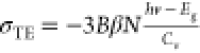 where N, Eg, hv, and Cv are, respectively, the
initial carrier density, bandgap, pump photon energy, and volumetric
heat capacity; (b) DP stress σDP1 = −Nde – (N – n)dh, where n is the filled hole trap density; and (c) local DP stress
where N, Eg, hv, and Cv are, respectively, the
initial carrier density, bandgap, pump photon energy, and volumetric
heat capacity; (b) DP stress σDP1 = −Nde – (N – n)dh, where n is the filled hole trap density; and (c) local DP stress 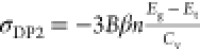 from excess energies of band-edge holes
with respect to the trap energy Et due to hole trapping. The CLAP induced oscillation is superimposed
onto the TR kinetics, which leads to an oscillation frequency of 12
GHz at a probe of 850 nm (Figure 28a). With the use of f ≈ 2nv/λ (where n and λ are the
refractive index and wavelength, respectively), a sound velocity v of 2200 m s–1 associated with the elastic
constant C11 of 20.4 GPa along the ⟨100⟩
crystallographic direction of the crystal is obtained. Meanwhile,
given that the photoinduced stress amplitude depends on the initial
carrier density and excess energies of photoexcited carriers, the
CLAP-induced TR oscillation amplitude varies for different pump energy
and power (Figure 28b). By comparing the CLAP-induced TR oscillation amplitudes of different
pump energies and assuming a negligible trap density, the estimated
total DP: de + dh = −3.93 eV agrees well with the literature report.469 Nevertheless, the above analysis assumed negligible
effects of carrier and heat diffusions on CLAP generation, as well
as an instant energy transfer from HCs to the lattice which need not
be the case, especially for MAPbI3 in which slow HC cooling
with tens of picosecond cooling time under intense photoexcitation
have been widely reported. On the other hand, the dephasing time of
CLAP depends on the crystal’s quality which affects the trap
density and the associated carrier trapping-induced local DP stress.
The upper limits of electron and hole mobilities due to carrier–acoustic
phonon scattering were estimated as 2800 and 9400 cm2 V–1 s–1, respectively, which are much
higher than reported values. The authors attributed this to the reduction
of carrier scattering from optical phonons and defects due to the
polaron effect.
from excess energies of band-edge holes
with respect to the trap energy Et due to hole trapping. The CLAP induced oscillation is superimposed
onto the TR kinetics, which leads to an oscillation frequency of 12
GHz at a probe of 850 nm (Figure 28a). With the use of f ≈ 2nv/λ (where n and λ are the
refractive index and wavelength, respectively), a sound velocity v of 2200 m s–1 associated with the elastic
constant C11 of 20.4 GPa along the ⟨100⟩
crystallographic direction of the crystal is obtained. Meanwhile,
given that the photoinduced stress amplitude depends on the initial
carrier density and excess energies of photoexcited carriers, the
CLAP-induced TR oscillation amplitude varies for different pump energy
and power (Figure 28b). By comparing the CLAP-induced TR oscillation amplitudes of different
pump energies and assuming a negligible trap density, the estimated
total DP: de + dh = −3.93 eV agrees well with the literature report.469 Nevertheless, the above analysis assumed negligible
effects of carrier and heat diffusions on CLAP generation, as well
as an instant energy transfer from HCs to the lattice which need not
be the case, especially for MAPbI3 in which slow HC cooling
with tens of picosecond cooling time under intense photoexcitation
have been widely reported. On the other hand, the dephasing time of
CLAP depends on the crystal’s quality which affects the trap
density and the associated carrier trapping-induced local DP stress.
The upper limits of electron and hole mobilities due to carrier–acoustic
phonon scattering were estimated as 2800 and 9400 cm2 V–1 s–1, respectively, which are much
higher than reported values. The authors attributed this to the reduction
of carrier scattering from optical phonons and defects due to the
polaron effect.
Figure 28.

(a) TR kinetics of MAPbI3 SCs with pump at 550 nm and probe at 850 nm. Inset: Fourier transform of the TR residual after removing carrier recombination and diffusion background. (b) TR oscillation kinetics probed at 850 nm for pump at 550 and 650 nm. (a,b) Reproduced with permission from ref (34). Copyright 2017 Nature Publishing Group. (c) Frequency-domain of CLAPs-induced beating map of MAPbBr3 SCs. (d) Estimated sound velocity for MAPbX3 with different halide ions. (e) Temperature-dependent CLAP oscillation frequency probed at 895 nm. (f) Temperature-dependent TR kinetics of MAPbBr3 across the phase transition. (c–f) Reproduced from ref (470). Copyright 2017 American Chemical Society. (g) CLAPs-induced time-domain beating map after removal of the electronic background of Cs2AgBiBr6 SCs pumped at 400 nm. (h) Normalized TR kinetics of Cs2AgBiBr6 SCs probed at 740 nm showing the CLAPs-induced beating map by different pump energies. (i) Normalized CLAP induced oscillation amplitude as a function of excess energies of photoexcited carriers. The solid line is a linear fit. Reproduced with permission from ref (302). Copyright 2021 American Association for the Advancement of Science.
In another CLAP study on 3D perovskite SCs by Guo et al. using TR spectroscopy, they revealed that both fully inorganic and hybrid perovskite SCs exhibit distinct phonon softening and hardening behaviors with the decrease of temperature across the phase transition from the cubic phase to the orthorhombic phase.470 With above-bandgap photoexcitation, CLAPs were generated through TE stress and DP interaction, as mentioned above. Figure 28c shows a typical frequency-domain CLAPs-induced beating map of MAPbBr3 SCs which displays a decrease of oscillation frequency with increasing probe wavelength in the below bandgap region, as described by f = 2vn/λ. Meanwhile, they found an increase in the sound velocity in MAPbX3 (X = Cl, Br, and I) when the anion radius decreased from I to Br and to Cl (Figure 28d), which was attributed to an increase in bond strength between the Pb and anions. On the other hand, among all the investigated perovskite SCs, besides the phonon hardening in the low-temperature orthorhombic phase, phonon softening is also present in the cubic phase close to the cubic-to-tetragonal phase transition temperature (Figure 28e). The phonon hardening feature can be well explained by the lattice anharmonicity due to the lattice contraction and enhanced bonding strength, whereas the abnormal lattice anharmonicity of phonon softening can be accounted for by the dynamic disorders arising from local polar fluctuations in the cubic phase because of head-to-head motions of the A-site cation along [100] directions.328,471 Meanwhile, this pretransitional phonon softening was found to depend on the relative size of the A-site cation to that of the Pb-X octahedron, with phonon softening CsPbBr3 > MAPbBr3 > FAPbBr3 and MAPbI3 > MAPbBr3 > MAPbCl3. This was attributed to the size-dependent pretransitional structural fluctuations which are stronger when the A cation is smaller, or when the halide ion is larger. Furthermore, the enhanced polar fluctuations which provide additional relaxation pathways for acoustic waves around cubic-to-tetragonal phase transition temperature were also found to result in enhanced oscillation damping (Figure 28f).
Apart from the direct bandgap
HPs, CLAPs are also present in the
indirect bandgap bismuth double perovskites Cs2AgBiBr6 SCs as reported by our group using transient reflectivity
(TR) spectroscopy.302 Congruent with previous
reports, for above-bandgap photoexcitation, the CLAPs were launched
by photoinduced TE stress and DP interaction, leading to a beating
map of tens of GHz in the TR spectrum (Figure 28g). Meanwhile, CLAPs-induced oscillation
is present over nanosecond time scales irrespective of different above-bandgap
pump energies (Figure 28h), and the normalized oscillation amplitude with respect to initial
carrier density increases with excess energies of photoexcited carriers
(Figure 28h), which
is expected given that oscillation amplitude scales linearly with
photoinduced stress σ = 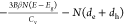 . The estimated total DP of 21.2 eV is consistent
with the DFT calculations of 28.1 eV. Note that our simple analysis
assumed an instantaneous energy transfer from HCs to the lattice and
negligible effects from carrier and heat diffusions. This giant DP
is much larger than that in most of inorganic semiconductors, including
CsPbBr3 with DP of 8.5 eV, and is believed to induce a
strong self-trapping of charge carriers, resulting in a significantly
reduced carrier mobility compared to that of 3D perovskites.
. The estimated total DP of 21.2 eV is consistent
with the DFT calculations of 28.1 eV. Note that our simple analysis
assumed an instantaneous energy transfer from HCs to the lattice and
negligible effects from carrier and heat diffusions. This giant DP
is much larger than that in most of inorganic semiconductors, including
CsPbBr3 with DP of 8.5 eV, and is believed to induce a
strong self-trapping of charge carriers, resulting in a significantly
reduced carrier mobility compared to that of 3D perovskites.
6.2.2.4. Coherent Longitudinal Acoustic Phonon Dynamics in 2D Halide Perovskites
As discussed in section 2, the unique crystal and electronic structures have endowed layered 2D RP perovskites with exceptional optical and electronic properties favorable for photovoltaics and LED applications.46,133,313,474 Nevertheless, their alternating organic–inorganic layered structure has a pronounced influence on the lattice vibrations. The much softer organic spacer layer compared to the rigid inorganic Pb-X (X = I, Br) layer results in a reduced out-of-plane (along the direction perpendicular to the inorganic layer) lattice stiffness compared to the in-plane stiffness. This reduced stiffness leads to a slower CLAP velocity and much weaker thermal conductivity of 2D perovskites compared to their 3D counterparts.409,475
Cross-plane CLAP properties of RP perovskites were first reported by Guo et al. using TR spectroscopy with pump excitation along the out-of-plane direction of the SC flakes.472 The above-bandgap photoexcitation permits CLAPs’ generation via the TE effect and DP interaction. As expected, CLAPs induce a beating map especially at the below-bandgap region of the TR spectrum, as shown in a representative TR spectrum for RP perovskite (BA)2(MA)N−1PbNI3N+1 SCs with N = 1 (Figure 29a). After extracting the real part of the refractive index, the CLAP’s group velocities in RP perovskites with different N were obtained using v = λ/2nT. Compared to 3D perovskite MAPbI3 with v of 2990 m s–1, CLAPs’ group velocities of 2D RP perovskites are smaller (Figure 29b) and increase with the growth of N (N > 1). This was attributed to the smaller acoustic impedance (ρv, where ρ is the mass density) of the organic cation compared to the inorganic PbI6 octahedron. To quantify this reduced CLAPs’ group velocity with a reduction of N, a simple linear coarse-grained bead–spring model was introduced, as shown in (Figure 29c) for N = 2. In this case, the lattice motion dynamics can be described by the following differential equations:
| 53 |
| 54 |
where ma is the
atomic mass and ka and kb are spring constants. Assuming a solution in the form
of u2n+i = U2n+i exp[inl2q – iωt] with q and ω the phonon
wave vector and frequency and l2 = x1 + x2 the lattice
parameter. A similar bead-spring mode was developed for other RP perovskites
with different N. The phonon dispersion matrix can
then be obtained associated with the CLAPs’ group velocity
expressed as  at q = 0. The authors
found that a ka of 17 N m–1 and kb of 1.13 N m–1 can well reproduce the experimental results (Figure 29b) and the CLAPs’ velocity is limited
by kb. Further analysis of the bead-spring
model on out-of-plane CLAPs’ velocity differences between van
der Waals-bonded RP perovskite (BA)2PbI4 and
non-van der Waals-bonded DJ perovskite HAPbI4 shows a significantly
reduced CLAP velocity of the former. This is due to the presence of
the much weaker van der Waals bond between BA cations. Furthermore,
compared to MAPbI3, CLAPs-induced TR oscillation in RP
perovskites damped much faster (Figure 29c,d) due to the presence of CLAP’s
additional scattering pathways, which may stem from the dynamic disorder
and large structural fluctuations of the organic spacer at the aliphatic
ends as well as the strong anharmonicity at the organic–inorganic
interfaces.476,477 Nevertheless, a contrasting
trend of decreasing CLAPs’ group velocity with the growth of N was reported in 2D RP perovskites (PEA)2(MA)N−1PbNI3N+1 (N = 1–3) SCs
by Maity et al. using TR spectroscopy.478 These two distinct results indicate that the
interaction between organic cations plays a significant role in CLAP’s
group velocity of 2D RP perovskites. Further study is warranted to
understand this cation dependence of CLAP’s group velocity
with different N.
at q = 0. The authors
found that a ka of 17 N m–1 and kb of 1.13 N m–1 can well reproduce the experimental results (Figure 29b) and the CLAPs’ velocity is limited
by kb. Further analysis of the bead-spring
model on out-of-plane CLAPs’ velocity differences between van
der Waals-bonded RP perovskite (BA)2PbI4 and
non-van der Waals-bonded DJ perovskite HAPbI4 shows a significantly
reduced CLAP velocity of the former. This is due to the presence of
the much weaker van der Waals bond between BA cations. Furthermore,
compared to MAPbI3, CLAPs-induced TR oscillation in RP
perovskites damped much faster (Figure 29c,d) due to the presence of CLAP’s
additional scattering pathways, which may stem from the dynamic disorder
and large structural fluctuations of the organic spacer at the aliphatic
ends as well as the strong anharmonicity at the organic–inorganic
interfaces.476,477 Nevertheless, a contrasting
trend of decreasing CLAPs’ group velocity with the growth of N was reported in 2D RP perovskites (PEA)2(MA)N−1PbNI3N+1 (N = 1–3) SCs
by Maity et al. using TR spectroscopy.478 These two distinct results indicate that the
interaction between organic cations plays a significant role in CLAP’s
group velocity of 2D RP perovskites. Further study is warranted to
understand this cation dependence of CLAP’s group velocity
with different N.
Figure 29.

(a) Typical below bandgap TR spectrum of 2D RP perovskite (BA)2(MA)N−1PbNI3N+1 SCs for N = 1. (b) Black line with symbol: experimentally measured CLAP group velocities for different N. Green line with symbol: calculated CLAP group velocities using a linear bead–spring model. (c) Schematic of the coarse-grained bead–spring model for N = 2. (d) TR kinetics of RP perovskites with different N and MAPbI3 SCs probed at 955 nm. (e) Fitted coherence time from (d) of the CLAPs-induced TR oscillations for RP perovskites with different N, HAPbI4, and MAPbI3 SCs. (a–e) Reproduced with permission from from ref (472). Copyright 2018 Nature Publishing Group. (f) CLAPs-induced time-domain beating map of the TR spectrum after subtracting the electronic background. (g) Normalized CLAPs-induced TR oscillation amplitude as a function of excess energies of photoexcited carriers for two probes at 542 and 570 nm. (h) Estimated CLAP’s group velocities for RP perovskites (BA)2PbI4 and (PEA)2PbI4 and DJ perovskites (BdA)PbI4 and (4AMP)PbI4. (i) Simulated CLAPs-induced TR oscillation kinetics for different HC cooling time with a probe at 542 nm. (f–i) Reproduced with permission from ref (473). Copyright 2022 American Association for the Advancement of Science.
While basic properties of CLAPs in 2D HPs have
been revealed, a
clear understanding of CLAP’s generation and detection processes
is still lacking. Moreover, it remains unclear how slow HC cooling,
lattice heating, carrier, and heat diffusions affect CLAP’s
generation and detection processes in perovskites. To answer these
questions, we investigated the fundamentals of CLAP’s generation
and detection processes in the archetypal 2D HP (PEA)2PbI4 SCs using TR spectroscopy.473 Congruent
with previous results, we found that CLAPs induced a beating map on
the TR spectrum, which became obvious after subtracting the electronic
background (Figure 29f). Meanwhile, both above- and below-bandgap regions showed CLAPs-induced
oscillations with the former damped much faster than the latter. This
is because the former is dominated by the strong probe light absorption
in addition to the scattering from defects, phonons, and gain boundaries
that govern the latter. On the other hand, we found that CLAPs-induced
oscillation amplitude scales linearly with pump fluence, which is
expected given that the stress-induced TR oscillation amplitude  ∝ σ = σTE + σDP =
  , where d = de + dh. Moreover, by fitting
the pump energy-dependent normalized oscillation amplitude (Figure 29g), the obtained
out-of-plane DP constant d of −4.3 eV agrees
well with our calculated constant of −3.87 eV using DFT calculations.
This negative DP resulted in a reduction of normalized oscillation
amplitude with increasing excess energies of photoexcited carriers.
Furthermore, with DFT calculations, we found that the DP of the VBM
(dh = −2.60 eV) is twice that of
the CBM (de = −1.29 eV), suggesting
that the VBM is more susceptible to the volume deformation potential
than the CBM. This can be attributed to their distinct antibonding
characters in which the VBM mainly consist of Pb 6s and I 5p orbitals,
whereas the CBM is dominated by empty Pb 6p orbitals with negligible
contributions from other orbitals. After the Fourier transform of
the time-domain beating map, we obtained the frequency-domain beating
map. From linear fitting the oscillation frequency ω as a function
of probe light wave vector
, where d = de + dh. Moreover, by fitting
the pump energy-dependent normalized oscillation amplitude (Figure 29g), the obtained
out-of-plane DP constant d of −4.3 eV agrees
well with our calculated constant of −3.87 eV using DFT calculations.
This negative DP resulted in a reduction of normalized oscillation
amplitude with increasing excess energies of photoexcited carriers.
Furthermore, with DFT calculations, we found that the DP of the VBM
(dh = −2.60 eV) is twice that of
the CBM (de = −1.29 eV), suggesting
that the VBM is more susceptible to the volume deformation potential
than the CBM. This can be attributed to their distinct antibonding
characters in which the VBM mainly consist of Pb 6s and I 5p orbitals,
whereas the CBM is dominated by empty Pb 6p orbitals with negligible
contributions from other orbitals. After the Fourier transform of
the time-domain beating map, we obtained the frequency-domain beating
map. From linear fitting the oscillation frequency ω as a function
of probe light wave vector 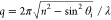 , we estimated the speed of sound (i.e., CLAP group velocity) as 2300 ± 100 m/s, which
agrees well with a previous report.478 On
the other hand, we found that compared to DJ perovskites, the sound
velocities of RP perovskites are smaller due to the weak van der Waals
interactions between organic spacers (Figure 29h). The above-bandgap photoexcitation-induced
acoustic strain modulation to TR spectrum (i.e.,
beating map) was further verified via a two-temperature model consisting
of HC temperature Tc and lattice temperature TL, together with the 1D elastic wave equation
(eq 46), which gives
rise to
, we estimated the speed of sound (i.e., CLAP group velocity) as 2300 ± 100 m/s, which
agrees well with a previous report.478 On
the other hand, we found that compared to DJ perovskites, the sound
velocities of RP perovskites are smaller due to the weak van der Waals
interactions between organic spacers (Figure 29h). The above-bandgap photoexcitation-induced
acoustic strain modulation to TR spectrum (i.e.,
beating map) was further verified via a two-temperature model consisting
of HC temperature Tc and lattice temperature TL, together with the 1D elastic wave equation
(eq 46), which gives
rise to
| 55 |
| 56 |
| 57 |
where N is the exciton density,
τc is the HC cooling time, k1 and k2 are the exciton monomolecular
and Auger recombination coefficients, respectively, D is the exciton diffusion coefficient, CV is the volumetric heat capacity, and k is the thermal
diffusion coefficient. Eq 57 describes the 1D exciton diffusion. With an estimated HC
cooling time of 0.13 ps that barely depends on pump fluence due to
strong Fröhlich interaction arising from the reduced Coulomb
screening effect because of low dielectric permittivity of organic
spacers,242 we simulated the CLAPs-induced
beating map, which matches well with the experimental results for
both above- and below-bandgap regions. Note that in the above two-temperature
model, we assumed a negligible effect from the fast phonon scattering
process in 2D HPs. Meanwhile, we found that heat and carrier diffusions
play negligible roles in CLAPs’ generation and the resultant
oscillation amplitude, which is due to the smaller-than-unity values
of  and
and  (where α is the absorption coefficient),
respectively.479 On the other hand, our
proposed two-temperature model shows that slow HC cooling reduced
the oscillation amplitude because of a more uniform distribution of
lattice temperature (Figure 29i). Note that instead of using the three-temperature model458 which consists of HCs, LO phonons, and the
lattice, we employed a simple two-temperature model and neglected
the fast LO phonon scattering process (τLO < 1
ps) in 2D halide perovskites which has minimal effect on CLAPs’
generation and the resultant ΔR/R modulation. This summarizes the current state of CLAP dynamics studies
in 2D perovskites.
(where α is the absorption coefficient),
respectively.479 On the other hand, our
proposed two-temperature model shows that slow HC cooling reduced
the oscillation amplitude because of a more uniform distribution of
lattice temperature (Figure 29i). Note that instead of using the three-temperature model458 which consists of HCs, LO phonons, and the
lattice, we employed a simple two-temperature model and neglected
the fast LO phonon scattering process (τLO < 1
ps) in 2D halide perovskites which has minimal effect on CLAPs’
generation and the resultant ΔR/R modulation. This summarizes the current state of CLAP dynamics studies
in 2D perovskites.
7. Carrier Diffusion, Funneling, Extraction, Recombination, and Photon Recycling
In this section, our attention turns to the later processes from picosecond to the microsecond time scale and beyond on the “removal” of the photoexcited species from the excited region. The features that propel HPs as frontrunners in various optoelectronics applications are their outstanding intrinsic charge and transport properties. These properties are relevant to the performance of HPs as an active layer in a device, either as a light absorber or an emitter. They include charge carrier diffusion in the perovskite layer, extraction from the perovskite, transfer mechanisms including funneling and charge carrier recombination as well photon recycling, which will be reviewed in the following sections.
7.1. Carrier Diffusion
The outstanding performance of solution-processed HP absorber layer in a broad range of solar cell configurations first stoked interest in HP’s charge diffusion properties.1,2,480 The 2013 seminal works by Xing et al.(89) and Stranks et al.(6) validate that both electrons and holes in the archetypal MAPbI3 system possess diffusion lengths on the order of hundreds of nanometers. This was accomplished by performing TRPL and TA spectroscopy studies. The PL from free electrons and holes was quenched due to their extraction when interfaced with the electron and hole transporting materials typically used in solar cells. To quantify the carrier diffusion in a film, the carrier diffusion is usually modeled using a simple 1D differential equation given as
| 58 |
where D is the diffusion
constant along the z-axis, N(z,t) is the carrier density, and k is the
carrier recombination rate. Numerical solutions to this equation can
be obtained by assuming an initially exponential carrier distribution
created quasi-instantaneously by the pulsed laser excitation. In the
estimation, complete quenching by the electron and hole transporting
layers is usually assumed, thus giving a lower limit of the carrier
diffusion coefficient. The diffusion length LD can then be calculated as  , where τ = 1/k is
the PL lifetime. The electron and hole diffusion lengths are in general
limited by grain boundaries and defects that are inevitably present
in the solution-processed HPs. With the synthesis of high-quality
HP SCs, these extrinsic factors can be excluded, and thus the intrinsic
carrier diffusion properties can be distilled. The diffusion lengths
of 3D HP SCs are more than several micrometers, reinforcing their
exceptional transport properties.7,481,482 The large carrier diffusion lengths of HP SCs are
attributed to the small effective masses of the electron and hole96,108,483,484 that enhances charge mobility and the long recombination lifetime
aided by its good defect tolerance. This will be discussed in detail
later.
, where τ = 1/k is
the PL lifetime. The electron and hole diffusion lengths are in general
limited by grain boundaries and defects that are inevitably present
in the solution-processed HPs. With the synthesis of high-quality
HP SCs, these extrinsic factors can be excluded, and thus the intrinsic
carrier diffusion properties can be distilled. The diffusion lengths
of 3D HP SCs are more than several micrometers, reinforcing their
exceptional transport properties.7,481,482 The large carrier diffusion lengths of HP SCs are
attributed to the small effective masses of the electron and hole96,108,483,484 that enhances charge mobility and the long recombination lifetime
aided by its good defect tolerance. This will be discussed in detail
later.
The charge transport efficiency in HPs is usually assessed based on the charge carrier mobility μ, which is related to the diffusion coefficient D via the Einstein–Smoluchowski relation:
| 59 |
where e is the electronic charge. This carrier mobility can be directly measured using various nonspectroscopic techniques such as space-charge limited conduction (SCLC),7,485,486 Hall effect measurement,487,488 time-resolved microwave photoconductivity,489−491 and time-of-flight measurements,7,481,492 as well as contact-free spectroscopic techniques such as the PL quenching method.6,89 For the former, the measurement could be compromised by the ion migration effect in HPs under electric field493 and may be affected by the device contacts, whereas the latter is valid under specific assumptions. Next, we briefly distill the reported results from various contract-free spectroscopic techniques as well as their limitations.
One of the commonly used contract-free technique is the PL quenching spectroscopy, which allows the determination of the electron and hole mobility separately with the aid of the diffusion model.6,89 Nevertheless, this method is valid only under the assumption that all the charge carriers are extracted to the extraction layer. Therefore, the estimated diffusion lengths and carrier mobilities by this method represent the lower limits of their intrinsic properties. As shown in Table 2, the diffusion lengths of polycrystalline 3D HPs measured using this PL quenching technique are in the range of hundreds of nanometers.
Table 2. Reported Carrier Mobilities and Diffusion Lengths of HPs Measured Using Various Spectroscopic Techniques (At Room Temperature)a.
| material | technique | diffusion length LD (μm) | carrier mobility μ (cm2 V–1 s–1) | diffusion coefficient D (cm2 s–1) | ref |
|---|---|---|---|---|---|
| polycrystals | |||||
| MAPbI3 | PL quenching | < 0.13 (e), < 0.09 (h) | 1.40 (e), 0.86 (h) | 0.036 (e), 0.022 (h) | (89) |
| MAPbI3 | PL quenching | < 0.129 (e), < 0.105 (h) | 0.66 (e), 0.43 (h) | 0.017 (e), 0.011 (h) | (6) |
| MAPbI3-xClx | PL quenching | < 1.069 (e), < 1.213 (h) | 1.63 (e), 2.10 (h) | 0.042 (e), 0.054 (h) | (6) |
| MAPbI3 | THz conductivity | ∼2.5 | ∼30 | ∼0.78 | (497) |
| MAPbI3-xClx | THz conductivity | ∼2 | ∼11.6 | ∼0.30 | (496) |
| FAPbI3 | THz conductivity | ∼25 | ∼75 | ∼1.93 | (494) |
| MAPbI3 | transient absorption microscopy | ∼1.2 | 1.4–3.11 | 0.05–0.08 | (504) |
| MAPbI3 | transient grating | ∼1.9–3.8 | 19.5–77.82 | 0.5–2.0 | (510) |
| MAPbI3 | transient grating | ∼0.95 | ∼66.15 | ∼1.7 | (509) |
| (PEA)2PbI4 | PL microscopy | 0.24 | ∼7.47 | 0.192 (x) | (506) |
| BA)2(MA)n−1PbnI3n+1 | transient absorption microscopy | 0.16 (n = 1) – 0.67 (n = 5) (x) | 2.33 (n = 1) – 13.23 (n = 5) (x) | 0.06 (n = 1) – 0.34 (n = 5) (x) | (507) |
| single crystals | |||||
| BA)2(MA)n−1PbnI3n+1 | scanning photocurrent microscopy | 7 (n = 1) – 14 (n = 3) | – | – | (402) |
| MAPbI3 | scanning photocurrent microscopy | 18 | – | – | (402) |
| MAPbI3 | SCLC and transient PL | 2–8 | 2.5 | ∼0.06 | (7) |
| MAPbBr3 | Hall effect and transient PL | 3–11 | 20–60 | ∼0.51–1.54 | (7) |
| MAPbBr3 | transient PL | 2.8–4.4 | 310–820 | 8–21 | (499) |
| MAPbI3 | transient PL | – | >50 | >1.28 | (501) |
| MAPbI3 | THz conductivity | – | 500–800 | ∼12.8–20.6 | (115) |
| FAPbBr3 | transient reflectance | – | 28.4 | 0.73 | (502) |
| nanocrystals | |||||
| MAPbBr3 | PL microscopy | 0.8–1.1 | 5.9–10 (x) | 0.15–0.27 (x) | (505) |
| CsPbBr3 | transient PL microscopy | ∼0.2 | 19.45 | 0.5 (x) | (508) |
| CsPbBr3 | TA | 0.24 | 2.1 (e), 0.69 (h) | 0.05 (e), 0.02 (h) | (503) |
Diffusion coefficient D and mobility μ are related by the Einstein-Smoluchowski Relation. This relation is used to calculate the italicized values in this table, in cases when either value is not reported in the literature. Here, e, h, and x refer to the electron, hole, and exciton, respectively. If the type of carrier is not specified, the reported value indicates the total mobility of all the carriers.
In comparison, the THz conductivity technique allows direct probe of the charge carrier mobility via measuring the photoconductivity of the sample.115,391,494−498 This technique usually requires fitting the photoconductivity spectrum with specific models, with the Drude model being used extensively for HPs. Furthermore, the measurements may be affected by different substrates used. These two factors may explain the large variation in the values reported by different research groups. On the other hand, the reported carrier mobilities of HP SCs measured using this THz technique are much larger than those measured using complementary techniques.115 To rationalize these differences, it is therefore necessary to conduct comparison measurements with other spectroscopy techniques and analyze their respective limitations.
Another useful technique is the two-photon excitation spectroscopy with a below-bandgap pump that affords a deeper penetration depth. This is especially effective for measuring charge carrier diffusion of thick samples like SCs compared to using conventional one-photon excitation.499−501 Other than the aforementioned approaches, TA and TR spectroscopies have also been employed to track the carrier propagation in the sample.502,503 Additionally, the use of microscopy131,284,504−508 and transient grating509,510 techniques help further visualize the in-plane carrier diffusion.
Table 2 summarizes the reported carrier diffusion lengths and mobilities of HPs with different compositions and dimensionalities using different techniques. As shown in Table 2, the reported carrier diffusion properties of HPs are strongly dependent on the sample’s morphology and dimensionality as well as the technique used.511,512 Carrier diffusion lengths of several micrometers were reported in 3D HPs polycrystalline films compared to less than 1 μm in 2D HPs. Perovskite SC possesses longer diffusion lengths (up to tens of micrometers) and higher mobilities compared to polycrystalline films. For perovskite NCs, diffusion proceeds via exciton hopping or energy transfer. Their carrier diffusion length is expected to be lower as their carrier diffusion dominated by exciton hopping or energy transfer will be limited by the insulating ligand molecules. Nevertheless, carrier diffusion lengths longer than 1 μm were reported by Giovanni et al. in spin-coated perovskite NC films which were attributed to photon reabsorption and remission (i.e., photon recycling effect).505 This photon recycling effect in HPs will be reviewed in detail in section 7.5
Carriers in HPs are more mobile compared to molecular systems, whose reported diffusion lengths are in the range of tens of nanometers.497 For conventional inorganic semiconductors such as Si and GaAs513−515 whose mobilities are in the range of thousands of cm2 V–1 s–1, carrier mobilities of HPs are still considerably lower (Table 2). Considering that carrier effective masses of HPs are comparable to those of conventional inorganic semiconductors, the intrinsic carrier mobility of HPs will be limited by the carrier-phonon interactions. Furthermore, the carrier mobility of HPs can also be reduced by the presence of structural disorder, as observed in mixed composition HPs516 and quasi-2D perovskites,517 which possess more complex crystalline structures and orientations that are affected by the organic spacers. Notably, for HP’s device applications where charge transport is crucial, their defect tolerance and long charge carrier lifetimes help to offset the effect of lower mobility and assists in charge extraction. For a comprehensive discussion on electron and hole mobilities of HPs, the interested reader is referred to the recent excellent reviews.518−520
7.2. Carrier Funneling
The chemical compositions and dimensionality (from 0D to 3D) of HPs are highly tunable,521 such as through mixed-halide,516,522 mixed-A-site cation,523−525 mixed-dimensionality,51,98 as well as large organic cations incorporation526−532 in quasi-2D HPs. Mixed composition, alloying, or large organic cation incorporation infuses HPs with structural disorder and a complex energy landscape distinct from conventionally ordered 3D perovskite crystalline lattice. Mixed-halide or mixed-dimensionality phases within HPs transform the local energetics that can cause the transfer of photoexcited charge carriers from the high-energy regions (i.e., larger-bandgap phases) to the low-energy regions (i.e., lower-bandgap phases). Such transfer also known as funneling plays a crucial role in the early time carrier dynamics. For instance, in mixed-halide perovskites like MAPbIzBr3–z, localized domains rich in iodide with smaller bandgap will coexist with those rich in bromide with a larger bandgap to maintain the stoichiometry. Charge carriers in the latter will migrate to the former due to the energetic gradient, increasing the carrier population in the former where they eventually recombine and give a red-shifted emission. It is challenging to precisely control this process in mixed-halide perovskites for PeLEDs where halide segregation has an adverse impact on the color purity.69,533,534 In the following subsections, we focus mainly on quasi-2D HPs.
7.2.1. Funneling in Quasi-2D Halide Perovskites
Low-dimensional HPs generally possess lower carrier mobility and shorter carrier lifetime compared to 3D HPs due to the carrier confinement effects. Hence, funneling could help improve carrier transport in mixed-dimensionality HPs. In fact, carrier funneling has been widely reported in the quasi-2D RP perovskites (L2An–1BnX3n+1), which form alternating organic–inorganic multiple quantum well (MQW) structures that possess a type-I band alignment, as the organic layer has a larger bandgap than the inorganic layer.535−537 As mentioned in section 2.2, with increasing n (i.e., the number of the inorganic octahedra layer), the reduction of electronic confinement along the direction perpendicular to the 2D layer leads to a decrease in their bandgaps. At the upper limit of very large n, the bandgap and the electronic structure of quasi-2D HPs approach that of bulk 3D HPs.98 Nevertheless, it is challenging to obtain pure phase quasi-2D RP perovskite films using solution-processing. Usually one obtains a distribution of QWs with different thicknesses and bandgaps that are interspersed by the organic spacer molecule forming the barrier.
Yuan et al. reported the first work on charge carrier funneling in these quasi-2D RP perovskite systems.538 They found that the lower-bandgap phases of quasi-2D RP perovskite with higher n can act as charge carrier concentrators (Figure 30a), as evident from the TA spectra (Figure 30b). They proposed that funneling could enhance radiative recombination in the localized domains while outcompeting trapping and other nonradiative recombination channels.539 The luminescence efficiency of these materials is thus enhanced since the radiative recombination rate in the exciton-dominated 2D phases is larger at low carrier densities. Typical funneling time constants are between 0.1–100 ps.
Figure 30.

Charge carrier funneling in RP perovskites. (a) Schematic representation of charge carrier migration from low-⟨n⟩ phase to high-⟨n⟩ phase in a mixed-phase RP perovskite film. The different colors represents QWs with different thickness ⟨n⟩. Reproduced with permission from ref (538). Copyright 2016 Nature Publishing Group. (b) TA spectra of (PEA)2(MA)n−1PbnBr3n+1 films at different probe delay times. The PB signal from the higher-energy phases decreases while that from the lower-energy phases increases because of exciton transfer/funneling. Reproduced with permission from ref (539). Copyright 2017 American Chemical Society. (c) Energy level alignment at the interface of n = 1 and n = 3 RP phases modulated by the organic ligand density. (Right) (i) PEAI ligand-rich interface has a type-I alignment while (ii) PEAI-depleted interface has a type-II alignment, as shown in the calculated bands on the left. The authors note that only the VBM are accurate in the calculated result. Reproduced with permission from ref (540). Copyright 2019 American Chemical Society. (d) PB kinetics corresponding to different n-phases of (NMA)2(FA)n−1PbnI3n+1. Green and black curves corresponding to lower-n phases get quenched fast while the higher-n phases (red) curve exhibits simultaneous growth. Dynamics involve both fast and slow rise times attributed to two different processes. Reproduced with permission from ref (401). Copyright 2017 Nature Publishing Group. (e) 2DES spectrum of (PEA)2(MA)n−1PbnI3n+1 at a waiting time of 10 fs. Horizontal and vertical lines correspond to the resonance energies of n = 2 to 5 phases. Marked circles indicate the cross-peaks indicating ultrafast transfer of carriers among these phases. Reproduced from ref (541). Copyright 2019 American Chemical Society.
7.2.1.1. Energy v.s. Charge Transfer
Although the funneling phenomenon in quasi-2D HPs is widely reported, a clear understanding of the underlying mechanisms remains fragmented. Here, we focus on the funneling mechanisms in the archetypal RP perovskite. While several studies indicate that the funneling involves the exciton transfer from low-n to high-n RP phases (or equivalent QWs),132,401,527,538,540,542,543 others attribute this process to the transfer of electrons and holes.529,544−547 To clarify these competing claims, it is imperative to first establish the interfacial band alignment between different phases. While a type-I energy-level alignment facilitates energy transfer from the high-energy domain toward the low-energy domain, a type-II energy-level alignment facilitates charge carrier separation and transfer. Nevertheless, precise determination of the energy level alignments can be challenging due to the complex spatial distribution of different phases, low phase purity, as well as the influence of organic cations on the chemical environment. For instance, Quintero-Bermudez et al. found that the local energy-level alignment among different phases is affected by the density of organic molecules at the interfaces, and the band alignments are shifted after surface treatment.540 As evident from Figure 30c, a ligand-rich interface results in the formation of a type-I alignment whereas a ligand-depleted interface leads to a type-II interface. This could explain the different types of band alignment reported in the literature, and it implies that the phase composition could be engineered to facilitate charge concentration (type-I) or charge separation (type-II).
Apart from interfacial energy-level alignment, the interaction between charge carriers localized in different QWs also have a role in the funneling process. This interaction is mainly dictated by two factors: the inter-QW separation and the electronic coupling between the initial and final QW states, which determine whether the funneling is through an energy transfer or a charge transfer process. Inter-QW energy transfer proceeds via dipole–dipole coupling described by the Förster resonance energy transfer model, which gives rise to the following energy transfer rate:548,549
| 60 |
where VDA is the electronic coupling between the donor and acceptor QW, J is the overlap integral of the donor emission spectrum and acceptor absorption spectrum, and d is the separation between adjacent QWs mainly determined by the length of the organic cation spacer. Conversely, the charge transfer between different QWs is described by the Marcus theory, which gives rise to the following charge transfer transfer rate:550,551
| 61 |
where k0 is a constant that is proportional to the square of the transition matrix element between the donor and acceptor states and β is an attenuation constant that depends on the barrier material between different QWs. As evident from eqs 60 and 61, these two processes exhibit different distance dependences, which is however difficult to differentiate based on a simple spectroscopy measurement. Distinguishing which process dominates the early time carrier dynamics in these quasi-2D HPs necessitates careful investigation of the ultrafast carrier dynamics using advanced spectroscopies.
Our group investigated the exciton funneling in the mixed-dimensional RP perovskite (NMA)2FAn–1PbnI3n+1 (NMA = naphthyl-methylammonium) films using TA spectroscopy in one of the earliest reports.401 The funneling signature is evident from the simultaneous decay of the PB signal of large-bandgap phases (i.e., PB2 and PB3) and the rise of the PB signal of small-bandgap phases (PBn) (Figure 30d). The funneling process comprises a fast process (∼0.5 ps) due to exciton localization to nearby QWs and a slower process (∼200 ps) corresponding to exciton localization to nonadjacent QWs. To distinguish between energy and charge transfer, Zheng et al. performed TRPL and TA measurements on mixed-dimensional RP perovskite films with different inter-QW distances.552 While TA is sensitive to the population of charges as well as excitons, TRPL is less sensitive to the separated charges. Hence, by comparing the early time dynamics from TRPL and TA spectroscopies, they established the evidence of charge transfer from the thinner quantum wells to the thicker ones. They found that shorter spacing cations can significantly enhance both the inter-QW charge and energy transfer and facilitate the exciton transfer from 2D to 3D phases even under high-intensity light excitation, while suppressing the high-order charge recombination process.
With the aid of more advanced spectroscopy techniques like multidimensional spectroscopy, researchers have also successfully decoupled these two transfer processes and clarified the underlying funneling mechanisms. Proppe et al. employed the 2DES technique, which provides simultaneous high-temporal and spectral resolution, to elucidate the inter-QW coupling in mixed perovskite QWs.541 By analyzing the cross-peaks in the 2DES spectrum (Figure 30e), they showed that the energy transfer from high-energy phase to low-energy phase proceeded over a time scale of 0.2–0.3 ps, which matched the results from the inter-QW Förster theory. Meanwhile, they also observed a slow hole transfer over the time scale of 10–100 ps using TA spectra. To clarify the charge transfer dominated funneling process, they performed nonadiabatic molecular dynamics simulation and estimated the free charge transfer rate. Consistent with TA measurements, they found that a weak coupling between free carrier states in different QWs leads to a slow charge transfer rate on the order of several picoseconds. Their results provide a conclusive picture that could well explain previous reports: excitons in RP perovskites transfer from high-energy phases toward low-energy phases at subpicosecond time scale, while the charge transfer of free electrons and holes dominate at longer time scales. Similar results have also been reported by other groups.553,554
7.2.1.2. Role of the Organic Spacer
After clarifying the main funneling mechanisms, it is important to establish the key factors that influence the funneling efficiency in RP perovskites. The funneling efficiency could be limited by structural parameters such as relative QW distribution and orientation which are influenced by the organic spacer. Quintero-Bermudez et al. investigated the formation mechanism of the RP perovskite phases in a film.526 They found that the organic spacer, solution processing steps, and choice of solvents played crucial roles in the QW thickness distribution as well as their orientation in the film, thereby ultimately impacting the funneling dynamics. The additional flexibility in tuning RP perovskites’ energy landscape from the large library of organic spacers and solution-processing routes thus afford exciting opportunities for judcious tailoring of their optoelectronic properties.526−532
As mentioned earlier, inter-QW coupling is strongly influenced by the interlayer spacing that is determined by the organic spacer and the relative layer orientation in the film.540,552 Hence, inter-QW energy transfer can be modulated by regulating the coupling between the donor and acceptor QWs as the chemical composition of quasi-2D perovskite films can be optimized. Note that the Förster energy transfer model is only applicable to weak coupling between the donor and acceptor QWs. When inter-QW coupling is relatively strong and in the presence of weak exciton-bath interactions, a new energy transfer picture for coherent energy transport comes into play.557−559 In this case, the wave function is delocalized over several QWs until it eventually collapses due to decoherence. Recent experimental works have demonstrated that such coherent energy transport-induced wave function delocalization could be realized in quasi-2D HPs. For instance, Elkins et al.(560) observed a delocalized biexciton state between n = 2 and n = 3 phases in (BA)2(MA)n−1PbnI3n+1 QWs using double quantum coherence spectroscopy. Using broadband TA spectroscopy together with theoretical calculations, Zhai et al.(561) found that excitons in (PEA)2PbI4 2D perovskite were delocalized over ∼10 nm, which extends across several QW layers. Sichert et al. performed PL experiments on RP perovskite films with linear alkylammonium organic spacers of different lengths.555 They considered the RP perovskite structure along its stacking axis as a superlattice (Figure 31a) and calculated the electron and hole energies for their different spacer (barrier) lengths. They found that shorter spacers enhanced the electronic coupling across the spacer, resulting in the miniband formation and decrease of the bandgap, consistent with their PL experiments (Figure 31b). Our group showed that such miniband formation is a precursor to coherent energy transfer in RP perovskite films.132 By extending the superlattice model as well as accommodating different spacers and QW widths, we showed that the carrier wave functions could leak through finite barriers defined by the spacer, resulting in the interlayer energy transfer over subpicoseconds time scale. We further simulated the exciton wave function localization in a simple case of a two-QW system (Figure 31c). Furthermore, together with TA spectroscopy, we found an ultrafast carrier transfer from low-energy to high-energy QWs (Figure 31d), which we attributed to a coherent back-transfer.
Figure 31.

Carrier delocalization in quasi-2D HPs. (a) Schematic representation of a QW superlattice and the associated DOS. The miniband formation leads to bandgap tuning of confined phases. (b) Calculated bandgap of the superlattice using a Kronig-Penney model as a function of the width of the barrier organic spacer. (a,b) Reproduced with permission from ref (555). Copyright 2019 AIP Publishing. (c) Simulated probability density for a two-QW (n = 2 and 3) system using a finite-QW superlattice model. Excitation is initially in n = 2 QW. The wave function leaks across the finite barrier potential. (d) Coherent excitation back-transfer of two QWs from n = 3 to n = 1 after directly exciting the n = 3 exciton state. (c,d) Reproduced from ref (132). Copyright 2021 American Chemical Society. (e) 2DES spectrum of (BA)2(MA)n−1PbxI3n+1 film, with horizontal and vertical lines indicating the resonance energies of n = 3 to 6 phases. The broad signal response with strong above and below diagonal signal indicates carrier delocalization from the n = 3 to 6 phases. (f) 2DES spectrum of (PEA)2(MA)n−1PbxI3n+1 with the same n = 3 to 6 phases marked by straight lines. The signal response has very weak cross-peaks, indicating weak inter-QW coupling and absence of delocalization. (e,f) Reproduced with permission from ref (556). Copyright 2022 Wiley-VCH.
Coherent multidimensional spectroscopies including 2DES are powerful tools for characterizing structural and energetic disorders in these systems as well as tracking the coherent energy transfer. This is highlighted in our recent work using 2DES to probe the ultrafast spectral and temporal dynamics in these multiple phase systems.556 We found that a simple change of organic spacer cation alters the RP perovskite energy landscape. 2D maps at different waiting times are generated which provide elaborate information on inter-QW couplings and their time evolution. In our 2DES experiments, we observed a spectrally correlated response with above and below-diagonal cross-peaks for (BA)2(MA)n−1PbnI3n+1, which indicated that carriers are delocalized across n = 3 to n = 6 phases (energy levels denoted by vertical and horizontal lines on the 2D maps in Figure 31e) that promote enhanced transport via coherent transfer. Such delocalization was, however, not observed in (PEA)2(MA)n−1PbnI3n+1, which has a longer spacer (Figure 31f). Together with TA spectroscopy, we proposed that the cascade energy transfer from the lower to higher-n phases in the BA-based film is more efficient. For the PEA-based film, the weaker inter-QW coupling is correlated with a more efficient carrier extraction from the lower-n phases. These results demonstrate that organic spacer cation modulates the energetic disorder in quasi-2D perovskite film.
Nevertheless, studies on such coherent transport dominated inter-QW interactions in quasi-2D systems are still limited.562 Note that coherent exciton transport could be hindered by strong exciton–phonon coupling, which will cause rapid dephasing and impact the quantum dynamics. For instance, Zhang et al. found that strong electron–phonon coupling accelerates the dephasing which becomes faster with increasing n in 2D RP perovskites.563 Meanwhile, a strong exciton–phonon coupling has been found to induce fast solvation-like dynamics (∼100 fs) of the line shape in quantum-confined HP NCs, which could be detrimental to exciton delocalization in the quasi-2D systems.304 Investigation of ultrafast dynamics in systems with stiffer and shorter spacers such as DJ perovskites is warranted to better understand this coherent transport in the quasi-2D systems.473,564
In summary, quasi-2D perovskites present an exciting playground for exploring novel photophysics. By harnessing the funneling effect, it could lead to unconventional applications.136 For instance, we found that exciton funneling is also spin-preserving, which leads to long-range spin funneling in RP perovskite films.565 There is an urgent push for advances in synthesis and characterization methods to exploit the potential of quasi-2D perovskites. Synthesis of phase-pure 2D perovskites133,134 are critical for deterministic fabrication of 2D-perovskite-based heterostructures,566 which will be ideal model systems for studying their fundamental photophysics as well as for optimizing device performance.136
7.3. Carrier Extraction
In section 7.1, we discussed the long carrier diffusion lengths and the long carrier recombination lifetimes of HPs. While their exceptional charge transport properties are a crucial baseline for optoelectronic applications, equally important are the interfacial phenomena following the charge diffusion from the bulk film to the charge separation/extractor layer. This entails (1) fast charge carrier transfer from HP to the extractor before they recombine within the HP, and (2) a well-engineered interface with suitable energetic alignment and devoid of the potential barrier, interfacial dipoles, surface defects, etc. The latter is a particularly challenging area of research that focuses on designing high-quality materials and interfaces to support efficient extraction. The quality of the interface is also intertwined with the eventual efficiency of extraction of charges from the HP. Notwithstanding, this review will focus on the first issue: the properties of HPs for efficient charge extraction in terms of their intrinsic photophysics.
Our group investigated the electron and hole extraction dynamics in the MAPbI3 layer using TA and TRPL spectroscopies in one of the earliest photophysics studies.89 The MAPbI3 film was interfaced with an electron transport layer of Phenyl-C61-butyric acid methyl ester (PCBM) and a hole transport layer of Spiro-OMeTAD. The PL intensity from carrier recombination in MAPbI3 was quenched in the presence of both electron and hole extraction layers (Figure 32a). By comparing the PL decay lifetime of the neat MAPbI3 films (τ0) and MAPbI3 films when interfaced with charge extraction layers (τ1), we obtained the electron and hole extraction time τCT (here, τ1–1 = τ0 + τCT–1) as ∼0.40 and ∼0.75 ns with extraction efficiency (i.e., τ1/τCT) of 92% and 86%, respectively. Similar quenching was also reported by Stranks et al. in chloride-doped and undoped MAPbI3 films.6 Using the same PL quenching experiment, Docampo et al. found that the charge carriers in MAPbI3 could also be efficiently extracted by an array of different electron and hole acceptor materials used in organic photovoltaics.568
Figure 32.

Charge carrier extraction from perovskite. (a) TRPL decay kinetics of MAPbI3 films probed at ∼760 nm on quartz (black) and when interfaced with an electron extraction layer of PCBM (red) and hole extraction layer of Spiro-OMeTAD (blue). Reproduced with permission from ref (209). Copyright 2014 The Royal Society of Chemistry. (b) TA kinetics of MAPbI3 films when interfaced with TiO2 (black) and Al2O3 (blue), and MAPbI3/Spiro-OMeTAD films when interfaced with TiO2 (red) and Al2O3 (green). Films were pumped at 580 nm and probed at 1.4 μm. Relative amplitude of the slower part of the TA decay is compared to rationalize the extraction of electrons and holes by TiO2 and Spiro-OMeTAD, respectively. Reproduced with permission from ref (567). Copyright 2014 Nature Publishing Group.
Kim et al., using TA spectroscopy, provided direct evidence of electron and hole extraction from MAPbI3 films to the electron transport layer of TiO2 and hole transport layer of Spiro-OMeTAD, respectively, based on the ultrafast quenching of the TA signal.1 Later, using the same technique but with a mid-infrared probe that detects photoexcited electron and hole population in the MAPbI3 layer, Marchioro et al. found that when MAPbI3 or MAPbI3/Spiro-OMeTAD was interfaced with TiO2 (electron transport layer), the relative amplitude of the TA signal at the slower decay (at a delay of ∼25 ps) is larger compared to that on Al2O3 where there is no electron injection (Figure 32b).567 They assumed that the charge recombination in MAPbI3 is similar on TiO2 and Al2O3. The stronger TA signal for MAPbI3 interfaced with TiO2 was thus attributed to the ultrafast electron injection, which left an excess of holes in MAPbI3. Meanwhile, they found that the electron and hole injection at the interface proceeded within the first 3 ps after photoexcitation. These ultrafast time scales of interfacial electron and hole transfer are consistent with later studies on charge extraction at the HP-extractor interface using TA spectroscopy.569−572 A complementary study by Ponseca, Jr. et al. using time-resolved terahertz spectroscopy provided further evidence of this ultrafast charge carrier extraction in the MAPbI3/TiO2 system.391
It is important to note that electron and hole extraction efficiency ultimately depends on several material parameters, including HP composition,380 defect density,573 and film thickness570 as well as interfacial energy-level alignment. Furthermore, charge extraction is also affected by the HC cooling, which is relatively slow in HPs, as discussed previously. Nevertheless, HC extraction is advantageous for energy conversion although designing favorable interface energetics remains challenging.292,295,556 The presence of potential barriers at the HP-extractor interfaces is also detrimental for carrier extraction.574−576 Moreover, ion migration, which has been widely reported in HPs during device operations, may also severely impact charge extraction.577 Comprehensive discussions on these topics are detailed in related excellent reviews on these topics.66,493
7.4. Carrier Recombination
Following ultrafast carrier generation and HC cooling, the carriers will relax to their ground state via different orders of the recombination processes. Typically, for free carriers, these processes include first-order nonradiative trap-mediated monomolecular recombination, second-order radiative bimolecular recombination, and third-order Auger recombination. For excitons, they include first-order recombination and second-order Auger recombination. The overall carrier recombination process strongly depends on the film morphology, temperature, exciton binding energy, and carrier density, etc.
After pulsed laser excitation, these different orders of carrier recombination processes can be traced using various time-resolved characterization techniques. For instance, TRPL spectroscopy tracks the emissive carrier recombination while TA spectroscopy detects the total population of photoexcited carrier density. Combined with complementary techniques such as TRTS, time-resolved microwave conductivity, as well as PLQY studies, etc., a clear picture of these recombination processes over a broad range of carrier densities from ∼1013 to ∼1020 cm–3 can be obtained. In general, the free carrier population dynamics can be described by a simple differential equation given by
| 62 |
where G is the carrier generation date and k1, k2, and k3 are the monomolecular, bimolecular, and Auger recombination constants, respectively. Here, k1 refers to the trap-mediated recombination, k2 corresponds to the radiative bimolecular recombination, and k3 is related to the nonradiative Auger process. Note that for population dynamics dominated by excitons, there is no fourth term (k3n3) on the right side of eq 62. Instead, the third term (k2n2) refers to the many-body Auger recombination process. In the following subsections, we will discuss these processes in detail. Considering that the carriers are generated instantaneously under pulsed photoexcitation, we can therefore ignore the carrier generation term in eq 62. The rate constants in eq 62 are usually extracted by global-fitting the power-dependent TRPL or TA kinetics. Figure 33a shows the typical fluence-dependent charge carrier dynamics and the curve fits in MAPbBr3 using TA spectroscopy. Representative rate constants k1, k2, and k3 for several 3D HPs obtained by this global-fitting approach with time-resolved techniques are shown in Table 3. We will also be separately discussing these recombination channels as well as their origins in the following subsections.
Figure 33.

Charge Carrier Recombination in HPs. (a) Rate constants estimation by global-fitting the excitation intensity-dependent TA kinetics in MAPbBr3. Reproduced from ref (578). Copyright 2015 American Chemical Society. (b) Trap density estimation in MAPbI3 polycrystalline film using eq 65. Reproduced with permission from ref (579). Copyright 2014 Nature Publishing Group. (c) Schematic illustrating the interplay of trap-mediated monomolecular and bimolecular recombination processes in MAPbI3 films at low and high pump fluences. Reproduced with permission from ref (580). Copyright 2014 American Physical Society. (d) PL intensity and radiative recombination lifetime as a function of excitation fluence, illustrating the crossover from trap-mediated monomolecular to bimolecular recombination process. Reproduced from ref (581). Copyright 2014 American Chemical Society.
Table 3. Experimentally Determined Rate Constants by Performing Global Fit on Transient Spectroscopy Data Using Eq 62.
| material | k1 | k2 | k3 | method | ref. |
|---|---|---|---|---|---|
| MAPbI3 | 15 × 106 | 0.6 × 10⁻¹⁰ | 1.6 × 10⁻²⁸ | TRTS | (497) |
| MAPbBr3 | 27 × 106 | 4.9 × 10⁻¹⁰ | 13.5 × 10⁻²⁸ | TA | (578) |
| FAPbI3 | 0.9 × 10⁶ | 7.0 × 10⁻¹⁰ | 3.0 × 10⁻²⁸ | TRPL, PLQY | (401) |
| FAPbBr0.55I0.45 | 45 × 106 | 17 × 10–10 | 0.4 × 10⁻²⁸ | TRTS | (516) |
| FA0.9Cs0.1PbI3 | 1.1 × 10⁶ | 0.9 × 10⁻¹⁰ | 7.2 × 10⁻²⁸ | TRPL, PLQY | (582) |
| (MA0.17FA0.83)Pb(I0.83Br0.17)3 | 10 × 106 | 0.8 × 10⁻¹⁰ | – | TRPL | (523) |
7.4.1. Monomolecular Recombination
The monomolecular recombination process dominates the carrier recombination when the pump fluence is relatively low and is governed by the presence of traps. In this process, free electrons (holes) in the CB (VB) are trapped at localized defect states. Nonradiative recombination of trapped charge carriers happens when another free hole or electron approaches the defect site. At low pump fluence, the photoexcited carrier density is much smaller than the trap density, so the recombination rate will thus be determined by the trap density and the recombination exhibits a linear dependence on the carrier density.
The presence of traps is widely reported in solution-processed semiconductors with a high degree of electronic disorder. However, solution-processed HPs are exceptional as their traps are considered relatively benign.7,82,486,579,583,584 This is because the most prominent trap states (mainly vacancies) in HPs are the shallow traps with low formation energies (< ∼50 meV), whereas deep traps with much larger formation energies are unlikely to form.82,193 On the other hand, it is expected that the trap density strongly depends on the sample’s processing procedure. Generally, trap densities in HP polycrystalline films are on the order of 1010 cm–3,267,579,580 much larger compared to that of SCs with trap densities on the order of 1017 cm–3.481,486,585
As shown in Table 3, the trap-mediated recombination rate constants in 3D HPs are on the order of ∼106 s–1. This recombination constant k1 correlates directly with the trap density which varies for different sample processing procedures. Normally, a large trap density indicates large k1 and vice versa. To quantify the recombination rate k1, it is therefore necessary to estimate the trap density. In one of our early works, we proposed a straightfward pump power-dependent PL approach to quantify the defect density in MAPbI3 films.579 Assuming that trap recombination is much slower than the band-edge radiative carrier recombination, the carrier population dynamics can then be described by the following equations:
| 63 |
| 64 |
where τ0 is the radiative carrier recombination lifetime, ai is the product of trapping cross-section and carrier velocity, and n and nTi are the free carrier and trap density, respectively. The time-integrated band-edge PL intensity can be calculated as IPL = k ∫0(n/τ0) dt, where k is a constant related to the PL detection efficiency. This then leads to the following expression between the trap density nT and the initial photoexcited carrier density n(0):
| 65 |
By fitting the carrier-density PL (Figure 33b), we found the presence of surface and bulk traps with densities of 5 × 1016 cm–3 and 1.6 × 1017 cm–3, respectively.
Another approach based on time-dependent PL kinetics was proposed by Stranks et al. with a more involved model that considers both the free carrier trapping and the interplay between the free carriers and excitons in CH3NH3PbI3–xClx films (Figure 33c).580 The carrier recombination dynamics are then given by
| 66 |
| 67 |
| 68 |
where G is the carrier generation rate from photoexcitation, nX, ne, and nh are the densities of excitons, electrons, and holes, respectively. nT and NT are the filled and total trap density, respectively. Rd, Rf, and RX are the rate constants of exciton dissociation, formation, and decay, respectively. And Rpop, Rdep, and Reh are the rate constants for trap increasing, trap decreasing, and electron–hole recombination, respectively. Assuming that the free carriers and excitons were in thermal equilibrium and nT was a constant, they obtained the trap density by global-fitting the carrier density-dependent TRPL kinetics.
Similary, Yamada et al. proposed a different approach to estimate the trap density based on pump fluence-dependent PL intensity at time zero (i.e., IPL(0)) using TRPL spectroscopy.581 They considered that the PL originates from the radiative recombination of photoexcited carriers and unintentionally doped carriers and from free electrons and holes; thus IPL (0) ∝ BnN + Bn2, where B is the bimolecular recombination coefficient and n and N are the photoexcited electron density and the unintentionally doped carrier density, respectively. At low pump fluence (< 20 nJ cm–2) when n ≪ N, IPL (0) ∝ BnN whereas at high carrier density when n ≫ N, IPL (0) ∝ Bn2. This well-explained the observed fluence-dependent IPL(0), which scaled linearly and quadratically with pump fluence at low and high pump fluences, respectively (Figure 33d). Consistently, the effective PL lifetime τ = 1/(A + Bn) (where A is the trapping rate) also exhibited a carrier density dependence (Figure 33d). The trap density can be then approximated as the crossover carrier density at which carrier recombination changes from monomolecular to bimolecular recombination.
It is worth noting that the carrier dynamics may be different for different nature of traps. For 3D HPs, the shallow traps at room temperature are usually dominated by the point defects (such as interstitials, vacancies, and substitutions, etc.). This leads to a single recombination constant k1 where the carrier dynamics under low pump fluence will exhibit a single exponential decay. In the case when there is a distribution of trap density, the carrier dynamics will deviate from a single exponential decay and give a distribution of k1. For instance, our group observed that the presence of continuously distributed localized traps with energy depth-dependent trapping rate leads to a power-law decay of the band-edge carrier recombination kinetics in the low-temperature orthorhombic phase of MAPbBr3 films.267
As mentioned previously, because of the much lower exciton binding energies of 3D HPs, PL originates from the bimolecular recombination of free charge carriers. Nevertheless, the exciton binding energies in confined HPs (2D, quasi-2D or NCs) are much larger with the photoexcited carrier species dominated by the exciton, the PL will thus originate from radiative exciton recombination. In this case, the PL intensity will either scale linearly with the exciton population at low pump fluence or sublinearly with pump fluence because of nonradiative Auger recombination. We will discuss this radiative monomolecular exciton recombination and its PLQY in low-dimensional HPs in section 7.4.4.
7.4.2. Bimolecular Recombination
Bimolecular free carrier recombination involves the band-to-band free electron and hole recombination that gives rise to photon emission. It dominates the carrier recombination process in 3D HPs at relatively higher carrier densities when the traps are filled. In this case, the PL intensity will show a quadratic dependence on the carrier density. Bimolecular recombination reflects the intrinsic electronic state transition from CBM to VBM. For a given photon energy under detailed balance conditions, its rate is equal to the corresponding electron–hole pair generation rate by photon absorption. The temperature-dependent bimolecular recombination rate R is described by the van Roosbroeck-Shockley relation, which gives586
 |
69 |
where h is Planck’s constant, c is the speed of light in the vacuum, T is the temperature, α is the absorption coefficient, Δμ is the quasi-Fermi level splitting, nr(E) is the material’s refractive index, fc and fv are the electron and hole distribution functions in the CB and VB, respectively. The bimolecular recombination rate constant k2 is then obtained as k2 = R/ni2, where ni is the intrinsic carrier density. Note that the bimolecular recombination rate calculated using eq 69 is the internal radiative recombination rate and can be considered as the inverse process of photon absorption.
The bimolecular recombination rate constant k2 has been widely investigated using various time-resolved spectroscopy techniques and is on the order of 10–10 cm3 s–1 across 3D HP systems because of its intrinsic nature (Table 3). An early study by Wehrenfennig et al. found that the ratio of k2 to the charge carrier mobility μ (i.e., k2/μ) in 3D HP deviates significantly from the Langevin limit (i.e., k2/μ = e/(ϵ0ϵr)), where e, ε0, and εr are the electronic charge, permittivity of free space, and the relative permittivity of the material, respectively.496 This non-Langevin nature of k2 in HPs is beneficial for photovoltaics because it permits long carrier diffusion with slower electron–hole recombination. Nevertheless, this non-Langevin k2 need not be considered as slow as it is comparable to that of the leading photovoltaic material GaAs.587,588
The bimolecular recombination rate is strongly temperature-dependent and is expected to increase with decreasing temperature, as indicated in eq 69. This widely reported temperature-dependence is correlated with either the increase of charge carrier mobility that enhances the approach velocity of the Coulomb-correlated electron–hole pair497 or the sharpening of the band-edge DOS.589 However, the underlying mechanisms of the temperature-dependent bimolecular recombination rate of HPs are still unknown, which warrants further studies. On the other hand, the measured k2 is strongly affected by many factors, such as polaron, Rashba effect-induced indirect bandgap, and the photon recycling effect. As for the polaron effect, it occurs when there is a short-range repulsion between oppositely charged large polarons, which may inhibit their coalescence and reduce k2. Although polaron formation has been recently postulated to correlate with the reorientation of the inorganic octahedra12,590 and the dipolar cations,591 its contribution to the reduction of k2 in HPs remains under debate. As for the Rashba effect-induced indirect bandgap, it comes into play when there are both inversion symmetry breaking and spin–orbit coupling such that the carriers feel an effective magnetic field that splits the otherwise spin-degenerate parabolic band-edge in k-space, leading to a reduced k2. This effect therefore only works under specific conditions. During HC cooling, the PL intensity will progressively increase in direct bandgap materials because radiative recombination is more probable when the carriers have relaxed down to the band-edge. Conversely, it will decrease for indirect-gap materials since carriers will have less chance to transit across the indirect bandgap with a different k-vector.592,593 Lastly, we have the photon recycling effect which has been widely reported in highly luminescent materials with low Stokes shift. It occurs when photons are reabsorbed and reemitted multiple times in the material before their eventual escape, leading to a prolonged carrier lifetime and a low radiative recombination rate. In section 7.5, we will give an overview of how photon recycling affects the charge carrier dynamics in HPs. Detailed discussions of other effects on k2 are, however, beyond the scope of this review. Interested readers can refer to an excellent recent review.41
7.4.3. Auger Recombination
Auger recombination is a three-particle many-body process in which the recombination energy of an electron–hole pair is transferred to a nearby free carrier (electron or hole), resulting in its excitation to a higher-energy state. Since there is carrier depopulation in every Auger event, Auger recombination is hence a dissipative nonradiative process. Auger recombination is a high-order process with a lower probability, thereby only dominating the carrier recombination processes at higher carrier densities (>1018 cm–3). Such densities are well above those under typical 1 Sun irradiation (∼1015 cm–3), and thus, Auger recombination is less relevant in typical photovoltaics. However, the Auger recombination process is important for HC photovoltaics under concentrator conditions, for light amplification, and it is also a critical factor contributing to efficiency roll-off at high-current densities in PeLEDs.594
The Auger recombination rate strongly depends on the electronic band structure because of energy and momentum conservation requirements. The typical value of k3 is in the range of ∼10–28 cm6 s–1 in 3D HPs (Table 3), which is up to 2 orders of magnitude larger than that of conventional inorganic semiconductors such as GaAs. This may be because of the unique reverse ordering of 3D HPs’ band structure which allows the split-off and light/heavy electron CBs to be involved in the energy and momentum conserved transitions unlike that for the equivalent VB states in GaAs.595 The strong dependence on band structure indicates that the Auger recombination rate could be tuned by engineering HP’s band structure.497,516 On the other hand, carrier localization which relaxes the momentum conservation constraints as well as enhanced Coulomb interactions which increase the probability of carrier interactions may also play important roles in increasing k3. For instance, Yang et al. found that compared to MAPbI3 films, the Auger recombination rate constant in MAPbBr3 films is 4 times larger despite the larger bandgap of the latter, which was attributed to the enhanced Coulomb interactions.578 It is important to distinguish the Auger process discussed here for 3D HPs versus that for quantum-confined HPs. Free-carrier Auger recombination (i.e., k3n3 term in eq 62) occurs in 3D HPs where free charge carriers are the dominant photoexcited species. Conversely, in quantum-confined HPs where the photoexcited species are dominated by excitons, Auger recombination refers to the nonradiative bimolecular exciton–exciton annihilation process that scales quadratically with carrier density (i.e., the k2n2 in eq 62).507,596
In summary, HPs possess long carrier recombination lifetimes and efficient radiative recombination, making them promising candidates for a range of optoelectronic applications. Nondestructive and noncontact time-resolved optical spectroscopies play a pivotal role in revealing the photophysical properties and the carrier recombination mechanisms in these HPs. The knowledge gained will provide valuable guidance for developing even more efficient HP systems.
7.4.4. Radiative Carrier Recombination and PL Quantum Yield
In section 7.4.2, we discussed the radiative bimolecular recombination of free electrons and holes in 3D polycrystalline HPs. However, the photoexcited carrier species is different in low-dimensional HPs which will exhibit different recombination mechanisms. Because of the strong quantum confinement, exciton binding energies in low-dimensional HPs are larger compared to 3D HPs. In this case, radiative recombination is dominated by the recombination of Coulomb-correlated electron–hole pairs comprising the bimolecular recombination of free electrons and holes as well as the monomolecular recombination of excitons. One of the fascinating properties of HPs is that they are both good light absorbers and light emitters. For the latter, their high PL quantum yield (PLQY) is due to their low trap densities. PLQY refers to the ratio of the number of emitted photons to that of absorbed photons, and it reflects the radiative efficiency of the material. In a bid to explicate the relationship between the fundamental photophysics and PeLED performance, our group pioneered a study on how the PLQY is affected by different orders of the recombination processes in both 3D and quasi-2D HPs.42,401 In this section, we will discuss this topic which explicates the photophysics underpinning the performance improvements of PeLEDs.
In 3D iodide perovskite systems, the photoexcited carrier species under thermal equilibrium are mainly free electrons and holes. Light emission originates from the radiative bimolecular recombination. The steady-state PLQY can be calculated using eq 62 as
| 70 |
As seen, the PLQY depends on the contributions
from different orders
of the recombination processes. Meanwhile, with increasing carrier
density, PLQY3D will first increase because the dominance
of the k2n term, reaching
its maximum of  when the carrier density
  and, eventually, decrease because of the
dominance of k3n2. Figure 34a shows the calculated PLQY3D as a function of injected
carrier density n for different k1 but with fixed k2 (10–10 cm3 s–1) and k3 (10–28 cm6 s–1) that are the typical values reported in 3D HPs.
As shown, the smaller the k1 (i.e., the lower the trap density), the larger the PLQY3D, which indicates that decreasing the trap density is a viable
method to improve the brightness of PeLEDs.
and, eventually, decrease because of the
dominance of k3n2. Figure 34a shows the calculated PLQY3D as a function of injected
carrier density n for different k1 but with fixed k2 (10–10 cm3 s–1) and k3 (10–28 cm6 s–1) that are the typical values reported in 3D HPs.
As shown, the smaller the k1 (i.e., the lower the trap density), the larger the PLQY3D, which indicates that decreasing the trap density is a viable
method to improve the brightness of PeLEDs.
Figure 34.

(a) Calculated PLQY of 3D perovskite using eq 70 and typical reported values of k2 and k3. The plotted curves indicate different values of k1. Solid red curve indicates the typical reported value of k1. (b) Calculated PLQY of quasi-2D perovskite using eq 71 and typical reported values of k1, k2, and k3. The plotted curves indicate different values of k1exc. Solid red curve indicates the typical reported value of k1. (c) Measured PLQY of quasi-2D MQW and 3D perovskite, showing trends similar to the calculated curves in panels (a) and (b). Reproduced with permission from ref (42). Copyright 2020 AIP Publishing.
For quasi-2D HPs with large exciton binding energies higher than the room temperature thermal energy (i.e., 25 meV), excitons will coexist with free charge carriers. The radiative recombination is therefore contributed by both the bimolecular recombination of free electrons and holes and the monomolecular recombination of excitons. In this case, the steady-state PLQY of quasi-2D perovskites is given as
| 71 |
The typical values k1exc of 5 × 107 cm–3 and 6.5 × 107 cm–3 were reported in quasi-2D (NMA)2FAn–1PbnI3n+1 and 6.5 × 107 cm–3 for (PEA)2PbI4, respectively.582 Similar to the above case, when the injected carrier density n is low, the monomolecular terms dominate the PLQY and the role of bimolecular and Auger recombination processes are negligible. Hence the PLQY only depends on the ratio of k1 and k1. Figure 34b shows a simulation of the PLQYquasi-2D when k1, k2, and k3 are fixed but k1exc is varied.42,582,597 In these quasi-2D HPs systems, the PLQY is much higher thanks to the efficient monomolecular radiative recombination. When n is larger, the high-order nonradiative Auger term (k3n2) starts to dominate, resulting in a drop in the PLQY similar to the case of 3D perovskites. Albeit, considering the typical regime of electrical injection for LEDs (1012 – 1013 cm–3), quasi-2D HPs have a higher PLQY compared to their 3D counterparts. The PLQY performance as a function of injected carrier density will therefore be different, which has also been experimentally verified by our group (Figure 34c).399 Further strategies such as trap passivation and exploiting the energy funneling (section 7.2.1) are shown to be effective in further enhancing their light emission by suppressing competing nonradiative processes. This implies that low-dimensional HPs are more suitable for high-efficient light emitters. True to these fundamental photophysics concepts, these materials along with lower-dimensional perovskites have emerged as the forerunners in high performance PeLEDs.313,528,598
To summarize, by tuning the structure and dimensionality, HPs can also exhibit enhanced radiative recombination at low carrier densities. Confined HPs with higher excitonic recombination possess enhanced light emission properties compared to their 3D counterparts. This illustrates the versatility provided by HPs due to their outstanding optical properties combined with their structural tunability.
7.5. Photon Recycling
Having discussed various carrier recombination processes in HPs, we next examine the related phenomenon of photon recycling. In photon recycling, the emitted photons due to radiative carrier recombination are reabsorbed and re-emitted multiple times before their final escape from the material. This results in a longer carrier recombination lifetime and a red shift of the PL emission. Photon recycling is efficient in materials with large absorption cross sections and strong PL with small Stokes shifts. In one of the first reports, Yamada et al. showed the effect of photon recycling in MAPbI3 SCs.501 They performed one-photon and two-photon excited transient PL experiments to obtain the PL spectra from different crystal depths. By analyzing the spectra differences, they showed that the PL from a deeper crystal region is red-shifted compared to the PL from the surface, which they attributed to the photon recycling effect. Subsequently, Pazos-Outón et al. studied the photon recycling in polycrystalline perovskite films and solar cells using confocal PL microscopy, allowing the mapping of the spatial transport of excitation.39 They observed PL emission and detected photocurrent at distances over 50 μm from the photoexcitation spot in 3D HP films, well beyond the typical charge carrier diffusion lengths in these films (which was discussed in Table 2). By simulating the PL spectra as a function of distance from the photoexcitation spot using the Beer–Lambert law, they showed that the observed PL intensity decayed much slower with propagation distance than expected. Since the aforementioned model did not include the photon recycling effect, they attributed this difference to the multiple photon emission and reabsorption events (Figure 35a,b).
Figure 35.

(a) Experimentally measured spatial separation-dependent PL spectra MAPbI3 films using a confocal PL microscopy setup. (b) Comparison between experimental data (solid lines) and simulated results (dashed lines) based on the Beer–Lambert law at 765 and 800 nm. The much slower PL intensity decay as a function of excitation-detection distance relative to the calculated curves indicates a significant role played by the photon recycling effect. (a,b) Reproduced with permission from ref (599). Copyright 2017 Nature Publishing Group. (c) (Top) Schematic of photon recycling which leads to a red-shift of the PL spectrum and enhanced PL lifetime in colloidal MAPbBr3 NCs. (Bottom) Measured exciton diffusion length contributed by photon recycling, exciton hopping, and total diffusion processes in MAPbBr3 NC films with different ligand molecules. Reproduced with permission from ref (505). Copyright 2021 Nature Publishing Group.
Crothers et al. accounted for photon recycling effects in time-resolved experiments using modified rate equations following (eq 62).37 The bimolecular recombination rate k2 of 3D polycrystalline perovskites can be modified to a new effective rate k2eff = Pescapek2, where Pescape is the probability of the photon to escape from the material, which depends on the film’s refractive index and thickness, as well as the device geometry. By global-fitting the charge carrier dynamics, they found that k2 in MAPbI3 films is slower by up to an order of magnitude compared to the intrinsic rate k2. This could explain the differences in bimolecular recombination rates reported in the literature for the same archetypal MAPbI3 material.
In addition to perovskite SCs and bulk films, the photon recycling effect is also prominent in perovskite NC thin films. Giovanni et al. using PL imaging microscopy showed that this photon recycling effect could enhance exciton diffusion lengths in a set of MAPbBr3 NC films with different organic ligands.505 They identified this photon recycling effect from the red-shifted PL spectrum as well as the enhanced PL lifetime. By measuring the NC concentration-dependent PL lifetime, they distinguished the photon recycling and inter-NCs hopping contributions to the long exciton diffusion length in MAPbBr3 NC films. They found that compared to exciton hopping, photon recycling has a smaller but still significant contribution to the long exciton diffusion lengths (Figure 35c).
The aforementioned efforts highlight that photon recycling manifests in HPs across dimensionalities and heterostructures. Thus, photon recycling could also be beneficial for manipulating HP properties in optoelectronic applications, for instance by reducing effective recombination rates k2eff via selecting materials with suitable refractive indices, and tuning the sample’s thickness and geometry. Meanwhile, a low k2 could be beneficial for charge extraction in 3D HPs-based photovoltaic devices,600 as well as quasi-2D HPs.601,602 On the other hand, the photon recycling effect could help boost the performance of light-emitting diodes made from quasi-2D HPs, which possess a higher degree of quantum confinement.603 However, it could also be detrimental for light emitters under high carrier injection where the nonradiative Auger processes could be enhanced as photons are retained with longer lifetimes.604 In summary, given the ubiquity of photon recycling in HPs, it is essential to develop strategies that leverage or mitigate this unusual effect to further enhance the performance of HP optoelectronic devices.
8. Summary and Outlook
In retrospect, we took a deep dive into the remarkable photophysics of HPs of various structural dimensionalities tracing the ultrafast dynamics of photoexcited carriers, excitons, phonons, and polarons as well as distilling their underlying mechanisms and collective interactions. In our bid to establish a cohesive photophysical picture, we sequentially trace the photogeneration of carriers and quasi-particles, their interactions and eventual recombination, transport, or extraction in HPs. Advanced and emerging experimental characterization techniques capable of interrogating specific processes and disentangling the mechanisms are highlighted, while being cognizant of their limitations. We have also identified some of the outstanding gaps in these dynamic studies, if clarified and better understood could help guide the development of improved and more efficient HP materials and devices.
Novel slow HC cooling phenomenon in HPs is one maturing spin-off area that has captivated our attention. Endowed with this exceptional trait, HPs are highly promising candidates for advanced photovoltaics concepts of HC extraction and multiple-exciton generation that could overcome the Shockley-Queisser limit of single junction cells. Given the strong dependence of HC properties on factors like sample composition, crystal dimensionality, photoexcitation densities as well as experimental techniques, sample preparation, etc., explicating the underlying mechanisms through ultrafast dynamics studies can be trying. For instance, intrinsic HC cooling dynamics could be smeared out in TCSPC or streak camera setups (tens of picoseconds) that have intrinsically poorer temporal resolution compared to TA spectroscopy (tens–hundreds of femtoseconds). Furthermore, sample-dependent structural and electronic disorders-induced carrier localization could also obfuscate the HC signature in PL spectroscopy. Complementary techniques together with theoretical calculations are essential to clarify the mechanisms. While slow HC cooling is well-established in HP thin films through ultrafast spectroscopy, functional HC devices with enhanced performance have yet to be realized. Notably, HC studies are conducted under intense, usually monochromatic, high-energy pump illumination, whereas the spectral intensity of high-energy photons under solar conditions is much lower. Moving forward, further studies in actual PV devices under steady-state illumination and/or AM 1.5G solar illumination conditions as well as under solar concentration are needed. We eagerly look forward to the translation of these groundwork fundamental studies in HCs to applications in perovskite HC and MEG solar cells and possibly even to photocatalysis.
The polaronic nature of the relatively soft HP lattice, which has a considerable impact on carrier recombination and transport properties, is another exciting domain. Electron–phonon interaction strength depends on the chemical composition, structural dimensionality, and structural distortion. Compared to large polarons, whose interacting carriers retain their delocalized nature, the carriers in small polarons are strongly bonded and localized within the unit cell of the lattice. While it is widely acknowledged that small polaron formation in HPs increases the nonradiative band-edge carrier recombination rate, the effects of large polaron formation on band-edge carrier recombination are less clear. Manifestations of polarons in the HC cooling dynamics have only been observed with TRPL techniques that have limited time resolution compared to TA spectroscopy. Furthermore, polaron formation time is reported to be comparable to the HC cooling process; it remains highly challenging to disentangle them and establish the sequence of the polaron formation or HC cooling. These open questions warrant further investigations.
Next, studies on light-induced lattice expansion and vibration inject fresh perspectives into the optoelectronic properties of HPs. Intense photoexcitation of soft HPs with low thermal conductivities leads to nontrivial ultrafast lattice expansion and tensile strain that can significantly affect the optical, electronic, and long-term stability properties of HPs. The interplay between light-induced temperature increase and thermal dissipation to dynamically modulate the properties and even structural phases of HPs could be our new key to unlock new opportunities in nonlinear phononic applications. Coherent optical lattice vibrations that are coupled with electronic states unveil the fingerprint of large polaron formation and the origin of PL line width broadening. Nevertheless, analysis of phonon dynamics remains challenging. For example, phonon coherence studies in TA experiments, especially for those phonon modes launched by the resonant ISRS process. It is difficult to determine whether the coherent vibrational wavepackets couple to the ground- or the excited-electronic state because both ground-state and stimulated emission signals are present in the modulated PB band. In parallel, LA phonon coherence studies reveal important information on the thermal and transport properties of HPs. For instance, the soft nature of the lattice and the presence of weak van der Waals bonding results in CLAP’s low group velocity and hence the low thermal conductivities of layered 2D RP perovskites. Notably, slow HC cooling properties should be taken into consideration for a detailed CLAP study, especially for 3D HPs. With this intrinsic information at hand, it is paramount to explore the thermal properties of HP nanostructures which are essential for developing HP-based nano-optoelectronics. Structural dynamics studies in double perovskites and multilayer perovskites, particularly the emerging corrugated perovskites, offer fascinating new playgrounds for ultrafast studies. Of late, strain engineering in HPs has emerged as an important aspect of improving device performance. The relationship between structural dynamics, lattice strain, and device performance is another developing frontier to watch closely.
Lastly, on the “removal” processes of photoexcited species from the excited region. Particularly, the successful enhancement of PeLED performance is a prime example of the significance of comprehending the fundamental photophysics. Photophysical studies reveal that the PLQY of layered MQW HPs maximizes over a wide range at low carrier densities, unlike 3D HPs whose PLQY only peaks over a narrow range at high carrier densities. With more excitonic nanostructured HPs, the radiative recombination shifted from the second-order to the first-order, thus removing the carrier dependence on the PLQY. Hence, MQW HPs and HP NCs are more favorable for PeLEDs. Advanced spectroscopic techniques recently employed on HPs (such as TA microscopy, TRTS, and 2DES) illuminate profound insights into the exciton formation and dissociation,114 transport in HPs (i.e., recent reports of delocalized excitation132,556 and interlayer transport131), which may help understand the suitability of quasi-2D HPs for excitonic devices.605 Furthermore, the extensive library of large organic cations and organic ligands for tuning the energy landscape of MQW perovskites and HP NCs presents another lever for finer control of the funneling, defect mitigation, and stability enhancements that can be scrutinized with ultrafast spectroscopy.
Deciphering the time-evolution behaviors and interactions of these photoexcited species and quasi-particles hold the key to optimizing HP optoelectronics and developing new functionalities. The rapid strides in computational and machine learning capabilities combined with spectroscopy and structural studies provide another powerful engine for a comprehensive understanding of the complex dynamical phenomena in HPs. Nevertheless, linking fundamental photoinduced processes to overall device performance remains a major challenge as HP-based optoelectronic devices under development involve careful HP materials processing, hybrid, and heterogeneous systems as contact layers and interface energetics alignment. The rapid ascent of HP optoelectronics stands out as a defining chapter in semiconductor technology development, and ultrafast dynamics studies have no doubt played a pivotal role in advancing the knowledge base.
HPs remain an amazing family of unconventional semiconductors that have the potential to disrupt existing optoelectronic technologies. However, there is still much to learn from these emergent materials, as they exhibit a huge compositional space that presents both opportunities and challenges in identifying suitable candidates for specific applications. Fortunately, HPs’ facile solution processability has already opened the door to automated synthesis606−608 and rapid device prototyping and fabrication. To keep pace with the fast-paced developments in materials and device technology, it is timely to establish laboratory automation for ultrafast spectroscopy techniques. We envision a future where high-throughput synthesis, characterization, and device development workflows are powered by machine learning algorithms for instrumentation and control, enabling efficient automation and creating a whole new paradigm for research. With these empowering technologies driving photophysics research, one can look forward to even more revolutionary discoveries and accelerated developments in HPs.
Acknowledgments
This work is supported by the Ministry of Education under its AcRF Tier 2 grants (MOE2019-T2-1-006, MOE-T2EP20120-0013 and MOE-T2EP50120-0004), the National Research Foundation (NRF) Singapore under its NRF Investigatorship (NRF-NRFI2018-04), and Competitive Research Program (CRP) (NRF-CRP25-2020-0004).
Biographies
Jianhui Fu received his B.Sc. (2012) and M.Sc. (2015) degrees in Physics from Sun Yat-sen University, China, and Ph.D. (2020) degree in Physics and Applied Physics from Nanyang Technological University, Singapore. He is currently a postdoctoral research fellow in Prof Tze Chien Sum’s Group. His research interests include ultrafast spectroscopy study of the photophysics of halide perovskites with a focus on charge carrier and coherent phonon dynamics.
Sankaran Ramesh received his Integrated M.Sc. (2018) degree in Physics from the University of Hyderabad, India. During his Ph.D. (2022) in Physics from Nanyang Technological University, Singapore, he worked on ultrafast spectroscopy of 2D and quasi-2D halide perovskites in Prof Tze Chien Sum’s group. He will take up a postdoctoral researcher position at Lund University, Sweden. His research interests lie in understanding photoinduced dynamics in light-harvesting materials using novel spectroscopy techniques.
Jia Wei Melvin Lim received his B.Sc. (2018) and Ph.D. (2022) degrees in Physics from Nanyang Technological University, Singapore. He is currently a postdoctoral research fellow in Prof Tze Chien Sum’s Group. His research interest lies in studying the photophysics of halide perovskites using ultrafast spectroscopy with a focus on charge carrier and HC cooling dynamics.
Tze Chien Sum is Professor of Physics at the Division of Physics and Applied Physics, School of Physical and Mathematical Sciences (SPMS), NTU, where he leads the Femtosecond Dynamics Laboratory. Tze Chien received his B.Sc. (1999), M.Sc. (2000), and Ph.D. (2005) degrees in Physics from the National University of Singapore. His Ph.D. is on proton beam writing and accelerator-based ion-beam spectroscopy. Upon joining Nanyang Technological University (NTU) in 2005 as a lecturer, he switched to a new field of femtosecond time-resolved spectroscopy. Presently, Professor Sum is Director of the Institute of Advanced Studies at NTU as well as the Associate Dean (Research) at the College of Science. His current research focuses on investigating light–matter interactions, energy and charge transfer mechanisms, and probing carrier and quasiparticle dynamics in a broad range of emergent nanoscale, light harvesting, and light-emitting systems.
Author Contributions
CRediT: Jianhui Fu conceptualization, formal analysis, writing-original draft; Sankaran Ramesh conceptualization, formal analysis, writing-original draft; Jia Wei Melvin Lim conceptualization, formal analysis, writing-original draft; Tze Chien Sum conceptualization, formal analysis, funding acquisition, project administration, resources, supervision, writing-review & editing.
The authors declare no competing financial interest.
Special Issue
Published as part of the Chemical Reviewsvirtual special issue “Emerging Materials for Optoelectronics”.
References
- Kim H.-S.; Lee C.-R.; Im J.-H.; Lee K.-B.; Moehl T.; Marchioro A.; Moon S.-J.; Humphry-Baker R.; Yum J.-H.; Moser J. E.; Gratzel M.; Park N.-G. Lead iodide perovskite sensitized all-solid-state submicron thin film mesoscopic solar cell with efficiency exceeding 9%. Sci. Rep. 2012, 2 (1), 1–7. 10.1038/srep00591. [DOI] [PMC free article] [PubMed] [Google Scholar]
- Lee M. M.; Teuscher J.; Miyasaka T.; Murakami T. N.; Snaith H. J. Efficient hybrid solar cells based on meso-superstructured organometal halide perovskites. Science 2012, 338 (6107), 643–647. 10.1126/science.1228604. [DOI] [PubMed] [Google Scholar]
- Yoo J. J.; Seo G.; Chua M. R.; Park T. G.; Lu Y.; Rotermund F.; Kim Y.-K.; Moon C. S.; Jeon N. J.; Correa-Baena J.-P.; Bulovic V.; Shin S. S.; Bawendi M. G.; Seo J. Efficient perovskite solar cells via improved carrier management. Nature 2021, 590 (7847), 587–593. 10.1038/s41586-021-03285-w. [DOI] [PubMed] [Google Scholar]
- Han T.-H.; Jang K. Y.; Dong Y.; Friend R. H.; Sargent E. H.; Lee T.-W. A roadmap for the commercialization of perovskite light emitters. Nat. Rev. Mater. 2022, 7, 757–777. 10.1038/s41578-022-00459-4. [DOI] [Google Scholar]
- Green M. A.; Ho-Baillie A.; Snaith H. J. The emergence of perovskite solar cells. Nat. Photonics 2014, 8 (7), 506–514. 10.1038/nphoton.2014.134. [DOI] [Google Scholar]
- Stranks S. D.; Eperon G. E.; Grancini G.; Menelaou C.; Alcocer M. J.; Leijtens T.; Herz L. M.; Petrozza A.; Snaith H. J. Electron-hole diffusion lengths exceeding 1 micrometer in an organometal trihalide perovskite absorber. Science 2013, 342 (6156), 341–344. 10.1126/science.1243982. [DOI] [PubMed] [Google Scholar]
- Shi D.; Adinolfi V.; Comin R.; Yuan M.; Alarousu E.; Buin A.; Chen Y.; Hoogland S.; Rothenberger A.; Katsiev K.; Losovyj Y.; Zhang X.; Dowben P. A.; Mohammed O. F.; Sargent E. H.; Bakr O. M. Low trap-state density and long carrier diffusion in organolead trihalide perovskite single crystals. Science 2015, 347 (6221), 519–522. 10.1126/science.aaa2725. [DOI] [PubMed] [Google Scholar]
- Yin W.-J.; Yang J.-H.; Kang J.; Yan Y.; Wei S.-H. Halide perovskite materials for solar cells: a theoretical review. J. Mater. Chem. A 2015, 3 (17), 8926–8942. 10.1039/C4TA05033A. [DOI] [Google Scholar]
- Saba M.; Cadelano M.; Marongiu D.; Chen F.; Sarritzu V.; Sestu N.; Figus C.; Aresti M.; Piras R.; Geddo Lehmann A.; Cannas C.; Musinu A.; Quochi F.; Mura A.; Bongiovanni G. Correlated electron-hole plasma in organometal perovskites. Nat. Commun. 2014, 5 (1), 1–10. 10.1038/ncomms6049. [DOI] [PubMed] [Google Scholar]
- De Wolf S.; Holovsky J.; Moon S.-J.; Loper P.; Niesen B.; Ledinsky M.; Haug F.-J.; Yum J.-H.; Ballif C. Organometallic halide perovskites: sharp optical absorption edge and its relation to photovoltaic performance. J. Phys. Chem. Lett. 2014, 5 (6), 1035–1039. 10.1021/jz500279b. [DOI] [PubMed] [Google Scholar]
- Miyata K.; Atallah T. L.; Zhu X. Y. Lead halide perovskites: Crystal-liquid duality, phonon glass electron crystals, and large polaron formation. Sci. Adv. 2017, 3 (10), e1701469 10.1126/sciadv.1701469. [DOI] [PMC free article] [PubMed] [Google Scholar]
- Miyata K.; Meggiolaro D.; Trinh M. T.; Joshi P. P.; Mosconi E.; Jones S. C.; De Angelis F.; Zhu X. Y. Large polarons in lead halide perovskites. Sci. Adv. 2017, 3 (8), e1701217 10.1126/sciadv.1701217. [DOI] [PMC free article] [PubMed] [Google Scholar]
- Zhu X. Y.; Podzorov V. Charge Carriers in Hybrid Organic-Inorganic Lead Halide Perovskites Might Be Protected as Large Polarons. J. Phys. Chem. Lett. 2015, 6, 4758–4761. 10.1021/acs.jpclett.5b02462. [DOI] [PubMed] [Google Scholar]
- Bretschneider S. A.; Ivanov I.; Wang H. I.; Miyata K.; Zhu X.; Bonn M. Quantifying polaron formation and charge carrier cooling in lead-iodide perovskites. Adv. Mater. 2018, 30 (29), 1707312. 10.1002/adma.201707312. [DOI] [PubMed] [Google Scholar]
- Guzelturk B.; Winkler T.; Van de Goor T. W. J.; Smith M. D.; Bourelle S. A.; Feldmann S.; Trigo M.; Teitelbaum S. W.; Steinruck H.-G.; de la Pena G. A.; Alonso-Mori R.; Zhu D.; Sato T.; Karunadasa H. I.; Toney M. F.; Deschler F.; Lindenberg A. M. Visualization of dynamic polaronic strain fields in hybrid lead halide perovskites. Nat. Mater. 2021, 20 (5), 618–623. 10.1038/s41563-020-00865-5. [DOI] [PubMed] [Google Scholar]
- Thouin F.; Valverde-Chavez D. A.; Quarti C.; Cortecchia D.; Bargigia I.; Beljonne D.; Petrozza A.; Silva C.; Srimath Kandada A. R. Phonon coherences reveal the polaronic character of excitons in two-dimensional lead halide perovskites. Nat. Mater. 2019, 18 (4), 349–356. 10.1038/s41563-018-0262-7. [DOI] [PubMed] [Google Scholar]
- Cinquanta E.; Meggiolaro D.; Motti S. G.; Gandini M.; Alcocer M. J. P.; Akkerman Q. A.; Vozzi C.; Manna L.; De Angelis F.; Petrozza A.; Stagira S. Ultrafast THz probe of photoinduced polarons in lead-halide perovskites. Phys. Rev. Lett. 2019, 122 (16), 166601. 10.1103/PhysRevLett.122.166601. [DOI] [PubMed] [Google Scholar]
- Fu J.; Li M.; Solanki A.; Xu Q.; Lekina Y.; Ramesh S.; Shen Z. X.; Sum T. C. Electronic States Modulation by Coherent Optical Phonons in 2D Halide Perovskites. Adv. Mater. 2021, 33 (11), 2006233. 10.1002/adma.202006233. [DOI] [PubMed] [Google Scholar]
- Chen J.; Messing M. E.; Zheng K.; Pullerits T. Cation-dependent hot carrier cooling in halide perovskite nanocrystals. J. Am. Chem. Soc. 2019, 141 (8), 3532–3540. 10.1021/jacs.8b11867. [DOI] [PubMed] [Google Scholar]
- Chung H.; Jung S. I.; Kim H. J.; Cha W.; Sim E.; Kim D.; Koh W. K.; Kim J. Composition-dependent hot carrier relaxation dynamics in cesium lead halide (CsPbX3, X= Br and I) perovskite nanocrystals. Angew. Chem., Int. Ed. 2017, 129 (15), 4224–4228. 10.1002/ange.201611916. [DOI] [PubMed] [Google Scholar]
- Joshi P. P.; Maehrlein S. F.; Zhu X. Dynamic screening and slow cooling of hot carriers in lead halide perovskites. Adv. Mater. 2019, 31 (47), 1803054. 10.1002/adma.201803054. [DOI] [PubMed] [Google Scholar]
- Fu J.; Xu Q.; Han G.; Wu B.; Huan C. H. A.; Leek M. L.; Sum T. C. Hot carrier cooling mechanisms in halide perovskites. Nat. Commun. 2017, 8 (1), 1300. 10.1038/s41467-017-01360-3. [DOI] [PMC free article] [PubMed] [Google Scholar]
- Takeda Y.; Ito T.; Motohiro T.; König D.; Shrestha S.; Conibeer G. Hot carrier solar cells operating under practical conditions. J. Appl. Phys. 2009, 105 (7), 074905. 10.1063/1.3086447. [DOI] [Google Scholar]
- Papagiorgis P.; Protesescu L.; Kovalenko M. V.; Othonos A.; Itskos G. Long-lived hot carriers in formamidinium lead iodide nanocrystals. J. Phys. Chem. C 2017, 121 (22), 12434–12440. 10.1021/acs.jpcc.7b02308. [DOI] [Google Scholar]
- Yu B.; Chen L.; Qu Z.; Zhang C.; Qin Z.; Wang X.; Xiao M. Size-dependent hot carrier dynamics in perovskite nanocrystals revealed by two-dimensional electronic spectroscopy. J. Phys. Chem. Lett. 2021, 12 (1), 238–244. 10.1021/acs.jpclett.0c03350. [DOI] [PubMed] [Google Scholar]
- Li M.; Bhaumik S.; Goh T. W.; Kumar M. S.; Yantara N.; Grätzel M.; Mhaisalkar S.; Mathews N.; Sum T. C. Slow cooling and highly efficient extraction of hot carriers in colloidal perovskite nanocrystals. Nat. Commun. 2017, 8 (1), 1–10. 10.1038/ncomms14350. [DOI] [PMC free article] [PubMed] [Google Scholar]
- Li M.; Fu J.; Xu Q.; Sum T. C. Slow Hot-Carrier Cooling in Halide Perovskites: Prospects for Hot-Carrier Solar Cells. Adv. Mater. 2019, 31 (47), 1802486. 10.1002/adma.201802486. [DOI] [PubMed] [Google Scholar]
- Frost J. M.; Whalley L. D.; Walsh A. Slow cooling of hot polarons in halide perovskite solar cells. ACS Energy Lett. 2017, 2 (12), 2647–2652. 10.1021/acsenergylett.7b00862. [DOI] [PMC free article] [PubMed] [Google Scholar]
- Zheng F.; Wang L.-w. Large polaron formation and its effect on electron transport in hybrid perovskites. Energy Environ. Sci. 2019, 12 (4), 1219–1230. 10.1039/C8EE03369B. [DOI] [Google Scholar]
- Tao W.; Zhou Q.; Zhu H. Dynamic polaronic screening for anomalous exciton spin relaxation in two-dimensional lead halide perovskites. Sci. Adv. 2020, 6 (47), eabb7132 10.1126/sciadv.abb7132. [DOI] [PMC free article] [PubMed] [Google Scholar]
- Meggiolaro D.; Ambrosio F.; Mosconi E.; Mahata A.; De Angelis F. Polarons in metal halide perovskites. Adv. Energy Mater. 2020, 10 (13), 1902748. 10.1002/aenm.201902748. [DOI] [Google Scholar]
- Kim H.; Hunger J.; Cánovas E.; Karakus M.; Mics Z.; Grechko M.; Turchinovich D.; Parekh S. H.; Bonn M. Direct observation of mode-specific phonon-band gap coupling in methylammonium lead halide perovskites. Nat. Commun. 2017, 8 (1), 1–9. 10.1038/s41467-017-00807-x. [DOI] [PMC free article] [PubMed] [Google Scholar]
- Batignani G.; Fumero G.; Srimath Kandada A. R.; Cerullo G.; Gandini M.; Ferrante C.; Petrozza A.; Scopigno T. Probing femtosecond lattice displacement upon photo-carrier generation in lead halide perovskite. Nat. Commun. 2018, 9 (1), 1–5. 10.1038/s41467-018-04367-6. [DOI] [PMC free article] [PubMed] [Google Scholar]
- Mante P.-A.; Stoumpos C. C.; Kanatzidis M. G.; Yartsev A. Electron-acoustic phonon coupling in single crystal CH3NH3PbI3 perovskites revealed by coherent acoustic phonons. Nat. Commun. 2017, 8 (1), 1–7. 10.1038/ncomms14398. [DOI] [PMC free article] [PubMed] [Google Scholar]
- Azarhoosh P.; McKechnie S.; Frost J. M.; Walsh A.; Van Schilfgaarde M. Research Update: Relativistic origin of slow electron-hole recombination in hybrid halide perovskite solar cells. APL Mater. 2016, 4 (9), 091501. 10.1063/1.4955028. [DOI] [Google Scholar]
- Dastidar S.; Li S.; Smolin S. Y.; Baxter J. B.; Fafarman A. T. Slow electron-hole recombination in lead iodide perovskites does not require a molecular dipole. ACS Energy Lett. 2017, 2 (10), 2239–2244. 10.1021/acsenergylett.7b00606. [DOI] [Google Scholar]
- Crothers T. W.; Milot R. L.; Patel J. B.; Parrott E. S.; Schlipf J.; Müller-Buschbaum P.; Johnston M. B.; Herz L. M. Photon reabsorption masks intrinsic bimolecular charge-carrier recombination in CH3NH3PbI3 perovskite. Nano Lett. 2017, 17 (9), 5782–5789. 10.1021/acs.nanolett.7b02834. [DOI] [PubMed] [Google Scholar]
- Zhang X.; Shen J.-X.; Wang W.; Van de Walle C. G. First-principles analysis of radiative recombination in lead-halide perovskites. ACS Energy Lett. 2018, 3 (10), 2329–2334. 10.1021/acsenergylett.8b01297. [DOI] [Google Scholar]
- Pazos-Outón L. M.; Szumilo M.; Lamboll R.; Richter J. M.; Crespo-Quesada M.; Abdi-Jalebi M.; Beeson H. J.; Vrucinic M.; Alsari M.; Snaith H. J.; Ehrler B.; Friend R. H.; Deschler F. Photon recycling in lead iodide perovskite solar cells. Science 2016, 351 (6280), 1430–1433. 10.1126/science.aaf1168. [DOI] [PubMed] [Google Scholar]
- Wiktor J.; Ambrosio F.; Pasquarello A. Mechanism suppressing charge recombination at iodine defects in CH3NH3PbI3 by polaron formation. J. Mater. Chem. A 2018, 6 (35), 16863–16867. 10.1039/C8TA06466K. [DOI] [Google Scholar]
- Dequilettes D. W.; Frohna K.; Emin D.; Kirchartz T.; Bulovic V.; Ginger D. S.; Stranks S. D. Charge-carrier recombination in halide perovskites: Focus review. Chem. Rev. 2019, 119 (20), 11007–11019. 10.1021/acs.chemrev.9b00169. [DOI] [PubMed] [Google Scholar]
- Sum T. C.; Righetto M.; Lim S. S. Quo vadis, perovskite emitters?. J. Chem. Phys. 2020, 152 (13), 130901. 10.1063/1.5132366. [DOI] [PubMed] [Google Scholar]
- Fakharuddin A.; Gangishetty M. K.; Abdi-Jalebi M.; Chin S.-H.; bin Mohd Yusoff A. R.; Congreve D. N.; Tress W.; Deschler F.; Vasilopoulou M.; Bolink H. J. Perovskite light-emitting diodes. Nature Electronics 2022, 5 (4), 203–216. 10.1038/s41928-022-00745-7. [DOI] [Google Scholar]
- Saparov B.; Mitzi D. B. Organic-inorganic perovskites: structural versatility for functional materials design. Chem. Rev. 2016, 116 (7), 4558–4596. 10.1021/acs.chemrev.5b00715. [DOI] [PubMed] [Google Scholar]
- Fu Y.; Zhu H.; Chen J.; Hautzinger M. P.; Zhu X.-Y.; Jin S. Metal halide perovskite nanostructures for optoelectronic applications and the study of physical properties. Nat. Rev. Mater. 2019, 4 (3), 169–188. 10.1038/s41578-019-0080-9. [DOI] [Google Scholar]
- Ren H.; Yu S.; Chao L.; Xia Y.; Sun Y.; Zuo S.; Li F.; Niu T.; Yang Y.; Ju H.; Li B.; Du H.; Gao X.; Zhang J.; Wang J.; Zhang L.; Chen Y.; Huang W. Efficient and stable Ruddlesden-Popper perovskite solar cell with tailored interlayer molecular interaction. Nat. Photonics 2020, 14 (3), 154–163. 10.1038/s41566-019-0572-6. [DOI] [Google Scholar]
- Wang H. P.; Li S.; Liu X.; Shi Z.; Fang X.; He J. H. Low-dimensional metal halide perovskite photodetectors. Adv. Mater. 2021, 33 (7), 2003309. 10.1002/adma.202003309. [DOI] [PubMed] [Google Scholar]
- Sha T.-T.; Xiong Y.-A.; Pan Q.; Chen X.-G.; Song X.-J.; Yao J.; Miao S.-R.; Jing Z.-Y.; Feng Z.-J.; You Y.-M.; Xiong R.-G. Fluorinated 2D lead iodide perovskite ferroelectrics. Adv. Mater. 2019, 31 (30), 1901843. 10.1002/adma.201901843. [DOI] [PubMed] [Google Scholar]
- Haque M. A.; Kee S.; Villalva D. R.; Ong W. L.; Baran D. Halide perovskites: thermal transport and prospects for thermoelectricity. Adv. Sci. 2020, 7 (10), 1903389. 10.1002/advs.201903389. [DOI] [PMC free article] [PubMed] [Google Scholar]
- Mitzi D. B. Synthesis, structure, and properties of organic-inorganic perovskites and related materials. Prog. Inorg. Chem. 2007, 1–121. 10.1002/9780470166499.ch1. [DOI] [Google Scholar]
- Mitzi D. B. Templating and structural engineering in organic-inorganic perovskites. J. Chem. Soc., Dalton Trans. 2001, (1), 1–12. 10.1039/b007070j. [DOI] [Google Scholar]
- Mao L.; Stoumpos C. C.; Kanatzidis M. G. Two-dimensional hybrid halide perovskites: principles and promises. J. Am. Chem. Soc. 2019, 141 (3), 1171–1190. 10.1021/jacs.8b10851. [DOI] [PubMed] [Google Scholar]
- Smith M. D.; Crace E. J.; Jaffe A.; Karunadasa H. I. The diversity of layered halide perovskites. Annu. Rev. Mater. Res. 2018, 48, 111–136. 10.1146/annurev-matsci-070317-124406. [DOI] [Google Scholar]
- Dohner E. R.; Hoke E. T.; Karunadasa H. I. Self-assembly of broadband white-light emitters. J. Am. Chem. Soc. 2014, 136 (5), 1718–1721. 10.1021/ja411045r. [DOI] [PubMed] [Google Scholar]
- Mao L.; Wu Y.; Stoumpos C. C.; Wasielewski M. R.; Kanatzidis M. G. White-light emission and structural distortion in new corrugated two-dimensional lead bromide perovskites. J. Am. Chem. Soc. 2017, 139 (14), 5210–5215. 10.1021/jacs.7b01312. [DOI] [PubMed] [Google Scholar]
- Lin H.; Zhou C.; Tian Y.; Besara T.; Neu J.; Siegrist T.; Zhou Y.; Bullock J.; Schanze K. S.; Ming W.; Du M.-H.; Ma B. Bulk assembly of organic metal halide nanotubes. Chem. Sci. 2017, 8 (12), 8400–8404. 10.1039/C7SC03675B. [DOI] [PMC free article] [PubMed] [Google Scholar]
- Wang S.; Mitzi D. B.; Feild C. A.; Guloy A. Synthesis and characterization of [NH2C(I):NH2]3MI5 (M= Sn, Pb): stereochemical activity in divalent tin and lead halides containing Single. ltbbrac. 110. rtbbrac. Perovskite sheets. J. Am. Chem. Soc. 1995, 117 (19), 5297–5302. 10.1021/ja00124a012. [DOI] [Google Scholar]
- Mao L.; Guo P.; Kepenekian M.; Hadar I.; Katan C.; Even J.; Schaller R. D.; Stoumpos C. C.; Kanatzidis M. G. Structural diversity in white-light-emitting hybrid lead bromide perovskites. J. Am. Chem. Soc. 2018, 140 (40), 13078–13088. 10.1021/jacs.8b08691. [DOI] [PubMed] [Google Scholar]
- Yuan Z.; Zhou C.; Tian Y.; Shu Y.; Messier J.; Wang J. C.; van de Burgt L. J.; Kountouriotis K.; Xin Y.; Holt E.; Schanze K.; Clark R.; Siegrist T.; Ma B. One-dimensional organic lead halide perovskites with efficient bluish white-light emission. Nat. Commun. 2017, 8 (1), 1–7. 10.1038/ncomms14051. [DOI] [PMC free article] [PubMed] [Google Scholar]
- Yin J.; Maity P.; De Bastiani M.; Dursun I.; Bakr O. M.; Brédas J.-L.; Mohammed O. F. Molecular behavior of zero-dimensional perovskites. Sci. Adv. 2017, 3 (12), e1701793 10.1126/sciadv.1701793. [DOI] [PMC free article] [PubMed] [Google Scholar]
- Zhang Z.; Zhu Y.; Wang W.; Zheng W.; Lin R.; Li X.; Zhang H.; Zhong D.; Huang F. Aqueous solution growth of millimeter-sized nongreen-luminescent wide bandgap Cs4PbBr6 bulk crystal. Cryst. Growth Des. 2018, 18 (11), 6393–6398. 10.1021/acs.cgd.8b00817. [DOI] [Google Scholar]
- Saidaminov M. I.; Almutlaq J.; Sarmah S.; Dursun I.; Zhumekenov A. A.; Begum R.; Pan J.; Cho N.; Mohammed O. F.; Bakr O. M. Pure Cs4PbBr6: highly luminescent zero-dimensional perovskite solids. ACS Energy Lett. 2016, 1 (4), 840–845. 10.1021/acsenergylett.6b00396. [DOI] [Google Scholar]
- Slavney A. H.; Hu T.; Lindenberg A. M.; Karunadasa H. I. A bismuth-halide double perovskite with long carrier recombination lifetime for photovoltaic applications. J. Am. Chem. Soc. 2016, 138 (7), 2138–2141. 10.1021/jacs.5b13294. [DOI] [PubMed] [Google Scholar]
- Zhao X.-G.; Yang J.-H.; Fu Y.; Yang D.; Xu Q.; Yu L.; Wei S.-H.; Zhang L. Design of lead-free inorganic halide perovskites for solar cells via cation-transmutation. J. Am. Chem. Soc. 2017, 139 (7), 2630–2638. 10.1021/jacs.6b09645. [DOI] [PubMed] [Google Scholar]
- Lei H.; Hardy D.; Gao F. Lead-Free Double Perovskite Cs2AgBiBr6: Fundamentals, Applications, and Perspectives. Adv. Funct. Mater. 2021, 31 (49), 2105898. 10.1002/adfm.202105898. [DOI] [Google Scholar]
- Manser J. S.; Christians J. A.; Kamat P. V. Intriguing optoelectronic properties of metal halide perovskites. Chem. Rev. 2016, 116 (21), 12956–13008. 10.1021/acs.chemrev.6b00136. [DOI] [PubMed] [Google Scholar]
- Saliba M.; Matsui T.; Seo J.-Y.; Domanski K.; Correa-Baena J.-P.; Nazeeruddin M. K.; Zakeeruddin S. M.; Tress W.; Abate A.; Hagfeldt A.; Gratzel M. Cesium-containing triple cation perovskite solar cells: improved stability, reproducibility and high efficiency. Energy Environ. Sci. 2016, 9 (6), 1989–1997. 10.1039/C5EE03874J. [DOI] [PMC free article] [PubMed] [Google Scholar]
- Yi C.; Luo J.; Meloni S.; Boziki A.; Ashari-Astani N.; Grätzel C.; Zakeeruddin S. M.; Röthlisberger U.; Grätzel M. Entropic stabilization of mixed A-cation ABX3 metal halide perovskites for high performance perovskite solar cells. Energy Environ. Sci. 2016, 9 (2), 656–662. 10.1039/C5EE03255E. [DOI] [Google Scholar]
- Knight A. J.; Herz L. M. Preventing phase segregation in mixed-halide perovskites: a perspective. Energy Environ. Sci. 2020, 13 (7), 2024–2046. 10.1039/D0EE00788A. [DOI] [Google Scholar]
- Borriello I.; Cantele G.; Ninno D. Ab initio investigation of hybrid organic-inorganic perovskites based on tin halides. Phys. Rev. B 2008, 77 (23), 235214. 10.1103/PhysRevB.77.235214. [DOI] [Google Scholar]
- Lim E. L.; Hagfeldt A.; Bi D. Toward highly efficient and stable Sn2+ and mixed Pb2+/Sn2+ based halide perovskite solar cells through device engineering. Energy Environ. Sci. 2021, 14 (6), 3256–3300. 10.1039/D0EE03368E. [DOI] [Google Scholar]
- Ke W.; Spanopoulos I.; Tu Q.; Hadar I.; Li X.; Shekhawat G. S.; Dravid V. P.; Kanatzidis M. G. Ethylenediammonium-based “hollow” Pb/Sn perovskites with ideal band gap yield solar cells with higher efficiency and stability. J. Am. Chem. Soc. 2019, 141 (21), 8627–8637. 10.1021/jacs.9b03662. [DOI] [PubMed] [Google Scholar]
- Yin W.-J.; Yan Y.; Wei S.-H. Anomalous alloy properties in mixed halide perovskites. J. Phys. Chem. Lett. 2014, 5 (21), 3625–3631. 10.1021/jz501896w. [DOI] [PubMed] [Google Scholar]
- Brivio F.; Butler K. T.; Walsh A.; Van Schilfgaarde M. Relativistic quasiparticle self-consistent electronic structure of hybrid halide perovskite photovoltaic absorbers. Phys. Rev. B 2014, 89 (15), 155204. 10.1103/PhysRevB.89.155204. [DOI] [Google Scholar]
- Even J.; Pedesseau L.; Katan C. Analysis of multivalley and multibandgap absorption and enhancement of free carriers related to exciton screening in hybrid perovskites. J. Phys. Chem. C 2014, 118 (22), 11566–11572. 10.1021/jp503337a. [DOI] [Google Scholar]
- Umebayashi T.; Asai K.; Kondo T.; Nakao A. Electronic structures of lead iodide based low-dimensional crystals. Phys. Rev. B 2003, 67 (15), 155405. 10.1103/PhysRevB.67.155405. [DOI] [Google Scholar]
- Xiao Z.; Meng W.; Wang J.; Mitzi D. B.; Yan Y. Searching for promising new perovskite-based photovoltaic absorbers: the importance of electronic dimensionality. Mater. Horiz. 2017, 4 (2), 206–216. 10.1039/C6MH00519E. [DOI] [Google Scholar]
- Du K. z.; Meng W.; Wang X.; Yan Y.; Mitzi D. B. Bandgap engineering of lead-free double perovskite Cs2AgBiBr6 through trivalent metal alloying. Angew. Chem., Int. Ed. 2017, 56 (28), 8158–8162. 10.1002/anie.201703970. [DOI] [PubMed] [Google Scholar]
- Chiarella F.; Zappettini A.; Licci F.; Borriello I.; Cantele G.; Ninno D.; Cassinese A.; Vaglio R. Combined experimental and theoretical investigation of optical, structural, and electronic properties of CH3NH3SnX3 thin films (X= Cl, Br). Phys. Rev. B 2008, 77 (4), 045129. 10.1103/PhysRevB.77.045129. [DOI] [Google Scholar]
- Huang L.-y.; Lambrecht W. R. Electronic band structure, phonons, and exciton binding energies of halide perovskites CsSnCl3, CsSnBr3, and CsSnI3. Phys. Rev. B 2013, 88 (16), 165203. 10.1103/PhysRevB.88.165203. [DOI] [Google Scholar]
- Anand D. V.; Xu Q.; Wee J.; Xia K.; Sum T. C. Topological feature engineering for machine learning based halide perovskite materials design. Npj Comput. Mater. 2022, 8 (1), 1–8. 10.1038/s41524-022-00883-8. [DOI] [Google Scholar]
- Yin W.-J.; Shi T.; Yan Y. Unusual defect physics in CH3NH3PbI3 perovskite solar cell absorber. Appl. Phys. Lett. 2014, 104 (6), 063903. 10.1063/1.4864778. [DOI] [Google Scholar]
- Yan Y.; Wang Q.; Shu W.; Jia Z.; Ren X.; Zhang X.; Huang Y. First-principle study of the electronic and optical properties of BInGaAs quaternary alloy lattice-matched to GaAs. Phys. B: Condens. Matter 2012, 407 (23), 4570–4573. 10.1016/j.physb.2012.08.021. [DOI] [Google Scholar]
- Frost J. M.; Butler K. T.; Brivio F.; Hendon C. H.; Van Schilfgaarde M.; Walsh A. Atomistic origins of high-performance in hybrid halide perovskite solar cells. Nano Lett. 2014, 14 (5), 2584–2590. 10.1021/nl500390f. [DOI] [PMC free article] [PubMed] [Google Scholar]
- Yin W.-J.; Shi T.; Yan Y. Superior photovoltaic properties of lead halide perovskites: insights from first-principles theory. J. Phys. Chem. C 2015, 119 (10), 5253–5264. 10.1021/jp512077m. [DOI] [Google Scholar]
- Dittrich T.; Awino C.; Prajongtat P.; Rech B.; Lux-Steiner M. C. Temperature dependence of the band gap of CH3NH–PbI3 stabilized with PMMA: a modulated surface photovoltage study. J. Phys. Chem. C 2015, 119 (42), 23968–23972. 10.1021/acs.jpcc.5b07132. [DOI] [Google Scholar]
- Jiang S.; Fang Y.; Li R.; Xiao H.; Crowley J.; Wang C.; White T. J.; Goddard W. A.; Wang Z.; Baikie T.; Fang J. Pressure-Dependent Polymorphism and Band-Gap Tuning of Methylammonium Lead Iodide Perovskite. Angew. Chem., Int. Ed. 2016, 128 (22), 6650–6654. 10.1002/ange.201601788. [DOI] [PubMed] [Google Scholar]
- Sum T. C.; Mathews N.; Xing G.; Lim S. S.; Chong W. K.; Giovanni D.; Dewi H. A. Spectral features and charge dynamics of lead halide perovskites: origins and interpretations. Acc. Chem. Res. 2016, 49 (2), 294–302. 10.1021/acs.accounts.5b00433. [DOI] [PubMed] [Google Scholar]
- Xing G.; Mathews N.; Sun S.; Lim S. S.; Lam Y. M.; Grätzel M.; Mhaisalkar S.; Sum T. C. Long-range balanced electron-and hole-transport lengths in organic-inorganic CH3NH3PbI3. Science 2013, 342 (6156), 344–347. 10.1126/science.1243167. [DOI] [PubMed] [Google Scholar]
- Leguy A. M. A.; Azarhoosh P.; Alonso M. I.; Campoy-Quiles M.; Weber O. J.; Yao J.; Bryant D.; Weller M. T.; Nelson J.; Walsh A.; van Schilfgaarde M.; Barnes P. R. F. Experimental and theoretical optical properties of methylammonium lead halide perovskites. Nanoscale 2016, 8 (12), 6317–6327. 10.1039/C5NR05435D. [DOI] [PubMed] [Google Scholar]
- Eperon G. E.; Stranks S. D.; Menelaou C.; Johnston M. B.; Herz L. M.; Snaith H. J. Formamidinium lead trihalide: a broadly tunable perovskite for efficient planar heterojunction solar cells. Energy Environ. Sci. 2014, 7 (3), 982–988. 10.1039/c3ee43822h. [DOI] [Google Scholar]
- Amat A.; Mosconi E.; Ronca E.; Quarti C.; Umari P.; Nazeeruddin M. K.; Gratzel M.; De Angelis F. Cation-induced band-gap tuning in organohalide perovskites: interplay of spin-orbit coupling and octahedra tilting. Nano Lett. 2014, 14 (6), 3608–3616. 10.1021/nl5012992. [DOI] [PubMed] [Google Scholar]
- Katan C.; Pedesseau L.; Kepenekian M.; Rolland A.; Even J. Interplay of spin-orbit coupling and lattice distortion in metal substituted 3D tri-chloride hybrid perovskites. J. Mater. Chem. A 2015, 3 (17), 9232–9240. 10.1039/C4TA06418F. [DOI] [Google Scholar]
- Stoumpos C. C.; Frazer L.; Clark D. J.; Kim Y. S.; Rhim S. H.; Freeman A. J.; Ketterson J. B.; Jang J. I.; Kanatzidis M. G. Hybrid germanium iodide perovskite semiconductors: active lone pairs, structural distortions, direct and indirect energy gaps, and strong nonlinear optical properties. J. Am. Chem. Soc. 2015, 137 (21), 6804–6819. 10.1021/jacs.5b01025. [DOI] [PubMed] [Google Scholar]
- Lu X.; Zhao Z.; Li K.; Han Z.; Wei S.; Guo C.; Zhou S.; Wu Z.; Guo W.; Wu C.-m. L. First-principles insight into the photoelectronic properties of Ge-based perovskites. RCS. Adv. 2016, 6 (90), 86976–86981. 10.1039/C6RA18534G. [DOI] [Google Scholar]
- Chang Y.; Park C. H.; Matsuishi K. First-principles study of the Structural and the electronic properties of the lead-Halide-based inorganic-organic perovskites (CH3NH3)PbX3 and CsPbX3 (X= Cl, Br, I). J. Korean Phys. Soc. 2004, 44, 889–893. [Google Scholar]
- Mosconi E.; Amat A.; Nazeeruddin M. K.; Gratzel M.; De Angelis F. First-principles modeling of mixed halide organometal perovskites for photovoltaic applications. J. Phys. Chem. C 2013, 117 (27), 13902–13913. 10.1021/jp4048659. [DOI] [Google Scholar]
- Stoumpos C. C.; Cao D. H.; Clark D. J.; Young J.; Rondinelli J. M.; Jang J. I.; Hupp J. T.; Kanatzidis M. G. Ruddlesden-Popper hybrid lead iodide perovskite 2D homologous semiconductors. Chem. Mater. 2016, 28 (8), 2852–2867. 10.1021/acs.chemmater.6b00847. [DOI] [Google Scholar]
- Deng Z.; Wei F.; Sun S.; Kieslich G.; Cheetham A. K.; Bristowe P. D. Exploring the properties of lead-free hybrid double perovskites using a combined computational-experimental approach. J. Mater. Chem. A 2016, 4 (31), 12025–12029. 10.1039/C6TA05817E. [DOI] [Google Scholar]
- Xiao Z.; Meng W.; Wang J.; Yan Y. Thermodynamic stability and defect chemistry of bismuth-based lead-free double perovskites. ChemSusChem 2016, 9 (18), 2628–2633. 10.1002/cssc.201600771. [DOI] [PubMed] [Google Scholar]
- Connor B. A.; Leppert L.; Smith M. D.; Neaton J. B.; Karunadasa H. I. Layered halide double perovskites: dimensional reduction of Cs2AgBiBr6. J. Am. Chem. Soc. 2018, 140 (15), 5235–5240. 10.1021/jacs.8b01543. [DOI] [PubMed] [Google Scholar]
- Frenkel J. On the transformation of light into heat in solids. I. Phys. Rev. 1931, 37 (1), 17. 10.1103/PhysRev.37.17. [DOI] [Google Scholar]
- Wannier G. H. The structure of electronic excitation levels in insulating crystals. Phys. Rev. 1937, 52 (3), 191. 10.1103/PhysRev.52.191. [DOI] [Google Scholar]
- Elliott R. Intensity of optical absorption by excitons. Phys. Rev. 1957, 108 (6), 1384. 10.1103/PhysRev.108.1384. [DOI] [Google Scholar]
- Yumoto G.; Kanemitsu Y. Biexciton dynamics in halide perovskite nanocrystals. Phys. Chem. Chem. Phys. 2022, 24 (37), 22405–22425. 10.1039/D2CP02826C. [DOI] [PubMed] [Google Scholar]
- Kanemitsu Y. Trion dynamics in lead halide perovskite nanocrystals. J. Chem. Phys. 2019, 151 (17), 170902. 10.1063/1.5125628. [DOI] [PubMed] [Google Scholar]
- Sun S.; Salim T.; Mathews N.; Duchamp M.; Boothroyd C.; Xing G.; Sum T. C.; Lam Y. M. The origin of high efficiency in low-temperature solution-processable bilayer organometal halide hybrid solar cells. Energy Environ. Sci. 2014, 7 (1), 399–407. 10.1039/C3EE43161D. [DOI] [Google Scholar]
- Miyata A.; Mitioglu A.; Plochocka P.; Portugall O.; Wang J. T.-W.; Stranks S. D.; Snaith H. J.; Nicholas R. J. Direct measurement of the exciton binding energy and effective masses for charge carriers in organic-inorganic tri-halide perovskites. Nat. Phys. 2015, 11 (7), 582–587. 10.1038/nphys3357. [DOI] [Google Scholar]
- Blancon J.-C.; Stier A. V.; Tsai H.; Nie W.; Stoumpos C. C.; Traore B.; Pedesseau L.; Kepenekian M.; Katsutani F.; Noe G. T.; Kono J.; Tretiak S.; Crooker S. A.; Katan C.; Kanatzidis M. G.; Crochet J. J.; Even J.; Mohite A. D. Scaling law for excitons in 2D perovskite quantum wells. Nat. Commun. 2018, 9 (1), 1–10. 10.1038/s41467-018-04659-x. [DOI] [PMC free article] [PubMed] [Google Scholar]
- Yang Y.; Ostrowski D. P.; France R. M.; Zhu K.; Van De Lagemaat J.; Luther J. M.; Beard M. C. Observation of a hot-phonon bottleneck in lead-iodide perovskites. Nat. Photonics 2016, 10 (1), 53–59. 10.1038/nphoton.2015.213. [DOI] [Google Scholar]
- Soufiani A. M.; Huang F.; Reece P.; Sheng R.; Ho-Baillie A.; Green M. A. Polaronic exciton binding energy in iodide and bromide organic-inorganic lead halide perovskites. Appl. Phys. Lett. 2015, 107 (23), 231902. 10.1063/1.4936418. [DOI] [Google Scholar]
- Ruf F.; Aygüler M. F.; Giesbrecht N.; Rendenbach B.; Magin A.; Docampo P.; Kalt H.; Hetterich M. Temperature-dependent studies of exciton binding energy and phase-transition suppression in (Cs, FA, MA)Pb(I, Br)3 perovskites. APL Mater. 2019, 7 (3), 031113. 10.1063/1.5083792. [DOI] [Google Scholar]
- Ziffer M. E.; Mohammed J. C.; Ginger D. S. Electroabsorption spectroscopy measurements of the exciton binding energy, electron-hole reduced effective mass, and band gap in the perovskite CH3NH3PbI3. ACS Photonics 2016, 3 (6), 1060–1068. 10.1021/acsphotonics.6b00139. [DOI] [Google Scholar]
- Luo L.; Men L.; Liu Z.; Mudryk Y.; Zhao X.; Yao Y.; Park J. M.; Shinar R.; Shinar J.; Ho K.-M.; Perakis I. E.; Vela J.; Wang J. Ultrafast terahertz snapshots of excitonic Rydberg states and electronic coherence in an organometal halide perovskite. Nat. Commun. 2017, 8 (1), 1–8. 10.1038/ncomms15565. [DOI] [PMC free article] [PubMed] [Google Scholar]
- Valverde-Chávez D. A.; Ponseca C. S.; Stoumpos C. C.; Yartsev A.; Kanatzidis M. G.; Sundström V.; Cooke D. G. Intrinsic femtosecond charge generation dynamics in single crystal CH3NH3PbI3. Energy Environ. Sci. 2015, 8 (12), 3700–3707. 10.1039/C5EE02503F. [DOI] [Google Scholar]
- Li J.; Yuan X.; Jing P.; Li J.; Wei M.; Hua J.; Zhao J.; Tian L. Temperature-dependent photoluminescence of inorganic perovskite nanocrystal films. RSC Adv. 2016, 6 (82), 78311–78316. 10.1039/C6RA17008K. [DOI] [Google Scholar]
- Zhang F.; Zhong H.; Chen C.; Wu X.-g.; Hu X.; Huang H.; Han J.; Zou B.; Dong Y. Brightly luminescent and color-tunable colloidal CH3NH3PbX3 (X= Br, I, Cl) quantum dots: potential alternatives for display technology. ACS Nano 2015, 9 (4), 4533–4542. 10.1021/acsnano.5b01154. [DOI] [PubMed] [Google Scholar]
- Yang H.; Zhang Y.; Pan J.; Yin J.; Bakr O. M.; Mohammed O. F. Room-temperature engineering of all-inorganic perovskite nanocrsytals with different dimensionalities. Chem. Mater. 2017, 29 (21), 8978–8982. 10.1021/acs.chemmater.7b04161. [DOI] [Google Scholar]
- Ishihara T. Optical properties of PbI-based perovskite structures. J. Lumin. 1994, 60, 269–274. 10.1016/0022-2313(94)90145-7. [DOI] [Google Scholar]
- Savenije T. J.; Ponseca C. S.; Kunneman L.; Abdellah M.; Zheng K.; Tian Y.; Zhu Q.; Canton S. E.; Scheblykin I. G.; Pullerits T.; Yartsev A.; Sundstrom V. Thermally activated exciton dissociation and recombination control the carrier dynamics in organometal halide perovskite. J. Phys. Chem. Lett. 2014, 5 (13), 2189–2194. 10.1021/jz500858a. [DOI] [PubMed] [Google Scholar]
- Hirasawa M.; Ishihara T.; Goto T.; Uchida K.; Miura N. Magnetoabsorption of the lowest exciton in perovskite-type compound (CH3NH3)PbI3. Phys. B: Condens. Matter 1994, 201, 427–430. 10.1016/0921-4526(94)91130-4. [DOI] [Google Scholar]
- Muljarov E. A.; Tikhodeev S.; Gippius N.; Ishihara T. Excitons in self-organized semiconductor/insulator superlattices: PbI-based perovskite compounds. Phys. Rev. B 1995, 51 (20), 14370–14378. 10.1103/PhysRevB.51.14370. [DOI] [PubMed] [Google Scholar]
- Yang Z.; Surrente A.; Galkowski K.; Bruyant N.; Maude D. K.; Haghighirad A. A.; Snaith H. J.; Plochocka P.; Nicholas R. J. Unraveling the exciton binding energy and the dielectric constant in single-crystal methylammonium lead triiodide perovskite. J. Phys. Chem. Lett. 2017, 8 (8), 1851–1855. 10.1021/acs.jpclett.7b00524. [DOI] [PubMed] [Google Scholar]
- Galkowski K.; Mitioglu A.; Miyata A.; Plochocka P.; Portugall O.; Eperon G. E.; Wang J. T.-W.; Stergiopoulos T.; Stranks S. D.; Snaith H. J.; Nicholas R. J. Determination of the exciton binding energy and effective masses for methylammonium and formamidinium lead tri-halide perovskite semiconductors. Energy Environ. Sci. 2016, 9 (3), 962–970. 10.1039/C5EE03435C. [DOI] [Google Scholar]
- Ishihara T.; Takahashi J.; Goto T. Exciton state in two-dimensional perovskite semiconductor (C10H21NH3)2PbI4. Solid State Commun. 1989, 69 (9), 933–936. 10.1016/0038-1098(89)90935-6. [DOI] [Google Scholar]
- Hong X.; Ishihara T.; Nurmikko A. Dielectric confinement effect on excitons in PbI4-based layered semiconductors. Phys. Rev. B 1992, 45 (12), 6961–6964. 10.1103/PhysRevB.45.6961. [DOI] [PubMed] [Google Scholar]
- Tanaka K.; Kondo T. Bandgap and exciton binding energies in lead-iodide-based natural quantum-well crystals. Sci. Technol. Adv. Mater. 2003, 4 (6), 599–604. 10.1016/j.stam.2003.09.019. [DOI] [Google Scholar]
- Silver S.; Yin J.; Li H.; Brédas J. L.; Kahn A. Characterization of the valence and conduction band levels of n= 1 2D perovskites: a combined experimental and theoretical investigation. Adv. Energy Mater. 2018, 8 (16), 1703468. 10.1002/aenm.201703468. [DOI] [Google Scholar]
- Lu H.; Wang J.; Xiao C.; Pan X.; Chen X.; Brunecky R.; Berry J. J.; Zhu K.; Beard M. C.; Vardeny Z. V. Spin-dependent charge transport through 2D chiral hybrid lead-iodide perovskites. Sci. Adv. 2019, 5 (12), eaay0571 10.1126/sciadv.aay0571. [DOI] [PMC free article] [PubMed] [Google Scholar]
- Kim Y.-H.; Zhai Y.; Lu H.; Pan X.; Xiao C.; Gaulding E. A.; Harvey S. P.; Berry J. J.; Vardeny Z. V.; Luther J. M.; Beard M. C. Chiral-induced spin selectivity enables a room-temperature spin light-emitting diode. Science 2021, 371 (6534), 1129–1133. 10.1126/science.abf5291. [DOI] [PubMed] [Google Scholar]
- Magdaleno A. J.; Seitz M.; Frising M.; Herranz de la Cruz A.; Fernandez-Dominguez A. I.; Prins F. Efficient interlayer exciton transport in two-dimensional metal-halide perovskites. Mater. Horiz. 2021, 8 (2), 639–644. 10.1039/D0MH01723J. [DOI] [PubMed] [Google Scholar]
- Giovanni D.; Ramesh S.; Righetto M.; Melvin Lim J. W.; Zhang Q.; Wang Y.; Ye S.; Xu Q.; Mathews N.; Sum T. C. The physics of interlayer exciton delocalization in Ruddlesden-Popper lead halide perovskites. Nano Lett. 2021, 21 (1), 405–413. 10.1021/acs.nanolett.0c03800. [DOI] [PubMed] [Google Scholar]
- Liang C.; Gu H.; Xia Y.; Wang Z.; Liu X.; Xia J.; Zuo S.; Hu Y.; Gao X.; Hui W. Two-dimensional Ruddlesden-Popper layered perovskite solar cells based on phase-pure thin films. Nat. Energy 2020, 6 (1), 1–8. 10.1038/s41560-020-00721-5. [DOI] [Google Scholar]
- Sidhik S.; Li W.; Samani M. H. K.; Zhang H.; Wang Y.; Hoffman J.; Fehr A. K.; Wong M. S.; Katan C.; Even J.; Marciel A. B.; Kanatzidis M. G.; Blancon J.-C.; Mohite A. D. Memory Seeds Enable High Structural Phase Purity in 2D Perovskite Films for High-Efficiency Devices. Adv. Mater. 2021, 33 (29), 2007176. 10.1002/adma.202007176. [DOI] [PubMed] [Google Scholar]
- Zhong X.; Ni X.; Sidhik S.; Li H.; Mohite A. D.; Brédas J. L.; Kahn A. Direct Characterization of Type-I Band Alignment in 2D Ruddlesden-Popper Perovskites. Adv. Energy Mater. 2022, 12, 2202333. 10.1002/aenm.202202333. [DOI] [Google Scholar]
- Righetto M.; Giovanni D.; Lim S. S.; Sum T. C. The photophysics of Ruddlesden-Popper perovskites: A tale of energy, charges, and spins. Appl. Phys. Rev. 2021, 8 (1), 011318. 10.1063/5.0031821. [DOI] [Google Scholar]
- Baranowski M.; Plochocka P. Excitons in metal-halide perovskites. Adv. Energy Mater. 2020, 10 (26), 1903659. 10.1002/aenm.201903659. [DOI] [Google Scholar]
- Jiang Y.; Wang X.; Pan A. Properties of excitons and photogenerated charge carriers in metal halide perovskites. Adv. Mater. 2019, 31 (47), 1806671. 10.1002/adma.201806671. [DOI] [PubMed] [Google Scholar]
- Chen W.; Bhaumik S.; Veldhuis S. A.; Xing G.; Xu Q.; Grätzel M.; Mhaisalkar S.; Mathews N.; Sum T. C. Giant five-photon absorption from multidimensional core-shell halide perovskite colloidal nanocrystals. Nat. Commun. 2017, 8 (1), 1–9. 10.1038/ncomms15198. [DOI] [PMC free article] [PubMed] [Google Scholar]
- Nathan V.; Guenther A. H.; Mitra S. S. Review of multiphoton absorption in crystalline solids. J. Opt. Soc. Am. B 1985, 2 (2), 294–316. 10.1364/JOSAB.2.000294. [DOI] [Google Scholar]
- Schall M.; Jepsen P. U. Above-band gap two-photon absorption and its influence on ultrafast carrier dynamics in ZnTe and CdTe. Appl. Phys. Lett. 2002, 80 (25), 4771–4773. 10.1063/1.1489480. [DOI] [Google Scholar]
- Sheik-Bahae M.; Hagan D. J.; Van Stryland E. W. Dispersion and band-gap scaling of the electronic Kerr effect in solids associated with two-photon absorption. Phys. Rev. Lett. 1990, 65 (1), 96. 10.1103/PhysRevLett.65.96. [DOI] [PubMed] [Google Scholar]
- Wherrett B. Scaling rules for multiphoton interband absorption in semiconductors. J. Opt. Soc. Am. B 1984, 1 (1), 67–72. 10.1364/JOSAB.1.000067. [DOI] [Google Scholar]
- Walters G.; Sutherland B. R.; Hoogland S.; Shi D.; Comin R.; Sellan D. P.; Bakr O. M.; Sargent E. H. Two-photon absorption in organometallic bromide perovskites. ACS Nano 2015, 9 (9), 9340–9346. 10.1021/acsnano.5b03308. [DOI] [PubMed] [Google Scholar]
- Alo A.; Barros L. W.; Nagamine G.; Vieira L. B.; Chang J. H.; Jeong B. G.; Bae W. K.; Padilha L. A. Simple yet effective method to determine multiphoton absorption cross section of colloidal semiconductor nanocrystals. ACS Photonics 2020, 7 (7), 1806–1812. 10.1021/acsphotonics.0c00505. [DOI] [Google Scholar]
- Zhou F.; Ran X.; Fan D.; Lu S.; Ji W. Perovskites: Multiphoton Absorption and Applications. Adv. Opt. Mater. 2021, 9 (23), 2100292. 10.1002/adom.202100292. [DOI] [Google Scholar]
- Xu J.; Li X.; Xiong J.; Yuan C.; Semin S.; Rasing T.; Bu X. H. Halide perovskites for nonlinear optics. Adv. Mater. 2020, 32 (3), 1806736. 10.1002/adma.201806736. [DOI] [PubMed] [Google Scholar]
- Zhou Y.; Huang Y.; Xu X.; Fan Z.; Khurgin J. B.; Xiong Q. Nonlinear optical properties of halide perovskites and their applications. Appl. Phys. Rev. 2020, 7 (4), 041313. 10.1063/5.0025400. [DOI] [Google Scholar]
- He Y.; Su R.; Huang Y.; Zhou Y.; Zhao Q.; Khurgin J. B.; Xiong Q.; Xu X. High-Order Shift Current Induced Terahertz Emission from Inorganic Cesium Bromine Lead Perovskite Engendered by Two-Photon Absorption. Adv. Funct. Mater. 2019, 29 (40), 1904694. 10.1002/adfm.201904694. [DOI] [Google Scholar]
- Ganeev R. A.; Rao K. S.; Yu Z.; Yu W.; Yao C.; Fu Y.; Zhang K.; Guo C. Strong nonlinear absorption in perovskite films. Opt. Mater. Express 2018, 8 (6), 1472–1483. 10.1364/OME.8.001472. [DOI] [Google Scholar]
- Liu W.; Xing J.; Zhao J.; Wen X.; Wang K.; Lu P.; Xiong Q. Giant Two-Photon Absorption and Its Saturation in 2D Organic-Inorganic Perovskite. Adv. Opt. Mater. 2017, 5 (7), 1601045. 10.1002/adom.201601045. [DOI] [Google Scholar]
- Saouma F. O.; Stoumpos C. C.; Kanatzidis M. G.; Kim Y. S.; Jang J. I. Multiphoton absorption order of CsPbBr3 as determined by wavelength-dependent nonlinear optical spectroscopy. J. Phys. Chem. Lett. 2017, 8 (19), 4912–4917. 10.1021/acs.jpclett.7b02286. [DOI] [PubMed] [Google Scholar]
- Saouma F. O.; Park D. Y.; Kim S. H.; Jeong M. S.; Jang J. I. Multiphoton absorption coefficients of organic-inorganic lead halide perovskites CH3NH3PbX3 (X= Cl, Br, I) single crystals. Chem. Mater. 2017, 29 (16), 6876–6882. 10.1021/acs.chemmater.7b02110. [DOI] [Google Scholar]
- Wei T. C.; Mokkapati S.; Li T. Y.; Lin C. H.; Lin G. R.; Jagadish C.; He J. H. Nonlinear absorption applications of CH3NH3PbBr3 perovskite crystals. Adv. Funct. Mater. 2018, 28 (18), 1707175. 10.1002/adfm.201707175. [DOI] [Google Scholar]
- Yang D.; Xie C.; Sun J.; Zhu H.; Xu X.; You P.; Lau S. P.; Yan F.; Yu S. F. Amplified spontaneous emission from organic-inorganic hybrid lead iodide perovskite single crystals under direct multiphoton excitation. Adv. Opt. Mater. 2016, 4 (7), 1053–1059. 10.1002/adom.201600047. [DOI] [Google Scholar]
- Clark D.; Stoumpos C.; Saouma F.; Kanatzidis M.; Jang J. Polarization-selective three-photon absorption and subsequent photoluminescence in CsPbBr3 single crystal at room temperature. Phys. Rev. B 2016, 93 (19), 195202. 10.1103/PhysRevB.93.195202. [DOI] [Google Scholar]
- Grinblat G.; Abdelwahab I.; Nielsen M. P.; Dichtl P.; Leng K.; Oulton R. F.; Loh K. P.; Maier S. A. Ultrafast all-optical modulation in 2D hybrid perovskites. ACS Nano 2019, 13 (8), 9504–9510. 10.1021/acsnano.9b04483. [DOI] [PubMed] [Google Scholar]
- Saouma F.; Stoumpos C.; Wong J.; Kanatzidis M.; Jang J. Selective enhancement of optical nonlinearity in two-dimensional organic-inorganic lead iodide perovskites. Nat. Commun. 2017, 8 (1), 742. 10.1038/s41467-017-00788-x. [DOI] [PMC free article] [PubMed] [Google Scholar]
- Zhou F.; Abdelwahab I.; Leng K.; Loh K. P.; Ji W. 2D Perovskites with Giant Excitonic Optical Nonlinearities for High-Performance Sub-Bandgap Photodetection. Adv. Mater. 2019, 31 (48), 1904155. 10.1002/adma.201904155. [DOI] [PubMed] [Google Scholar]
- Li L.; Shang X.; Wang S.; Dong N.; Ji C.; Chen X.; Zhao S.; Wang J.; Sun Z.; Hong M.; Luo J. Bilayered hybrid perovskite ferroelectric with giant two-photon absorption. J. Am. Chem. Soc. 2018, 140 (22), 6806–6809. 10.1021/jacs.8b04014. [DOI] [PubMed] [Google Scholar]
- Xu Y.; Chen Q.; Zhang C.; Wang R.; Wu H.; Zhang X.; Xing G.; Yu W. W.; Wang X.; Zhang Y.; Xiao M. Two-photon-pumped perovskite semiconductor nanocrystal lasers. J. Am. Chem. Soc. 2016, 138 (11), 3761–3768. 10.1021/jacs.5b12662. [DOI] [PubMed] [Google Scholar]
- Pramanik A.; Gates K.; Gao Y.; Begum S.; Chandra Ray P. Several orders-of-magnitude enhancement of multiphoton absorption property for CsPbX3 perovskite quantum dots by manipulating halide stoichiometry. J. Phys. Chem. C 2019, 123 (8), 5150–5156. 10.1021/acs.jpcc.9b01108. [DOI] [Google Scholar]
- Cao Z.; Lv B.; Zhang H.; Lv Y.; Zhang C.; Zhou Y.; Wang X.; Xiao M. Two-photon excited photoluminescence of single perovskite nanocrystals. J. Chem. Phys. 2019, 151 (15), 154201. 10.1063/1.5124734. [DOI] [PubMed] [Google Scholar]
- Xing G.; Chakrabortty S.; Chou K. L.; Mishra N.; Huan C. H. A.; Chan Y.; Sum T. C. Enhanced tunability of the multiphoton absorption cross-section in seeded CdSe/CdS nanorod heterostructures. Appl. Phys. Lett. 2010, 97 (6), 061112. 10.1063/1.3479048. [DOI] [Google Scholar]
- Xing G.; Liao Y.; Wu X.; Chakrabortty S.; Liu X.; Yeow E. K.; Chan Y.; Sum T. C. Ultralow-threshold two-photon pumped amplified spontaneous emission and lasing from seeded CdSe/CdS nanorod heterostructures. ACS Nano 2012, 6 (12), 10835–10844. 10.1021/nn304200a. [DOI] [PubMed] [Google Scholar]
- Pu S. C.; Yang M. J.; Hsu C. C.; Lai C. W.; Hsieh C. C.; Lin S. H.; Cheng Y. M.; Chou P. T. The empirical correlation between size and two-photon absorption cross section of CdSe and CdTe quantum dots. Small 2006, 2 (11), 1308–1313. 10.1002/smll.200600157. [DOI] [PubMed] [Google Scholar]
- Lad A. D.; Kiran P. P.; More D.; Kumar G. R.; Mahamuni S. Two-photon absorption in ZnSe and ZnSe/ZnS core/shell quantum structures. Appl. Phys. Lett. 2008, 92 (4), 043126. 10.1063/1.2839400. [DOI] [Google Scholar]
- Qu Y.; Ji W. Two-photon absorption of quantum dots in the regime of very strong confinement: size and wavelength dependence. J. Opt. Soc. Am. B 2009, 26 (10), 1897–1904. 10.1364/JOSAB.26.001897. [DOI] [Google Scholar]
- Padilha L. A.; Nootz G.; Olszak P. D.; Webster S.; Hagan D. J.; Van Stryland E. W.; Levina L.; Sukhovatkin V.; Brzozowski L.; Sargent E. H. Optimization of band structure and quantum-size-effect tuning for two-photon absorption enhancement in quantum dots. Nano Lett. 2011, 11 (3), 1227–1231. 10.1021/nl1042209. [DOI] [PubMed] [Google Scholar]
- He G. S.; Tan L.-S.; Zheng Q.; Prasad P. N. Multiphoton absorbing materials: molecular designs, characterizations, and applications. Chem. Rev. 2008, 108 (4), 1245–1330. 10.1021/cr050054x. [DOI] [PubMed] [Google Scholar]
- Albota M.; Beljonne D.; Bredas J.-L.; Ehrlich J. E.; Fu J.-Y.; Heikal A. A.; Hess S. E.; Kogej T.; Levin M. D.; Marder S. R.; McCord-Maughon D.; Perry J. W.; Rockel H.; Rumi M.; Subramaniam G.; Webb W. W.; Wu X.-L.; Xu C. Design of organic molecules with large two-photon absorption cross sections. Science 1998, 281 (5383), 1653–1656. 10.1126/science.281.5383.1653. [DOI] [PubMed] [Google Scholar]
- Chung S.-J.; Rumi M.; Alain V.; Barlow S.; Perry J. W.; Marder S. R. Strong, low-energy two-photon absorption in extended amine-terminated cyano-substituted phenylenevinylene oligomers. J. Am. Chem. Soc. 2005, 127 (31), 10844–10845. 10.1021/ja052926i. [DOI] [PubMed] [Google Scholar]
- He G. S.; Yong K.-T.; Zheng Q.; Sahoo Y.; Baev A.; Ryasnyanskiy A. I.; Prasad P. N. Multi-photon excitation properties of CdSe quantum dots solutions and optical limiting behavior in infrared range. Opt. Express 2007, 15 (20), 12818–12833. 10.1364/OE.15.012818. [DOI] [PubMed] [Google Scholar]
- Fan H. H.; Guo L.; Li K. F.; Wong M. S.; Cheah K. W. Exceptionally strong multiphoton-excited blue photoluminescence and lasing from ladder-type oligo (p-phenylene) s. J. Am. Chem. Soc. 2012, 134 (17), 7297–7300. 10.1021/ja302085q. [DOI] [PubMed] [Google Scholar]
- Zhu B.; Zhang H.; Zhang J.; Cui Y.; Zhou Z. Surface-related two-photon absorption and refraction of CdSe quantum dots. Appl. Phys. Lett. 2011, 99 (2), 021908. 10.1063/1.3610561. [DOI] [Google Scholar]
- Zhu B.-H.; Zhang H.-C.; Zhang Z.-Y.; Cui Y.-P.; Zhang J.-Y. Effect of shell thickness on two-photon absorption and refraction of colloidal CdSe/CdS core/shell nanocrystals. Appl. Phys. Lett. 2011, 99 (23), 231903. 10.1063/1.3665400. [DOI] [Google Scholar]
- Morello G.; Della Sala F.; Carbone L.; Manna L.; Maruccio G.; Cingolani R.; De Giorgi M. Intrinsic optical nonlinearity in colloidal seeded grown CdSe/CdS nanostructures: photoinduced screening of the internal electric field. Phys. Rev. B 2008, 78 (19), 195313. 10.1103/PhysRevB.78.195313. [DOI] [Google Scholar]
- Gan C.; Xiao M.; Battaglia D.; Pradhan N.; Peng X. Size dependence of nonlinear optical absorption and refraction of Mn-doped ZnSe nanocrystals. Appl. Phys. Lett. 2007, 91 (20), 201103. 10.1063/1.2811713. [DOI] [Google Scholar]
- Li M.; Xu Y.; Han S.; Xu J.; Xie Z.; Liu Y.; Xu Z.; Hong M.; Luo J.; Sun Z. Giant and broadband multiphoton absorption nonlinearities of a 2D organometallic perovskite ferroelectric. Adv. Mater. 2020, 32 (36), 2002972. 10.1002/adma.202002972. [DOI] [PubMed] [Google Scholar]
- Wang X.; Zhou H.; Yuan S.; Zheng W.; Jiang Y.; Zhuang X.; Liu H.; Zhang Q.; Zhu X.; Wang X.; Pan A. Cesium lead halide perovskite triangular nanorods as high-gain medium and effective cavities for multiphoton-pumped lasing. Nano Res. 2017, 10 (10), 3385–3395. 10.1007/s12274-017-1551-1. [DOI] [Google Scholar]
- Li S.; Lei D.; Ren W.; Guo X.; Wu S.; Zhu Y.; Rogach A. L.; Chhowalla M.; Jen A. K.-Y. Water-resistant perovskite nanodots enable robust two-photon lasing in aqueous environment. Nat. Commun. 2020, 11 (1), 1–8. 10.1038/s41467-020-15016-2. [DOI] [PMC free article] [PubMed] [Google Scholar]
- Kumar P.; Patel M.; Park C.; Han H.; Jeong B.; Kang H.; Patel R.; Koh W.-G.; Park C. Highly luminescent biocompatible CsPbBr3@SiO2 core-shell nanoprobes for bioimaging and drug delivery. J. Mater. Chem. B 2020, 8 (45), 10337–10345. 10.1039/D0TB01833C. [DOI] [PubMed] [Google Scholar]
- Richter J. M.; Branchi F.; Valduga de Almeida Camargo F.; Zhao B.; Friend R. H.; Cerullo G.; Deschler F. Ultrafast carrier thermalization in lead iodide perovskite probed with two-dimensional electronic spectroscopy. Nat. Commun. 2017, 8 (1), 1–7. 10.1038/s41467-017-00546-z. [DOI] [PMC free article] [PubMed] [Google Scholar]
- He H.; Sum T. C. Halide perovskite nanocrystals for multiphoton applications. Dalton Trans. 2020, 49 (43), 15149–15160. 10.1039/D0DT02538K. [DOI] [PubMed] [Google Scholar]
- Shah J.Ultrafast spectroscopy of semiconductors and semiconductor nanostructures; Springer Science & Business Media, 2013; Vol. 115. [Google Scholar]
- Rota L.; Lugli P.; Elsaesser T.; Shah J. Ultrafast thermalization of photoexcited carriers in polar semiconductors. Phys. Rev. B 1993, 47 (8), 4226–4237. 10.1103/PhysRevB.47.4226. [DOI] [PubMed] [Google Scholar]
- Oudar J. L.; Hulin D.; Migus A.; Antonetti A.; Alexandre F. Subpicosecond Spectral Hole Burning Due to Nonthermalized Photoexcited Carriers in GaAs. Phys. Rev. Lett. 1985, 55 (19), 2074–2077. 10.1103/PhysRevLett.55.2074. [DOI] [PubMed] [Google Scholar]
- Biswas S.; Kim J.; Zhang X.; Scholes G. D. Coherent Two-Dimensional and Broadband Electronic Spectroscopies. Chem. Rev. 2022, 122 (3), 4257–4321. 10.1021/acs.chemrev.1c00623. [DOI] [PubMed] [Google Scholar]
- Del Fatti N.; Voisin C.; Achermann M.; Tzortzakis S.; Christofilos D.; Vallée F. Nonequilibrium electron dynamics in noble metals. Phys. Rev. B 2000, 61 (24), 16956–16966. 10.1103/PhysRevB.61.16956. [DOI] [Google Scholar]
- Kahmann S.; Loi M. A. Hot carrier solar cells and the potential of perovskites for breaking the Shockley-Queisser limit. J. Mater. Chem. C 2019, 7 (9), 2471–2486. 10.1039/C8TC04641G. [DOI] [Google Scholar]
- Meggiolaro D.; Motti S. G.; Mosconi E.; Barker A. J.; Ball J.; Andrea Riccardo Perini C.; Deschler F.; Petrozza A.; De Angelis F. Iodine chemistry determines the defect tolerance of lead-halide perovskites. Energy Environ. Sci. 2018, 11 (3), 702–713. 10.1039/C8EE00124C. [DOI] [Google Scholar]
- Meggiolaro D.; De Angelis F. First-Principles Modeling of Defects in Lead Halide Perovskites: Best Practices and Open Issues. ACS Energy Lett. 2018, 3 (9), 2206–2222. 10.1021/acsenergylett.8b01212. [DOI] [Google Scholar]
- Kim J.; Lee S.-H.; Lee J. H.; Hong K.-H. The role of intrinsic defects in methylammonium lead iodide perovskite. J. Phys. Chem. Lett. 2014, 5 (8), 1312–1317. 10.1021/jz500370k. [DOI] [PubMed] [Google Scholar]
- Xu P.; Chen S.; Xiang H.-J.; Gong X.-G.; Wei S.-H. Influence of defects and synthesis conditions on the photovoltaic performance of perovskite semiconductor CsSnI3. Chem. Mater. 2014, 26 (20), 6068–6072. 10.1021/cm503122j. [DOI] [Google Scholar]
- Lee J.-W.; Bae S.-H.; De Marco N.; Hsieh Y.-T.; Dai Z.; Yang Y. The role of grain boundaries in perovskite solar cells. Mater. Today Energy 2018, 7, 149–160. 10.1016/j.mtener.2017.07.014. [DOI] [Google Scholar]
- Sherkar T. S.; Momblona C.; Gil-Escrig L.; Ávila J.; Sessolo M.; Bolink H. J.; Koster L. J. A. Recombination in Perovskite Solar Cells: Significance of Grain Boundaries, Interface Traps, and Defect Ions. ACS Energy Lett. 2017, 2 (5), 1214–1222. 10.1021/acsenergylett.7b00236. [DOI] [PMC free article] [PubMed] [Google Scholar]
- Jiang X.; Hoffman J.; Stoumpos C. C.; Kanatzidis M. G.; Harel E. Transient Sub-Band-Gap States at Grain Boundaries of CH3NH3PbI3 Perovskite Act as Fast Temperature Relaxation Centers. ACS Energy Lett. 2019, 4 (7), 1741–1747. 10.1021/acsenergylett.9b00885. [DOI] [Google Scholar]
- Zhu T.; Snaider J. M.; Yuan L.; Huang L. Ultrafast dynamic microscopy of carrier and exciton transport. Annu. Rev. Phys. Chem. 2019, 70, 219–244. 10.1146/annurev-physchem-042018-052605. [DOI] [PubMed] [Google Scholar]
- Davydova D. y.; de la Cadena A.; Akimov D.; Dietzek B. Transient absorption microscopy: Advances in chemical imaging of photoinduced dynamics. Laser Photonics Rev. 2016, 10 (1), 62–81. 10.1002/lpor.201500181. [DOI] [Google Scholar]
- Kovalenko M. V.; Protesescu L.; Bodnarchuk M. I. Properties and potential optoelectronic applications of lead halide perovskite nanocrystals. Science 2017, 358 (6364), 745–750. 10.1126/science.aam7093. [DOI] [PubMed] [Google Scholar]
- Almeida G.; Infante I.; Manna L. Resurfacing halide perovskite nanocrystals. Science 2019, 364 (6443), 833–834. 10.1126/science.aax5825. [DOI] [PubMed] [Google Scholar]
- ten Brinck S.; Infante I. Surface Termination, Morphology, and Bright Photoluminescence of Cesium Lead Halide Perovskite Nanocrystals. ACS Energy Lett. 2016, 1 (6), 1266–1272. 10.1021/acsenergylett.6b00595. [DOI] [Google Scholar]
- Li S.; Steigerwald M. L.; Brus L. E. Surface States in the Photoionization of High-Quality CdSe Core/Shell Nanocrystals. ACS Nano 2009, 3 (5), 1267–1273. 10.1021/nn900189f. [DOI] [PubMed] [Google Scholar]
- Kambhampati P. Hot exciton relaxation dynamics in semiconductor quantum dots: radiationless transitions on the nanoscale. J. Phys. Chem. C 2011, 115 (45), 22089–22109. 10.1021/jp2058673. [DOI] [Google Scholar]
- McGuire J. A.; Sykora M.; Robel I.; Padilha L. A.; Joo J.; Pietryga J. M.; Klimov V. I. Spectroscopic Signatures of Photocharging due to Hot-Carrier Transfer in Solutions of Semiconductor Nanocrystals under Low-Intensity Ultraviolet Excitation. ACS Nano 2010, 4 (10), 6087–6097. 10.1021/nn1016296. [DOI] [PubMed] [Google Scholar]
- Righetto M.; Lim S. S.; Giovanni D.; Lim J. W. M.; Zhang Q.; Ramesh S.; Tay Y. K. E.; Sum T. C. Hot carriers perspective on the nature of traps in perovskites. Nat. Commun. 2020, 11 (1), 2712. 10.1038/s41467-020-16463-7. [DOI] [PMC free article] [PubMed] [Google Scholar]
- Jones M.; Lo S. S.; Scholes G. D. Quantitative modeling of the role of surface traps in CdSe/CdS/ZnS nanocrystal photoluminescence decay dynamics. Proc. Natl. Acad. Sci. U. S. A. 2009, 106 (9), 3011–3016. 10.1073/pnas.0809316106. [DOI] [PMC free article] [PubMed] [Google Scholar]
- Mooney J.; Krause M. M.; Saari J. I.; Kambhampati P. Challenge to the deep-trap model of the surface in semiconductor nanocrystals. Phys. Rev. B 2013, 87 (8), 081201. 10.1103/PhysRevB.87.081201. [DOI] [Google Scholar]
- Sum T. C.; Mathews N. Advancements in perovskite solar cells: photophysics behind the photovoltaics. Energy Environ. Sci. 2014, 7 (8), 2518–2534. 10.1039/C4EE00673A. [DOI] [Google Scholar]
- Grancini G.; Maiuri M.; Fazzi D.; Petrozza A.; Egelhaaf H.-J.; Brida D.; Cerullo G.; Lanzani G. Hot exciton dissociation in polymer solar cells. Nat. Mater. 2013, 12 (1), 29–33. 10.1038/nmat3502. [DOI] [PubMed] [Google Scholar]
- Fang H.-H.; Adjokatse S.; Shao S.; Even J.; Loi M. A. Long-lived hot-carrier light emission and large blue shift in formamidinium tin triiodide perovskites. Nat. Commun. 2018, 9 (1), 1–8. 10.1038/s41467-017-02684-w. [DOI] [PMC free article] [PubMed] [Google Scholar]
- Price M. B.; Butkus J.; Jellicoe T. C.; Sadhanala A.; Briane A.; Halpert J. E.; Broch K.; Hodgkiss J. M.; Friend R. H.; Deschler F. Hot-carrier cooling and photoinduced refractive index changes in organic-inorganic lead halide perovskites. Nat. Commun. 2015, 6 (1), 1–8. 10.1038/ncomms9420. [DOI] [PMC free article] [PubMed] [Google Scholar]
- Hopper T. R.; Gorodetsky A.; Frost J. M.; Müller C.; Lovrincic R.; Bakulin A. A. Ultrafast intraband spectroscopy of hot-carrier cooling in lead-halide perovskites. ACS Energy Lett. 2018, 3 (9), 2199–2205. 10.1021/acsenergylett.8b01227. [DOI] [PMC free article] [PubMed] [Google Scholar]
- Yin J.; Maity P.; Naphade R.; Cheng B.; He J.-H.; Bakr O. M.; Brédas J.-L.; Mohammed O. F. Tuning Hot Carrier Cooling Dynamics by Dielectric Confinement in Two-Dimensional Hybrid Perovskite Crystals. ACS Nano 2019, 13 (11), 12621–12629. 10.1021/acsnano.9b04085. [DOI] [PubMed] [Google Scholar]
- Monti M.; Jayawardena K. I.; Butler-Caddle E.; Bandara R. M.; Woolley J. M.; Staniforth M.; Silva S. R. P.; Lloyd-Hughes J. Hot carriers in mixed Pb-Sn halide perovskite semiconductors cool slowly while retaining their electrical mobility. Phys. Rev. B 2020, 102 (24), 245204. 10.1103/PhysRevB.102.245204. [DOI] [Google Scholar]
- Wang T.; Jin L.; Hidalgo J.; Chu W.; Snaider J. M.; Deng S.; Zhu T.; Lai B.; Prezhdo O.; Correa-Baena J.-P.; Huang L. Protecting hot carriers by tuning hybrid perovskite structures with alkali cations. Sci. Adv. 2020, 6 (43), eabb1336 10.1126/sciadv.abb1336. [DOI] [PMC free article] [PubMed] [Google Scholar]
- Lim J. W. M.; Giovanni D.; Righetto M.; Feng M.; Mhaisalkar S. G.; Mathews N.; Sum T. C. Hot Carriers in Halide Perovskites: How Hot Truly?. J. Phys. Chem. Lett. 2020, 11 (7), 2743–2750. 10.1021/acs.jpclett.0c00504. [DOI] [PubMed] [Google Scholar]
- Lim J. W. M.; Wang Y.; Fu J.; Zhang Q.; Sum T. C. Spotlight on Hot Carriers in Halide Perovskite Luminescence. ACS Energy Lett. 2022, 7 (2), 749–756. 10.1021/acsenergylett.1c02581. [DOI] [Google Scholar]
- Lyon S. A. Spectroscopy of hot carriers in semiconductors. J. Lumin. 1986, 35 (3), 121–154. 10.1016/0022-2313(86)90066-9. [DOI] [Google Scholar]
- Ryan J.; Taylor R.; Turberfield A.; Maciel A.; Worlock J.; Gossard A.; Wiegmann W. Time-resolved photoluminescence of two-dimensional hot carriers in GaAs-AlGaAs heterostructures. Phys. Rev. Lett. 1984, 53 (19), 1841. 10.1103/PhysRevLett.53.1841. [DOI] [Google Scholar]
- Shah J. Hot electrons and phonons under high intensity photoexcitation of semiconductors. Solid State Commun. 1978, 21 (1), 43–50. 10.1016/0038-1101(78)90113-2. [DOI] [Google Scholar]
- Gibelli F.; Lombez L.; Guillemoles J.-F. Two carrier temperatures non-equilibrium generalized Planck law for semiconductors. Phys. B: Condens. Matter 2016, 498, 7–14. 10.1016/j.physb.2016.06.006. [DOI] [Google Scholar]
- Gibelli F.; Lombez L.; Guillemoles J.-F. Accurate radiation temperature and chemical potential from quantitative photoluminescence analysis of hot carrier populations. J. Phys.: Condens. Matter 2017, 29 (6), 06LT02. 10.1088/1361-648X/29/6/06LT02. [DOI] [PubMed] [Google Scholar]
- Savill K. J.; Klug M. T.; Milot R. L.; Snaith H. J.; Herz L. M. Charge-Carrier Cooling and Polarization Memory Loss in Formamidinium Tin Triiodide. J. Phys. Chem. Lett. 2019, 10 (20), 6038–6047. 10.1021/acs.jpclett.9b02353. [DOI] [PubMed] [Google Scholar]
- Trinh M. T.; Wu X.; Niesner D.; Zhu X.-Y. Many-body interactions in photo-excited lead iodide perovskite. J. Mater. Chem. A 2015, 3 (17), 9285–9290. 10.1039/C5TA01093D. [DOI] [Google Scholar]
- Zhu H.; Miyata K.; Fu Y.; Wang J.; Joshi P. P.; Niesner D.; Williams K. W.; Jin S.; Zhu X. Y. Screening in crystalline liquids protects energetic carriers in hybrid perovskites. Science 2016, 353 (6306), 1409–1413. 10.1126/science.aaf9570. [DOI] [PubMed] [Google Scholar]
- Katahara J. K.; Hillhouse H. W. Quasi-Fermi level splitting and sub-bandgap absorptivity from semiconductor photoluminescence. J. Appl. Phys. 2014, 116 (17), 173504. 10.1063/1.4898346. [DOI] [Google Scholar]
- Yang J.; Wen X.; Xia H.; Sheng R.; Ma Q.; Kim J.; Tapping P.; Harada T.; Kee T. W.; Huang F.; Cheng Y.-B.; Green M.; Ho-Baillie A.; Huang S.; Shrestha S.; Patterson R.; Conibeer G. Acoustic-optical phonon up-conversion and hot-phonon bottleneck in lead-halide perovskites. Nat. Commun. 2017, 8 (1), 1–9. 10.1038/ncomms14120. [DOI] [PMC free article] [PubMed] [Google Scholar]
- Verkamp M.; Leveillee J.; Sharma A.; Lin M.-F.; Schleife A.; Vura-Weis J. Carrier-Specific Hot Phonon Bottleneck in CH3NH3PbI3 Revealed by Femtosecond XUV Absorption. J. Am. Chem. Soc. 2021, 143, 20176. 10.1021/jacs.1c07817. [DOI] [PubMed] [Google Scholar]
- Sekiguchi F.; Hirori H.; Yumoto G.; Shimazaki A.; Nakamura T.; Wakamiya A.; Kanemitsu Y. Enhancing the Hot-Phonon Bottleneck Effect in a Metal Halide Perovskite by Terahertz Phonon Excitation. Phys. Rev. Lett. 2021, 126 (7), 077401. 10.1103/PhysRevLett.126.077401. [DOI] [PubMed] [Google Scholar]
- Diroll B. T.; Schaller R. D. Intraband cooling in all-inorganic and hybrid organic-inorganic perovskite nanocrystals. Adv. Funct. Mater. 2019, 29 (37), 1901725. 10.1002/adfm.201901725. [DOI] [Google Scholar]
- Niesner D.; Zhu H.; Miyata K.; Joshi P. P.; Evans T. J.; Kudisch B. J.; Trinh M. T.; Marks M.; Zhu X.-Y. Persistent energetic electrons in methylammonium lead iodide perovskite thin films. J. Am. Chem. Soc. 2016, 138 (48), 15717–15726. 10.1021/jacs.6b08880. [DOI] [PubMed] [Google Scholar]
- Madjet M. E.; Berdiyorov G. R.; El-Mellouhi F.; Alharbi F. H.; Akimov A. V.; Kais S. Cation effect on hot carrier cooling in halide perovskite materials. J. Phys. Chem. Lett. 2017, 8 (18), 4439–4445. 10.1021/acs.jpclett.7b01732. [DOI] [PubMed] [Google Scholar]
- Dai L.; Deng Z.; Auras F.; Goodwin H.; Zhang Z.; Walmsley J. C.; Bristowe P. D.; Deschler F.; Greenham N. C. Slow carrier relaxation in tin-based perovskite nanocrystals. Nat. Photonics 2021, 15 (9), 696–702. 10.1038/s41566-021-00847-2. [DOI] [Google Scholar]
- Li M.; Begum R.; Fu J.; Xu Q.; Koh T. M.; Veldhuis S. A.; Grätzel M.; Mathews N.; Mhaisalkar S.; Sum T. C. Low threshold and efficient multiple exciton generation in halide perovskite nanocrystals. Nat. Commun. 2018, 9 (1), 4197. 10.1038/s41467-018-06596-1. [DOI] [PMC free article] [PubMed] [Google Scholar]
- Esmaielpour H.; Whiteside V. R.; Hirst L. C.; Tischler J. G.; Ellis C. T.; Lumb M. P.; Forbes D. V.; Walters R. J.; Sellers I. R. Effect of occupation of the excited states and phonon broadening on the determination of the hot carrier temperature from continuous wave photoluminescence in InGaAsP quantum well absorbers. Prog. Photovolt: Res. Appl. 2017, 25 (9), 782–790. 10.1002/pip.2890. [DOI] [Google Scholar]
- Meng J.; Lan Z.; Lin W.; Liang M.; Zou X.; Zhao Q.; Geng H.; Castelli I. E.; Canton S. E.; Pullerits T.; Zheng K. Optimizing the quasi-equilibrium state of hot carriers in all-inorganic lead halide perovskite nanocrystals through Mn doping: fundamental dynamics and device perspectives. Chem. Sci. 2022, 13 (6), 1734–1745. 10.1039/D1SC05799E. [DOI] [PMC free article] [PubMed] [Google Scholar]
- Cong M.; Yang B.; Chen J.; Hong F.; Yang S.; Deng W.; Han K. Carrier multiplication and hot-carrier cooling dynamics in quantum-confined CsPbI3 perovskite nanocrystals. J. Phys. Chem. Lett. 2020, 11 (5), 1921–1926. 10.1021/acs.jpclett.0c00188. [DOI] [PubMed] [Google Scholar]
- Butkus J.; Vashishtha P.; Chen K.; Gallaher J. K.; Prasad S. K.; Metin D. Z.; Laufersky G.; Gaston N.; Halpert J. E.; Hodgkiss J. M. The evolution of quantum confinement in CsPbBr3 perovskite nanocrystals. Chem. Mater. 2017, 29 (8), 3644–3652. 10.1021/acs.chemmater.7b00478. [DOI] [Google Scholar]
- Nie Z.; Gao X.; Ren Y.; Xia S.; Wang Y.; Shi Y.; Zhao J.; Wang Y. Harnessing Hot Phonon Bottleneck in Metal Halide Perovskite Nanocrystals via Interfacial Electron-Phonon Coupling. Nano Lett. 2020, 20 (6), 4610–4617. 10.1021/acs.nanolett.0c01452. [DOI] [PubMed] [Google Scholar]
- Mondal A.; Aneesh J.; Kumar Ravi V.; Sharma R.; Mir W. J.; Beard M. C.; Nag A.; Adarsh K. V. Ultrafast exciton many-body interactions and hot-phonon bottleneck in colloidal cesium lead halide perovskite nanocrystals. Phys. Rev. B 2018, 98 (11), 115418. 10.1103/PhysRevB.98.115418. [DOI] [Google Scholar]
- Hintermayr V. A.; Polavarapu L.; Urban A. S.; Feldmann J. Accelerated carrier relaxation through reduced coulomb screening in two-dimensional halide perovskite nanoplatelets. ACS Nano 2018, 12 (10), 10151–10158. 10.1021/acsnano.8b05029. [DOI] [PMC free article] [PubMed] [Google Scholar]
- Prabhu S.; Vengurlekar A.; Roy S.; Shah J. Nonequilibrium dynamics of hot carriers and hot phonons in CdSe and GaAs. Phys. Rev. B 1995, 51 (20), 14233–14246. 10.1103/PhysRevB.51.14233. [DOI] [PubMed] [Google Scholar]
- Choi C.; Kwon Y.; Krasinski J.; Park G.; Setlur G.; Song J.; Chang Y. Ultrafast carrier dynamics in a highly excited GaN epilayer. Phys. Rev. B 2001, 63 (11), 115315. 10.1103/PhysRevB.63.115315. [DOI] [Google Scholar]
- Rosenwaks Y.; Hanna M.; Levi D.; Szmyd D.; Ahrenkiel R.; Nozik A. Hot-carrier cooling in GaAs: Quantum wells versus bulk. Phys. Rev. B 1993, 48 (19), 14675. 10.1103/PhysRevB.48.14675. [DOI] [PubMed] [Google Scholar]
- Langot P.; Del Fatti N.; Christofilos D.; Tommasi R.; Vallée F. Femtosecond investigation of the hot-phonon effect in GaAs at room temperature. Phys. Rev. B 1996, 54 (20), 14487. 10.1103/PhysRevB.54.14487. [DOI] [PubMed] [Google Scholar]
- Klimov V.; Haring Bolivar P.; Kurz H. Hot-phonon effects in femtosecond luminescence spectra of electron-hole plasmas in CdS. Phys. Rev. B 1995, 52 (7), 4728–4731. 10.1103/PhysRevB.52.4728. [DOI] [PubMed] [Google Scholar]
- Wei Q.; Yin J.; Bakr O. M.; Wang Z.; Wang C.; Mohammed O. F.; Li M.; Xing G. Effect of Zinc-doping on the Reduction of the Hot-carrier Cooling Rate in Halide Perovskites. Angew. Chem., Int. Ed. 2021, 60 (19), 10957–10963. 10.1002/anie.202100099. [DOI] [PubMed] [Google Scholar]
- Leheny R.; Shah J.; Fork R.; Shank C.; Migus A. Dynamics of hot carrier cooling in photo-excited GaAs. Solid State Commun. 1979, 31 (11), 809–813. 10.1016/0038-1098(79)90393-4. [DOI] [Google Scholar]
- Von der Linde D.; Lambrich R. Direct measurement of hot-electron relaxation by picosecond spectroscopy. Phys. Rev. Lett. 1979, 42 (16), 1090. 10.1103/PhysRevLett.42.1090. [DOI] [Google Scholar]
- Wright A. D.; Verdi C.; Milot R. L.; Eperon G. E.; Pérez-Osorio M. A.; Snaith H. J.; Giustino F.; Johnston M. B.; Herz L. M. Electron-phonon coupling in hybrid lead halide perovskites. Nat. Commun. 2016, 7 (1), 1–9. 10.1038/ncomms11755. [DOI] [PMC free article] [PubMed] [Google Scholar]
- Ledinský M.; Löper P.; Niesen B.; Holovský J.; Moon S.-J.; Yum J.-H.; De Wolf S.; Fejfar A.; Ballif C. Raman spectroscopy of organic-inorganic halide perovskites. J. Phys. Chem. Lett. 2015, 6 (3), 401–406. 10.1021/jz5026323. [DOI] [PubMed] [Google Scholar]
- Devreese J. T.; Peeters F. M.. The physics of the two-dimensional electron gas; Springer Science & Business Media, 2012; Vol. 157. [Google Scholar]
- Klemens P. Anharmonic decay of optical phonons. Phys. Rev. 1966, 148 (2), 845–848. 10.1103/PhysRev.148.845. [DOI] [Google Scholar]
- Ridley B. The LO phonon lifetime in GaN. J. Phys.: Condens. Matter 1996, 8 (37), L511. 10.1088/0953-8984/8/37/001. [DOI] [Google Scholar]
- Barman S.; Srivastava G. Long-wavelength nonequilibrium optical phonon dynamics in cubic and hexagonal semiconductors. Phys. Rev. B 2004, 69 (23), 235208. 10.1103/PhysRevB.69.235208. [DOI] [Google Scholar]
- Srivastava G. Origin of the hot phonon effect in group-III nitrides. Phys. Rev. B 2008, 77 (15), 155205. 10.1103/PhysRevB.77.155205. [DOI] [Google Scholar]
- Hedley G. J.; Quarti C.; Harwell J.; Prezhdo O. V.; Beljonne D.; Samuel I. D. Hot-hole cooling controls the initial ultrafast relaxation in methylammonium lead iodide perovskite. Sci. Rep. 2018, 8 (1), 1–9. 10.1038/s41598-018-26207-9. [DOI] [PMC free article] [PubMed] [Google Scholar]
- Achermann M.; Bartko A. P.; Hollingsworth J. A.; Klimov V. I. The effect of Auger heating on intraband carrier relaxation in semiconductor quantum rods. Nat. Phys. 2006, 2 (8), 557–561. 10.1038/nphys363. [DOI] [Google Scholar]
- Downer M.; Shank C. Ultrafast heating of silicon on sapphire by femtosecond optical pulses. Phys. Rev. Lett. 1986, 56 (7), 761. 10.1103/PhysRevLett.56.761. [DOI] [PubMed] [Google Scholar]
- Shen J. X.; Zhang X.; Das S.; Kioupakis E.; Van de Walle C. G. Unexpectedly strong Auger recombination in halide perovskites. Adv. Energy Mater. 2018, 8 (30), 1801027. 10.1002/aenm.201801027. [DOI] [Google Scholar]
- Klimov V. I.; Mikhailovsky A. A.; McBranch D.; Leatherdale C. A.; Bawendi M. G. Quantization of multiparticle Auger rates in semiconductor quantum dots. Science 2000, 287 (5455), 1011–1013. 10.1126/science.287.5455.1011. [DOI] [PubMed] [Google Scholar]
- Chung I.; Song J.-H.; Im J.; Androulakis J.; Malliakas C. D.; Li H.; Freeman A. J.; Kenney J. T.; Kanatzidis M. G. CsSnI3: semiconductor or metal? High electrical conductivity and strong near-infrared photoluminescence from a single material. High hole mobility and phase-transitions. J. Am. Chem. Soc. 2012, 134 (20), 8579–8587. 10.1021/ja301539s. [DOI] [PubMed] [Google Scholar]
- Milot R. L.; Eperon G. E.; Green T.; Snaith H. J.; Johnston M. B.; Herz L. M. Radiative monomolecular recombination boosts amplified spontaneous emission in HC(NH2)2SnI3 perovskite films. J. Phys. Chem. Lett. 2016, 7 (20), 4178–4184. 10.1021/acs.jpclett.6b02030. [DOI] [PubMed] [Google Scholar]
- Parrott E. S.; Milot R. L.; Stergiopoulos T.; Snaith H. J.; Johnston M. B.; Herz L. M. Effect of structural phase transition on charge-carrier lifetimes and defects in CH3NH3SnI3 perovskite. J. Phys. Chem. Lett. 2016, 7 (7), 1321–1326. 10.1021/acs.jpclett.6b00322. [DOI] [PubMed] [Google Scholar]
- Kahmann S.; Nazarenko O.; Shao S.; Hordiichuk O.; Kepenekian M.; Even J.; Kovalenko M. V.; Blake G. R.; Loi M. A. Negative Thermal Quenching in FASnI3 Perovskite Single Crystals and Thin Films. ACS Energy Lett. 2020, 5 (8), 2512–2519. 10.1021/acsenergylett.0c01166. [DOI] [Google Scholar]
- Fu J.; Jamaludin N. F.; Wu B.; Li M.; Solanki A.; Ng Y. F.; Mhaisalkar S.; Huan C. H. A.; Sum T. C. Localized Traps Limited Recombination in Lead Bromide Perovskites. Adv. Energy Mater. 2019, 9 (12), 1803119. 10.1002/aenm.201803119. [DOI] [Google Scholar]
- Wright A. D.; Milot R. L.; Eperon G. E.; Snaith H. J.; Johnston M. B.; Herz L. M. Band-Tail Recombination in Hybrid Lead Iodide Perovskite. Adv. Funct. Mater. 2017, 27 (29), 1700860. 10.1002/adfm.201700860. [DOI] [Google Scholar]
- Wehrenfennig C.; Liu M.; Snaith H. J.; Johnston M. B.; Herz L. M. Homogeneous emission line broadening in the organo lead halide perovskite CH3NH3PbI3-xClx. J. Phys. Chem. Lett. 2014, 5 (8), 1300–1306. 10.1021/jz500434p. [DOI] [PubMed] [Google Scholar]
- Yi H. T.; Wu X.; Zhu X.; Podzorov V. Intrinsic Charge Transport across Phase Transitions in Hybrid Organo-Inorganic Perovskites. Adv. Mater. 2016, 28 (30), 6509–6514. 10.1002/adma.201600011. [DOI] [PubMed] [Google Scholar]
- Pisoni A.; Jacimovic J.; Barisic O. S.; Spina M.; Gaál R.; Forró L.; Horváth E. Ultra-low thermal conductivity in organic-inorganic hybrid perovskite CH3NH3PbI3. J. Phys. Chem. Lett. 2014, 5 (14), 2488–2492. 10.1021/jz5012109. [DOI] [PubMed] [Google Scholar]
- Kovalsky A.; Wang L.; Marek G. T.; Burda C.; Dyck J. S. Thermal conductivity of CH3NH3PbI3 and CsPbI3: Measuring the effect of the methylammonium ion on phonon scattering. J. Phys. Chem. C 2017, 121 (6), 3228–3233. 10.1021/acs.jpcc.6b12231. [DOI] [Google Scholar]
- Righini R. Ultrafast optical Kerr effect in liquids and solids. Science 1993, 262 (5138), 1386–1390. 10.1126/science.262.5138.1386. [DOI] [PubMed] [Google Scholar]
- Yan Y. X.; Gamble Jr E. B.; Nelson K. A. Impulsive stimulated scattering: General importance in femtosecond laser pulse interactions with matter, and spectroscopic applications. J. Chem. Phys. 1985, 83 (11), 5391–5399. 10.1063/1.449708. [DOI] [Google Scholar]
- Maehrlein S. F.; Joshi P. P.; Huber L.; Wang F.; Cherasse M.; Liu Y.; Juraschek D. M.; Mosconi E.; Meggiolaro D.; De Angelis F.; Zhu X.-Y. Decoding ultrafast polarization responses in lead halide perovskites by the two-dimensional optical Kerr effect. Proc. Natl. Acad. Sci. U. S. A. 2021, 118 (7), e2022268118 10.1073/pnas.2022268118. [DOI] [PMC free article] [PubMed] [Google Scholar]
- Nozik A. J. Spectroscopy and hot electron relaxation dynamics in semiconductor quantum wells and quantum dots. Annu. Rev. Phys. Chem. 2001, 52 (1), 193–231. 10.1146/annurev.physchem.52.1.193. [DOI] [PubMed] [Google Scholar]
- Benisty H.; Sotomayor-Torres C.; Weisbuch C. Intrinsic mechanism for the poor luminescence properties of quantum-box systems. Phys. Rev. B 1991, 44 (19), 10945. 10.1103/PhysRevB.44.10945. [DOI] [PubMed] [Google Scholar]
- Inoshita T.; Sakaki H. Electron relaxation in a quantum dot: Significance of multiphonon processes. Phys. Rev. B 1992, 46 (11), 7260. 10.1103/PhysRevB.46.7260. [DOI] [PubMed] [Google Scholar]
- Efros A. L.; Kharchenko V. A.; Rosen M. Breaking the phonon bottleneck in nanometer quantum dots: Role of Auger-like processes. Solid State Commun. 1995, 93 (4), 281–284. 10.1016/0038-1098(94)00760-8. [DOI] [Google Scholar]
- Hendry E.; Koeberg M.; Wang F.; Zhang H.; de Mello Donegá C.; Vanmaekelbergh D.; Bonn M. Direct observation of electron-to-hole energy transfer in CdSe quantum dots. Phys. Rev. Lett. 2006, 96 (5), 057408. 10.1103/PhysRevLett.96.057408. [DOI] [PubMed] [Google Scholar]
- Sercel P. C. Multiphonon-assisted tunneling through deep levels: A rapid energy-relaxation mechanism in nonideal quantum-dot heterostructures. Phys. Rev. B 1995, 51 (20), 14532. 10.1103/PhysRevB.51.14532. [DOI] [PubMed] [Google Scholar]
- Klimov V. I.; McBranch D. W. Femtosecond 1 P-to-1 S electron relaxation in strongly confined semiconductor nanocrystals. Phys. Rev. Lett. 1998, 80 (18), 4028. 10.1103/PhysRevLett.80.4028. [DOI] [Google Scholar]
- Li Y.; Lai R.; Luo X.; Liu X.; Ding T.; Lu X.; Wu K. On the absence of a phonon bottleneck in strongly confined CsPbBr3 perovskite nanocrystals. Chem. Sci. 2019, 10 (23), 5983–5989. 10.1039/C9SC01339C. [DOI] [PMC free article] [PubMed] [Google Scholar]
- Sung J.; Schnedermann C.; Ni L.; Sadhanala A.; Chen R. Y. S.; Cho C.; Priest L.; Lim J. M.; Kim H.-K.; Monserrat B.; Kukura P.; Rao A. Long-range ballistic propagation of carriers in methylammonium lead iodide perovskite thin films. Nat. Phys. 2020, 16 (2), 171–176. 10.1038/s41567-019-0730-2. [DOI] [Google Scholar]
- Guo Z.; Wan Y.; Yang M.; Snaider J.; Zhu K.; Huang L. Long-range hot-carrier transport in hybrid perovskites visualized by ultrafast microscopy. Science 2017, 356 (6333), 59–62. 10.1126/science.aam7744. [DOI] [PubMed] [Google Scholar]
- Bernardi M.; Vigil-Fowler D.; Lischner J.; Neaton J. B.; Louie S. G. Ab initio study of hot carriers in the first picosecond after sunlight absorption in silicon. Phys. Rev. Lett. 2014, 112 (25), 257402. 10.1103/PhysRevLett.112.257402. [DOI] [PubMed] [Google Scholar]
- Hayes J.; Levi A. Dynamics of extreme nonequilibrium electron transport in GaAs. IEEE J. Quantum Electron. 1986, 22 (9), 1744–1752. 10.1109/JQE.1986.1073163. [DOI] [Google Scholar]
- Suntrup III D. J.; Gupta G.; Li H.; Keller S.; Mishra U. K. Measurement of the hot electron mean free path and the momentum relaxation rate in GaN. Appl. Phys. Lett. 2014, 105 (26), 263506. 10.1063/1.4905367. [DOI] [Google Scholar]
- Kawai H.; Giorgi G.; Marini A.; Yamashita K. The mechanism of slow hot-hole cooling in lead-iodide perovskite: first-principles calculation on carrier lifetime from electron-phonon interaction. Nano Lett. 2015, 15 (5), 3103–3108. 10.1021/acs.nanolett.5b00109. [DOI] [PubMed] [Google Scholar]
- Liu N.; Sun R.; Wang L.; Ji Y.; Li N.; Cao B.; Zhang Y. Unexpected red emission from Cs4PbI6 nanocrystals. J. Mater. Chem. A 2020, 8 (12), 5952–5958. 10.1039/D0TA00211A. [DOI] [Google Scholar]
- Ruzicka B. A.; Wang S.; Werake L. K.; Weintrub B.; Loh K. P.; Zhao H. Hot carrier diffusion in graphene. Phys. Rev. B 2010, 82 (19), 195414. 10.1103/PhysRevB.82.195414. [DOI] [Google Scholar]
- Lim S. S.; Giovanni D.; Zhang Q.; Solanki A.; Jamaludin N. F.; Lim J. W. M.; Mathews N.; Mhaisalkar S.; Pshenichnikov M. S.; Sum T. C. Hot carrier extraction in CH3NH3PbI3 unveiled by pump-push-probe spectroscopy. Sci. Adv. 2019, 5 (11), eaax3620 10.1126/sciadv.aax3620. [DOI] [PMC free article] [PubMed] [Google Scholar]
- Sarkar S.; Ravi V. K.; Banerjee S.; Yettapu G. R.; Markad G. B.; Nag A.; Mandal P. Terahertz Spectroscopic Probe of Hot Electron and Hole Transfer from Colloidal CsPbBr3 Perovskite Nanocrystals. Nano Lett. 2017, 17 (9), 5402–5407. 10.1021/acs.nanolett.7b02003. [DOI] [PubMed] [Google Scholar]
- Dursun I.; Maity P.; Yin J.; Turedi B.; Zhumekenov A. A.; Lee K. J.; Mohammed O. F.; Bakr O. M. Why are hot holes easier to extract than hot electrons from methylammonium lead iodide perovskite?. Adv. Energy Mater. 2019, 9 (22), 1900084. 10.1002/aenm.201900084. [DOI] [Google Scholar]
- Jiménez-López J.; Puscher B. M.; Guldi D. M.; Palomares E. Improved carrier collection and hot electron extraction across perovskite, C60, and TiO2 interfaces. J. Am. Chem. Soc. 2020, 142 (3), 1236–1246. 10.1021/jacs.9b09182. [DOI] [PubMed] [Google Scholar]
- König D.; Casalenuovo K.; Takeda Y.; Conibeer G.; Guillemoles J.; Patterson R.; Huang L.; Green M. Hot carrier solar cells: Principles, materials and design. Phys. E 2010, 42 (10), 2862–2866. 10.1016/j.physe.2009.12.032. [DOI] [Google Scholar]
- Melissen S. T. A. G.; Labat F.; Sautet P.; Le Bahers T. Electronic properties of PbX3CH3NH3 (X= Cl, Br, I) compounds for photovoltaic and photocatalytic applications. Phys. Chem. Chem. Phys. 2015, 17 (3), 2199–2209. 10.1039/C4CP04666H. [DOI] [PubMed] [Google Scholar]
- Brauer J. C.; Lee Y. H.; Nazeeruddin M. K.; Banerji N. Ultrafast charge carrier dynamics in CH3NH3PbI3: evidence for hot hole injection into spiro-OMeTAD. J. Mater. Chem. C 2016, 4 (25), 5922–5931. 10.1039/C6TC00763E. [DOI] [Google Scholar]
- Ponseca Jr C. S.; Hutter E. M.; Piatkowski P.; Cohen B.; Pascher T.; Douhal A.; Yartsev A.; Sundstrom V.; Savenije T. J. Mechanism of charge transfer and recombination dynamics in organo metal halide perovskites and organic electrodes, PCBM, and Spiro-OMeTAD: role of dark carriers. J. Am. Chem. Soc. 2015, 137 (51), 16043–16048. 10.1021/jacs.5b08770. [DOI] [PubMed] [Google Scholar]
- Beard M. C.; Turner G. M.; Schmuttenmaer C. A. Measuring intramolecular charge transfer via coherent generation of THz radiation. J. Phys. Chem. A 2002, 106 (6), 878–883. 10.1021/jp013603l. [DOI] [Google Scholar]
- Ulbricht R.; Hendry E.; Shan J.; Heinz T. F.; Bonn M. Carrier dynamics in semiconductors studied with time-resolved terahertz spectroscopy. Rev. Mod. Phys. 2011, 83 (2), 543. 10.1103/RevModPhys.83.543. [DOI] [Google Scholar]
- Wu B.; Ning W.; Xu Q.; Manjappa M.; Feng M.; Ye S.; Fu J.; Lie S.; Yin T.; Wang F.; Goh T. W.; Harikesh P. C.; Tay Y. K. E.; Shen Z. X.; Huang F.; Singh R.; Zhou G.; Gao F.; Sum T. C. Strong self-trapping by deformation potential limits photovoltaic performance in bismuth double perovskite. Sci. Adv. 2021, 7 (8), eabd3160 10.1126/sciadv.abd3160. [DOI] [PMC free article] [PubMed] [Google Scholar]
- Lan Y.; Dringoli B. J.; Valverde-Chávez D. A.; Ponseca C. S. Jr; Sutton M.; He Y.; Kanatzidis M. G.; Cooke D. G. Ultrafast correlated charge and lattice motion in a hybrid metal halide perovskite. Sci. Adv. 2019, 5 (5), eaaw5558 10.1126/sciadv.aaw5558. [DOI] [PMC free article] [PubMed] [Google Scholar]
- Seiler H.; Palato S.; Sonnichsen C.; Baker H.; Socie E.; Strandell D. P.; Kambhampati P. Two-dimensional electronic spectroscopy reveals liquid-like lineshape dynamics in CsPbI3 perovskite nanocrystals. Nat. Commun. 2019, 10 (1), 1–8. 10.1038/s41467-019-12830-1. [DOI] [PMC free article] [PubMed] [Google Scholar]
- Zhao D.; Hu H.; Haselsberger R.; Marcus R. A.; Michel-Beyerle M.-E.; Lam Y. M.; Zhu J.-X.; La-o-vorakiat C.; Beard M. C.; Chia E. E. Monitoring electron-phonon interactions in lead halide perovskites using time-resolved THz spectroscopy. ACS Nano 2019, 13 (8), 8826–8835. 10.1021/acsnano.9b02049. [DOI] [PubMed] [Google Scholar]
- Sun Q.; Zhao C.; Yin Z.; Wang S.; Leng J.; Tian W.; Jin S. Ultrafast and high-yield polaronic exciton dissociation in two-dimensional perovskites. J. Am. Chem. Soc. 2021, 143 (45), 19128–19136. 10.1021/jacs.1c08900. [DOI] [PubMed] [Google Scholar]
- Franchini C.; Reticcioli M.; Setvin M.; Diebold U. Polarons in materials. Nat. Rev. Mater. 2021, 6 (7), 560–586. 10.1038/s41578-021-00289-w. [DOI] [Google Scholar]
- Chen Y.; Yi H.; Wu X.; Haroldson R.; Gartstein Y.; Rodionov Y.; Tikhonov K.; Zakhidov A.; Zhu X.-Y.; Podzorov V. Extended carrier lifetimes and diffusion in hybrid perovskites revealed by Hall effect and photoconductivity measurements. Nat. Commun. 2016, 7 (1), 1–9. 10.1038/ncomms12253. [DOI] [PMC free article] [PubMed] [Google Scholar]
- Ivanovska T.; Dionigi C.; Mosconi E.; De Angelis F.; Liscio F.; Morandi V.; Ruani G. Long-lived photoinduced polarons in organohalide perovskites. J. Phys. Chem. Lett. 2017, 8 (13), 3081–3086. 10.1021/acs.jpclett.7b01156. [DOI] [PubMed] [Google Scholar]
- Ambrosio F.; Wiktor J.; De Angelis F.; Pasquarello A. Origin of low electron-hole recombination rate in metal halide perovskites. Energy Environ. Sci. 2018, 11 (1), 101–105. 10.1039/C7EE01981E. [DOI] [Google Scholar]
- Mahata A.; Meggiolaro D.; De Angelis F. From large to small polarons in lead, tin, and mixed lead-tin halide perovskites. J. Phys. Chem. Lett. 2019, 10 (8), 1790–1798. 10.1021/acs.jpclett.9b00422. [DOI] [PubMed] [Google Scholar]
- Neutzner S.; Thouin F.; Cortecchia D.; Petrozza A.; Silva C.; Srimath Kandada A. R. Exciton-polaron spectral structures in two-dimensional hybrid lead-halide perovskites. Phys. Rev. Mater. 2018, 2 (6), 064605. 10.1103/PhysRevMaterials.2.064605. [DOI] [Google Scholar]
- Zhou L.; Katan C.; Nie W.; Tsai H.; Pedesseau L.; Crochet J. J.; Even J.; Mohite A. D.; Tretiak S.; Neukirch A. J. Cation alloying delocalizes polarons in lead halide perovskites. J. Phys. Chem. Lett. 2019, 10 (13), 3516–3524. 10.1021/acs.jpclett.9b01077. [DOI] [PubMed] [Google Scholar]
- Srimath Kandada A. R.; Silva C. Exciton polarons in two-dimensional hybrid metal-halide perovskites. J. Phys. Chem. Lett. 2020, 11 (9), 3173–3184. 10.1021/acs.jpclett.9b02342. [DOI] [PubMed] [Google Scholar]
- Buizza L. R.; Herz L. M. Polarons and Charge Localization in Metal-Halide Semiconductors for Photovoltaic and Light-Emitting Devices. Adv. Mater. 2021, 33 (24), 2007057. 10.1002/adma.202007057. [DOI] [PubMed] [Google Scholar]
- Neukirch A. J.; Nie W.; Blancon J.-C.; Appavoo K.; Tsai H.; Sfeir M. Y.; Katan C.; Pedesseau L.; Even J.; Crochet J. J.; Gupta G.; Mohite A. D.; Tretiak S. Polaron stabilization by cooperative lattice distortion and cation rotations in hybrid perovskite materials. Nano Lett. 2016, 16 (6), 3809–3816. 10.1021/acs.nanolett.6b01218. [DOI] [PubMed] [Google Scholar]
- Myung C. W.; Yun J.; Lee G.; Kim K. S. A New Perspective on the Role of A-Site Cations in Perovskite Solar Cells. Adv. Energy Mater. 2018, 8 (14), 1702898. 10.1002/aenm.201702898. [DOI] [Google Scholar]
- Park M.; Neukirch A. J.; Reyes-Lillo S. E.; Lai M.; Ellis S. R.; Dietze D.; Neaton J. B.; Yang P.; Tretiak S.; Mathies R. A. Excited-state vibrational dynamics toward the polaron in methylammonium lead iodide perovskite. Nat. Commun. 2018, 9 (1), 1–9. 10.1038/s41467-018-04946-7. [DOI] [PMC free article] [PubMed] [Google Scholar]
- Neukirch A. J.; Abate I. I.; Zhou L.; Nie W.; Tsai H.; Pedesseau L.; Even J.; Crochet J. J.; Mohite A. D.; Katan C.; Tretiak S. Geometry distortion and small polaron binding energy changes with ionic substitution in halide perovskites. J. Phys. Chem. Lett. 2018, 9 (24), 7130–7136. 10.1021/acs.jpclett.8b03343. [DOI] [PubMed] [Google Scholar]
- Tao W.; Zhang Y.; Zhu H. Dynamic Exciton Polaron in Two-Dimensional Lead Halide Perovskites and Implications for Optoelectronic Applications. Acc. Chem. Res. 2022, 55 (3), 345–353. 10.1021/acs.accounts.1c00626. [DOI] [PubMed] [Google Scholar]
- Bourelle S. A.; Camargo F. V.; Ghosh S.; Neumann T.; van de Goor T. W.; Shivanna R.; Winkler T.; Cerullo G.; Deschler F. Optical control of exciton spin dynamics in layered metal halide perovskites via polaronic state formation. Nat. Commun. 2022, 13 (1), 1–8. 10.1038/s41467-022-30953-w. [DOI] [PMC free article] [PubMed] [Google Scholar]
- Mishchenko A. S.; Pollet L.; Prokof’ev N. V.; Kumar A.; Maslov D. L.; Nagaosa N. Polaron mobility in the “beyond quasiparticles” regime. Phys. Rev. Lett. 2019, 123 (7), 076601. 10.1103/PhysRevLett.123.076601. [DOI] [PubMed] [Google Scholar]
- Schilcher M. J.; Robinson P. J.; Abramovitch D. J.; Tan L. Z.; Rappe A. M.; Reichman D. R.; Egger D. A. The significance of polarons and dynamic disorder in halide perovskites. ACS Energy Lett. 2021, 6 (6), 2162–2173. 10.1021/acsenergylett.1c00506. [DOI] [Google Scholar]
- Herz L. M. How lattice dynamics moderate the electronic properties of metal-halide perovskites. J. Phys. Chem. Lett. 2018, 9 (23), 6853–6863. 10.1021/acs.jpclett.8b02811. [DOI] [PubMed] [Google Scholar]
- Mayers M. Z.; Tan L. Z.; Egger D. A.; Rappe A. M.; Reichman D. R. How lattice and charge fluctuations control carrier dynamics in halide perovskites. Nano Lett. 2018, 18 (12), 8041–8046. 10.1021/acs.nanolett.8b04276. [DOI] [PubMed] [Google Scholar]
- Zhang L.; Chu W.; Zhao C.; Zheng Q.; Prezhdo O. V.; Zhao J. Dynamics of photoexcited small polarons in transition-metal oxides. J. Phys. Chem. Lett. 2021, 12 (9), 2191–2198. 10.1021/acs.jpclett.1c00003. [DOI] [PubMed] [Google Scholar]
- Yamada Y.; Kanemitsu Y. Electron-phonon interactions in halide perovskites. NPG Asia Mater. 2022, 14 (1), 1–15. 10.1038/s41427-022-00394-4. [DOI] [Google Scholar]
- Yaffe O.; Guo Y.; Tan L. Z.; Egger D. A.; Hull T.; Stoumpos C. C.; Zheng F.; Heinz T. F.; Kronik L.; Kanatzidis M. G.; Owen J. S.; Rappe A. M.; Pimenta M. A.; Brus L. E. Local polar fluctuations in lead halide perovskite crystals. Phys. Rev. Lett. 2017, 118 (13), 136001. 10.1103/PhysRevLett.118.136001. [DOI] [PubMed] [Google Scholar]
- Munson K. T.; Swartzfager J. R.; Gan J.; Asbury J. B. Does dipolar motion of organic cations affect polaron dynamics and bimolecular recombination in halide perovskites?. J. Phys. Chem. Lett. 2020, 11 (8), 3166–3172. 10.1021/acs.jpclett.0c00762. [DOI] [PubMed] [Google Scholar]
- Terashige T.; Yada H.; Matsui Y.; Miyamoto T.; Kida N.; Okamoto H. Temperature and carrier-density dependence of electron-hole scattering in silicon investigated by optical-pump terahertz-probe spectroscopy. Phys. Rev. B 2015, 91 (24), 241201. 10.1103/PhysRevB.91.241201. [DOI] [Google Scholar]
- Mics Z.; D’Angio A.; Jensen S. A.; Bonn M.; Turchinovich D. Density-dependent electron scattering in photoexcited GaAs in strongly diffusive regime. Appl. Phys. Lett. 2013, 102 (23), 231120. 10.1063/1.4810756. [DOI] [Google Scholar]
- Lui C.; Frenzel A.; Pilon D.; Lee Y.-H.; Ling X.; Akselrod G.; Kong J.; Gedik N. Trion-induced negative photoconductivity in monolayer MoS2. Phys. Rev. Lett. 2014, 113 (16), 166801. 10.1103/PhysRevLett.113.166801. [DOI] [PubMed] [Google Scholar]
- Wang Y.; Liu C.; Ren Y.; Zuo X.; Canton S. E.; Zheng K.; Lu K.; Lü X.; Yang W.; Zhang X. Visualizing light-induced microstrain and phase transition in lead-free perovskites using time-resolved X-Ray diffraction. J. Am. Chem. Soc. 2022, 144 (12), 5335–5341. 10.1021/jacs.1c11747. [DOI] [PubMed] [Google Scholar]
- Tsai H.; Asadpour R.; Blancon J.-C.; Stoumpos C. C.; Durand O.; Strzalka J. W.; Chen B.; Verduzco R.; Ajayan P. M.; Tretiak S.; Even J.; Alam M. A.; Kanatzidis M. G.; Nie W.; Mohite A. D. Light-induced lattice expansion leads to high-efficiency perovskite solar cells. Science 2018, 360 (6384), 67–70. 10.1126/science.aap8671. [DOI] [PubMed] [Google Scholar]
- Basko D.; Conwell E. Effect of solvation on hole motion in DNA. Phys. Rev. Lett. 2002, 88 (9), 098102. 10.1103/PhysRevLett.88.098102. [DOI] [PubMed] [Google Scholar]
- Ghosh T.; Aharon S.; Etgar L.; Ruhman S. Free carrier emergence and onset of electron-phonon coupling in methylammonium lead halide perovskite films. J. Am. Chem. Soc. 2017, 139 (50), 18262–18270. 10.1021/jacs.7b09508. [DOI] [PubMed] [Google Scholar]
- Ni L.; Huynh U.; Cheminal A.; Thomas T. H.; Shivanna R.; Hinrichsen T. F.; Ahmad S.; Sadhanala A.; Rao A. Real-time observation of exciton-phonon coupling dynamics in self-assembled hybrid perovskite quantum wells. ACS Nano 2017, 11 (11), 10834–10843. 10.1021/acsnano.7b03984. [DOI] [PubMed] [Google Scholar]
- Duan H.-G.; Tiwari V.; Jha A.; Berdiyorov G. R.; Akimov A.; Vendrell O.; Nayak P. K.; Snaith H. J.; Thorwart M.; Li Z.; Madjet M. E.; Miller R. J. D. Photoinduced vibrations drive ultrafast structural distortion in lead halide perovskite. J. Am. Chem. Soc. 2020, 142 (39), 16569–16578. 10.1021/jacs.0c03970. [DOI] [PMC free article] [PubMed] [Google Scholar]
- Liu Z.; Vaswani C.; Yang X.; Zhao X.; Yao Y.; Song Z.; Cheng D.; Shi Y.; Luo L.; Mudiyanselage D.-H.; Huang C.; Park J.-M.; Kim R. H. J.; Zhao J.; Yan Y.; Ho K.-M.; Wang J. Ultrafast Control of Excitonic Rashba Fine Structure by Phonon Coherence in the Metal Halide Perovskite CH3NH3PbI3. Phys. Rev. Lett. 2020, 124 (15), 157401–157406. 10.1103/PhysRevLett.124.157401. [DOI] [PubMed] [Google Scholar]
- Debnath T.; Sarker D.; Huang H.; Han Z.-K.; Dey A.; Polavarapu L.; Levchenko S. V.; Feldmann J. Coherent vibrational dynamics reveals lattice anharmonicity in organic-inorganic halide perovskite nanocrystals. Nat. Commun. 2021, 12 (1), 1–9. 10.1038/s41467-021-22934-2. [DOI] [PMC free article] [PubMed] [Google Scholar]
- Huber R.; Tauser F.; Brodschelm A.; Bichler M.; Abstreiter G.; Leitenstorfer A. How many-particle interactions develop after ultrafast excitation of an electron-hole plasma. Nature 2001, 414 (6861), 286–289. 10.1038/35104522. [DOI] [PubMed] [Google Scholar]
- Guzelturk B.; Belisle R. A.; Smith M. D.; Bruening K.; Prasanna R.; Yuan Y.; Gopalan V.; Tassone C. J.; Karunadasa H. I.; McGehee M. D.; Lindenberg A. M. Terahertz emission from hybrid perovskites driven by ultrafast charge separation and strong electron-phonon coupling. Adv. Mater. 2018, 30 (11), 1704737. 10.1002/adma.201704737. [DOI] [PubMed] [Google Scholar]
- Bosman A.; Van Daal H. Small-polaron versus band conduction in some transition-metal oxides. Adv. Phys. 1970, 19 (77), 1–117. 10.1080/00018737000101071. [DOI] [Google Scholar]
- Rettie A. J.; Chemelewski W. D.; Emin D.; Mullins C. B. Unravelling small-polaron transport in metal oxide photoelectrodes. J. Phys. Chem. Lett. 2016, 7 (3), 471–479. 10.1021/acs.jpclett.5b02143. [DOI] [PubMed] [Google Scholar]
- Smart T. J.; Pham T. A.; Ping Y.; Ogitsu T. Optical absorption induced by small polaron formation in transition metal oxides: The case of Co3O4. Phys. Rev. Mater. 2019, 3 (10), 102401. 10.1103/PhysRevMaterials.3.102401. [DOI] [Google Scholar]
- Janotti A.; Varley J. B.; Choi M.; Van de Walle C. G. Vacancies and small polarons in SrTiO3. Phys. Rev. B 2014, 90 (8), 085202. 10.1103/PhysRevB.90.085202. [DOI] [Google Scholar]
- Baldo M.; Forrest S. Interface-limited injection in amorphous organic semiconductors. Phys. Rev. B 2001, 64 (8), 085201. 10.1103/PhysRevB.64.085201. [DOI] [Google Scholar]
- Cubero D.; Quirke N. Computer simulations of localized small polarons in amorphous polyethylene. J. Chem. Phys. 2004, 120 (16), 7772–7778. 10.1063/1.1667471. [DOI] [PubMed] [Google Scholar]
- Schein L.; Glatz D.; Scott J. Observation of the transition from adiabatic to nonadiabatic small polaron hopping in a molecularly doped polymer. Phys. Rev. Lett. 1990, 65 (4), 472. 10.1103/PhysRevLett.65.472. [DOI] [PubMed] [Google Scholar]
- Dimitrov S. D.; Wheeler S.; Niedzialek D.; Schroeder B. C.; Utzat H.; Frost J. M.; Yao J.; Gillett A.; Tuladhar P. S.; McCulloch I.; Nelson J.; Durrant J. R. Polaron pair mediated triplet generation in polymer/fullerene blends. Nat. Commun. 2015, 6 (1), 1–8. 10.1038/ncomms7501. [DOI] [PMC free article] [PubMed] [Google Scholar]
- Chang J.-F.; Sirringhaus H.; Giles M.; Heeney M.; McCulloch I. Relative importance of polaron activation and disorder on charge transport in high-mobility conjugated polymer field-effect transistors. Phys. Rev. B 2007, 76 (20), 205204. 10.1103/PhysRevB.76.205204. [DOI] [Google Scholar]
- Mott N.; Stoneham A. The lifetime of electrons, holes and excitons before self-trapping. J. Phys. C: Solid State Phys. 1977, 10 (17), 3391. 10.1088/0022-3719/10/17/022. [DOI] [Google Scholar]
- Purdy A.; Murray R.; Song K.; Stoneham A. Studies of self-trapped exciton luminescence in KCl. Phys. Rev. B 1977, 15 (4), 2170. 10.1103/PhysRevB.15.2170. [DOI] [Google Scholar]
- Smith M. D.; Connor B. A.; Karunadasa H. I. Tuning the luminescence of layered halide perovskites. Chem. Rev. 2019, 119 (5), 3104–3139. 10.1021/acs.chemrev.8b00477. [DOI] [PubMed] [Google Scholar]
- Gauthron K.; Lauret J-S.; Doyennette L.; Lanty G.; Al Choueiry A.; Zhang S. J.; Brehier A.; Largeau L.; Mauguin O.; Bloch J.; Deleporte E. Optical spectroscopy of two-dimensional layered (C6H5C2H4-NH3)2-PbI4 perovskite. Opt. Exp. 2010, 18 (6), 5912–5919. 10.1364/OE.18.005912. [DOI] [PubMed] [Google Scholar]
- Tao W.; Zhang C.; Zhou Q.; Zhao Y.; Zhu H. Momentarily trapped exciton polaron in two-dimensional lead halide perovskites. Nat. Commun. 2021, 12 (1), 1–8. 10.1038/s41467-021-21721-3. [DOI] [PMC free article] [PubMed] [Google Scholar]
- Rosenfelder R.; Schreiber A. On the best quadratic approximation in Feynman’s path integral treatment of the polaron. Phys. Lett. A 2001, 284 (2–3), 63–71. 10.1016/S0375-9601(01)00287-0. [DOI] [Google Scholar]
- Yang B.; Hong F.; Chen J.; Tang Y.; Yang L.; Sang Y.; Xia X.; Guo J.; He H.; Yang S.; Deng W.; Han K. Colloidal Synthesis and Charge-Carrier Dynamics of Cs2AgSb1-yBiyX6 (X: Br, Cl; 0≤ y≤ 1) Double Perovskite Nanocrystals. Angew. Chem., Int. Ed. 2019, 131 (8), 2300–2305. 10.1002/ange.201811610. [DOI] [PubMed] [Google Scholar]
- Song K.; Williams R. T.. Self-trapped excitons, 2nd ed.; Springer, 1996. [Google Scholar]
- Yu J.; Kong J.; Hao W.; Guo X.; He H.; Leow W. R.; Liu Z.; Cai P.; Qian G.; Li S.; Chen X.; Chen X. Broadband extrinsic self-trapped exciton emission in Sn-doped 2D lead-halide perovskites. Adv. Mater. 2019, 31 (7), 1806385. 10.1002/adma.201806385. [DOI] [PubMed] [Google Scholar]
- Smith M. D.; Jaffe A.; Dohner E. R.; Lindenberg A. M.; Karunadasa H. I. Structural origins of broadband emission from layered Pb-Br hybrid perovskites. Chem. Sci. 2017, 8 (6), 4497–4504. 10.1039/C7SC01590A. [DOI] [PMC free article] [PubMed] [Google Scholar]
- Paritmongkol W.; Powers E. R.; Dahod N. S.; Tisdale W. A. Two origins of broadband emission in multilayered 2D lead iodide perovskites. J. Phys. Chem. Lett. 2020, 11 (20), 8565–8572. 10.1021/acs.jpclett.0c02214. [DOI] [PubMed] [Google Scholar]
- Cortecchia D.; Neutzner S.; Srimath Kandada A. R.; Mosconi E.; Meggiolaro D.; De Angelis F.; Soci C.; Petrozza A. Broadband emission in two-dimensional hybrid perovskites: the role of structural deformation. J. Am. Chem. Soc. 2017, 139 (1), 39–42. 10.1021/jacs.6b10390. [DOI] [PubMed] [Google Scholar]
- Cortecchia D.; Yin J.; Bruno A.; Lo S.-Z. A.; Gurzadyan G. G.; Mhaisalkar S.; Bredas J.-L.; Soci C. Polaron self-localization in white-light emitting hybrid perovskites. J. Mater. Chem. C 2017, 5 (11), 2771–2780. 10.1039/C7TC00366H. [DOI] [Google Scholar]
- Wolf C.; Kim J.-S.; Lee T.-W. Structural and thermal disorder of solution-processed CH3NH3PbBr3 hybrid perovskite thin films. ACS Appl. Mater. Interface 2017, 9 (12), 10344–10348. 10.1021/acsami.6b15694. [DOI] [PubMed] [Google Scholar]
- Ledinsky M.; Schönfeldová T.; Holovský J.; Aydin E.; Hájková Z. k.; Landová L.; Neyková N.; Fejfar A.; De Wolf S. Temperature dependence of the urbach energy in lead iodide perovskites. J. Phys. Chem. Lett. 2019, 10 (6), 1368–1373. 10.1021/acs.jpclett.9b00138. [DOI] [PubMed] [Google Scholar]
- Zhao H.; Sun R.; Wang Z.; Fu K.; Hu X.; Zhang Y. Zero-dimensional perovskite nanocrystals for efficient luminescent solar concentrators. Adv. Funct. Mater. 2019, 29 (30), 1902262. 10.1002/adfm.201902262. [DOI] [Google Scholar]
- Wang L.; Liu H.; Zhang Y.; Mohammed O. F. Photoluminescence origin of zero-dimensional Cs4PbBr6 perovskite. ACS Energy Lett. 2020, 5 (1), 87–99. 10.1021/acsenergylett.9b02275. [DOI] [Google Scholar]
- Zhang Y.; Wang R.; Li Y.; Wang Z.; Hu S.; Yan X.; Zhai Y.; Zhang C.; Sheng C. Optical properties of two-dimensional perovskite films of (C6H5C2H4NH3)2[PbI4] and (C6H5C2H4NH3)2(CH3NH3)2[Pb3I10]. J. Phys. Chem. Lett. 2019, 10 (1), 13–19. 10.1021/acs.jpclett.8b03458. [DOI] [PubMed] [Google Scholar]
- Kennard R. M.; Dahlman C. J.; Chung J.; Cotts B. L.; Mikhailovsky A. A.; Mao L.; DeCrescent R. A.; Stone K. H.; Venkatesan N. R.; Mohtashami Y.; Assadi S.; Salleo A.; Schuller J. A.; Seshadri R.; Chabinyc M. L. Growth-Controlled Broad Emission in Phase-Pure Two-Dimensional Hybrid Perovskite Films. Chem. Mater. 2021, 33 (18), 7290–7300. 10.1021/acs.chemmater.1c01641. [DOI] [Google Scholar]
- Huang Y.; Li Y.; Lim E. L.; Kong T.; Zhang Y.; Song J.; Hagfeldt A.; Bi D. Stable layered 2D perovskite solar cells with an efficiency of over 19% via multifunctional interfacial engineering. J. Am. Chem. Soc. 2021, 143 (10), 3911–3917. 10.1021/jacs.0c13087. [DOI] [PubMed] [Google Scholar]
- Hoye R. L. Z.; Eyre L.; Wei F.; Brivio F.; Sadhanala A.; Sun S.; Li W.; Zhang K. H. L.; MacManus-Driscoll J. L.; Bristowe P. D.; Friend R. H.; Cheetham A. K.; Deschler F. Fundamental carrier lifetime exceeding 1 μs in Cs2AgBiBr6 double perovskite. Adv. Mater. Interfaces 2018, 5 (15), 1800464. 10.1002/admi.201800464. [DOI] [Google Scholar]
- Thawarkar S.; Rondiya S. R.; Dzade N. Y.; Khupse N.; Jadkar S. Experimental and Theoretical Investigation of the Structural and Opto-electronic Properties of Fe-Doped Lead-Free Cs2AgBiCl6 Double Perovskite. Chem.—Eur. J. 2021, 27 (26), 7408–7417. 10.1002/chem.202004902. [DOI] [PMC free article] [PubMed] [Google Scholar]
- Schade L.; Mahesh S.; Volonakis G.; Zacharias M.; Wenger B.; Schmidt F.; Kesava S. V.; Prabhakaran D.; Abdi-Jalebi M.; Lenz M.; Giustino F.; Longo G.; Radaelli P. G.; Snaith H. J. Crystallographic, Optical, and Electronic Properties of the Cs2AgBi1-xInxBr6 Double Perovskite: Understanding the Fundamental Photovoltaic Efficiency Challenges. ACS Energy Lett. 2021, 6 (3), 1073–1081. 10.1021/acsenergylett.0c02524. [DOI] [Google Scholar]
- Wu Y.; Wei C.; Li X.; Li Y.; Qiu S.; Shen W.; Cai B.; Sun Z.; Yang D.; Deng Z.; Zeng H. In situ passivation of PbBr64- Octahedra toward blue luminescent CsPbBr3 nanoplatelets with near 100% absolute quantum yield. ACS Energy Lett. 2018, 3 (9), 2030–2037. 10.1021/acsenergylett.8b01025. [DOI] [Google Scholar]
- Zhang C.; Wan Q.; Wang B.; Zheng W.; Liu M.; Zhang Q.; Kong L.; Li L. Surface ligand engineering toward brightly luminescent and stable cesium lead halide perovskite nanoplatelets for efficient blue-light-emitting diodes. J. Phys. Chem. C 2019, 123 (43), 26161–26169. 10.1021/acs.jpcc.9b09034. [DOI] [Google Scholar]
- Jing Y.; Liu Y.; Zhao J.; Xia Z. Sb3+ doping-induced triplet self-trapped excitons emission in lead-free Cs2SnCl6 nanocrystals. J. Phys. Chem. Lett. 2019, 10 (23), 7439–7444. 10.1021/acs.jpclett.9b03035. [DOI] [PubMed] [Google Scholar]
- Han D.; Shi H.; Ming W.; Zhou C.; Ma B.; Saparov B.; Ma Y.-Z.; Chen S.; Du M.-H. Unraveling luminescence mechanisms in zero-dimensional halide perovskites. J. Mater. Chem. C 2018, 6 (24), 6398–6405. 10.1039/C8TC01291A. [DOI] [Google Scholar]
- McCall K. M.; Stoumpos C. C.; Kostina S. S.; Kanatzidis M. G.; Wessels B. W. Strong electron-phonon coupling and self-trapped excitons in the defect halide perovskites A3M2I9 (A= Cs, Rb; M= Bi, Sb). Chem. Mater. 2017, 29 (9), 4129–4145. 10.1021/acs.chemmater.7b01184. [DOI] [Google Scholar]
- Montcada N. F.; Méndez M.; Cho K. T.; Nazeeruddin M. K.; Palomares E. Photo-induced dynamic processes in perovskite solar cells: the influence of perovskite composition in the charge extraction and the carrier recombination. Nanoscale 2018, 10 (13), 6155–6158. 10.1039/C8NR00180D. [DOI] [PubMed] [Google Scholar]
- Lin R.; Zhu Q.; Guo Q.; Zhu Y.; Zheng W.; Huang F. Dual self-trapped exciton emission with ultrahigh photoluminescence quantum yield in CsCu2I3 and Cs3Cu2I5 perovskite single crystals. J. Phys. Chem. C 2020, 124 (37), 20469–20476. 10.1021/acs.jpcc.0c07435. [DOI] [Google Scholar]
- Li S.; Hu Q.; Luo J.; Jin T.; Liu J.; Li J.; Tan Z.; Han Y.; Zheng Z.; Zhai T.; Song H.; Gao L.; Niu G.; Tang J. Self-trapped exciton to dopant energy transfer in rare earth doped lead-free double perovskite. Adv. Opt. Mater. 2019, 7 (23), 1901098. 10.1002/adom.201901098. [DOI] [Google Scholar]
- Zhou L.; Liao J. F.; Huang Z. G.; Wei J. H.; Wang X. D.; Chen H. Y.; Kuang D. B. Intrinsic self-trapped emission in 0D lead-free (C4H14N2)2In2Br10 single crystal. Angew. Chem., Int. Ed. 2019, 131 (43), 15581–15586. 10.1002/ange.201907503. [DOI] [PubMed] [Google Scholar]
- Han Y.; Yin J.; Cao G.; Yin Z.; Dong Y.; Chen R.; Zhang Y.; Li N.; Jin S.; Mohammed O. F.; Cui B.-B.; Chen Q. Exciton Self-Trapping for White Emission in 100-Oriented Two-Dimensional Perovskites via Halogen Substitution. ACS Energy Lett. 2022, 7 (1), 453–460. 10.1021/acsenergylett.1c02572. [DOI] [Google Scholar]
- Luo J.; Wang X.; Li S.; Liu J.; Guo Y.; Niu G.; Yao L.; Fu Y.; Gao L.; Dong Q.; Zhao C.; Leng M.; Ma F.; Liang W.; Wang L.; Jin S.; Han J.; Zhang L.; Etheridge J.; Wang J.; Yan Y.; Sargent E. H.; Tang J. Efficient and stable emission of warm-white light from lead-free halide double perovskites. Nature 2018, 563 (7732), 541–545. 10.1038/s41586-018-0691-0. [DOI] [PubMed] [Google Scholar]
- Toyozawa Y. Further contribution to the theory of the line-shape of the exciton absorption band. Prog. Theor. Phys. 1962, 27 (1), 89–104. 10.1143/PTP.27.89. [DOI] [Google Scholar]
- Zhang Y.; Fu Y.; Tang F.; Zhang X. Exciton Self-Trapping Dynamics in 1D Perovskite Single Crystals: Effect of Quantum Tunnelling. J. Phys. Chem. Lett. 2021, 12 (19), 4509–4516. 10.1021/acs.jpclett.1c00833. [DOI] [PubMed] [Google Scholar]
- Zhou L.; Liao J. F.; Qin Y.; Wang X. D.; Wei J. H.; Li M.; Kuang D. B.; He R. Activation of Self-Trapped Emission in Stable Bismuth-Halide Perovskite by Suppressing Strong Exciton-Phonon Coupling. Adv. Funct. Mater. 2021, 31 (31), 2102654. 10.1002/adfm.202102654. [DOI] [Google Scholar]
- Liu C.; Wang Y.; Geng H.; Zhu T.; Ertekin E.; Gosztola D.; Yang S.; Huang J.; Yang B.; Han K.; Canton S. E.; Kong Q.; Zheng K.; Zhang X. Asynchronous photoexcited electronic and structural relaxation in lead-free perovskites. J. Am. Chem. Soc. 2019, 141 (33), 13074–13080. 10.1021/jacs.9b04557. [DOI] [PubMed] [Google Scholar]
- Morrissey F.; Mance J.; Van Pelt A.; Dexheimer S. Femtosecond dynamics of exciton localization: self-trapping from the small to the large polaron limit. J. Phys. Condens. Mater. 2013, 25 (14), 144204. 10.1088/0953-8984/25/14/144204. [DOI] [PubMed] [Google Scholar]
- Ponseca C. S.; Savenije T. J.; Abdellah M.; Zheng K.; Yartsev A.; Pascher T.; Harlang T.; Chabera P.; Pullerits T.; Stepanov A.; Wolf J.-P.; Sundstrom V. Organometal halide perovskite solar cell materials rationalized: ultrafast charge generation, high and microsecond-long balanced mobilities, and slow recombination. J. Am. Chem. Soc. 2014, 136 (14), 5189–5192. 10.1021/ja412583t. [DOI] [PubMed] [Google Scholar]
- Blancon J.-C.; Tsai H.; Nie W.; Stoumpos C. C.; Pedesseau L.; Katan C.; Kepenekian M.; Soe C. M. M.; Appavoo K.; Sfeir M. Y.; Tretiak S.; Ajayan P. M.; Kanatzidis M. G.; Even J.; Crochet J. J.; Mohite A. D. Extremely efficient internal exciton dissociation through edge states in layered 2D perovskites. Science 2017, 355 (6331), 1288–1292. 10.1126/science.aal4211. [DOI] [PubMed] [Google Scholar]
- Lu J.; Chen W.; Zhou C.; Yang S.; Wang C.; Wang R.; Wang X.; Gan Z.; Jia B.; Wen X. Layer number dependent exciton dissociation and carrier recombination in 2D Ruddlesden-Popper halide perovskites. J. Mater. Chem. C 2021, 9 (28), 8966–8974. 10.1039/D1TC01656C. [DOI] [Google Scholar]
- Burgos-Caminal A.; Socie E.; Bouduban M. E.; Moser J.-E. Exciton and carrier dynamics in two-dimensional perovskites. J. Phys. Chem. Lett. 2020, 11 (18), 7692–7701. 10.1021/acs.jpclett.0c02425. [DOI] [PubMed] [Google Scholar]
- D’Innocenzo V.; Grancini G.; Alcocer M. J.; Kandada A. R. S.; Stranks S. D.; Lee M. M.; Lanzani G.; Snaith H. J.; Petrozza A. Excitons versus free charges in organo-lead tri-halide perovskites. Nat. Commun. 2014, 5 (1), 1–6. 10.1038/ncomms4586. [DOI] [PubMed] [Google Scholar]
- Sheng C.; Zhang C.; Zhai Y.; Mielczarek K.; Wang W.; Ma W.; Zakhidov A.; Vardeny Z. V. Exciton versus free carrier photogeneration in organometal trihalide perovskites probed by broadband ultrafast polarization memory dynamics. Phys. Rev. Lett. 2015, 114 (11), 116601. 10.1103/PhysRevLett.114.116601. [DOI] [PubMed] [Google Scholar]
- Jha A.; Duan H.-G.; Tiwari V.; Nayak P. K.; Snaith H. J.; Thorwart M.; Miller R. D. Direct observation of ultrafast exciton dissociation in lead iodide perovskite by 2D electronic spectroscopy. ACS Photonics 2018, 5 (3), 852–860. 10.1021/acsphotonics.7b01025. [DOI] [Google Scholar]
- Sarritzu V.; Sestu N.; Marongiu D.; Chang X.; Wang Q.; Loi M. A.; Quochi F.; Saba M.; Mura A.; Bongiovanni G. Perovskite excitonics: primary exciton creation and crossover from free carriers to a secondary exciton phase. Adv. Opt. Mater. 2018, 6 (3), 1700839. 10.1002/adom.201700839. [DOI] [Google Scholar]
- Mariano F.; Cretì A.; Carbone L.; Genco A.; D’Agostino S.; Carallo S.; Montagna G.; Lomascolo M.; Mazzeo M. The enhancement of excitonic emission crossing Saha equilibrium in trap passivated CH3NH3PbBr3 perovskite. Commun. Phys. 2020, 3 (1), 1–10. 10.1038/s42005-020-0309-3. [DOI] [Google Scholar]
- Marongiu D.; Saba M.; Quochi F.; Mura A.; Bongiovanni G. The role of excitons in 3D and 2D lead halide perovskites. J. Mater. Chem. C 2019, 7 (39), 12006–12018. 10.1039/C9TC04292J. [DOI] [Google Scholar]
- Xing G.; Wu B.; Wu X.; Li M.; Du B.; Wei Q.; Guo J.; Yeow E. K.; Sum T. C.; Huang W. Transcending the slow bimolecular recombination in lead-halide perovskites for electroluminescence. Nat. Commun. 2017, 8 (1), 1–9. 10.1038/ncomms14558. [DOI] [PMC free article] [PubMed] [Google Scholar]
- Shrestha S.; Li X.; Tsai H.; Hou C.-H.; Huang H.-H.; Ghosh D.; Shyue J.-J.; Wang L.; Tretiak S.; Ma X.; Nie W. Long carrier diffusion length in two-dimensional lead halide perovskite single crystals. Chem. 2022, 8 (4), 1107–1120. 10.1016/j.chempr.2022.01.008. [DOI] [Google Scholar]
- Simbula A.; Pau R.; Wang Q.; Liu F.; Sarritzu V.; Lai S.; Lodde M.; Mattana F.; Mula G.; Geddo Lehmann A.; Spanopoulos I. D.; Kanatzidis M. G.; Marongiu D.; Quochi F.; Saba M.; Mura A.; Bongiovanni G. Polaron Plasma in Equilibrium with Bright Excitons in 2D and 3D Hybrid Perovskites. Adv. Opt. Mater. 2021, 9 (16), 2100295. 10.1002/adom.202100295. [DOI] [Google Scholar]
- Saha M. N. On a physical theory of stellar spectra. Proc. R. Soc. London Ser. A-Contain. Pap. Math. Phys. Character 1921, 99 (697), 135–153. 10.1098/rspa.1921.0029. [DOI] [Google Scholar]
- Wang Y.; Long R. Rapid decoherence induced by light expansion suppresses charge recombination in mixed cation perovskites: Time-domain Ab initio analysis. J. Phys. Chem. Lett. 2020, 11 (4), 1601–1608. 10.1021/acs.jpclett.0c00139. [DOI] [PubMed] [Google Scholar]
- Tsai H.; Ghosh D.; Kinigstein E.; Dryzhakov B.; Driscoll H.; Owczarek M.; Hu B.; Zhang X.; Tretiak S.; Nie W. Light-Induced Structural Dynamics and Charge Transport in Layered Halide Perovskite Thin Films. Nano Lett. 2023, 23, 429. 10.1021/acs.nanolett.2c03403. [DOI] [PubMed] [Google Scholar]
- Ghosh D.; Acharya D.; Zhou L.; Nie W.; Prezhdo O. V.; Tretiak S.; Neukirch A. J. Lattice expansion in hybrid perovskites: Effect on optoelectronic properties and charge carrier dynamics. J. Phys. Chem. Lett. 2019, 10 (17), 5000–5007. 10.1021/acs.jpclett.9b02020. [DOI] [PubMed] [Google Scholar]
- Kim H.-S.; Park N.-G. Importance of tailoring lattice strain in halide perovskite crystals. NPG Asia Mater. 2020, 12 (1), 78. 10.1038/s41427-020-00265-w. [DOI] [Google Scholar]
- Giri A.; Chen A. Z.; Mattoni A.; Aryana K.; Zhang D.; Hu X.; Lee S.-H.; Choi J. J.; Hopkins P. E. Ultralow thermal conductivity of two-dimensional metal halide perovskites. Nano Lett. 2020, 20 (5), 3331–3337. 10.1021/acs.nanolett.0c00214. [DOI] [PubMed] [Google Scholar]
- Wu X.; Tan L. Z.; Shen X.; Hu T.; Miyata K.; Trinh M. T.; Li R.; Coffee R.; Liu S.; Egger D. A. Light-induced picosecond rotational disordering of the inorganic sublattice in hybrid perovskites. Sci. Adv. 2017, 3 (7), e1602388 10.1126/sciadv.1602388. [DOI] [PMC free article] [PubMed] [Google Scholar]
- Zhang H.; Li W.; Essman J.; Quarti C.; Metcalf I.; Chiang W.-Y.; Sidhik S.; Hou J.; Fehr A.; Attar A. Ultrafast relaxation of lattice distortion in two-dimensional perovskites. Nat. Phys. 2023, 19, 545–550. 10.1038/s41567-022-01903-6. [DOI] [Google Scholar]
- Wang H.; Valkunas L.; Cao T.; Whittaker-Brooks L.; Fleming G. R. Coulomb screening and coherent phonon in methylammonium lead iodide perovskites. J. Phys. Chem. Lett. 2016, 7 (16), 3284–3289. 10.1021/acs.jpclett.6b01425. [DOI] [PubMed] [Google Scholar]
- Becker M. A.; Scarpelli L.; Nedelcu G.; Rainö G.; Masia F.; Borri P.; Stöferle T.; Kovalenko M. V.; Langbein W.; Mahrt R. F. Long exciton dephasing time and coherent phonon coupling in CsPbBr2Cl perovskite nanocrystals. Nano Lett. 2018, 18 (12), 7546–7551. 10.1021/acs.nanolett.8b03027. [DOI] [PubMed] [Google Scholar]
- Guo P.; Xia Y.; Gong J.; Cao D. H.; Li X.; Li X.; Zhang Q.; Stoumpos C. C.; Kirschner M. S.; Wen H.; Prakapenka V. B.; Ketterson J. B.; Martinson A. B. F.; Xu T.; Kanatzidis M. G.; Chan M. K. Y.; Schaller R. D. Direct Observation of Bandgap Oscillations Induced by Optical Phonons in Hybrid Lead Iodide Perovskites. Adv. Funct. Mater. 2020, 30 (22), 1907982–1907989. 10.1002/adfm.201907982. [DOI] [Google Scholar]
- Liu Z.; Vaswani C.; Luo L.; Cheng D.; Yang X.; Zhao X.; Yao Y.; Song Z.; Brenes R.; Kim R. J. H.; Jean J.; Bulovic V.; Yan Y.; Ho K.-M.; Wang J. Coherent band-edge oscillations and dynamic longitudinal-optical phonon mode splitting as evidence for polarons in perovskites. Phys. Rev. B 2020, 101 (11), 115125. 10.1103/PhysRevB.101.115125. [DOI] [Google Scholar]
- Giovanni D.; Chong W. K.; Liu Y. Y. F.; Dewi H. A.; Yin T.; Lekina Y.; Shen Z. X.; Mathews N.; Gan C. K.; Sum T. C. Coherent Spin and Quasiparticle Dynamics in Solution-Processed Layered 2D Lead Halide Perovskites. Adv. Sci. 2018, 5 (10), 1800664. 10.1002/advs.201800664. [DOI] [PMC free article] [PubMed] [Google Scholar]
- Quan L. N.; Park Y.; Guo P.; Gao M.; Jin J.; Huang J.; Copper J. K.; Schwartzberg A.; Schaller R.; Limmer D. T.; Yang P. Vibrational relaxation dynamics in layered perovskite quantum wells. Proc. Natl. Acad. Sci. U. S. A. 2021, 118 (25), e2104425118 10.1073/pnas.2104425118. [DOI] [PMC free article] [PubMed] [Google Scholar]
- Li Z.; Yan Y.; Song M.-S.; Xin J.-Y.; Wang H.-Y.; Wang H.; Wang Y. Exciton-Phonon Coupling of Chiral One-Dimensional Lead-Free Hybrid Metal Halides at Room Temperature. J. Phys. Chem. Lett. 2022, 13, 4073–4081. 10.1021/acs.jpclett.2c00698. [DOI] [PubMed] [Google Scholar]
- Scholz M.; Morgenroth M.; Oum K.; Lenzer T. Exciton and coherent phonon dynamics in the metal-deficient defect perovskite (CH3NH3)3Sb2I9. J. Phys. Chem. C 2018, 122 (11), 5854–5863. 10.1021/acs.jpcc.7b09609. [DOI] [Google Scholar]
- Dhar L.; Rogers J. A.; Nelson K. A. Time-resolved vibrational spectroscopy in the impulsive limit. Chem. Rev. 1994, 94 (1), 157–193. 10.1021/cr00025a006. [DOI] [Google Scholar]
- Chesnoy J.; Mokhtari A. Resonant impulsive-stimulated Raman scattering on malachite green. Phys. Rev. A 1988, 38 (7), 3566–3576. 10.1103/PhysRevA.38.3566. [DOI] [PubMed] [Google Scholar]
- Zeiger H.; Vidal J.; Cheng T.; Ippen E.; Dresselhaus G.; Dresselhaus M. Theory for displacive excitation of coherent phonons. Phys. Rev. B 1992, 45 (2), 768–779. 10.1103/PhysRevB.45.768. [DOI] [PubMed] [Google Scholar]
- Cheng T.; Vidal J.; Zeiger H.; Dresselhaus G.; Dresselhaus M.; Ippen E. Mechanism for displacive excitation of coherent phonons in Sb, Bi, Te, and Ti2O3. Appl. Phys. Lett. 1991, 59 (16), 1923–1925. 10.1063/1.106187. [DOI] [Google Scholar]
- Kuznetsov A.; Stanton C. Coherent phonon oscillations in GaAs. Phys. Rev. B 1995, 51 (12), 7555–7565. 10.1103/PhysRevB.51.7555. [DOI] [PubMed] [Google Scholar]
- Cho G.; Kütt W.; Kurz H. Subpicosecond time-resolved coherent-phonon oscillations in GaAs. Phys. Rev. Lett. 1990, 65 (6), 764–766. 10.1103/PhysRevLett.65.764. [DOI] [PubMed] [Google Scholar]
- Pfeifer T.; Dekorsy T.; Kütt W.; Kurz H. Generation mechanism for coherent LO phonons in surface-space-charge fields of III-V-compounds. Appl. Phys. A: Mater. Sci. Process. 1992, 55 (5), 482–488. 10.1007/BF00348337. [DOI] [Google Scholar]
- Först M.; Manzoni C.; Kaiser S.; Tomioka Y.; Tokura Y.-n.; Merlin R.; Cavalleri A. Nonlinear phononics as an ultrafast route to lattice control. Nat. Phys. 2011, 7 (11), 854–856. 10.1038/nphys2055. [DOI] [Google Scholar]
- Kozina M.; Fechner M.; Marsik P.; van Driel T.; Glownia J. M.; Bernhard C.; Radovic M.; Zhu D.; Bonetti S.; Staub U.; Hoffmann M. C. Terahertz-driven phonon upconversion in SrTiO3. Nat. Phys. 2019, 15 (4), 387–392. 10.1038/s41567-018-0408-1. [DOI] [Google Scholar]
- Disa A. S.; Nova T. F.; Cavalleri A. Engineering crystal structures with light. Nat. Phys. 2021, 17 (10), 1087–1092. 10.1038/s41567-021-01366-1. [DOI] [Google Scholar]
- Stevens T.; Kuhl J.; Merlin R. Coherent phonon generation and the two stimulated Raman tensors. Phys. Rev. B 2002, 65 (14), 144304. 10.1103/PhysRevB.65.144304. [DOI] [Google Scholar]
- Bron W.; Kuhl J.; Rhee B. Picosecond-laser-induced transient dynamics of phonons in GaP and ZnSe. Phys. Rev. B 1986, 34 (10), 6961. 10.1103/PhysRevB.34.6961. [DOI] [PubMed] [Google Scholar]
- von Hoegen A.; Mankowsky R.; Fechner M.; Först M.; Cavalleri A. Probing the interatomic potential of solids with strong-field nonlinear phononics. Nature 2018, 555 (7694), 79–82. 10.1038/nature25484. [DOI] [PubMed] [Google Scholar]
- Yan Y. X.; Nelson K. A. Impulsive stimulated light scattering. I. General theory. J. Chem. Phys. 1987, 87 (11), 6240–6256. 10.1063/1.453733. [DOI] [Google Scholar]
- Stone J. Thermooptical technique for the measurement of absorption loss spectrum in liquids. Appl. Opt. 1973, 12 (8), 1828–1830. 10.1364/AO.12.001828. [DOI] [PubMed] [Google Scholar]
- Bragas A. V.; Aku-Leh C.; Costantino S.; Ingale A.; Zhao J.; Merlin R. Ultrafast optical generation of coherent phonons in CdTe1-xSex quantum dots. Phys. Rev. B 2004, 69 (20), 205306. 10.1103/PhysRevB.69.205306. [DOI] [Google Scholar]
- Monahan D. M.; Guo L.; Lin J.; Dou L.; Yang P.; Fleming G. R. Room-temperature coherent optical phonon in 2D electronic spectra of CH3NH3PbI3 perovskite as a possible cooling bottleneck. J. Phys. Chem. Lett. 2017, 8 (14), 3211–3215. 10.1021/acs.jpclett.7b01357. [DOI] [PubMed] [Google Scholar]
- Bardeen C.; Wang Q.; Shank C. Selective excitation of vibrational wave packet motion using chirped pulses. Phys. Rev. Lett. 1995, 75 (19), 3410. 10.1103/PhysRevLett.75.3410. [DOI] [PubMed] [Google Scholar]
- Mooney J.; Saari J. I.; Myers Kelley A.; Krause M. M.; Walsh B. R.; Kambhampati P. Control of Phonons in Semiconductor Nanocrystals via Femtosecond Pulse Chirp-Influenced Wavepacket Dynamics and Polarization. J. Phys. Chem. B 2013, 117 (49), 15651–15658. 10.1021/jp406323f. [DOI] [PubMed] [Google Scholar]
- Grechko M.; Bretschneider S. A.; Vietze L.; Kim H.; Bonn M. Vibrational coupling between organic and inorganic sublattices of hybrid perovskites. Angew. Chem., Int. Ed. 2018, 57 (41), 13657–13661. 10.1002/anie.201806676. [DOI] [PubMed] [Google Scholar]
- Tanaka K.; Takahashi T.; Kondo T.; Umebayashi T.; Asai K.; Ema K. Image charge effect on two-dimensional excitons in an inorganic-organic quantum-well crystal. Phys. Rev. B 2005, 71 (4), 045312. 10.1103/PhysRevB.71.045312. [DOI] [Google Scholar]
- Thirumal K.; Chong W. K.; Xie W.; Ganguly R.; Muduli S. K.; Sherburne M.; Asta M.; Mhaisalkar S.; Sum T. C.; Soo H. S.; Mathews N. Morphology-independent stable white-light emission from self-assembled two-dimensional perovskites driven by strong exciton-phonon coupling to the organic framework. Chem. Mater. 2017, 29 (9), 3947–3953. 10.1021/acs.chemmater.7b00073. [DOI] [Google Scholar]
- Sagar D.; Cooney R. R.; Sewall S. L.; Dias E. A.; Barsan M. M.; Butler I. S.; Kambhampati P. Size dependent, state-resolved studies of exciton-phonon couplings in strongly confined semiconductor quantum dots. Phys. Rev. B 2008, 77 (23), 235321. 10.1103/PhysRevB.77.235321. [DOI] [Google Scholar]
- Dong S.; Lian J.; Jhon M. H.; Chan Y.; Loh Z.-H. Pump-power dependence of coherent acoustic phonon frequencies in colloidal CdSe/CdS core/shell nanoplatelets. Nano Lett. 2017, 17 (5), 3312–3319. 10.1021/acs.nanolett.7b01394. [DOI] [PubMed] [Google Scholar]
- Quarti C.; Marchal N. g.; Beljonne D. Tuning the Optoelectronic Properties of Two-Dimensional Hybrid Perovskite Semiconductors with Alkyl Chain Spacers. J. Chem. Phys. Lett. 2018, 9 (12), 3416–3424. 10.1021/acs.jpclett.8b01309. [DOI] [PubMed] [Google Scholar]
- Ruello P.; Gusev V. E. Physical mechanisms of coherent acoustic phonons generation by ultrafast laser action. Ultrasonics 2015, 56, 21–35. 10.1016/j.ultras.2014.06.004. [DOI] [PubMed] [Google Scholar]
- Thomsen C.; Grahn H. T.; Maris H. J.; Tauc J. Surface generation and detection of phonons by picosecond light pulses. Phys. Rev. B 1986, 34 (6), 4129–4138. 10.1103/PhysRevB.34.4129. [DOI] [PubMed] [Google Scholar]
- Jusserand B.; Paquet D.; Mollot F.; Alexandre F.; Le Roux G. Influence of the supercell structure on the folded acoustical Raman line intensities in superlattices. Phys. Rev. B 1987, 35 (6), 2808. 10.1103/PhysRevB.35.2808. [DOI] [PubMed] [Google Scholar]
- Yamamoto A.; Mishina T.; Masumoto Y.; Nakayama M. Coherent oscillation of zone-folded phonon modes in GaAs-AlAs superlattices. Phys. Rev. Lett. 1994, 73 (5), 740–743. 10.1103/PhysRevLett.73.740. [DOI] [PubMed] [Google Scholar]
- Park H.; Wang X.; Nie S.; Clinite R.; Cao J. Mechanism of coherent acoustic phonon generation under nonequilibrium conditions. Phys. Rev. B 2005, 72 (10), 100301. 10.1103/PhysRevB.72.100301. [DOI] [Google Scholar]
- Hartland G. V. Coherent vibrational motion in metal particles: Determination of the vibrational amplitude and excitation mechanism. J. Chem. Phys. 2002, 116 (18), 8048–8055. 10.1063/1.1469021. [DOI] [Google Scholar]
- Perner M.; Gresillon S.; März J.; Von Plessen G.; Feldmann J.; Porstendorfer J.; Berg K.-J.; Berg G. Observation of hot-electron pressure in the vibration dynamics of metal nanoparticles. Phys. Rev. Lett. 2000, 85 (4), 792–795. 10.1103/PhysRevLett.85.792. [DOI] [PubMed] [Google Scholar]
- Krauss T. D.; Wise F. W. Coherent acoustic phonons in a semiconductor quantum dot. Phys. Rev. Lett. 1997, 79 (25), 5102–5105. 10.1103/PhysRevLett.79.5102. [DOI] [Google Scholar]
- Gusev V. On the duration of acoustic pulses excited by subpicosecond laser action on metals. Opt. Commun. 1992, 94 (1–3), 76–78. 10.1016/0030-4018(92)90409-K. [DOI] [Google Scholar]
- Sheu Y.-M.; Chien Y.; Uher C.; Fahy S.; Reis D. Free-carrier relaxation and lattice heating in photoexcited bismuth. Phys. Rev. B 2013, 87 (7), 075429. 10.1103/PhysRevB.87.075429. [DOI] [Google Scholar]
- Henighan T.; Trigo M.; Bonetti S.; Granitzka P.; Higley D.; Chen Z.; Jiang M.; Kukreja R.; Gray A.; Reid A. Generation mechanism of terahertz coherent acoustic phonons in Fe. Phys. Rev. B 2016, 93 (22), 220301. 10.1103/PhysRevB.93.220301. [DOI] [Google Scholar]
- Wright O.; Gusev V. Acoustic generation in crystalline silicon with femtosecond optical pulses. Appl. Phys. Lett. 1995, 66 (10), 1190–1192. 10.1063/1.113853. [DOI] [Google Scholar]
- Wu S.; Geiser P.; Jun J.; Karpinski J.; Sobolewski R. Femtosecond optical generation and detection of coherent acoustic phonons in GaN single crystals. Phys. Rev. B 2007, 76 (8), 085210. 10.1103/PhysRevB.76.085210. [DOI] [Google Scholar]
- Krasniqi F.; Johnson S.; Beaud P.; Kaiser M.; Grolimund D.; Ingold G. Influence of lattice heating time on femtosecond laser-induced strain waves in InSb. Phys. Rev. B 2008, 78 (17), 174302. 10.1103/PhysRevB.78.174302. [DOI] [Google Scholar]
- Babilotte P.; Ruello P.; Mounier D.; Pezeril T.; Vaudel G.; Edely M.; Breteau J.-M.; Gusev V.; Blary K. Femtosecond laser generation and detection of high-frequency acoustic phonons in GaAs semiconductors. Phys. Rev. B 2010, 81 (24), 245207. 10.1103/PhysRevB.81.245207. [DOI] [Google Scholar]
- Lisiecki I.; Polli D.; Yan C.; Soavi G.; Duval E.; Cerullo G.; Pileni M.-P. Coherent longitudinal acoustic phonons in three-dimensional supracrystals of cobalt nanocrystals. Nano Lett. 2013, 13 (10), 4914–4919. 10.1021/nl4028704. [DOI] [PubMed] [Google Scholar]
- Sui X.; Gao X.; Wu X.; Li C.; Yang X.; Du W.; Ding Z.; Jin S.; Wu K.; Sum T. C.; Gao P.; Liu J.; Wei X.; Zhang J.; Zhang Q.; Tang Z.; Liu X. Zone-Folded Longitudinal Acoustic Phonons Driving Self-Trapped State Emission in Colloidal CdSe Nanoplatelet Superlattices. Nano Lett. 2021, 21 (10), 4137–4144. 10.1021/acs.nanolett.0c04169. [DOI] [PubMed] [Google Scholar]
- Babilotte P.; Ruello P.; Vaudel G.; Pezeril T.; Mounier D.; Breteau J.-M.; Gusev V. Picosecond acoustics in p-doped piezoelectric semiconductors. Appl. Phys. Lett. 2010, 97 (17), 174103. 10.1063/1.3501125. [DOI] [Google Scholar]
- Babilotte P.; Ruello P.; Pezeril T.; Vaudel G.; Mounier D.; Breteau J.-M.; Gusev V. Transition from piezoelectric to deformation potential mechanism of hypersound photogeneration in n-doped GaAs semiconductors. J. Appl. Phys. 2011, 109 (6), 064909. 10.1063/1.3552912. [DOI] [Google Scholar]
- Lin K.-H.; Yu C.-T.; Wen Y.-C.; Sun C.-K. Generation of picosecond acoustic pulses using ap–n junction with piezoelectric effects. Appl. Phys. Lett. 2005, 86 (9), 093110. 10.1063/1.1873061. [DOI] [Google Scholar]
- Kim C. S.; Kim J. H.; Jeong H.; Jho Y. D.; Kwon H. K.; Lee H. S.; Park J. S.; Song K.; Kim S. H.; Kim Y. J.; Lee D.; Yee K. J. Control of coherent acoustic phonon generation with external bias in InGaN/GaN multiple quantum wells. Appl. Phys. Lett. 2012, 100 (10), 101105. 10.1063/1.3692594. [DOI] [Google Scholar]
- Matsuda O.; Larciprete M. C.; Li Voti R.; Wright O. B. Fundamentals of picosecond laser ultrasonics. Ultrasonics 2015, 56, 3–20. 10.1016/j.ultras.2014.06.005. [DOI] [PubMed] [Google Scholar]
- Thomsen C.; Strait J.; Vardeny Z.; Maris H. J.; Tauc J.; Hauser J. Coherent phonon generation and detection by picosecond light pulses. Phys. Rev. Lett. 1984, 53 (10), 989. 10.1103/PhysRevLett.53.989. [DOI] [Google Scholar]
- Matsuda O.; Wright O. Reflection and transmission of light in multilayers perturbed by picosecond strain pulse propagation. J. Opt. Soc. Am. B 2002, 19 (12), 3028–3041. 10.1364/JOSAB.19.003028. [DOI] [Google Scholar]
- Wang Y.; Zhang Y.; Zhang P.; Zhang W. High intrinsic carrier mobility and photon absorption in the perovskite CH3NH3PbI3. Phys. Chem. Chem. Phys. 2015, 17 (17), 11516–11520. 10.1039/C5CP00448A. [DOI] [PubMed] [Google Scholar]
- Guo P.; Xia Y.; Gong J.; Stoumpos C. C.; McCall K. M.; Alexander G. C. B.; Ma Z.; Zhou H.; Gosztola D. J.; Ketterson J. B.; Kanatzidis M. G.; Xu T.; Chan M. K. Y.; Schaller R. D. Polar fluctuations in metal halide perovskites uncovered by acoustic phonon anomalies. ACS Energy Lett. 2017, 2 (10), 2463–2469. 10.1021/acsenergylett.7b00790. [DOI] [Google Scholar]
- Beecher A. N.; Semonin O. E.; Skelton J. M.; Frost J. M.; Terban M. W.; Zhai H.; Alatas A.; Owen J. S.; Walsh A.; Billinge S. J. Direct observation of dynamic symmetry breaking above room temperature in methylammonium lead iodide perovskite. ACS Energy Lett. 2016, 1 (4), 880–887. 10.1021/acsenergylett.6b00381. [DOI] [Google Scholar]
- Guo P.; Stoumpos C. C.; Mao L.; Sadasivam S.; Ketterson J. B.; Darancet P.; Kanatzidis M. G.; Schaller R. D. Cross-plane coherent acoustic phonons in two-dimensional organic-inorganic hybrid perovskites. Nat. Commun. 2018, 9 (1), 1–9. 10.1038/s41467-018-04429-9. [DOI] [PMC free article] [PubMed] [Google Scholar]
- Fu J.; Xu Q.; Abdelwahab I.; Cai R.; Febriansyah B.; Yin T.; Loh K. P.; Mathews N.; Sun H.; Sum T. C. Strain propagation in layered two-dimensional halide perovskites. Sci. Adv. 2022, 8 (37), eabq1971 10.1126/sciadv.abq1971. [DOI] [PMC free article] [PubMed] [Google Scholar]
- Ban M.; Zou Y.; Rivett J. P. H.; Yang Y.; Thomas T. H.; Tan Y.; Song T.; Gao X.; Credgington D.; Deschler F.; Sirringhaus H.; Sun B. Solution-processed perovskite light emitting diodes with efficiency exceeding 15% through additive-controlled nanostructure tailoring. Nat. Commun. 2018, 9 (1), 1–10. 10.1038/s41467-018-06425-5. [DOI] [PMC free article] [PubMed] [Google Scholar]
- Christodoulides A. D.; Guo P.; Dai L.; Hoffman J. M.; Li X.; Zuo X.; Rosenmann D.; Brumberg A.; Kanatzidis M. G.; Schaller R. D.; Malen J. A. Signatures of coherent phonon transport in ultralow thermal conductivity two-dimensional Ruddlesden-Popper phase perovskites. ACS Nano 2021, 15 (3), 4165–4172. 10.1021/acsnano.0c03595. [DOI] [PubMed] [Google Scholar]
- Maldovan M. Phonon wave interference and thermal bandgap materials. Nat. Mater. 2015, 14 (7), 667–674. 10.1038/nmat4308. [DOI] [PubMed] [Google Scholar]
- Ong W.-L.; O’Brien E. S.; Dougherty P. S.; Paley D. W.; Higgs C. F. III; McGaughey A. J.; Malen J. A.; Roy X. Orientational order controls crystalline and amorphous thermal transport in superatomic crystals. Nat. Mater. 2017, 16 (1), 83–88. 10.1038/nmat4739. [DOI] [PubMed] [Google Scholar]
- Maity P.; Yin J.; Cheng B.; He J.-H.; Bakr O. M.; Mohammed O. F. Layer-Dependent Coherent Acoustic Phonons in Two-Dimensional Ruddlesden-Popper Perovskite Crystals. J. Phys. Chem. Lett. 2019, 10 (17), 5259–5264. 10.1021/acs.jpclett.9b02100. [DOI] [PubMed] [Google Scholar]
- Akhmanov S. A.; Gusev V. É. Laser excitation of ultrashort acoustic pulses: New possibilities in solid-state spectroscopy, diagnostics of fast processes, and nonlinear acoustics. Sov. Phys. Usp. 1992, 35 (3), 153. 10.1070/PU1992v035n03ABEH002221. [DOI] [Google Scholar]
- Heo J. H.; Im S. H.; Noh J. H.; Mandal T. N.; Lim C.-S.; Chang J. A.; Lee Y. H.; Kim H.-j.; Sarkar A.; Nazeeruddin M. K.; Gratzel M.; Seok S. II Efficient inorganic-organic hybrid heterojunction solar cells containing perovskite compound and polymeric hole conductors. Nat. Photonics 2013, 7 (6), 486–491. 10.1038/nphoton.2013.80. [DOI] [Google Scholar]
- Dong Q.; Fang Y.; Shao Y.; Mulligan P.; Qiu J.; Cao L.; Huang J. Electron-hole diffusion lengths > 175 μm in solution-grown CH3NH3PbI3 single crystals. Science 2015, 347 (6225), 967–970. 10.1126/science.aaa5760. [DOI] [PubMed] [Google Scholar]
- Alarousu E.; El-Zohry A. M.; Yin J.; Zhumekenov A. A.; Yang C.; Alhabshi E.; Gereige I.; AlSaggaf A.; Malko A. V.; Bakr O. M.; Mohammed O. F. Ultralong radiative states in hybrid perovskite crystals: compositions for submillimeter diffusion lengths. J. Phys. Chem. Lett. 2017, 8 (18), 4386–4390. 10.1021/acs.jpclett.7b01922. [DOI] [PubMed] [Google Scholar]
- Giorgi G.; Fujisawa J.-I.; Segawa H.; Yamashita K. Small photocarrier effective masses featuring ambipolar transport in methylammonium lead iodide perovskite: a density functional analysis. J. Phys. Chem. Lett. 2013, 4 (24), 4213–4216. 10.1021/jz4023865. [DOI] [PubMed] [Google Scholar]
- Yu Z. Effective-mass model and magneto-optical properties in hybrid perovskites. Sci. Rep. 2016, 6 (1), 1–14. 10.1038/srep28576. [DOI] [PMC free article] [PubMed] [Google Scholar]
- Duijnstee E. A.; Ball J. M.; Le Corre V. M.; Koster L. J. A.; Snaith H. J.; Lim J. Toward understanding space-charge limited current measurements on metal halide perovskites. ACS Energy Lett. 2020, 5 (2), 376–384. 10.1021/acsenergylett.9b02720. [DOI] [PMC free article] [PubMed] [Google Scholar]
- Saidaminov M. I.; Abdelhady A. L.; Murali B.; Alarousu E.; Burlakov V. M.; Peng W.; Dursun I.; Wang L.; He Y.; Maculan G.; Goriely A.; Wu T.; Mohammed O. F.; Bakr O. M. High-quality bulk hybrid perovskite single crystals within minutes by inverse temperature crystallization. Nat. Commun. 2015, 6 (1), 1–6. 10.1038/ncomms8586. [DOI] [PMC free article] [PubMed] [Google Scholar]
- Stoumpos C. C.; Malliakas C. D.; Kanatzidis M. G. Semiconducting tin and lead iodide perovskites with organic cations: phase transitions, high mobilities, and near-infrared photoluminescent properties. Inorg. Chem. 2013, 52 (15), 9019–9038. 10.1021/ic401215x. [DOI] [PubMed] [Google Scholar]
- Takahashi Y.; Hasegawa H.; Takahashi Y.; Inabe T. Hall mobility in tin iodide perovskite CH3NH3SnI3: Evidence for a doped semiconductor. J. Solid State Chem. 2013, 205, 39–43. 10.1016/j.jssc.2013.07.008. [DOI] [Google Scholar]
- Oga H.; Saeki A.; Ogomi Y.; Hayase S.; Seki S. Improved understanding of the electronic and energetic landscapes of perovskite solar cells: high local charge carrier mobility, reduced recombination, and extremely shallow traps. J. Am. Chem. Soc. 2014, 136 (39), 13818–13825. 10.1021/ja506936f. [DOI] [PubMed] [Google Scholar]
- Reid O. G.; Yang M.; Kopidakis N.; Zhu K.; Rumbles G. Grain-size-limited mobility in methylammonium lead iodide perovskite thin films. ACS Energy Lett. 2016, 1 (3), 561–565. 10.1021/acsenergylett.6b00288. [DOI] [Google Scholar]
- Kim D. H.; Park J.; Li Z.; Yang M.; Park J. S.; Park I. J.; Kim J. Y.; Berry J. J.; Rumbles G.; Zhu K. 300% enhancement of carrier mobility in uniaxial-oriented perovskite films formed by topotactic-oriented attachment. Adv. Mater. 2017, 29 (23), 1606831. 10.1002/adma.201606831. [DOI] [PubMed] [Google Scholar]
- Shrestha S.; Matt G. J.; Osvet A.; Niesner D.; Hock R.; Brabec C. J. Assessing temperature dependence of drift mobility in methylammonium lead iodide perovskite single crystals. J. Phys. Chem. C 2018, 122 (11), 5935–5939. 10.1021/acs.jpcc.8b00341. [DOI] [Google Scholar]
- Yuan Y.; Huang J. Ion migration in organometal trihalide perovskite and its impact on photovoltaic efficiency and stability. Acc. Chem. Res. 2016, 49 (2), 286–293. 10.1021/acs.accounts.5b00420. [DOI] [PubMed] [Google Scholar]
- Piatkowski P.; Cohen B.; Ponseca Jr C. S.; Salado M.; Kazim S.; Ahmad S.; Sundstrom V.; Douhal A. Unraveling charge carriers generation, diffusion, and recombination in formamidinium lead triiodide perovskite polycrystalline thin film. J. Phys. Chem. Lett. 2016, 7 (1), 204–210. 10.1021/acs.jpclett.5b02648. [DOI] [PubMed] [Google Scholar]
- Wehrenfennig C.; Eperon G. E.; Johnston M. B.; Snaith H. J.; Herz L. M. High charge carrier mobilities and lifetimes in organolead trihalide perovskites. Adv. Mater. 2014, 26 (10), 1584–1589. 10.1002/adma.201305172. [DOI] [PMC free article] [PubMed] [Google Scholar]
- Wehrenfennig C.; Liu M.; Snaith H. J.; Johnston M. B.; Herz L. M. Charge-carrier dynamics in vapour-deposited films of the organolead halide perovskite CH3NH3PbI3-xClx. Energy Environ. Sci. 2014, 7 (7), 2269–2275. 10.1039/C4EE01358A. [DOI] [Google Scholar]
- Milot R. L.; Eperon G. E.; Snaith H. J.; Johnston M. B.; Herz L. M. Temperature-dependent charge-carrier dynamics in CH3NH3PbI3 perovskite thin films. Adv. Funct. Mater. 2015, 25 (39), 6218–6227. 10.1002/adfm.201502340. [DOI] [Google Scholar]
- Yettapu G. R.; Talukdar D.; Sarkar S.; Swarnkar A.; Nag A.; Ghosh P.; Mandal P. Terahertz conductivity within colloidal CsPbBr3 perovskite nanocrystals: remarkably high carrier mobilities and large diffusion lengths. Nano Lett. 2016, 16 (8), 4838–4848. 10.1021/acs.nanolett.6b01168. [DOI] [PubMed] [Google Scholar]
- Yamada T.; Yamada Y.; Nishimura H.; Nakaike Y.; Wakamiya A.; Murata Y.; Kanemitsu Y. Fast free-carrier diffusion in CH3NH3PbBr3 single crystals revealed by time-resolved one-and two-photon excitation photoluminescence spectroscopy. Adv. Electron. Mater. 2016, 2 (3), 1500290. 10.1002/aelm.201500290. [DOI] [Google Scholar]
- Stavrakas C.; Delport G.; Zhumekenov A. A.; Anaya M.; Chahbazian R.; Bakr O. M.; Barnard E. S.; Stranks S. D. Visualizing buried local carrier diffusion in halide perovskite crystals via two-photon microscopy. ACS Energy Lett. 2020, 5 (1), 117–123. 10.1021/acsenergylett.9b02244. [DOI] [PMC free article] [PubMed] [Google Scholar]
- Yamada Y.; Yamada T.; Phuong L. Q.; Maruyama N.; Nishimura H.; Wakamiya A.; Murata Y.; Kanemitsu Y. Dynamic optical properties of CH3NH3PbI3 single crystals as revealed by one-and two-photon excited photoluminescence measurements. J. Am. Chem. Soc. 2015, 137 (33), 10456–10459. 10.1021/jacs.5b04503. [DOI] [PubMed] [Google Scholar]
- Feng M.; Ye S.; Guo Y.; Sum T. C. Intrinsic Carrier Diffusion in Perovskite Thin Films Uncovered by Transient Reflectance Spectroscopy. Nano Lett. 2022, 22 (17), 7195–7202. 10.1021/acs.nanolett.2c02511. [DOI] [PubMed] [Google Scholar]
- Gutiérrez Álvarez S.; Lin W.; Abdellah M.; Meng J.; Zidek K.; Pullerits T. n.; Zheng K. Charge Carrier Diffusion Dynamics in Multisized Quaternary Alkylammonium-Capped CsPbBr3 Perovskite Nanocrystal Solids. ACS Appl. Mater. Interface 2021, 13 (37), 44742–44750. 10.1021/acsami.1c11676. [DOI] [PMC free article] [PubMed] [Google Scholar]
- Guo Z.; Manser J. S.; Wan Y.; Kamat P. V.; Huang L. Spatial and temporal imaging of long-range charge transport in perovskite thin films by ultrafast microscopy. Nat. Commun. 2015, 6 (1), 1–8. 10.1038/ncomms8471. [DOI] [PMC free article] [PubMed] [Google Scholar]
- Giovanni D.; Righetto M.; Zhang Q.; Lim J. W. M.; Ramesh S.; Sum T. C. Origins of the long-range exciton diffusion in perovskite nanocrystal films: photon recycling vs exciton hopping. Light Sci. Appl. 2021, 10 (1), 1–9. 10.1038/s41377-020-00443-z. [DOI] [PMC free article] [PubMed] [Google Scholar]
- Seitz M.; Magdaleno A. J.; Alcázar-Cano N.; Meléndez M.; Lubbers T. J.; Walraven S. W.; Pakdel S.; Prada E.; Delgado-Buscalioni R.; Prins F. Exciton diffusion in two-dimensional metal-halide perovskites. Nat. Commun. 2020, 11 (1), 1–8. 10.1038/s41467-020-15882-w. [DOI] [PMC free article] [PubMed] [Google Scholar]
- Deng S.; Shi E.; Yuan L.; Jin L.; Dou L.; Huang L. Long-range exciton transport and slow annihilation in two-dimensional hybrid perovskites. Nat. Commun. 2020, 11 (1), 1–8. 10.1038/s41467-020-14403-z. [DOI] [PMC free article] [PubMed] [Google Scholar]
- Penzo E.; Loiudice A.; Barnard E. S.; Borys N. J.; Jurow M. J.; Lorenzon M.; Rajzbaum I.; Wong E. K.; Liu Y.; Schwartzberg A. M.; Cabrini S.; Whitelam S.; Buonsanti R.; Weber-Bargioni A. Long-range exciton diffusion in two-dimensional assemblies of cesium lead bromide perovskite nanocrystals. ACS Nano 2020, 14 (6), 6999–7007. 10.1021/acsnano.0c01536. [DOI] [PubMed] [Google Scholar]
- Webber D.; Clegg C.; Mason A.; March S.; Hill I.; Hall K. Carrier diffusion in thin-film CH3NH3PbI3 perovskite measured using four-wave mixing. Appl. Phys. Lett. 2017, 111 (12), 121905. 10.1063/1.4989970. [DOI] [Google Scholar]
- Arias D. H.; Moore D. T.; van de Lagemaat J.; Johnson J. C. Direct measurements of carrier transport in polycrystalline methylammonium lead iodide perovskite films with transient grating spectroscopy. J. Phys. Chem. Lett. 2018, 9 (19), 5710–5717. 10.1021/acs.jpclett.8b02245. [DOI] [PubMed] [Google Scholar]
- Peng J.; Chen Y.; Zheng K.; Pullerits T.; Liang Z. Insights into charge carrier dynamics in organo-metal halide perovskites: from neat films to solar cells. Chem. Soc. Rev. 2017, 46 (19), 5714–5729. 10.1039/C6CS00942E. [DOI] [PubMed] [Google Scholar]
- Li W.; Yadavalli S. K.; Lizarazo-Ferro D.; Chen M.; Zhou Y.; Padture N. P.; Zia R. Subgrain special boundaries in halide perovskite thin films restrict carrier diffusion. ACS Energy Lett. 2018, 3 (11), 2669–2670. 10.1021/acsenergylett.8b01704. [DOI] [Google Scholar]
- English J.; Gossard A.; Störmer H.; Baldwin K. GaAs structures with electron mobility of 5 × 106 cm2/V s. Appl. Phys. Lett. 1987, 50 (25), 1826–1828. 10.1063/1.97710. [DOI] [Google Scholar]
- Wolfstirn K. B. Hole and electron mobilities in doped silicon from radiochemical and conductivity measurements. J. Phys. Chem. Solids 1960, 16 (3–4), 279–284. 10.1016/0022-3697(60)90157-8. [DOI] [Google Scholar]
- Prince M. B. Drift Mobilities in Semiconductors. I. Germanium. Phys. Rev. 1953, 92 (3), 681. 10.1103/PhysRev.92.681. [DOI] [Google Scholar]
- Rehman W.; Milot R. L.; Eperon G. E.; Wehrenfennig C.; Boland J. L.; Snaith H. J.; Johnston M. B.; Herz L. M. Charge-carrier dynamics and mobilities in formamidinium lead mixed-halide perovskites. Adv. Mater. 2015, 27 (48), 7938–7944. 10.1002/adma.201502969. [DOI] [PubMed] [Google Scholar]
- Chen Y.; Sun Y.; Peng J.; Zhang W.; Su X.; Zheng K.; Pullerits T.; Liang Z. Tailoring organic cation of 2D air-stable organometal halide perovskites for highly efficient planar solar cells. Adv. Energy Mater. 2017, 7 (18), 1700162. 10.1002/aenm.201700162. [DOI] [Google Scholar]
- Herz L. M. Charge-carrier mobilities in metal halide perovskites: fundamental mechanisms and limits. ACS Energy Lett. 2017, 2 (7), 1539–1548. 10.1021/acsenergylett.7b00276. [DOI] [Google Scholar]
- Brenner T. M.; Egger D. A.; Kronik L.; Hodes G.; Cahen D. Hybrid organic—inorganic perovskites: low-cost semiconductors with intriguing charge-transport properties. Nat. Rev. Mater. 2016, 1 (1), 1–16. 10.1038/natrevmats.2015.7. [DOI] [Google Scholar]
- Tailor N. K.; Yukta; Ranjan R.; Ranjan S.; Sharma T.; Singh A.; Garg A.; Nalwa K. S.; Gupta R. K.; Satapathi S. The effect of dimensionality on the charge carrier mobility of halide perovskites. J. Mater. Chem. A 2021, 9, 21551. 10.1039/D1TA03749H. [DOI] [Google Scholar]
- Grancini G.; Nazeeruddin M. K. Dimensional tailoring of hybrid perovskites for photovoltaics. Nat. Rev. Mater. 2019, 4 (1), 4–22. 10.1038/s41578-018-0065-0. [DOI] [Google Scholar]
- Colella S.; Mosconi E.; Fedeli P.; Listorti A.; Gazza F.; Orlandi F.; Ferro P.; Besagni T.; Rizzo A.; Calestani G.; Gigli G.; De Angelis F.; Mosca R. MAPbI3-xClx mixed halide perovskite for hybrid solar cells: the role of chloride as dopant on the transport and structural properties. Chem. Mater. 2013, 25 (22), 4613–4618. 10.1021/cm402919x. [DOI] [Google Scholar]
- Solanki A.; Yadav P.; Turren-Cruz S.-H.; Lim S. S.; Saliba M.; Sum T. C. Cation influence on carrier dynamics in perovskite solar cells. Nano Energy 2019, 58, 604–611. 10.1016/j.nanoen.2019.01.060. [DOI] [Google Scholar]
- Pellet N.; Gao P.; Gregori G.; Yang T. Y.; Nazeeruddin M. K.; Maier J.; Grätzel M. Mixed-organic-cation Perovskite photovoltaics for enhanced solar-light harvesting. Angew. Chem., Int. Ed. 2014, 126 (12), 3215–3221. 10.1002/ange.201309361. [DOI] [PubMed] [Google Scholar]
- Jiang Y.; He X.; Liu T.; Zhao N.; Qin M.; Liu J.; Jiang F.; Qin F.; Sun L.; Lu X.; Jin S.; Xiao Z.; Kamiya T.; Zhou Y. Intralayer A-site compositional engineering of Ruddlesden-Popper perovskites for thermostable and efficient solar cells. ACS Energy Lett. 2019, 4 (6), 1216–1224. 10.1021/acsenergylett.9b00403. [DOI] [Google Scholar]
- Quintero-Bermudez R.; Gold-Parker A.; Proppe A. H.; Munir R.; Yang Z.; Kelley S. O.; Amassian A.; Toney M. F.; Sargent E. H. Compositional and orientational control in metal halide perovskites of reduced dimensionality. Nat. Mater. 2018, 17 (10), 900–907. 10.1038/s41563-018-0154-x. [DOI] [PubMed] [Google Scholar]
- Yantara N.; Jamaludin N. F.; Febriansyah B.; Giovanni D.; Bruno A.; Soci C.; Sum T. C.; Mhaisalkar S.; Mathews N. Designing the perovskite structural landscape for efficient blue emission. ACS Energy Lett. 2020, 5 (5), 1593–1600. 10.1021/acsenergylett.0c00559. [DOI] [Google Scholar]
- Kong L.; Zhang X.; Li Y.; Wang H.; Jiang Y.; Wang S.; You M.; Zhang C.; Zhang T.; Kershaw S. V.; Zheng W.; Yang Y.; Lin Q.; Yuan M.; Rogach A. L.; Yang X. Smoothing the energy transfer pathway in quasi-2D perovskite films using methanesulfonate leads to highly efficient light-emitting devices. Nat. Commun. 2021, 12 (1), 1–8. 10.1038/s41467-021-21522-8. [DOI] [PMC free article] [PubMed] [Google Scholar]
- Xu Z.; Lu D.; Liu F.; Lai H.; Wan X.; Zhang X.; Liu Y.; Chen Y. Phase distribution and carrier dynamics in multiple-ring aromatic spacer-based two-dimensional Ruddlesden-Popper perovskite solar cells. ACS Nano 2020, 14 (4), 4871–4881. 10.1021/acsnano.0c00875. [DOI] [PubMed] [Google Scholar]
- Peng S.; Ma J.; Li P.; Zang S.; Zhang Y.; Song Y. Regulation of Quantum Wells Width Distribution in 2D Perovskite Films for Photovoltaic Application. Adv. Funct. Mater. 2022, 32, 2205289. 10.1002/adfm.202205289. [DOI] [Google Scholar]
- Li X.; Hoffman J. M.; Kanatzidis M. G. The 2D halide perovskite rulebook: how the spacer influences everything from the structure to optoelectronic device efficiency. Chem. Rev. 2021, 121 (4), 2230–2291. 10.1021/acs.chemrev.0c01006. [DOI] [PubMed] [Google Scholar]
- Passarelli J. V.; Fairfield D. J.; Sather N. A.; Hendricks M. P.; Sai H.; Stern C. L.; Stupp S. I. Enhanced out-of-plane conductivity and photovoltaic performance in n = 1 layered perovskites through organic cation design. J. Am. Chem. Soc. 2018, 140 (23), 7313–7323. 10.1021/jacs.8b03659. [DOI] [PubMed] [Google Scholar]
- Draguta S.; Sharia O.; Yoon S. J.; Brennan M. C.; Morozov Y. V.; Manser J. S.; Kamat P. V.; Schneider W. F.; Kuno M. Rationalizing the light-induced phase separation of mixed halide organic-inorganic perovskites. Nat. Commun. 2017, 8 (1), 1–8. 10.1038/s41467-017-00284-2. [DOI] [PMC free article] [PubMed] [Google Scholar]
- Chen Z.; Brocks G.; Tao S.; Bobbert P. A. Unified theory for light-induced halide segregation in mixed halide perovskites. Nat. Commun. 2021, 12 (1), 1–10. 10.1038/s41467-021-23008-z. [DOI] [PMC free article] [PubMed] [Google Scholar]
- Kumagai M.; Takagahara T. Excitonic and nonlinear-optical properties of dielectric quantum-well structures. Phys. Rev. B 1989, 40 (18), 12359. 10.1103/PhysRevB.40.12359. [DOI] [PubMed] [Google Scholar]
- Pedesseau L.; Sapori D.; Traore B.; Robles R.; Fang H.-H.; Loi M. A.; Tsai H.; Nie W.; Blancon J.-C.; Neukirch A.; Tretiak S.; Mohite A. D.; Katan C.; Even J.; Kepenekian M. Advances and promises of layered halide hybrid perovskite semiconductors. ACS Nano 2016, 10 (11), 9776–9786. 10.1021/acsnano.6b05944. [DOI] [PubMed] [Google Scholar]
- Even J.; Pedesseau L.; Katan C. Understanding quantum confinement of charge carriers in layered 2D hybrid perovskites. ChemPhysChem 2014, 15 (17), 3733–3741. 10.1002/cphc.201402428. [DOI] [PubMed] [Google Scholar]
- Yuan M.; Quan L. N.; Comin R.; Walters G.; Sabatini R.; Voznyy O.; Hoogland S.; Zhao Y.; Beauregard E. M.; Kanjanaboos P.; Lu Z.; Kim D. H.; Sargent E. H. Perovskite energy funnels for efficient light-emitting diodes. Nat. Nanotechnol. 2016, 11 (10), 872–877. 10.1038/nnano.2016.110. [DOI] [PubMed] [Google Scholar]
- Quan L. N.; Zhao Y.; Garcia de Arquer F. P.; Sabatini R.; Walters G.; Voznyy O.; Comin R.; Li Y.; Fan J. Z.; Tan H.; Pan J.; Yuan M.; Bakr O. M.; Lu Z.; Kim D. H.; Sargent E. H. Tailoring the energy landscape in quasi-2D halide perovskites enables efficient green-light emission. Nano Lett. 2017, 17 (6), 3701–3709. 10.1021/acs.nanolett.7b00976. [DOI] [PubMed] [Google Scholar]
- Quintero-Bermudez R.; Proppe A. H.; Mahata A.; Todorovic P.; Kelley S. O.; De Angelis F.; Sargent E. H. Ligand-induced surface charge density modulation generates local type-II band alignment in reduced-dimensional perovskites. J. Am. Chem. Soc. 2019, 141 (34), 13459–13467. 10.1021/jacs.9b04801. [DOI] [PubMed] [Google Scholar]
- Proppe A. H.; Elkins M. H.; Voznyy O.; Pensack R. D.; Zapata F.; Besteiro L. V.; Quan L. N.; Quintero-Bermudez R.; Todorovic P.; Kelley S. O.; Govorov A. O.; Gray S. K.; Infante I.; Sargent E. H.; Scholes G. D. Spectrally resolved ultrafast exciton transfer in mixed perovskite quantum wells. J. Phys. Chem. Lett. 2019, 10 (3), 419–426. 10.1021/acs.jpclett.9b00018. [DOI] [PubMed] [Google Scholar]
- Wang N.; Cheng L.; Ge R.; Zhang S.; Miao Y.; Zou W.; Yi C.; Sun Y.; Cao Y.; Yang R.; Wei Y.; Guo Q.; Ke Y.; Yu M.; Jin Y.; Liu Y.; Ding Q.; Di D.; Yang L.; Xing G.; Tian H.; Jin C.; Gao F.; Friend R. H.; Wang J.; Huang W. Perovskite light-emitting diodes based on solution-processed self-organized multiple quantum wells. Nat. Photonics 2016, 10 (11), 699–704. 10.1038/nphoton.2016.185. [DOI] [Google Scholar]
- He Z.; Liu Y.; Yang Z.; Li J.; Cui J.; Chen D.; Fang Z.; He H.; Ye Z.; Zhu H.; Wang N.; Wang J.; Jin Y. High-efficiency red light-emitting diodes based on multiple quantum wells of phenylbutylammonium-cesium lead iodide perovskites. ACS Photonics 2019, 6 (3), 587–594. 10.1021/acsphotonics.8b01435. [DOI] [Google Scholar]
- Liu J.; Leng J.; Wu K.; Zhang J.; Jin S. Observation of internal photoinduced electron and hole separation in hybrid two-dimentional perovskite films. J. Am. Chem. Soc. 2017, 139 (4), 1432–1435. 10.1021/jacs.6b12581. [DOI] [PubMed] [Google Scholar]
- Wang J.; Leng J.; Liu J.; He S.; Wang Y.; Wu K.; Jin S. Engineered directional charge flow in mixed two-dimensional perovskites enabled by facile cation-exchange. J. Phys. Chem. C 2017, 121 (39), 21281–21289. 10.1021/acs.jpcc.7b08535. [DOI] [Google Scholar]
- Shang Q.; Wang Y.; Zhong Y.; Mi Y.; Qin L.; Zhao Y.; Qiu X.; Liu X.; Zhang Q. Unveiling structurally engineered carrier dynamics in hybrid quasi-two-dimensional perovskite thin films toward controllable emission. J. Phys. Chem. Lett. 2017, 8 (18), 4431–4438. 10.1021/acs.jpclett.7b01857. [DOI] [PubMed] [Google Scholar]
- Qing J.; Liu X.-K.; Li M.; Liu F.; Yuan Z.; Tiukalova E.; Yan Z.; Duchamp M.; Chen S.; Wang Y.; Bai S.; Liu J.-M.; Snaith H. J.; Lee C.-S.; Sum T. C.; Gao F. Aligned and graded type-II Ruddlesden-Popper perovskite films for efficient solar cells. Adv. Energy Mater. 2018, 8 (21), 1800185. 10.1002/aenm.201800185. [DOI] [Google Scholar]
- Lyo S. K. Energy transfer from an electron-hole plasma layer to a quantum well in semiconductor structures. Phys. Rev. B 2010, 81 (11), 115303. 10.1103/PhysRevB.81.115303. [DOI] [Google Scholar]
- Hernández-Martínez P. L.; Govorov A. O.; Demir H. V. Generalized Theory of Förster-Type Nonradiative Energy Transfer in Nanostructures with Mixed Dimensionality. J. Phys. Chem. C 2013, 117 (19), 10203–10212. 10.1021/jp402242y. [DOI] [Google Scholar]
- Marcus R. A. Chemical and electrochemical electron-transfer theory. Annu. Rev. Phys. Chem. 1964, 15 (1), 155–196. 10.1146/annurev.pc.15.100164.001103. [DOI] [Google Scholar]
- Zhu H.; Yang Y.; Wu K.; Lian T. Charge transfer dynamics from photoexcited semiconductor quantum dots. Annu. Rev. Phys. Chem. 2016, 67, 259–281. 10.1146/annurev-physchem-040215-112128. [DOI] [PubMed] [Google Scholar]
- Zheng K.; Chen Y.; Sun Y.; Chen J.; Chábera P.; Schaller R.; Al-Marri M. J.; Canton S. E.; Liang Z.; Pullerits T. Inter-phase charge and energy transfer in Ruddlesden-Popper 2D perovskites: critical role of the spacing cations. J. Mater. Chem. A 2018, 6 (15), 6244–6250. 10.1039/C8TA01518J. [DOI] [Google Scholar]
- Lin D.; Ma L.; Ni W.; Wang C.; Zhang F.; Dong H.; Gurzadyan G. G.; Nie Z. Unveiling hot carrier relaxation and carrier transport mechanisms in quasi-two-dimensional layered perovskites. J. Mater. Chem. A 2020, 8 (47), 25402–25410. 10.1039/D0TA09530C. [DOI] [Google Scholar]
- Zhou N.; Ouyang Z.; Hu J.; Williams O. F.; Yan L.; You W.; Moran A. M. Distinguishing energy-and charge-transfer processes in layered perovskite quantum wells with two-dimensional action spectroscopies. J. Phys. Chem. Lett. 2020, 11 (12), 4570–4577. 10.1021/acs.jpclett.0c00844. [DOI] [PubMed] [Google Scholar]
- Sichert J. A.; Hemmerling A.; Cardenas-Daw C.; Urban A. S.; Feldmann J. Tuning the optical bandgap in layered hybrid perovskites through variation of alkyl chain length. APL Mater. 2019, 7 (4), 041116. 10.1063/1.5087296. [DOI] [Google Scholar]
- Ramesh S.; Giovanni D.; Righetto M.; Ye S.; Fresch E.; Wang Y.; Collini E.; Mathews N.; Sum T. C. Tailoring the Energy Manifold of Quasi-Two-Dimensional Perovskites for Efficient Carrier Extraction. Adv. Energy Mater. 2022, 12 (10), 2103556. 10.1002/aenm.202103556. [DOI] [Google Scholar]
- Beljonne D.; Curutchet C.; Scholes G. D.; Silbey R. J. Beyond Forster resonance energy transfer in biological and nanoscale systems. J. Phys. Chem. B 2009, 113 (19), 6583–6599. 10.1021/jp900708f. [DOI] [PubMed] [Google Scholar]
- Collini E. Spectroscopic signatures of quantum-coherent energy transfer. Chem. Soc. Rev. 2013, 42 (12), 4932–4947. 10.1039/c3cs35444j. [DOI] [PubMed] [Google Scholar]
- Brédas J.-L.; Sargent E. H.; Scholes G. D. Photovoltaic concepts inspired by coherence effects in photosynthetic systems. Nat. Mater. 2017, 16 (1), 35–44. 10.1038/nmat4767. [DOI] [PubMed] [Google Scholar]
- Elkins M. H.; Pensack R.; Proppe A. H.; Voznyy O.; Quan L. N.; Kelley S. O.; Sargent E. H.; Scholes G. D. Biexciton resonances reveal exciton localization in stacked perovskite quantum wells. J. Phys. Chem. Lett. 2017, 8 (16), 3895–3901. 10.1021/acs.jpclett.7b01621. [DOI] [PubMed] [Google Scholar]
- Zhai Y.; Baniya S.; Zhang C.; Li J.; Haney P.; Sheng C.-X.; Ehrenfreund E.; Vardeny Z. V. Giant Rashba splitting in 2D organic-inorganic halide perovskites measured by transient spectroscopies. Sci. Adv. 2017, 3 (7), e1700704 10.1126/sciadv.1700704. [DOI] [PMC free article] [PubMed] [Google Scholar]
- Krisnanda T.; Zhang Q.; Dini K.; Giovanni D.; Liew T. C.; Sum T. C. Room Temperature Light-Mediated Long-Range Coupling of Excitons in Perovskites. Adv. Opt. Mater. 2021, 9 (9), 2001835. 10.1002/adom.202001835. [DOI] [Google Scholar]
- Zhang Z.; Fang W.-H.; Tokina M. V.; Long R.; Prezhdo O. V. Rapid decoherence suppresses charge recombination in multi-layer 2D halide perovskites: Time-domain ab initio analysis. Nano Lett. 2018, 18 (4), 2459–2466. 10.1021/acs.nanolett.8b00035. [DOI] [PubMed] [Google Scholar]
- Guo W.; Yang Z.; Dang J.; Wang M. Progress and perspective in Dion-Jacobson phase 2D layered perovskite optoelectronic applications. Nano Energy 2021, 86, 106129. 10.1016/j.nanoen.2021.106129. [DOI] [Google Scholar]
- Giovanni D.; Lim J. W. M.; Yuan Z.; Lim S. S.; Righetto M.; Qing J.; Zhang Q.; Dewi H. A.; Gao F.; Mhaisalkar S. G.; Mathews N.; Sum T. C. Ultrafast long-range spin-funneling in solution-processed Ruddlesden-Popper halide perovskites. Nat. Commun. 2019, 10 (1), 3456. 10.1038/s41467-019-11251-4. [DOI] [PMC free article] [PubMed] [Google Scholar]
- Sidhik S.; Wang Y.; De Siena M.; Asadpour R.; Torma A. J.; Terlier T.; Ho K.; Li W.; Puthirath A. B.; Shuai X.; Agrawal A.; Traore B.; Jones M.; Giridharagopal R.; Ajayan P. M.; Strzalka J.; Ginger D. S.; Katan C.; Alam M. A.; Even J.; Kanatzidis M. G.; Mohite A. D. Deterministic fabrication of 3D/2D perovskite bilayer stacks for durable and efficient solar cells. Science 2022, 377 (6613), 1425–1430. 10.1126/science.abq7652. [DOI] [PubMed] [Google Scholar]
- Marchioro A.; Teuscher J.; Friedrich D.; Kunst M.; Van De Krol R.; Moehl T.; Grätzel M.; Moser J.-E. Unravelling the mechanism of photoinduced charge transfer processes in lead iodide perovskite solar cells. Nat. Photonics 2014, 8 (3), 250–255. 10.1038/nphoton.2013.374. [DOI] [Google Scholar]
- Docampo P.; Ball J. M.; Darwich M.; Eperon G. E.; Snaith H. J. Efficient organometal trihalide perovskite planar-heterojunction solar cells on flexible polymer substrates. Nat. Commun. 2013, 4 (1), 1–6. 10.1038/ncomms3761. [DOI] [PubMed] [Google Scholar]
- Leng J.; Liu J.; Zhang J.; Jin S. Decoupling interfacial charge transfer from bulk diffusion unravels its intrinsic role for efficient charge extraction in perovskite solar cells. J. Phys. Chem. Lett. 2016, 7 (24), 5056–5061. 10.1021/acs.jpclett.6b02309. [DOI] [PubMed] [Google Scholar]
- Zhou M.; Sarmiento J. S.; Fei C.; Wang H. Charge transfer and diffusion at the perovskite/PCBM interface probed by transient absorption and reflection. J. Phys. Chem. C 2019, 123 (36), 22095–22103. 10.1021/acs.jpcc.9b07591. [DOI] [Google Scholar]
- Horn J.; Minda I.; Schwoerer H.; Schlettwein D. Direct Observation of Charge Injection From CH3NH3PbI3-xClx to Organic Semiconductors Monitored With sub-ps Transient Absorption Spectroscopy. Phys. Status Solidi B 2019, 256 (3), 1800265. 10.1002/pssb.201800265. [DOI] [Google Scholar]
- Ugur E.; Khan J. I.; Aydin E.; Wang M.; Kirkus M.; Neophytou M.; McCulloch I.; De Wolf S.; Laquai F. Carrier extraction from perovskite to polymeric charge transport layers probed by ultrafast transient absorption spectroscopy. J. Phys. Chem. Lett. 2019, 10 (21), 6921–6928. 10.1021/acs.jpclett.9b02502. [DOI] [PubMed] [Google Scholar]
- Baloch A. A.; Alharbi F. H.; Grancini G.; Hossain M. I.; Nazeeruddin M. K.; Tabet N. Analysis of photocarrier dynamics at interfaces in perovskite solar cells by time-resolved photoluminescence. J. Phys. Chem. C 2018, 122 (47), 26805–26815. 10.1021/acs.jpcc.8b07069. [DOI] [Google Scholar]
- Xing G.; Wu B.; Chen S.; Chua J.; Yantara N.; Mhaisalkar S.; Mathews N.; Sum T. C. Interfacial electron transfer barrier at compact TiO2/CH3NH3PbI3 heterojunction. Small 2015, 11 (29), 3606–3613. 10.1002/smll.201403719. [DOI] [PubMed] [Google Scholar]
- Chen S.; Goh T. W.; Sabba D.; Chua J.; Mathews N.; Huan C. H. A.; Sum T. C. Energy level alignment at the methylammonium lead iodide/copper phthalocyanine interface. APL Mater. 2014, 2 (8), 081512. 10.1063/1.4889844. [DOI] [Google Scholar]
- Zu F.; Warby J. H.; Stolterfoht M.; Li J.; Shin D.; Unger E.; Koch N. Photoinduced Energy-Level Realignment at Interfaces between Organic Semiconductors and Metal-Halide Perovskites. Phys. Rev. Lett. 2021, 127 (24), 246401. 10.1103/PhysRevLett.127.246401. [DOI] [PubMed] [Google Scholar]
- Azpiroz J. M.; Mosconi E.; Bisquert J.; De Angelis F. Defect migration in methylammonium lead iodide and its role in perovskite solar cell operation. Energy Environ. Sci. 2015, 8 (7), 2118–2127. 10.1039/C5EE01265A. [DOI] [Google Scholar]
- Yang Y.; Yang M.; Li Z.; Crisp R.; Zhu K.; Beard M. C. Comparison of recombination dynamics in CH3NH3PbBr3 and CH3NH3PbI3 perovskite films: influence of exciton binding energy. J. Phys. Chem. Lett. 2015, 6 (23), 4688–4692. 10.1021/acs.jpclett.5b02290. [DOI] [PubMed] [Google Scholar]
- Xing G.; Mathews N.; Lim S. S.; Yantara N.; Liu X.; Sabba D.; Grätzel M.; Mhaisalkar S.; Sum T. C. Low-temperature solution-processed wavelength-tunable perovskites for lasing. Nat. Mater. 2014, 13 (5), 476–480. 10.1038/nmat3911. [DOI] [PubMed] [Google Scholar]
- Stranks S. D.; Burlakov V. M.; Leijtens T.; Ball J. M.; Goriely A.; Snaith H. J. Recombination kinetics in organic-inorganic perovskites: excitons, free charge, and subgap states. Phys. Rev. Appl. 2014, 2 (3), 034007. 10.1103/PhysRevApplied.2.034007. [DOI] [Google Scholar]
- Yamada Y.; Nakamura T.; Endo M.; Wakamiya A.; Kanemitsu Y. Photocarrier recombination dynamics in perovskite CH3NH3PbI3 for solar cell applications. J. Am. Chem. Soc. 2014, 136 (33), 11610–11613. 10.1021/ja506624n. [DOI] [PubMed] [Google Scholar]
- Kober-Czerny M.; Motti S. G.; Holzhey P.; Wenger B.; Lim J.; Herz L. M.; Snaith H. J. Excellent Long-Range Charge-Carrier Mobility in 2D Perovskites. Adv. Funct. Mater. 2022, 32 (36), 2203064. 10.1002/adfm.202203064. [DOI] [Google Scholar]
- Zhumekenov A. A.; Saidaminov M. I.; Haque M. A.; Alarousu E.; Sarmah S. P.; Murali B.; Dursun I.; Miao X.-H.; Abdelhady A. L.; Wu T.; Mohammed O. F.; Bakr O. M. Formamidinium lead halide perovskite crystals with unprecedented long carrier dynamics and diffusion length. ACS Energy Lett. 2016, 1 (1), 32–37. 10.1021/acsenergylett.6b00002. [DOI] [Google Scholar]
- Zhu H.; Fu Y.; Meng F.; Wu X.; Gong Z.; Ding Q.; Gustafsson M. V.; Trinh M. T.; Jin S.; Zhu X. Lead halide perovskite nanowire lasers with low lasing thresholds and high quality factors. Nat. Mater. 2015, 14 (6), 636–642. 10.1038/nmat4271. [DOI] [PubMed] [Google Scholar]
- Lian Z.; Yan Q.; Gao T.; Ding J.; Lv Q.; Ning C.; Li Q.; Sun J.-l. Perovskite CH3NH3PbI3(Cl) single crystals: rapid solution growth, unparalleled crystalline quality, and low trap density toward 108 cm–3. J. Am. Chem. Soc. 2016, 138 (30), 9409–9412. 10.1021/jacs.6b05683. [DOI] [PubMed] [Google Scholar]
- Van Roosbroeck W.; Shockley W. Photon-radiative recombination of electrons and holes in germanium. Phys. Rev. 1954, 94 (6), 1558. 10.1103/PhysRev.94.1558. [DOI] [Google Scholar]
- Nelson R.; Sobers R. Minority-carrier lifetimes and internal quantum efficiency of surface-free GaAs. J. Appl. Phys. 1978, 49 (12), 6103–6108. 10.1063/1.324530. [DOI] [Google Scholar]
- Lush G. B-coefficient in n-type GaAs. Sol. Energy Mater. Sol. Cells 2009, 93 (8), 1225–1229. 10.1016/j.solmat.2009.01.020. [DOI] [Google Scholar]
- Johnston M. B.; Herz L. M. Hybrid perovskites for photovoltaics: charge-carrier recombination, diffusion, and radiative efficiencies. Acc. Chem. Res. 2016, 49 (1), 146–154. 10.1021/acs.accounts.5b00411. [DOI] [PubMed] [Google Scholar]
- Zhu H.; Trinh M. T.; Wang J.; Fu Y.; Joshi P. P.; Miyata K.; Jin S.; Zhu X. Y. Organic cations might not be essential to the remarkable properties of band edge carriers in lead halide perovskites. Adv. Mater. 2017, 29 (1), 1603072. 10.1002/adma.201603072. [DOI] [PubMed] [Google Scholar]
- Bonn M.; Miyata K.; Hendry E.; Zhu X. Y. Role of dielectric drag in polaron mobility in lead halide perovskites. ACS Energy Lett. 2017, 2 (11), 2555–2562. 10.1021/acsenergylett.7b00717. [DOI] [Google Scholar]
- Richter J. M.; Chen K.; Sadhanala A.; Butkus J.; Rivett J. P.; Friend R. H.; Monserrat B.; Hodgkiss J. M.; Deschler F. Direct Bandgap Behavior in Rashba-Type Metal Halide Perovskites. Adv. Mater. 2018, 30 (52), 1803379. 10.1002/adma.201803379. [DOI] [PubMed] [Google Scholar]
- Sarritzu V.; Sestu N.; Marongiu D.; Chang X.; Wang Q.; Masi S.; Colella S.; Rizzo A.; Gocalinska A.; Pelucchi E.; Mercuri M. L.; Quochi F.; Saba M.; Mura A.; Bongiovanni G. Direct or indirect bandgap in hybrid lead halide perovskites?. Adv. Opt. Mater. 2018, 6 (10), 1701254. 10.1002/adom.201701254. [DOI] [Google Scholar]
- Zhang Q.; Krisnanda T.; Giovanni D.; Dini K.; Ye S.; Feng M.; Liew T. C.; Sum T. C. Electric Field Modulation of 2D Perovskite Excitonics. J. Phys. Chem. Lett. 2022, 13 (31), 7161–7169. 10.1021/acs.jpclett.2c01792. [DOI] [PubMed] [Google Scholar]
- Even J.; Pedesseau L.; Katan C.; Kepenekian M.; Lauret J.-S.; Sapori D.; Deleporte E. Solid-state physics perspective on hybrid perovskite semiconductors. J. Phys. Chem. C 2015, 119 (19), 10161–10177. 10.1021/acs.jpcc.5b00695. [DOI] [Google Scholar]
- Delport G.; Chehade G.; Lédée F.; Diab H.; Milesi-Brault C.; Trippe-Allard G.; Even J.; Lauret J.-S.; Deleporte E.; Garrot D. Exciton-exciton annihilation in two-dimensional halide perovskites at room temperature. J. Phys. Chem. Lett. 2019, 10 (17), 5153–5159. 10.1021/acs.jpclett.9b01595. [DOI] [PubMed] [Google Scholar]
- Zhao B.; Bai S.; Kim V.; Lamboll R.; Shivanna R.; Auras F.; Richter J. M.; Yang L.; Dai L.; Alsari M.; She X.-J.; Liang L.; Zhang J.; Lilliu S.; Gao P.; Snaith H. J.; Wang J.; Greenham N. C.; Friend R. H.; Di D. High-efficiency perovskite-polymer bulk heterostructure light-emitting diodes. Nat. Photonics 2018, 12 (12), 783–789. 10.1038/s41566-018-0283-4. [DOI] [Google Scholar]
- Mishra J. K.; Yantara N.; Kanwat A.; Furuhashi T.; Ramesh S.; Salim T.; Jamaludin N. F.; Febriansyah B.; Ooi Z. E.; Mhaisalkar S.; Sum T. C.; Hippalgaonkar K.; Mathews N. Defect Passivation Using a Phosphonic Acid Surface Modifier for Efficient RP Perovskite Blue-Light-Emitting Diodes. ACS Appl. Mater. Interface 2022, 14, 34238. 10.1021/acsami.2c00899. [DOI] [PubMed] [Google Scholar]
- Huang J.; Yuan Y.; Shao Y.; Yan Y. Understanding the physical properties of hybrid perovskites for photovoltaic applications. Nat. Rev. Mater. 2017, 2 (7), 1–19. 10.1038/natrevmats.2017.42. [DOI] [Google Scholar]
- Brenes R.; Laitz M.; Jean J.; deQuilettes D. W.; Bulović V. Benefit from photon recycling at the maximum-power point of state-of-the-art perovskite solar cells. Phys. Rev. Appl. 2019, 12 (1), 014017. 10.1103/PhysRevApplied.12.014017. [DOI] [Google Scholar]
- Motti S. G.; Crothers T.; Yang R.; Cao Y.; Li R.; Johnston M. B.; Wang J.; Herz L. M. Heterogeneous photon recycling and charge diffusion enhance charge transport in quasi-2D lead-halide perovskite films. Nano Lett. 2019, 19 (6), 3953–3960. 10.1021/acs.nanolett.9b01242. [DOI] [PMC free article] [PubMed] [Google Scholar]
- Gan Z.; Wen X.; Chen W.; Zhou C.; Yang S.; Cao G.; Ghiggino K. P.; Zhang H.; Jia B. The dominant energy transport pathway in halide perovskites: photon recycling or carrier diffusion?. Adv. Energy Mater. 2019, 9 (20), 1900185. 10.1002/aenm.201900185. [DOI] [Google Scholar]
- Cho C.; Zhao B.; Tainter G. D.; Lee J.-Y.; Friend R. H.; Di D.; Deschler F.; Greenham N. C. The role of photon recycling in perovskite light-emitting diodes. Nat. Commun. 2020, 11 (1), 1–8. 10.1038/s41467-020-14401-1. [DOI] [PMC free article] [PubMed] [Google Scholar]
- Ansari-Rad M.; Bisquert J. Insight into photon recycling in perovskite semiconductors from the concept of photon diffusion. Phys. Rev. Appl. 2018, 10 (3), 034062. 10.1103/PhysRevApplied.10.034062. [DOI] [Google Scholar]
- Unuchek D.; Ciarrocchi A.; Avsar A.; Watanabe K.; Taniguchi T.; Kis A. Room-temperature electrical control of exciton flux in a van der Waals heterostructure. Nature 2018, 560 (7718), 340–344. 10.1038/s41586-018-0357-y. [DOI] [PubMed] [Google Scholar]
- MacLeod B. P.; Parlane F. G. L.; Morrissey T. D.; Hase F.; Roch L. M.; Dettelbach K. E.; Moreira R.; Yunker L. P. E.; Rooney M. B.; Deeth J. R.; Lai V.; Ng G. J.; Situ H.; Zhang R. H.; Elliott M. S.; Haley T. H.; Dvorak D. J.; Aspuru-Guzik A.; Hein J. E.; Berlinguette C. P. Self-driving laboratory for accelerated discovery of thin-film materials. Sci. Adv. 2020, 6 (20), eaaz8867 10.1126/sciadv.aaz8867. [DOI] [PMC free article] [PubMed] [Google Scholar]
- Epps R. W.; Felton K. C.; Coley C. W.; Abolhasani M. Automated microfluidic platform for systematic studies of colloidal perovskite nanocrystals: towards continuous nano-manufacturing. Lab Chip 2017, 17 (23), 4040–4047. 10.1039/C7LC00884H. [DOI] [PubMed] [Google Scholar]
- Ahmadi M.; Ziatdinov M.; Zhou Y.; Lass E. A.; Kalinin S. V. Machine learning for high-throughput experimental exploration of metal halide perovskites. Joule 2021, 5 (11), 2797–2822. 10.1016/j.joule.2021.10.001. [DOI] [Google Scholar]