Abstract
This paper presents a temperature compensated RC oscillator (TC-RCO) designed in 130 nm CMOS technology using regular transistors. The TC-RCO uses constant transconductance biasing for first order temperature compensation. Device mismatch based offset correction and delay compensation techniques in the comparator are used to improve temperature instability by cancelling out second order effects. The oscillator achieves a minimum temperature stability down to 21 ppm/°C for a temperature range of −20 to 100 °C. In the lowest power mode, the oscillator consumes 254 nW power with a 1 V supply. The TC-RCO is operated in two modes, a low power mode that consumes an average of 254 nW and a high stability mode that consumes an average of 345 nW. A duty-cycling technique is used to correct offset after four cycles of oscillation. The oscillator exhibits long term stability of 10 ppm after 1 s integration time.
Keywords: RC Oscillator, ultra-low power, temperature compensation, offset correction, Allan deviation
I. Introduction
SINCE its conception, IoT has been touted as the next wave of connectivity with exponential growth prospects. IoT devices spend a large portion of their time in inactive or idle mode to save power while remaining active only for a short duration. To maximize idle time while remaining functional in a larger interconnected IoT network, these systems require a precise clock to synchronize and wake-up the system at regular intervals. An ultra-low power (ULP) oscillator is often used for this purpose. Crystal oscillators are conventionally used as they are able to provide very stable clock while consuming only a few nano-Watts of power [1], [2]. However, crystal oscillators use several off-chip passive components which increases the area and cost of IoT devices. This has increased the demand for ULP, high stability on-chip oscillators. However, realizing highly stable on-chip oscillators require additional compensation techniques as conventional CMOS shows large variation with respect to process, temperature, and voltage (PTV). Further, oscillators also suffer from long-term stability issues such as random walk/run of frequency. Since synchronization is a longer duration activity in IoT devices, a low long-term stability can result in restricted synchronization capability. Typically, on-chip oscillators require high temperature stability, low variation with power supply, and ULP operation, and a higher long term stability.
Several methods of generating a stable on-chip oscillator have been reported in literature. These include gate leakage based oscillators [3], [4], RC oscillators [5]–[7], and LC oscillators. LC oscillators are more suitable for high frequency applications to keep passive device sizes practical. The gate leakage oscillators presented in [3], [4] consume lower power, in the pW range, but can only generate frequencies of < 10 Hz. Gate leakage can also show significant temperature variation, hence, transistors with opposite gate leakage temperature coefficients are used for temperature compensation. Moreover, gate leakage does not show high stability against process variations.
RC oscillators can be a better alternative for realizing on-chip oscillators due to their low cost of implementation. However, RC oscillators generally suffer from high frequency variation. This is due to the variability in CMOS process to realize and R and C. Circuit components like resistors and capacitors vary with both process and temperature. Circuit subblocks like comparators also suffer from non-idealities which affect the frequency stability of the oscillator. Additional measures are needed to achieve high frequency stability as well as long term stability. Offset compensation of comparators is utilized in [8], [9] to overcome frequency instability resulting from transistor mismatch. In [9], [10], resistors with opposite temperature coefficients are used to cancel out temperature variation of resistance. In [11], a relaxation RC oscillator with a local supply that tracks threshold voltage is presented. The oscillator design in [12] achieves temperature compensation by cancelling out the CTAT delay of the comparator using polysilicon and diffusion resistors to calibrate the PTAT slope of the RC core. It uses a common gate (CG) topology for comparator design which has lower gain and does not compensate for mismatch in currents. It achieves a lower average stability of 94 ppm/°C and long-term stability of 58ppm.
In this paper, we present an ULP temperature compensated RC oscillator (TC-RCO) with leakage control and offset correction to achieve high frequency stability. The design is carried out using nominal threshold voltage transistors and a single polysilicon resistor to keep the design cost low. To achieve high frequency stability, the variation in delay of the comparator is made to oppose the variation in circuit components R and C. The 2nd-order temperature compensation is achieved using an n-MOS capacitor as a load to the comparator. Further, the current source mismatch can also impact the stability of the clock source. It can be removed by switching the current source used for biasing [9]. The proposed design also uses same current source for generating the reference voltage and for charging the capacitors, eliminating the current mismatch related issues. It achieves an average stability from 21-49 ppm/°C across 4-chips and a long-term stability of 10ppm. The TC-RCO works in two power modes, and achieves the best long term stability while operating in the high power mode. The paper is organized in the following manner. In Section II, conventional RC oscillators and their limitations are discussed. The TC-RCO circuit design is discussed in Section III. Measurement results are analyzed in Section IV, and Section V concludes the paper.
II. Conventional RC Oscillators
Fig. 1–(a) shows a conventional RC oscillator. It consists of a capacitor being periodically charged and discharged by a current reference. The capacitor voltage rises linearly until it reaches a reference value, . Comparator trips when crosses , discharging the capacitor through switch . The capacitor voltage waveform is shown in Fig. 1–(b). The frequency of oscillation, f is given by
| (1) |
where is generated by the voltage drop across a resistor R. Therefore, f is given by
| (2) |
Fig. 1:

(a) Conventional RC oscillator topology (b) Timing diagram for conventional RC oscillator
The oscillator design, however, suffers from high process, voltage, and temperature (PVT) variation due to the variation of circuit components, R and C across design corners. The second order effects which give rise to frequency instability are described below.
1). Comparator Offset:
The comparator suffers from offset due to the manufacturing related mismatch between the transistors. The input-referred offset, of the comparator affects the frequency of oscillation as follows
| (3) |
The offset resulting from transistor mismatch is a temperature dependent parameter, leading to a temperature instability in the output clock. In [9], [10], [13], the comparator offset is removed to reduce temperature dependency of the output frequency. In [8], self chopping technique is presented to cancel the frequency drift caused by offset. In [9], the comparator polarity is reversed once every cycle to eliminate the offset. In this work, the offset of the comparator is compensated by dividing its operation in two phases. In the offset correction phase, an offset storage capacitor is connected in negative feedback to the comparator input. We divide one of the comparator input into two branches. The amplifier in the comparator self-corrects the offset using its large gain through negative feedback. Compared to the conventional auto-zeroing technique, this technique does not require additional nulling amplifier. The storage capacitor holds the voltage required for zero offset.
2). Comparator Delay:
The comparator delay directly adds to the time period of oscillation. Hence, the delay needs to be a small fraction of the time period of the oscillator. The time period of the oscillator is given by,
| (4) |
where is the delay of the comparator. The delay itself is a temperature dependent parameter. It increases with rise in temperature owing to the reduced transistor mobility at high temperatures. Reduction in power consumption of the comparator also increases the comparator delay, making an even bigger influence on the output frequency. High power comparators have been used to reduce the delay. In [14], [15] comparator delay is compensated to decrease temperature instability. In [15], the comparator and the digital blocks are designed such that their delays have opposing temperature coefficients. The inherent delay of the comparator has been used for temperature compensation with a CTAT comparator delay design in [12] to achieve a temperature stability of 94ppm/°C. In our TC-RCO circuit, the comparator delay variation is also made to oppose the temperature variation of R and C. However, this is done by biasing the comparator in the sub-threshold region with a PTAT (proportional to absolute temperature) current and loading it with an n-MOS capacitor such that the delay decreases with temperature. A detailed circuit analysis is presented in Section III-C.
3). Resistor and Capacitor Temperature Coefficient:
The frequency of oscillation is given by
| (5) |
The variation in circuit components R and C with temperature effects the frequency of the oscillator. In most CMOS technologies, on-chip resistors show a large variation with temperature. In comparison, the temperature coefficient of capacitors is around 35 ppm/°C [16]. In order to cancel the effect of temperature dependence of resistors, two resistors with opposite temperature coefficients have been used. In [5], a polysilicon resistor and a diffused resistor are used which have opposite temperature coefficients. In [9], temperature compensated on-chip resistors are used to remove the linear temperature dependence. In this work, the temperature dependence of the resistor is cancelled by the opposing temperature dependence of the comparator delay. Only polysilicon resistors with a positive temperature coefficient are used in the TC-RCO.
4). Leakage Current:
Another important factor that contributes to temperature dependence of the oscillator frequency is the leakage current in the switch in Fig. 1–(a), especially at high temperatures. The leakage in the switch increases exponentially with temperature. To reduce the power consumption, current references in the nA range are conventionally used, making leakage currents a much larger fraction of . The effect of leakage on period of oscillation becomes worse for lower currents. Several methods to reduce leakage currents have been explored. High , thick oxide switches are generally used to reduce switch leakage. A negative body bias can also be used for n-MOS switches to increase the threshold voltage and reduce leakage. However, the process requires triple n-well technologies. Additionally, the increased threshold voltage increases the time it takes for the switch to turn on.
As the power consumption of an oscillator is reduced, the delay and leakage currents both increase, resulting in a trade-off between power and temperature stability. Larger resistors are also required to generate the same , which can often result in a larger area.
III. Temperature Compensated RC Oscillator
Fig. 2 shows the block diagram of the TC-RCO. Two MIM capacitors and of 2 pF each are charged and discharged periodically to generate the output clock . The reference voltage is generated by the same current source that is used to charge the capacitors. The current source is a PTAT source, shown in Fig. 3–(a). In this architecture, transistor is K-times larger than . The top current mirrors from and ensures that which can be written as,
| (6) |
Fig. 2:
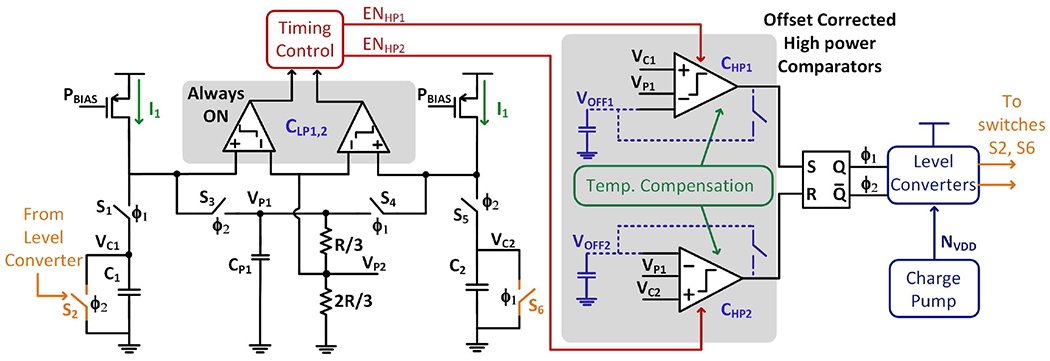
Temperature Compensated RC Oscillator architecture. Switches S2 and S6 are leakage controlled using the negative power supply.
Fig. 3:
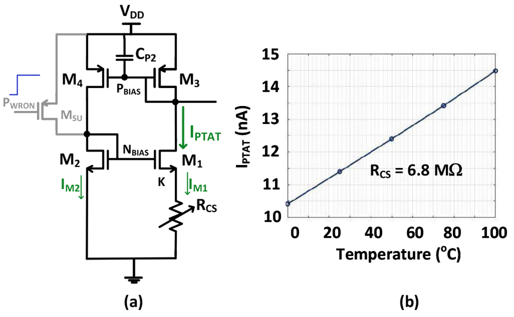
(a) PTAT current source (b) Simulated current waveform for PTAT current source.
Since and ignoring the body effect due to small voltage drop, we can further write the equation as
| (7) |
Therefore, the current in each branch of the current source is given by
| (8) |
where K is set to be 8, and is 5-bit programmable 6.8 polysilicon resistor. The current depends on the thermal voltage, to give a PTAT current source. The simulated current waveform is shown in Fig. 3–(b). We use power-up signal, typically provided by the power management unit during power up, to start-up the current source. Fig. 3–(a) also shows the start-up technique. A low-leakage p-MOS transistor, is added between and . During power-up, is ON to pull the current source away from its other operating point. However, after power up gate of goes to to turn-off this circuit that takes the current source to the correct operating point. To overcome mismatch related issues for the current source, long and wide transistors were used that were carefully laid out using common centroid matching technique.
To achieve low power consumption, the TC-RCO uses four comparators. The resistor used to generate the reference voltage is split into two to generate and , with . The low power comparators are always on. They are used to detect the capacitor voltages crossing . The low power comparator has higher delay but is set to have an earlier trip point of . Once trips, then the higher power comparator is enabled. Since trip point is , or ideally, is on for . Hence, for a 31.6 kHz clock, the high power comparator is enabled for about 5.27 μs before the trip point. The higher delay of does not impact the clock period due to its early trip point. The power consumption reduced is by utilizing low power comparator for larger duration of the clock period and high-power comparator for smaller duration. However, higher performance is maintained by utilizing when the comparator is expected to trip. The high power comparators trip when cross are disabled when to save power. outputs are fed to the Timing Control block which generates the control signals to enable . The Temperature Compensation block and offset correction control the variation of frequency with temperature, and are only used for the high power comparators. The offset correction in the high power comparators is achieved through a negative feedback technique, which is discussed in more detail in Section III-A. The level converter and the charge pump are used to generate a negative bias to control the leakage in switches.
The TC-RCO addresses the nonidealities described in Section II which lead to temperature instability. The oscillator operation is divided into two phases, and is described below.
1). Phase operation:
In phase , switches , and are on, and capacitor is charged from the PTAT current source. Capacitor is discharged to the ground through switch . Comparator is disabled during the entire phase. Phase operation is now further divided into two parts. During (phase ), low power comparator is used to compare and . The low power comparator consumes 23 nW power from a 1V supply, and the high power comparator is disabled. is enabled once trips to save power. The Timing Control Block generates the control signal to enable . In the second part of phase operation (phase ), the comparator senses the voltage , and trips when crosses . The comparator output sets the SR latch, generating the first phase of the clock, which is fed back to control the switches. By using two comparators, the high power comparator is disabled and consumes no quiescent current in phase . The leakage current in the high power comparators is 210pA at 25°C. The reduction in power consumption is greater for higher as is enabled for a shorter duration. In this work,
| (9) |
The offset and delay of the comparator do not contribute to the clock frequency. The offset of the high power comparator is compensated in phase once every four cycles. The delay compensation and offset correction is described in the next section.
2). Phase operation:
Phase operation is symmetrical to phase operation. Switch is now used to generate voltage . Comparator is disabled in the entire phase, and is enabled in . Similar to phase operation, the offset of is compensated once every four cycles during . The comparator output resets the SR latch, generating the second phase of the clock. The two phase operation of the clock helps in achieving 50% duty-cycle for the clock. The additional comparator pair does not increase the power because only one is active in one phase while the other is off. Further, the two phase operation this way averages the current from two current sources, effectively biasing the resistor and charging the capacitor with same current. This eliminates current mismatch related issue in the clock source.
The PTAT current source is used to charge the capacitors and bias the comparators. The PTAT current also generates reference voltage , which also rises linearly with temperature, ignoring the temperature dependence of the resistor itself. Hence, the frequency of oscillation is given by
| (10) |
Since and are both linearly dependent on temperature, is independent of temperature. is generated alternatively through switches and , by the same current sources used to charge the capacitors .
The TC-RCO is operated in two power modes. Since the current generated by the PTAT current source is programmable through , the power consumption and the reference voltage level can be varied. In the low power mode, is set to 12MΩ, with at 110 mV. In high power mode, is decreased, increasing the power consumption. Since is linearly proportional to , varying the bias current does not affect the frequency. and hence, the clock frequency is given by
| (11) |
The simulated waveforms for the TC-RCO are shown in Fig. 4. Table I shows the power breakdown of the TC-RCO sub-circuits in the low power mode. The process variation of the TC-RO can be addressed using conventional calibration methods. The split resistor R can be trimmed without varying the ratio of and to obtain the desired frequency.
Fig. 4:
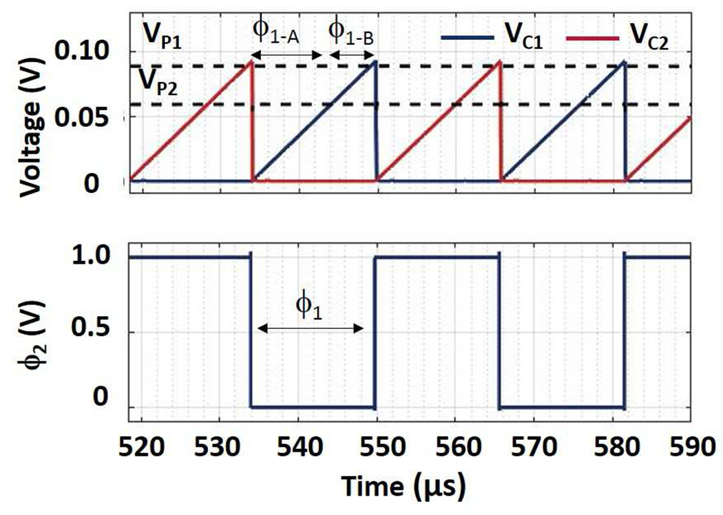
Simulation results showing charging and discharging of capacitors and in the TC-RCO.
TABLE I:
Power Breakdown of Oscillator Sub-Circuits
| Block name | Power (nW) |
|---|---|
| 82 | |
| 46 | |
| Timing Control + Offset correction | 66 |
A. Offset Correction
The offset of the comparator is temperature dependent, leading to a second order temperature instability. The TC-RCO works in two phases, as shown in Fig. 2. The operation of the oscillator in phase is described here. The low power comparator is always enabled. is a low power comparator with a large delay, which senses the capacitor voltage and compares it with . During this time, the high power comparator is disabled, saving power. Once the voltage on the crosses trips, and is enabled. detects crossing . Since the tripping point and delay of is not critical to the frequency, its offset is not corrected. Comparators are designed such that
| (12) |
where is the input offset of the comparators , and .
The complete schematic of the offset corrected comparator is shown in Fig. 5. The offset of is simulated with process and mismatch variation and is shown in Fig. 6. The resistors generating are configurable using 3-bit binary control. For nominal operation, is set to 162 mV, and is set to 108 mV.
Fig. 5:
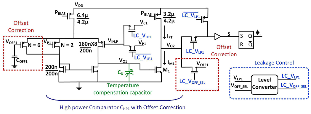
Offset Correction of high power comparator in phase .
Fig. 6:
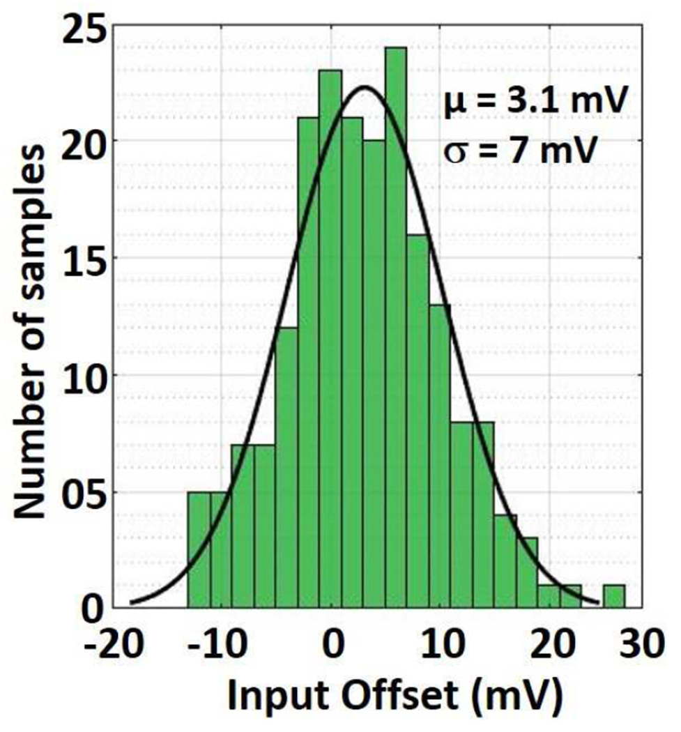
Monte Carlo simulation showing input offset voltage of after 200 runs with process and mismatch variation.
The input offset of is corrected in phase , when . The negative input transistor of the comparator is split into two parallel transistors with and fingers. During offset correction, the positive input transistor is connected to , and the offset storage capacitor is connected in a negative feedback configuration to the input. When there is no mismatch in the comparator, then is equal to . During comparison, the equivalent voltage required for zero output offset is stored on . Once trips, the positive input of is connected to for comparison. Hence, the offset is corrected before starts the comparison operation.
In this operation, the high power comparator is enabled during the entire half cycle. This raises the power consumption of the oscillator. To lower the power consumption, the offset is corrected only once every four cycles. During the first three cycles, is disabled while is in its comparison phase. It is enabled only in phase . In the fourth cycle, is enabled during the entire phase , for correction, and then for comparison. The control signals to enable are generated by the Timing Control Block, shown in Fig. 7. The simulated control signals for are shown in Fig. 8.
Fig. 7:
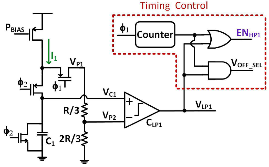
Schematic of TC-RCO in phase showing generation of timing control signals to switch on .
Fig. 8:
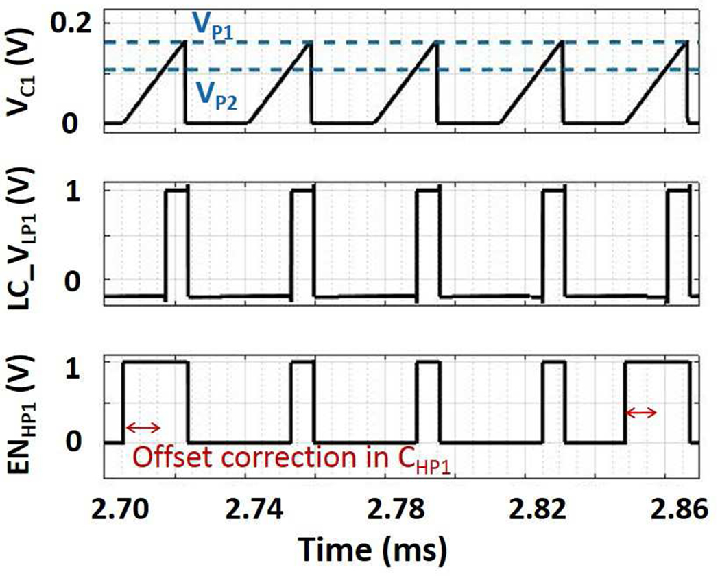
Simulated waveforms showing offset correction of high powered comparator once every four cycles.
B. Leakage Currents in Switches
The leakage current in switches increases exponentially with temperature. The leakage in the switches controlling the offset correction operation directly impacts the frequency of oscillation. The capacitors hold the charge for three consecutive cycles for offset correction. The leakage of switches directly connected to the offset storage capacitor causes to drift. Fig. 9–(a) shows the drift in the voltage of before offset correction is applied with the number of cycles waited for offset correction. Once offset correction is applied, the level of comes back to its initial value. It drifts due to leakage and is brought back to its initial level by offset correction circuit. We chose offset correction after every 4-cycles in the final chip implementation. The error increases as the charge is held for increasing number of clock cycles. In the design implementation of the clock, we selected correcting offset every 4-cycles. Offset correction every 16 cycles shows an addition 7mV drift which can drift the output frequency by about 4%. This would result in a slight reduction in energy per operating frequency. Additionally, the device leakage will play a bigger role in determining the output frequency if offset correction every 16-cycles was performed. We chose offset correction every 4-cycles to reduce the impact of leakage current on output frequency.
Fig. 9:
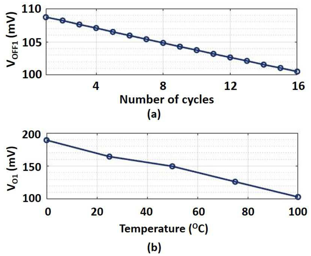
Simulation results showing (a) drift of voltage with number of cycles waited before offset correction and (b) variation of with temperature.
The leakage in the switches is controlled by providing negative gate voltage during the off time of the switches. The negative voltage is generated using a negative voltage charge pump shown in Fig. 10–(a). The charge pump produces a negative voltage of −200 mV, while consuming 5.8 nW power. The negative voltage is provided to a level shifter to generate voltage swing between and . The level shifter schematic is shown in Fig. 10–(b). All switch control signals in the offset correction circuit are first fed to level shifters to generate negative to control switch leakage. The level shifters do not carry steady state DC current, and hence contribute little to the power consumption of the oscillator. Simulation shows a power consumption of 1.1nW for the level shifter at 32 kHz frequency of oscillation. The leakage controlled switches are shown in Fig. 5. All switches are designed with nominal transistors. Fig. 11 shows the oscillation frequency without the generation of . The leakage in the switches rises exponentially with temperature, resulting in an increase in frequency.
Fig. 10:
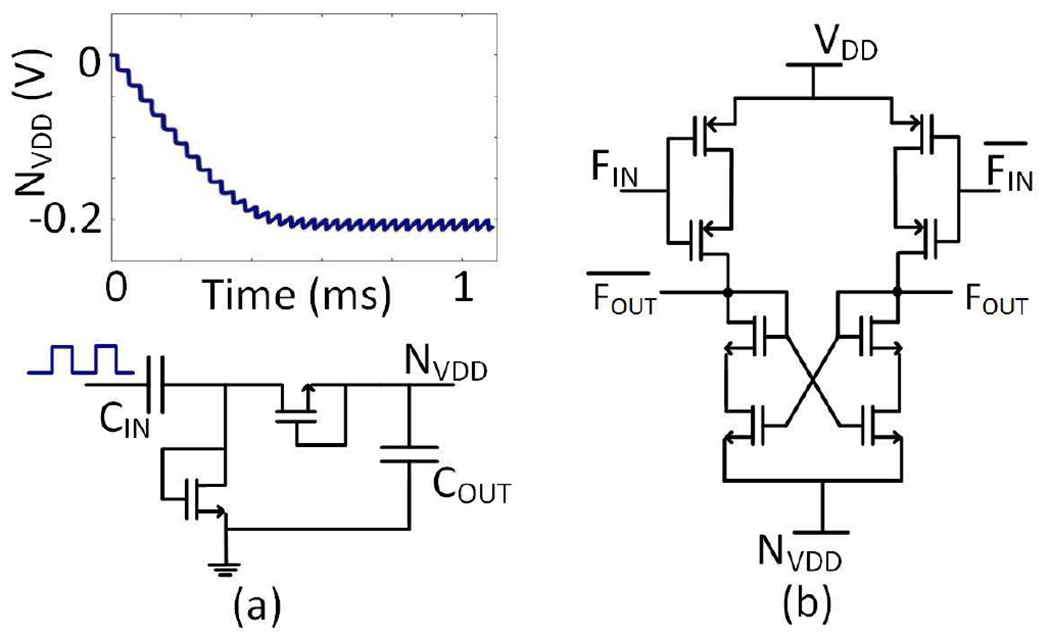
(a) Negative voltage charge pump (b) Level shifter
Fig. 11:
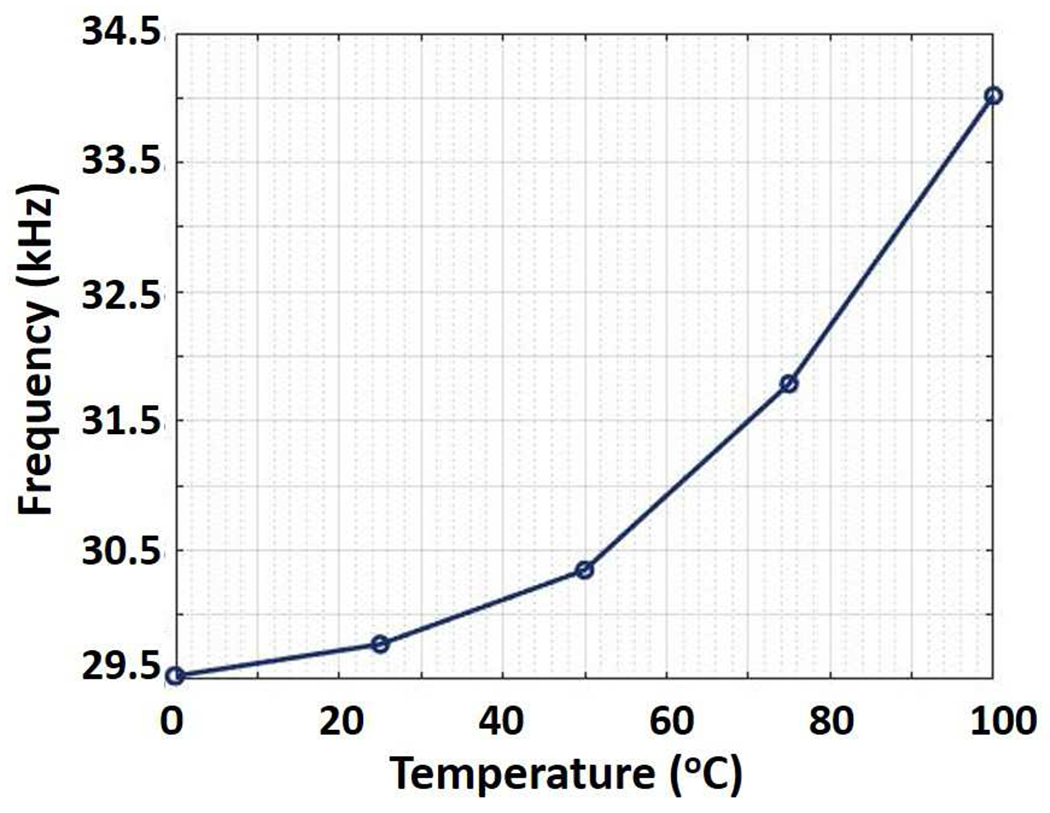
Simulation showing effect of leakage in switches on oscillation frequency.
C. Comparator Delay
The comparator delay directly adds to the time period of the oscillator. Generally, large power comparators are used to make the delay a smaller component of the time period. The delay can degrade the temperature performance of the oscillator as it itself varies with temperature. The low power comparators and do not contribute to the time period of oscillation, and the variation in delay with temperature does not effect the overall temperature stability of the oscillator. The low power comparators have a large delay of 834 ns, while the delay is reduced to 210 ns for the high power comparators . Since voltage is set to be are designed such that
| (13) |
where is the delay of . Hence, only and are compensated for delay variation. Fig. 5 shows the schematic of the high power comparator. The comparator is biased with a PTAT current source. Transistor M1 is biased in the sub-threshold region, such that
| (14) |
where is the sub-threshold saturation current, is the sub-threshold ideality factor, and is the thermal voltage. The comparator trips when , and the tripping point of the comparator is calculated as
| (15) |
2nd-order compensation:
We used n-MOS capacitor as shown in Fig. 5 for 2nd-order compensation. Threshold voltage decreases with increase in temperature. and both increase linearly with temperature, while increases exponentially. Hence, overall, decreases with temperature, resulting in delay of the comparator also decreasing with temperature. The delay of the comparator thus results in a PTAT response in oscillation frequency.
The temperature compensation capacitor gets charged by the differential stage current of the comparator as follows
| (16) |
where for phase operation. is the transconductance of the differential input pair transistors of the comparator, biased in the sub-threshold region.
itself is charged using a PTAT current source , such that
| (17) |
Once reaches , the comparator trips after delay , during which time the capacitor further charges to
| (18) |
| (19) |
| (20) |
| (21) |
Hence, the delay of the comparator is
| (22) |
decreases with temperature, as given in Eq. 15, while rises linearly with temperature. The transconductance of the transistor is constant with temperature as it is biased in the sub-threshold region. Overall, the delay decreases with temperature.
| (23) |
The second factor affecting temperature stability is the variation in resistance R and capacitors and with temperature. R and increase with temperature, resulting in CTAT response in oscillation frequency. Since comparator delay and RC variation show opposing temperature coefficients, their effects can be cancelled out with careful design of the comparator. The delay of the comparator is further increased using an additional MOS capacitor at to achieve 2nd-order compensation. The n-MOS capacitor is biased in positive voltage range where capacitance decreases with voltage. With the rise of temperature, PTAT current increases which decreases discussed above, leading to a reduced load at high temperature. While, the additional capacitor increases the delay of the comparator but it introduces a negative temperature component to cancel out the effect of R and . Further, the dependence of delay on as given by eq. 22 requires that the offset of the comparator needs to be corrected. In the presence of offset, will vary randomly which will reduce the effectiveness of the temperature compensation using the comparator delay. Fig. 12 shows the combined effect of delay and RC variation on frequency of oscillation. The opposing effects of RC and n-MOS varactor cancel out, improving temperature stability to 13 ppm/°C in simulation.
Fig. 12:
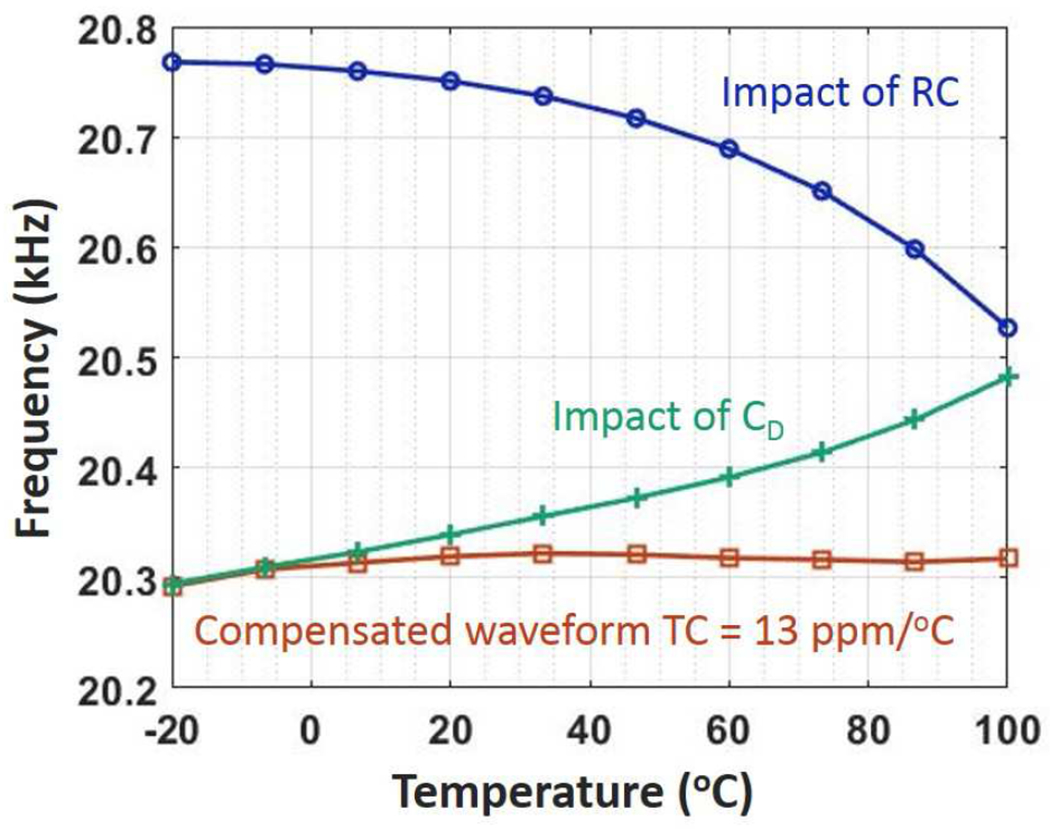
Simulation showing impact of resistor R and NMOS varactor on oscillation frequency.
Fig. 13–(a) shows the variation in frequency of the oscillator with process Monte Carlo variation, with . It shows that our mean frequency of oscillation is 20KHz. Fig. 13–(b) shows the variation of temperature coefficient of the TC-RCO with global process variation. The mean temperature stability is 25 ppm/°C. For this simulation calibration is not used which can improve the temperature stability even for worst corners. Fig. 14 shows the simulated result for frequency variation against temperature for different .
Fig. 13:
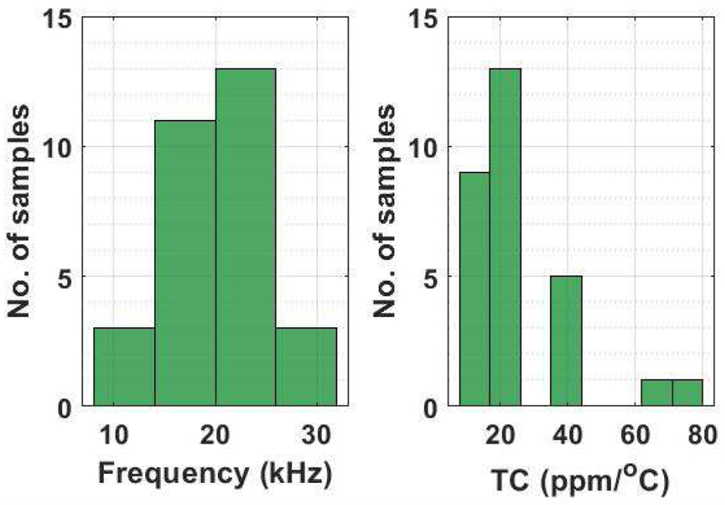
(a) Simulation showing variation of clock frequency with Monte Carlo global process variation for 30 samples, . (b) Simulation showing variation of temperature coefficient with Monte Carlo global process variation for 30 points without calibration.
Fig. 14:
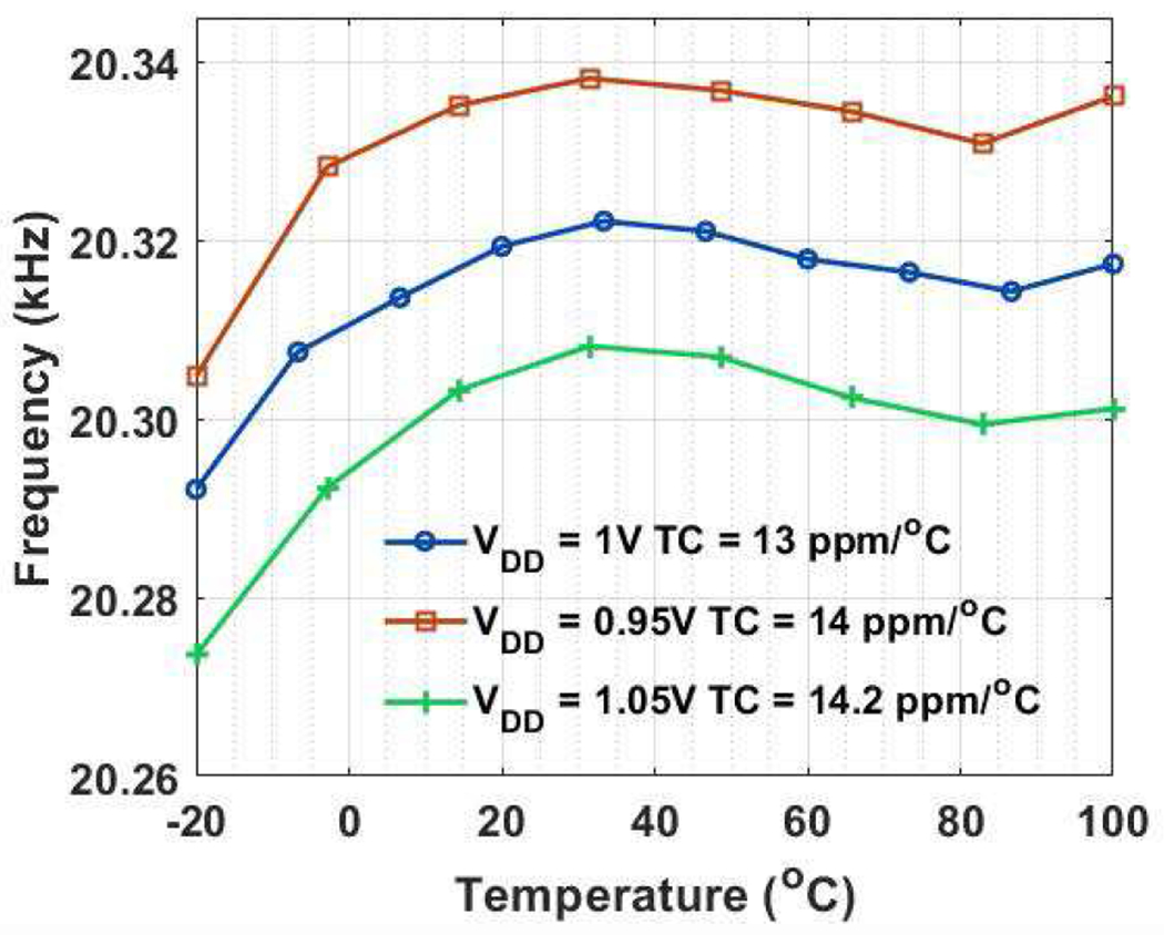
Simulation results showing variation of frequency against temperature for different .
D. Allan Deviation
Noise sources inherent in the oscillator give rise to Allan variance, or long term frequency instability of the oscillator with respect to time. A method to improve the Allan deviation of the RC oscillator is shown here. As shown in Fig. 2, current is used to charge capacitors and . the same current is also used to generate reference voltage . Hence, the frequency of oscillation is given by , which is independent of . However, since , the reference voltage level changes with . Period of oscillation is given by
| (24) |
Owing to the noise generated by the circuit, there will be random variation in the time period . Referring all the noise generated in the circuit to the reference voltage is given by
| (25) |
where is the noise referred to the reference voltage. Therefore, the error in the time period can be given as
| (26) |
For lower , the circuit produces more noise, which implies , where and are the reference voltages for low and high power mode. The low and high power modes differ only in the current value . Comparing the variation in the time period in the low and high power modes,
| (27) |
Hence, the overall randomness around the timing is much lower in the high power mode owing to two factors. First, the higher bias current helps in reducing the input-referred thermal noise of the comparator to reduce overall input noise. Secondly, since the period of oscillation is directly dependent on reference voltage, a higher reference voltage makes noise a lower fraction of the period. These two factors reduce the contribution of noise in the high power mode. This results in a lower Allan deviation in the high power mode. The approach helps in trading off power with long-term instability.
IV. Measurement Results
The TC-RCO was fabricated in 130 nm CMOS process. Fig. 16 shows the die photo, and the area breakdown of the TC-RCO sub-circuits. The total area occupied by the TC-RCO is . The bias current in the high power comparators is also made configurable to effectively cancel out the variation in frequency due to R. The bias current is set only once before the temperature sweep. Fig. 17 shows the variation in frequency with temperature for 4 chips. The four chips achieve temperature stability between 21 ppm/°C and 49 ppm/°C for a temperature range of −20°C to 100°C. Each chip is calibrated only once by configuring the current in the high power comparators to compensate for comparator delay in . The same setting is used for the entire temperature sweep.
Fig. 16:
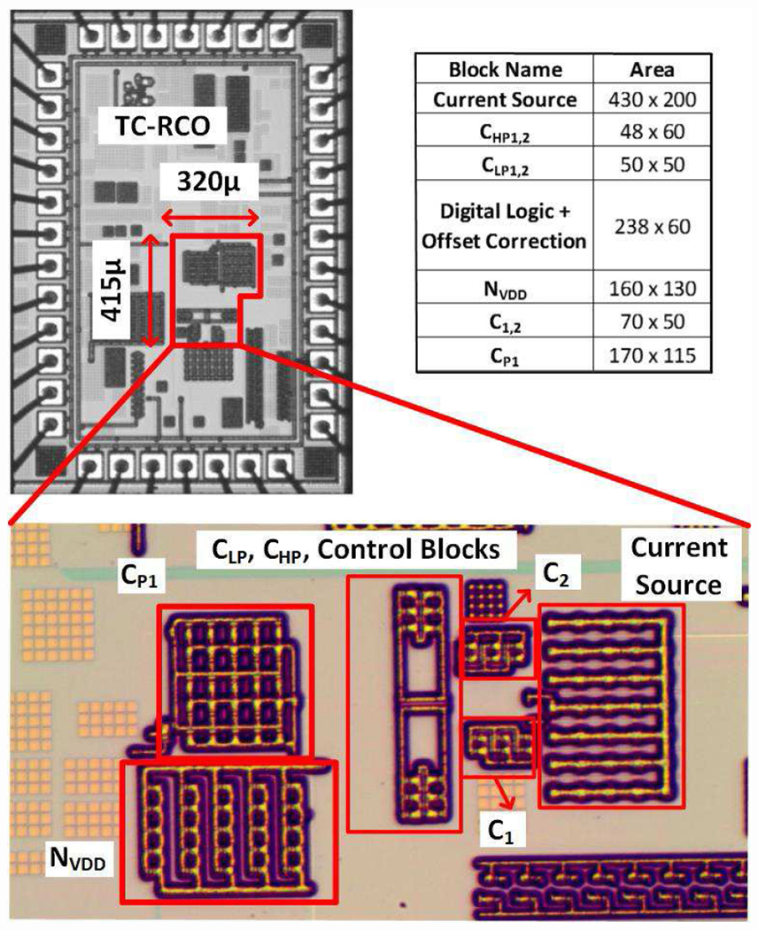
Chip micrograph of TC-RCO.
Fig. 17:
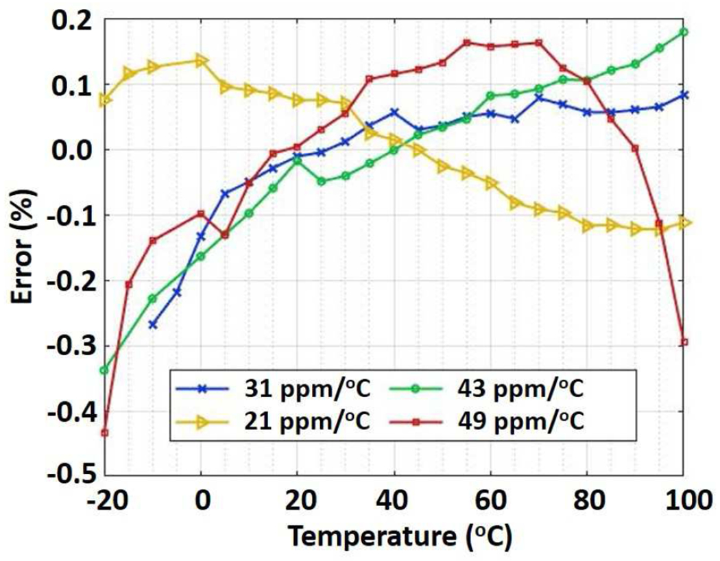
Variation of frequency with temperature for 4 chips. Each chip is calibrated only once to obtain lowest TC.
The supply sensitivity of the oscillator is shown in Fig. 18–(a). The average variation in frequency for 4 chips is 5.5%/V for a supply variation of 0.9 V to 1.3 V. The TC-RCO frequency can be tuned by calibrating the resistor R. Fig. 18–(b) shows the variation in frequency as R is tuned. With 3-bit calibration, the oscillator can be tuned from 18.7 kHz to 21.7 kHz.
Fig. 18:
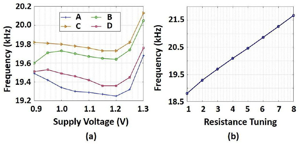
(a) Supply voltage variation of oscillator frequency for 4 chips. The measurement was taken at the lowest power setting with no further calibration.(b) 3 bit calibration of the resistor R for tuning of the RC oscillator.
Fig. 19–(a) shows chip-to-chip variation in frequency, at one process corner, with . It has an average frequency of oscillation of approximately 20KHz which agrees with our simulation results in Fig. 13–a. The TC-RCO was calibrated to be at the lowest power setting, and the variation was found to be 325 Hz with no further calibration for 9 different chips.
Fig. 19:
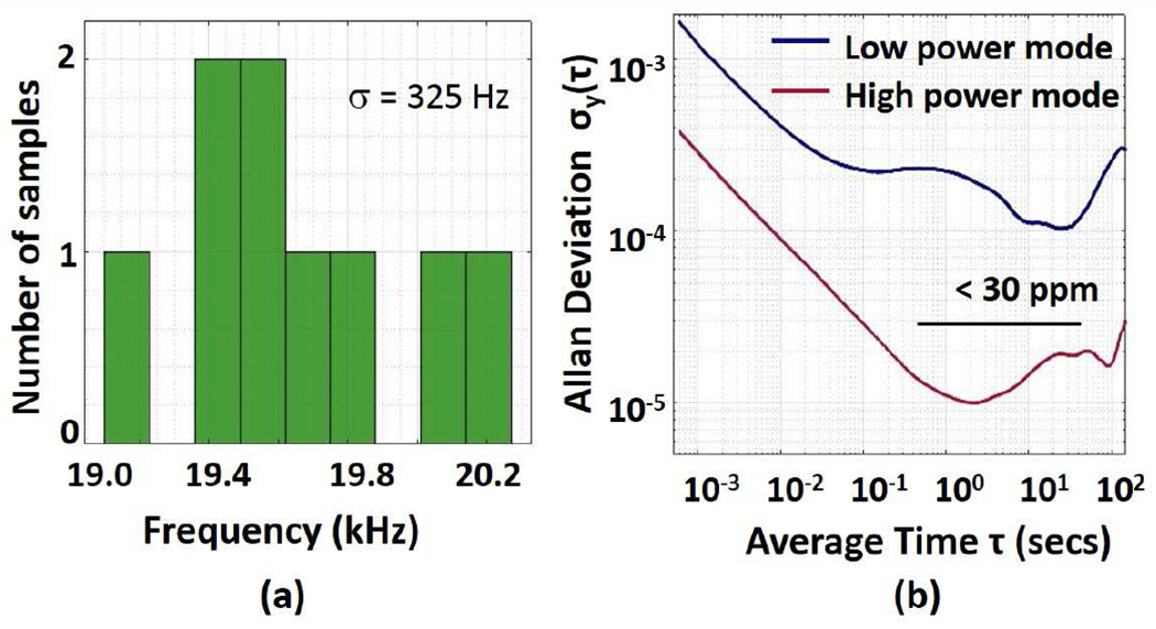
(a)Measured frequency variation of oscillator across 9 chips at room temperature, . The measurement was taken at nominal frequency with no further calibration. (b) Measured Allan Deviation of the TC-RCO.
Table II shows a comparison of performance metrics of the TC-RCO with previously published oscillators. It achieves a minimum temperature stability of 21 ppm/°C and a maximum temperature stability of 49 ppm/°C across 4-different chip for a temperature range of −20-100°C. Oscillator’s minimum temperature stability is one of the lowest for a large temperature range compared to other state-of-the-art oscillators. The TC-RCO also has one of the lowest supply sensitivity a 5%/V variation over a 400 mV range of supply variation. The TC-RCO achieves one of the lowest Allan deviation among oscillators with similar temperature coefficients and temperature range. In this work, we have only used nominal transistors in the TC-RCO design. Previously published state-of-the-art oscillators have been designed with a combination of high transistors (HVT), and low transistors (LVT) to achieve high temperature stability. Overall, the TC-RCO achieves one of the best performance across design parameters. It has one of the lowest TC, supply variation, and Allan Floor with power consumption comparable to other ultra-low power oscillators.
TABLE II:
Performance Summary
| JSSC’16 [9] |
JSSC’18 [12] |
JSSC’16 [17] |
JSSC’19 [18] |
LSSC’19 [19] |
JSSC’20 [20] |
TCSI’19 [21] |
TCSI’19 [22] |
TCSII’18 [23] |
This work | |
|---|---|---|---|---|---|---|---|---|---|---|
| Technology (nm) | 65 | 180 | 180 | 65 | 65 | 65 | 180 | 350 | 65 | 130 |
| Area (mm2) | 0.032 | 0.2 | 0.26 | 0.005 | 0.098 | 0.134 | 0.058 | 0.032 | 0.12 | 0.13 |
| Transistor Type | Nominal Vth HVT |
Nominal Vth DTMOS |
Nominal Vth HVT |
NR | Nominal Vth LVT |
NR | NR | NR | NR | Nominal V th |
| Frequency (kHz) | 18.5 | 1.22 | 70.4 | 1200 | 1016 | 560 | 444.9 | 1000 | 1500 | 20 |
| Power (nW) | 130 | 1.14 | 110 | 820 | 45.3 | 10.5 | 21300 | 160×103 | 6000 | 254/345 * |
| Temp. Range ( ° C) | −40/+90 | −20/+70 | −40/+80 | −25/+125 | −20/+60 | 0/+100 | −20/+100 | −40/+125 | 0/100 | −20/+100 |
| TC (ppm/ ° C) | 27 – 84 | 40 – 153 | 14.7 – 75 | 82 – 113 | 20.3 | 60 – 150 | 224 | 31.5 | 50–100 | 21–49## |
| No. of Chips | 4 | 5 | 5 | 7 | 1 | 4 | 100 | 1 | 4 | 4 |
| Energy (nW/kHz) | 7 | 0.93 | 1.56 | 0.68 | 0.044 | 0.018 | 47.8 | 160 | 4 | 12.8/17.4 |
| Voltage Acc. (%/V) | < 5 | 17.2 | 0.75 | 0.7 | 100 | 11.01 | 0.07 | ±0.08% | 0.15 | 5.5 |
| Allan Floor (ppm) | 20 | 58 | <7 | 10 | 300 | 100 | 1.1 | 15 | NR | 10 @ |
Low Power mode/ High Power mode,
−20-100°C stability in Low Power mode,
Allan floor in High Power mode
The long term stability of the oscillator is measured and shown in Fig. 19–(b). The Allan Deviation is measured at nominal frequency and lowest power settings, and is found to be < 300 ppm after averaging time of 1 s. With increased power from 254 nW to 345 nW, the Allan Deviation floor improves to 10 ppm, showing 30× improvement. The eye diagram of the TC-RCO output is shown in Fig. 20 which shows measured RMS jitter of 390ns which approximately 0.8% of the period. The oscillator output is brought out using 1.6V I/O buffers to protect against electrostatic discharge (ESD) related issues.
Fig. 20:
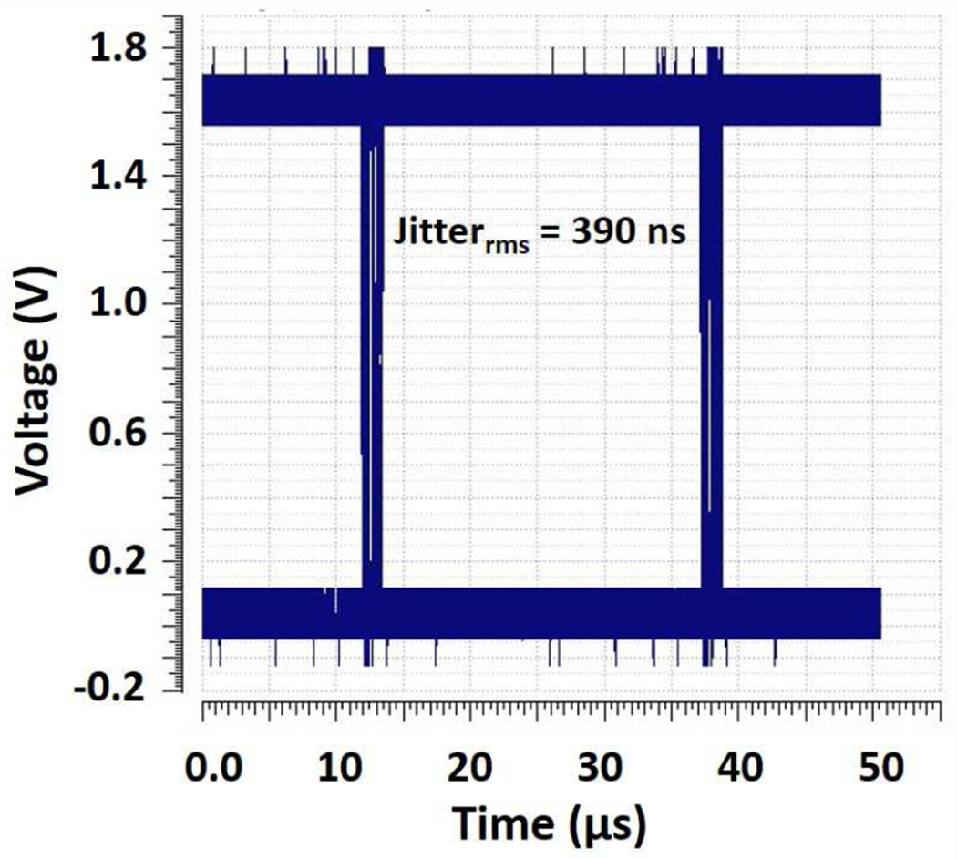
Measured jitter of the TC-RCO.
V. Conclusion
An ultra low power RC oscillator is presented in this work. The TC-RCO achieves high frequency stability by utilizing offset compensation and second order delay compensation in the comparators. The second order compensation is by loading the comparator with an n-MOS capacitor. It achieves a minimum temperature stability of 21 ppm/°C for a temperature range of −20 - 100°C. Additionally, the long term stability of the oscillator is improved with a trade off in power consumption without affecting the oscillator frequency. Long term stability of 10 ppm is achieved after an integration time of 1 sec. The oscillator also achieves low variability with supply voltage, with a voltage accuracy of 5.5%/V. The design is carried out using nominal- transistors and uses a negative supply to control the leakage. It achieves one of the best performance across design parameters for ultra-low power precision clocks.
Fig. 15:
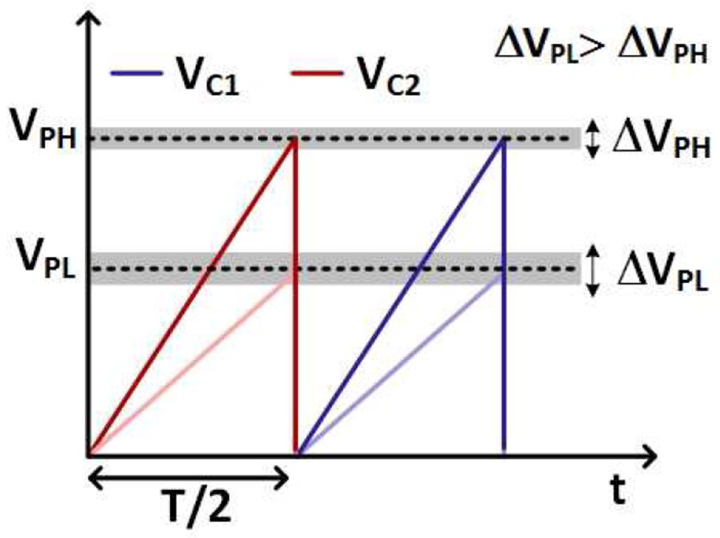
Clock Period at high power and low power mode with noise.
Acknowledgments
This work is supported in part by National Science Foundation (NSF) under grant IIS 2014556, and National Institutes of Health (NIH) under grant HHS/1UF1NS107694-01
Biographies

Nikita Mirchandani (S’17-M’22) received the B.E. (Hons.) degree in electrical and electronics engineering from Birla Institute of Technology and Science (BITS Pilani), India in 2015. She received her M.S and Ph.D. from Northeastern University, MA, USA in 2017 and 2022 respectively. She is currently with ON Semiconductor. Her research interests include the design of low power precision circuits and analog computing hardware for machine learning applications.

Aatmesh Shrivastava (S’12-M’15-SM’19) received his Ph.D. degree from University of Virginia in 2014. Prior to his Ph.D. studies, he worked as a senior design engineer at Texas Instruments, Bangalore from 2006 to 2010. From 2014 to 2016, he worked at the IoT start-up Everactive as senior design director, where he led the research and development of the energy harvesting and power management solutions. In August 2016, he joined Northeastern University, where he is currently working as an Assistant Professor in the Electrical Engineering Department. His research interests include self-powered and ultra-low power circuits and systems, energy-harvesting and analog computing, hardware for AI, internet-of-things, and ultra-low power bio-medical and neural circuits. Dr. Shrivastava is a recipient of 2022 CAREER Award from National Science Foundation (NSF). He currently serves as an Associate Editor for IEEE Transactions on Circuits and Systems Part I: Regular Papers (TCAS-I) and IEEE Open Journal on Circuits and System (OJCAS).
Contributor Information
Nikita Mirchandani, ON Semiconductor, USA.
Aatmesh Shrivastava, Department of Electrical and Computer Engineering, Northeastern University, Boston, MA 02115, USA.
References
- [1].Shrivastava A, Akella Kamakshi D, and Calhoun BH, “A 1.5 nW, 32.768 kHz XTAL Oscillator Operational From a 0.3 V Supply,” IEEE Journal of Solid-State Circuits, vol. 51, no. 3, pp. 686–696, 2016. [Google Scholar]
- [2].Esmaeelzadeh H and Pamarti S, “A Sub-nW 32-kHz Crystal Oscillator Architecture Based on a DC-Only Sustaining Amplifier,” IEEE Journal of Solid-State Circuits, vol. 54, no. 12, pp. 3247–3256, 2019. [Google Scholar]
- [3].Lee Y, Giridhar B, Foo Z, Sylvester D, and Blaauw D, “A 660pW multi-stage temperature-compensated timer for ultra-low-power wireless sensor node synchronization,” in 2011 IEEE International Solid-State Circuits Conference, pp. 46–48, 2011. [Google Scholar]
- [4].Wang H and Mercier PP, “A 51 pW reference-free capacitive-discharging oscillator architecture operating at 2.8 Hz,” in 2015 IEEE Custom Integrated Circuits Conference (CICC), pp. 1–4, 2015. [Google Scholar]
- [5].Asano H, Hirose T, Tsubaki K, Miyoshi T, Ozaki T, Kuroki N, and Numa M, “A 1.66-nW/kHz, 32.7-kHz, 99.5ppm/°C fully integrated current-mode RC oscillator for real-time clock applications with PVT stability,” in ESSCIRC Conference 2016: 42nd European Solid-State Circuits Conference, pp. 149–152, 2016. [Google Scholar]
- [6].Mikulić J, Schatzberger G, and Barić A, “A 1-MHz on-chip relaxation oscillator with comparator delay cancelation,” in ESSCIRC 2017 - 43rd IEEE European Solid State Circuits Conference, pp. 95–98, 2017. [Google Scholar]
- [7].Savanth A, Myers J, Weddell A, Flynn D, and Al-Hashimi B, “5.6 A 0.68nW/kHz supply-independent Relaxation Oscillator with ±0.49%/V and 96ppm/°C stability,” in 2017 IEEE International Solid-State Circuits Conference (ISSCC), pp. 96–97, 2017. [Google Scholar]
- [8].Hsiao K, “A 32.4 ppm/°C 3.2-1.6V self-chopped relaxation oscillator with adaptive supply generation,” in 2012 Symposium on VLSI Circuits (VLSIC), pp. 14–15, 2012. [Google Scholar]
- [9].Paidimarri A, Griffith D, Wang A, Burra G, and Chandrakasan AP, “An RC Oscillator With Comparator Offset Cancellation,” IEEE Journal of Solid-State Circuits, vol. 51, no. 8, pp. 1866–1877, 2016. [Google Scholar]
- [10].Tsubaki K, Hirose T, Kuroki N, and Numa M, “A 32.55-kHz, 472-nW, 120ppm/°C, fully on-chip, variation tolerant CMOS relaxation oscillator for a real-time clock application,” in 2013 Proceedings of the ESSCIRC (ESSCIRC), pp. 315–318, 2013. [Google Scholar]
- [11].Griffith D, Røine PT, Murdock J, and Smith R, “17.8 A 190nW 33kHz RC oscillator with ±0.21% temperature stability and 4ppm long-term stability,” in 2014 IEEE International Solid-State Circuits Conference Digest of Technical Papers (ISSCC), pp. 300–301, 2014. [Google Scholar]
- [12].Jiang H, Wang P-HP, Mercier PP, and Hall DA, “A 0.4-V 0.93-nW/kHz Relaxation Oscillator Exploiting Comparator Temperature-Dependent Delay to Achieve 94-ppm/°C Stability,” IEEE Journal of Solid-State Circuits, vol. 53, no. 10, pp. 3004–3011, 2018. [Google Scholar]
- [13].Ma Y, Cui K, Fang S, and Fan X, “On-chip dual-phase charge-transfer relaxation oscillator with comparator offset cancellation,” Electronics letters, vol. 54, no. 1, pp. 23–25, 2018. [Google Scholar]
- [14].Mikulić J, Schatzberger G, and Barić A, “A 1-MHz on-chip relaxation oscillator with comparator delay cancelation,” in ESSCIRC 2017 - 43rd IEEE European Solid State Circuits Conference, pp. 95–98, 2017. [Google Scholar]
- [15].Dai S and Rosenstein JK, “A 14.4nW 122KHz dual-phase current-mode relaxation oscillator for near-zero-power sensors,” in 2015 IEEE Custom Integrated Circuits Conference (CICC), pp. 1–4, 2015. [Google Scholar]
- [16].Lim Q, Kordesch A, and Keating R, “Performance comparison of MIM capacitors and metal finger capacitors for analog and RF applications,” in 2004 RF and Microwave Conference (IEEE Cat. No.04EX924), pp. 85–89, 2004. [Google Scholar]
- [17].Choi M, Jang T, Bang S, Shi Y, Blaauw D, and Sylvester D, “A 110 nW Resistive Frequency Locked On-Chip Oscillator with 34.3 ppm/°C Temperature Stability for System-on-Chip Designs,” IEEE Journal of Solid-State Circuits, vol. 51, no. 9, pp. 2106–2118, 2016. [Google Scholar]
- [18].Savanth A, Weddell AS, Myers J, Flynn D, and Al-Hashimi BM, “A Sub-nW/kHz Relaxation Oscillator With Ratioed Reference and Sub-Clock Power Gated Comparator,” IEEE Journal of Solid-State Circuits, vol. 54, no. 11, pp. 3097–3106, 2019. [Google Scholar]
- [19].Truesdell DS, Dissanayake A, and Calhoun BH, “A 0.6-V 44.6-fJ/Cycle Energy-Optimized Frequency-Locked Loop in 65-nm CMOS With 20.3-ppm/°C Stability,” IEEE Solid-State Circuits Letters, vol. 2, no. 10, pp. 223–226, 2019. [Google Scholar]
- [20].Truesdell DS, Li S, and Calhoun BH, “A 0.5-V 560-kHz 18.8-fJ/Cycle On-Chip Oscillator With 96.1-ppm/°C Steady-State Stability Using a Duty-Cycled Digital Frequency-Locked Loop,” IEEE Journal of Solid-State Circuits, vol. 56, no. 4, pp. 1241–1253, 2021. [Google Scholar]
- [21].Koo J, Kim B, Park H-J, and Sim J-Y, “A quadrature rc oscillator with noise reduction by voltage swing control,” IEEE Transactions on Circuits and Systems I: Regular Papers, vol. 66, no. 8, pp. 3077–3088, 2019. [Google Scholar]
- [22].Mikulić J, Schatzberger G, and Barić A, “A 1-mhz relaxation oscillator core employing a self-compensating chopped comparator pair,” IEEE Transactions on Circuits and Systems I: Regular Papers, vol. 66, no. 5, pp. 1728–1736, 2019. [Google Scholar]
- [23].Wang T, Griffith D, Ahmed MG, Zhu J, Wei D, Elkholy A, Elmallah A, and Hanumolu PK, “A 6 μ w ±50 ppm/°c ±1500 ppm/v 1.5 mhz rc oscillator using self-regulation,” IEEE Transactions on Circuits and Systems II: Express Briefs, vol. 66, no. 8, pp. 1297–1301, 2019. [Google Scholar]


