

Summary
Flexible perovskite solar cells (PSCs) are highly promising photovoltaic technologies due to the prospect of integration with wearable devices. However, conventional encapsulation strategies for flexible devices often cause secondary damage to the perovskite crystals, which affects device performance. Here, we present self-encapsulated flexible PSCs realized by lamination technology. The conversion of perovskite crystals is achieved by the diffusion of lead iodide and ammonium halide under the effect of temperature and pressure. In addition, the hydrogen bonding of the introduced polyacrylamide enhances the connections of the integral device while improving the crystal quality. The self-encapsulated flexible PSCs achieve an outstanding photovoltaic conversion efficiency of 22.33%, and comprehensive stability tests are conducted based on wearable device application scenarios to verify the feasibility. Finally, 25 cm2 wearable perovskite modules are successfully applied into the neuro-assisted wearable devices.
Subject areas: Materials characterization, Materials processing, Optical materials
Graphical abstract
Highlights
-
•
Self-encapsulated flexible PSCs are realized by lamination technology
-
•
Polyacrylamide is introduced as a binder to improves the crystalline quality
-
•
Self-encapsulated flexible PSCs achieve an outstanding PCE of 22.33%
-
•
Wearable perovskite modules are applied into the neuro-assisted wearable devices
Materials characterization; Materials processing; Optical materials
Introduction
In recent years, solar cells have attracted the attention of researchers as the backbone of renewable energy technology. Compared with conventional crystalline silicon and inorganic thin-film solar cells, perovskite solar cells (PSCs) have high defect tolerance, high light absorption coefficient, and low cost.1,2,3,4 More importantly, PSCs can be prepared by solution processing to be compatible with flexible device applications.5,6,7 However, the premise of flexible device applications is encapsulation accompanied by a non-significant loss of photovoltaic conversion efficiency (PCE). In particular, most of the current encapsulation strategies for flexible devices are achieved by heating or ultraviolet curing of the flexible substrate, which is inevitable for the damage to the original perovskite crystal.8 Therefore, avoiding damage to the perovskite light-absorbing layer while achieving flexible device encapsulation and further verifying the wearable applications are critical to the commercial feasibility of flexible PSCs.
Conventional flexible device fabrication processes involve the deposition of transparent conductive electrodes on substrates of poly(ethylene terephthalate) (PET) or poly-ethylenenaphthalate (PEN), followed by the sequential deposition of multifunctional layers and the vaporization of metal electrodes to achieve a complete device structure.9,10,11 Flexible PSCs have evolved rapidly over the past decade, and the flexible PSCs are based on interface engineering, electrode design, and crystal quality optimization achieving a soaring PCE from the first reported value of 2.62%–23.6%, demonstrating the great potential for future integration into wearable devices.12,13,14,15,16 To further broaden the application scenario of flexible PSCs, recently, ultra-thin solar cells based on micron-scale PET and parylene derivative substrates have emerged, demonstrating extremely high power per weight.17,18 However, for flexible PSCs with conventional device structures, additional encapsulation steps are essential, which makes the maintenance of high-quality perovskite crystals challenging. Therefore, simple and efficient encapsulation strategies for flexible PSCs need to be further investigated to meet the needs of flexible applications. Recently, the optimizations of perovskite crystal quality by lamination process have been well documented.19,20,21,22,23 The recrystallization process of perovskite crystals can be induced under specific temperature and pressure. Therefore, there is significant potential to consider the integration of dual-sided flexible substrates through lamination technology, combined with the barrier to external water and oxygen, to achieve excellent encapsulation.
In this work, we report a simple and effective lamination strategy for flexible PSCs encapsulation. By depositing different functional layers on each of the two PEN/indium tin oxide (ITO) transparent electrodes, lead iodide and metal salts come into direct contact. The organic cationic salt diffuses to the lead iodide side to form perovskite crystals under the lamination process. To further enhance the adhesion between the sub-cells, polyacrylamide (PAM) is introduced as a binder, which simultaneously improves the crystalline quality. Finally, the self-encapsulated flexible PSCs exhibit an outstanding PCE of 22.33% and maintain 83% of the initial efficiency under 8,000 bending cycles at a curvature radius of 5 mm. It is worth noting that comprehensive stability tests are conducted for wearable device application scenarios. The initial efficiencies of 88% and 91% are maintained after 1-sun illumination for 1,000 h and storing at 35°C (40 ± 5% relative humidity) for 1,000 h, respectively. This lamination strategy provides a novel idea for simple and efficient encapsulation of flexible PSCs.
Results and discussion
These ultra-flexible PSCs are realized by lamination of front stack structure of PEN/ITO/SnO2/PbI2 and back stack structure of PEN/ITO/PTAA (poly(bis(4-phenyl)-2,4,6-trimethylphenylamine))/ammonium halide. To further enhance the stability of the device structure after lamination, PAM is introduced as a binder. As shown in Figures 1A–1E and S1, the PbI2 and ammonium halide are deposited on the SnO2 and PTAA surfaces, respectively. Subsequently, the PbI2 and ammonium halide are diffused under both heating and pressure to form perovskite crystals. At the same time, the reinforcement of the device structure is realized due to the hydrogen bonds of the amide group in the PAM molecule, and a combination test (Figure S2) between the upper and lower sub-cells is used to verify this idea. This simple and effective encapsulation strategy enables the diffusion growth of perovskite crystals, thus avoiding crystal damage and defect formation caused by additional treatment processes.
Figure 1.

Schematic diagram of ultra-flexible PSCs device is realized by lamination of front stack structure of PEN/ITO/SnO2/PbI2 and back stack structure of PEN/ITO/PTAA/ammonium halide
(A–E) (A) Deposition of precursors of PbI2, (B) front stack structure of PEN/ITO/SnO2/PbI2, (C) Deposition of organic cationic salts, (D) back stack structure of PEN/ITO/PTAA/ammonium halide, and (E) The perovskite crystals are formed by thermal diffusion during the lamination process, and PAM realizes the adhesion between the sub-cells. See Video S1 in supporting information for the full procedure.
To reveal the critical role of the PAM in modulating the crystal growth, the morphology of perovskite films doped with different contents (0.01 wt %, 0.03 wt %, and 0.05 wt %) of PAM has been further observed. The laminated flexible PSCs are mechanically peeled, and scanning electron microscopy (SEM) measurements are conducted (Figures 2A–2D). It can be observed clearly that the grain size of the control film is mostly less than 100 nm, and there exist a substantial number of pinholes on the surface. When 0.01 wt % of PAM is introduced, this phenomenon is significantly improved, and some of the crystals grow to micron size, while most of the holes are eliminated. By continuing to increase the doping content to 0.03 wt %, the crystal growth is more adequate and most of the grain size distribution above the micron level is obtained. When the doping content is further increased to 0.05 wt %, irregular textures as well as blurred grain boundaries start to appear on the surface of the perovskite films. It is hypothesized that the introduction of too much PAM has a negative effect on the crystal growth, and the insulating property of the polymer itself has an influence on the SEM images. Meanwhile, SEM images (Figure S3) of the surface morphology of SnO2 side synchronously verify that the introduction of PAM avoids crystal rupture during peeling. Based on the morphology evolution of the perovskite films, it is not difficult to conclude that the introduction of PAM is conducive to the improvement of the quality of crystal growth. We speculate that during the lamination-induced diffusion growth, the C=O in the amide group will coordinate with Pb2+ to improve the crystallinity of the perovskite films and passivate the grain boundaries.24 Therefore, X-ray photoelectron spectroscopy (XPS, Figure S4) tests are performed to evaluate the interaction between PAM and perovskite crystals. When PAM is introduced, the binding energy of Pb 4f shows a significant shift, indicating that the chemical environment of Pb element has changed, which verifies the previous speculation. Meanwhile, the N-H in the amide group will further form hydrogen bonding with the iodide ion in [PbI6]4-, and the two will synergistically regulate the suppression of Pb/I-related defects on the surface of the perovskite films for more adequate crystal growth.25
Figure 2.

Morphology analysis of perovskite films
(A–D) SEM images of (A) control, (B) 0.01 wt %, (C) 0.03 wt %, and (D) 0.05 wt % PAM-doped films, the scale bar in images is 1 μm.
Subsequently, X-ray diffraction (XRD) measurements are performed to further examine the crystalline quality of perovskite films with different content of PAM. As shown in Figure 3A, the intensity of the α-phase characteristic peak corresponding to 14° gradually increases with an ascending content of PAM, indicating the increased crystallinity of the perovskite crystals. However, when the additive content is further increased to 0.05 wt %, the PbI2 characteristic peak (11.5°) appears, suggesting the excess PAM has a negative effect on the crystallization process, which is in consistent with the previous SEM results. Therefore, 0.03 wt % is verified as the optimal ratio for PAM doping and subsequent comprehensive experiments. For convenience, PAM-doped samples of 0.03 wt % are defined as the target. The superiority of the PAM doping strategy is further verified by investigating the optical properties of the perovskite films. The ultraviolet-visible (UV-vis, Figure 3B) spectrum and steady state photoluminescence (PL, Figure 3C) tests show that the absorption intensity and the fluorescence emission peak intensity of the target sample increased significantly, indicating the improved quality of the perovskite crystals and the suppressed nonradiative recombination.26 Meanwhile, time-resolved PL (TRPL, Figure 3D) tests are further performed, and the carrier lifetime of the target sample reached 238.41 ns, which is higher than that of the control sample of 138.86 ns. The improved carrier lifetime indicates that the carrier trapping due to surface defects is effectively suppressed, favoring improved carrier transport dynamics.27
Figure 3.

Analysis of perovskite crystal quality
(A) XRD patterns of perovskite films with different PAM doping amounts.
(B–D) (B) UV-Vis, (C) PL, and (D) TRPL spectrum of the control and target films.
In order to further understand the semiconductor performance of perovskite films, the density of defect states (Nt) is tested by the space charge-limited current (SCLC) method in Figure 4A. The formula of Nt is defined as follows28:
where e represents the elementary charge, L corresponds to the thickness of the perovskite film, ε is the relative dielectric constant, ε0 represents the vacuum dielectric constant, and VTFL is the trap-filled limited voltage. According to the calculation, the VTFL of control and target samples is 0.319 V and 0.247 V, respectively, and the corresponding Nt is 1.46×1016 cm−3 and 1.13×1016 cm−3, respectively. These values are at the same level as those currently reported for the formamidinium iodide (FA)-based polycrystalline perovskite films, which shows that doped PAM can effectively passivate perovskite crystals, thus inhibiting the generation of defects. Subsequently, the carrier transport dynamics are measured to verify the effect of PAM doping. Through the transient photocurrent (TPC, Figure 4B) and transient photovoltage (TPV, Figure 4C) tests, it can be found that the target sample has smaller carrier extraction time (0.2 μs) and longer carrier recombination time (1.32 ms), when compared with the control sample (0.43 μs and 1.03 ms), suggesting a more efficient carrier extraction and transport process.29
Figure 4.

Semiconductor properties measurement of flexible PSCs
(A) The SCLC curves indicating the trap-filling limited voltage (VTFL) and the trap density (Nt) of control and target devices.
(B and C) (B) Transient photocurrent and (C) transient photovoltage of control and target devices.
(D and E) The light-intensity-dependent (D) current density and (E) voltage properties of control and target devices.
(F) The electrochemical impedance spectroscopy properties of the control and target devices.
Then, the power-law dependence of short-circuit current density (JSC) and light intensity (JSC ∝ I α) is explored to verify the space charge effect in Figure 4D. In general, if the mobility difference between electrons and holes is small, a single charge will not accumulate excessively, thus avoiding the space charge effect.30 The α values of control and target samples are 0.947 and 0.948, respectively, suggesting a similarly balanced carrier transport in both samples. However, the slope of the open-circuit voltage (VOC) versus light intensity decreases from 2.18 KBT/q to 1.46 KBT/q after the PAM doping in Figure 4E. This deviation from the ideal factor of 1 is often caused by nonradiative recombination;31,32,33 therefore nonradiative recombination in the target sample with a smaller slope is significantly suppressed, which facilitates the increase of VOC. Carrier transport and recombination behavior is further investigated by electrochemical impedance spectroscopy (EIS, Figure 4F) measurements. By fitted equivalent circuit model, it is found that there is a greater charge-recombination resistance in the target device, which is conducive to inhibiting carrier recombination, and this favors the improvement of the fill factor (FF). Meanwhile, dark current test (Figure S5) results are fitted by single PN junction model,34 which was divided into three areas, A, B, and C, related to shunt current, recombination current, as well as diffusion current, respectively. The reduced recombination current and the increased diffusion current in the target devices are crucial for the enhancement of device performance.
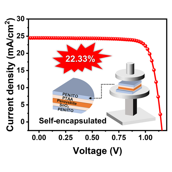
By employing this lamination design, we tested the device performance of self-encapsulated flexible PSCs as shown in Figure 5A and S6. Based on the structure of PEN/ITO/SnO2/Perovskite/PTAA/ITO/PEN, the target device shows an outstanding PCE of 22.33% with a VOC of 1.15 V, an FF of 79.45%, and a JSC of 24.49 mA/cm2, which also exhibits negligible performance differences from both sides (Figure S7). Compared to the control device with a VOC of 1.06 V, an FF of 64.83%, and a JSC of 21.47 mA/cm2, the performance parameters as well as the reproducibility (Figure S8) of the target devices have been significantly improved after the PAM doping. It is noteworthy that all JSC are consistent with the values integrated from the external quantum efficiency (EQE, Figure S9) spectra. It is presumed that the significantly improved device performance parameters are attributed to the improved perovskite crystal quality and the optimized carrier transfer and recombination behavior. Meanwhile, Forward and reverse scanning current density-voltage (J-V) curves (Figure S10) further verify the weakened hysteresis effect in target devices. To confirm the feasibility of self-encapsulated flexible PSCs in wearable devices, the device stability is thoroughly tested for different application scenarios. First, operational stability is tested for 300 s at maximum power point tracking (Figure S11), and the target device exhibits a smaller current variation compared to the control device, demonstrating the critical role of PAM in device stability. The bending cycles under different bending radii (R) are tested, where R = 5 mm and R = 3 mm are shown in Figures 5B and S12, respectively. After 8,000 cycles with 5 mm, the target device can still maintain 83% of the initial efficiency. However, the performance of the control device has declined to 20% of the initial efficiency after 6,500 cycles. When the bending radius is further reduced to 3 mm, after 5,000 cycles, the target device and control device maintain 81% and 31% of the initial efficiency, respectively. The results show that PAM as a binder plays a significant role in improving the quality of perovskite crystal and the mechanical stability of flexible PSCs. It is hypothesized that the flexible substrate thickness will dominate compared to the nanoscale thickness of the perovskite layer, thus placing the perovskite layer in a transition layer, also known as a stress-neutral layer. This mechanical structure allows the perovskite layer to be subjected to less stress, thus effectively releasing the stress accumulation.
Figure 5.

Device performance and stability of flexible PSCs
(A) Current density-Voltage curves of the control and target devices.
(B–D) Normalized average PCE of the control and target devices as a function of bending cycles with R = 5 mm. Normalized average PCE of the control and target devices as a function of time with (C) 1-sun illumination and (D) heating at 35°C (40 ± 5% relative humidity), where RH is an abbreviation for relative humidity.
(E) Performance of 25 cm2 wearable perovskite power source.
(F) Biomedical application of the wearable perovskite power source on the deep brain stimulation.
Subsequently, the long-term stability of the device under different environments is further verified. The target device maintains 88% of the initial PCE after 1,000 h of 1-sun light exposure in Figure 5C, while the control device declines sharply to 11% of the initial PCE. Meanwhile, the thermal stability of the devices is evaluated. After heating at 75°C (40 ± 5% relative humidity, Figure S13) for 800 h, the performance of the target device maintains a considerably initial PCE of 85%, while the target sample could only retain 31% of the initial PCE. Then, the stability of the device is tested based on the human body temperature under normal- (40 ± 5% relative humidity, Figure 5D) and high-humidity (80 ± 5%, Figure S14) environment. It can be seen that the target device maintains 91% of the initial PCE after 1,000 h of heating at 35°C (40 ± 5% relative humidity), compared to only 25% of the initial performance of the control device, indicating that the PAM-doped device is more stable. Even after 800 h at high humidity (80 ± 5%), 87% of initial efficiency is maintained. This phenomenon suggests that PAM acts as a binder while improving the quality of perovskite crystals, which is essential for the stability enhancement of self-encapsulated flexible PSCs.
In order to further verify the advancement of the strategy, we further prepared 25 cm2 wearable perovskite photovoltaic power supply. Notably, as shown in Figure 5E, the wearable perovskite photovoltaic power supply shows a PCE of 10.18% with a VOC of 4.84 V, which means that can be used to power commonly used wearable electronic devices. Therefore, we continue to apply wearable electronic devices in the study of enhanced battery life of biomedical devices. The deep brain stimulation (DBS) has been widely used in the adjuvant therapy of various neurological diseases.35,36 The capacity of its battery is one of the problems limiting its popularization. We combined the wearable PSCs with DBS technology and found that it could meet the electrical compatibility of the device (Figure 5F), which means that the self-encapsulated wearable power supply has a very wide range of applications.
Conclusions
Self-encapsulated flexible PSCs are fabricated by lamination process, and the conversion of PbI2 and ammonium halide into perovskite crystals is achieved by diffusion process under the effect of pressure and temperature. In particular, the introduction of PAM as a binder improves the crystalline quality of the perovskite crystals while reinforcing the integral device structure. The carrier extraction and transport are improved by suppressing the defect formation and carrier recombination behavior. Finally, the flexible PSCs obtained an outstanding PCE of 22.33%, and comprehensive stability tests are conducted to verify the feasibility under wearable device application scenarios, further demonstrating the stability gain from the introduction of PAM. Moreover, 25 cm2 wearable perovskite photovoltaic is successfully applied into the neuro-assisted wearable devices. This approach provides a new idea for simple and efficient encapsulation of flexible PSCs.
STAR★Methods
Key resources table
| REAGENT or RESOURCE | SOURCE | IDENTIFIER |
|---|---|---|
| Chemicals, peptides, and recombinant proteins | ||
| Tin(Ⅳ) oxide (SnO2) | Alfa-Asear | CAS: 18282-10-5 |
| Polyacrylamide (PAM) | Sigma-Aldrich | CAS: 9003-05-8 |
| N, N-dimethylformamide (DMF) | Sigma-Aldrich | CAS: 68-12-2 |
| Dimethyl sulfoxide (DMSO) | Sigma-Aldrich | CAS: 67-68-5 |
| Isopropanol (IPA) | Sigma-Aldrich | CAS: 67-63-0 |
| Poly[bis(4-phenyl) (2,4,6-trimethylphenyl) amine] (PTAA) | Xi’an p-OLED | CAS: 1333317-99-9 |
| Formamidinium iodide (FAI) | Xi’an p-OLED Xi’an p- | CAS: 879643-71-7 |
| Methanaminium bromide (MABr) | OLED | CAS: 6876-37-5 |
| Methylammonium chloride (MACl) | Xi’an p-OLED | CAS: 593-51-1 |
| Lead (II) iodide (PbI2) | Xi’an p-OLED | CAS: 10101-63-0 |
Resource availability
Lead contact
Further information and requests for resources should be directed to and will be fulFIlled by the lead contact, Professor Meng Su (sumeng1988@iccas.ac.cn).
Materials availability
This study did not generate new materials.
Experimental model and subject details
This work did not need any unique experimental model.
Method details
Experimental procedures
Fabrication of PSCs
First, the flexible PEN/ITO substrates were cleaned by isopropyl alcohol for 15 min and then dried with a nitrogen stream. Then, the pre-cleaned PEN/ITO substrates were treated by ultraviolet (UV)-ozone for 5 min in UV chamber. The SnO2 was spin-coated on the PEN/ITO substrates at 3000 rpm for 30 s, annealing at 130°C for 30 min. The PbI2 solution was prepared by dissolving PbI2 (691.5 mg) in 1 mL anhydrous DMF/DMSO mixture solvent (9/1, v/v) under N2 condition, and the solution was stirred at 60°C for 10 h and filtered. The mixture of PbI2 and PAM is prepared in advance for spin-coating. The 50 μL PbI2 solution was spin-coated onto the SnO2 substrates at 1500 rpm for 30 s and the substrates were subsequently annealed at 70°C for 1 min. Then, another pre-cleaned PEN/ITO substrates were treated by ultraviolet (UV)-ozone for 5 min in UV chamber. The PTAA (3 mg/mL in CB) was spin-coated on the PEN/ITO substrates at 6000 rpm for 30 s, annealing at 100°C for 10 min. Then, the mixture solution was prepared by dissolving a mixture of FAI (90 mg), MABr (9 mg) and MACl (9 mg) in 1 mL IPA, and the solution was stirred at 25°C for 5 h and filtered. The 50 μL mixture solution was spin-coated onto the PTAA substrates at 2000 rpm for 30 s and the substrates were subsequently annealed at 130°C for 15 min. The final devices were fabricated by laminating the front and back stacks with a temperature controllable laminator. The optimum lamination temperature of 120°C is carried out and lamination pressure is 30 bar for 20 min. The active area of this device was fixed at 0.04 cm2, where the effective area of the small device is determined by the overlapping area of the two sub-cell electrodes crossed.
Fabrication of perovskite solar modules
For perovskite modules, the two substrates are respectively marked by laser etching before fabricating the sub-cells. Then, the two substrates are coated with PbI2 and cationic salt, respectively, and marked by second etching. In order to ensure good connection between each sub-cell, we widen the width of the second etching and introduce conductive silver glue to ensure good contact between the adjacent sub-cell electrodes. After that, the modules are fabricated by aligning and laminating each effective region of the two sub-cells. Module geometry filling is 80%, a total of five sub-cells, through the upper and lower laminating to achieve the series of sub-cells.
Film characterizations
The morphology of films is measured by SEM (JEOL, JSM-7500F,104 Japan) at an accelerating voltage of 5.0 kV. The 105 ultraviolet-visible (UV-Vis) spectra are recorded by SHIMADZU, UV-2600 spectrophotometer. The photoluminescence (PL) spectra and time-resolved photoluminescence (TRPL) spectra at the peak emission of ∼800 nm are measured by photoluminescence spectroscopy (FLS920, Edinburgh Instruments Ltd.). The TRPL excitation fluence is about 4 nJ cm−2 from a 405 pulsed laser with a wavelength of 405 ± 8 nm and pulse width of 45 ps, at a repetition rate of 0.1 MHz. The PL decay data is recorded using time-correlated single photon counting technique. Grazing incidence X-ray diffraction (GIXRD) measurements are recorded by D8-Discover 25 diffractometer (Bruker). The electrical impedance spectroscopy (EIS) is performed with Zahner electrochemical workstation.
Solar cells characterizations
The current density-voltage (J-V) and current-voltage (I-V) curves are characterized using Keithley 2400 Sourcemeter. The currents are measured under the solar simulator (Enli Tech, 100 mW cm−2, AM 1.5G irradiation) and the reference silicon solar cell is corrected from NREL. All the measurements are performed under nitrogen at room temperature. The reverse scan range is from 1.2 V to 0 V and the forward scan range is 0 V–1.2 V, with 8.0 mV for each step, the scan rate is 0.2 V s−1, the delay time is 30 ms.
Quantification and statistical analysis
We report the average photovoltaic parameters and standard deviations to compare solar cell performance under the same standard test conditions. We also provide a statistical analysis of power conversion efficiency on 20 different samples fabricated with the same procedure.
Acknowledgments
This research was funded by the National Natural Science Foundation of China (NSFC) (52222312, 22005131, 52173169), the Natural Science Foundation of Jiangxi Province (20212BAB214055, 20224ACB204007), and the "Double Thousand Plan" Science and Technology Innovation High-end Talent Project of Jiangxi Province (jxsq2019201049).
Author contributions
G. S. and X. H. conceived and designed the experiments. T. X. and R. Z. fabricated the PSCs devices. Z. C. and M. S. characterized and analyzed the device performance and morphology of PSCs. T. X., R. Z., and X. H. characterized and analyzed the various photoelectric properties. D. W. and G. S. completed the writing of the manuscript.
Declaration of interests
The authors declare no competing financial interests.
Published: June 28, 2023
Footnotes
Supplemental information can be found online at https://doi.org/10.1016/j.isci.2023.107248.
Contributor Information
Meng Su, Email: sumeng1988@iccas.ac.cn.
Xiaotian Hu, Email: happyhu@ncu.edu.cn.
Guochen Sun, Email: sgc3130@126.com.
Supplemental information
Data and code availability
-
•
Data: All data reported in this paper will be shared by the lead contact upon request.
-
•
Code: This paper does not report original code.
-
•
Any additional information required to reanalyze the data reported in this paper is available from the lead contact upon request.
References
- 1.Jiang Q., Tong J., Xian Y., Kerner R.A., Dunfield S.P., Xiao C., Scheidt R.A., Kuciauskas D., Wang X., Hautzinger M.P., et al. Surface reaction for efficient and stable inverted perovskite solar cells. Nature. 2022;611:278–283. doi: 10.1038/s41586-022-05268-x. [DOI] [PubMed] [Google Scholar]
- 2.Wang R., Xue J., Wang K.-L., Wang Z.-K., Luo Y., Fenning D., Xu G., Nuryyeva S., Huang T., Zhao Y., et al. Constructive molecular configurations for surface-defect passivation of perovskite photovoltaics. Science. 2019;366:1509–1513. doi: 10.1126/science.aay9698. [DOI] [PubMed] [Google Scholar]
- 3.Xing Z., An M.-W., Chen Z.-C., Hu M., Huang X., Deng L.-L., Zhang Q., Guo X., Xie S.-Y., Yang S. Surface Re-Engineering of Perovskites with Buckybowls to Boost the Inverted-Type Photovoltaics. J. Am. Chem. Soc. 2022;144:13839–13850. doi: 10.1021/jacs.2c05235. [DOI] [PubMed] [Google Scholar]
- 4.Li Z., Li B., Wu X., Sheppard S.A., Zhang S., Gao D., Long N.J., Zhu Z. Organometallic-functionalized interfaces for highly efficient inverted perovskite solar cells. Science. 2022;376:416–420. doi: 10.1126/science.abm8566. [DOI] [PubMed] [Google Scholar]
- 5.Meng X., Cai Z., Zhang Y., Hu X., Xing Z., Huang Z., Huang Z., Cui Y., Hu T., Su M., et al. Bio-inspired vertebral design for scalable and flexible perovskite solar cells. Nat. Commun. 2020;11:3016. doi: 10.1038/s41467-020-16831-3. [DOI] [PMC free article] [PubMed] [Google Scholar]
- 6.Meng X., Xing Z., Hu X., Chen Y. Large-area Flexible Organic Solar Cells: Printing Technologies and Modular Design. Chin. J. Polym. Sci. 2022;40:1522–1566. doi: 10.1007/s10118-022-2803-4. [DOI] [Google Scholar]
- 7.Xing Z., Lin S., Meng X., Hu T., Li D., Fan B., Cui Y., Li F., Hu X., Chen Y. A Highly Tolerant Printing for Scalable and Flexible Perovskite Solar Cells. Adv. Funct. Mater. 2021;31 doi: 10.1002/adfm.202107726. [DOI] [Google Scholar]
- 8.Zhang J., Zhang W., Cheng H.-M., Silva S.R.P. Critical review of recent progress of flexible perovskite solar cells. Mater. Today. 2020;39:66–88. doi: 10.1016/j.mattod.2020.05.002. [DOI] [Google Scholar]
- 9.Wu C., Wang D., Zhang Y., Gu F., Liu G., Zhu N., Luo W., Han D., Guo X., Qu B., et al. FAPbI 3 Flexible Solar Cells with a Record Efficiency of 19.38% Fabricated in Air via Ligand and Additive Synergetic Process. Adv. Funct. Mater. 2019;29 doi: 10.1002/adfm.201902974. [DOI] [Google Scholar]
- 10.Yan Y., Wang R., Dong Q., Yin Y., Zhang L., Su Z., Wang C., Feng J., Wang M., Liu J., et al. Polarity and moisture induced trans-grain-boundaries 2D/3D coupling structure for flexible perovskite solar cells with high mechanical reliability and efficiency. Energy Environ. Sci. 2022;15:5168–5180. doi: 10.1039/D2EE01879A. [DOI] [Google Scholar]
- 11.Zheng Z., Li F., Gong J., Ma Y., Gu J., Liu X., Chen S., Liu M. Pre-Buried Additive for Cross-Layer Modification in Flexible Perovskite Solar Cells with Efficiency Exceeding 22% Adv. Mater. 2022;34 doi: 10.1002/adma.202109879. [DOI] [PubMed] [Google Scholar]
- 12.Kumar M.H., Yantara N., Dharani S., Graetzel M., Mhaisalkar S., Boix P.P., Mathews N. Flexible, low-temperature, solution processed ZnO-based perovskite solid state solar cells. Chem. Commun. 2013;49:11089–11091. doi: 10.1039/c3cc46534a. [DOI] [PubMed] [Google Scholar]
- 13.Li M., Zhou J., Tan L., Li H., Liu Y., Jiang C., Ye Y., Ding L., Tress W., Yi C. Multifunctional succinate additive for flexible perovskite solar cells with more than 23% power-conversion efficiency. Innov. 2022;3 doi: 10.1016/j.xinn.2022.100310. [DOI] [PMC free article] [PubMed] [Google Scholar]
- 14.Park M., Kim J.-Y., Son H.J., Lee C.-H., Jang S.S., Ko M.J. Low-temperature solution-processed Li-doped SnO2 as an effective electron transporting layer for high-performance flexible and wearable perovskite solar cells. Nano Energy. 2016;26:208–215. doi: 10.1016/j.nanoen.2016.04.060. [DOI] [Google Scholar]
- 15.Feng J., Zhu X., Yang Z., Zhang X., Niu J., Wang Z., Zuo S., Priya S., Liu S.F., Yang D., Yang D. Record Efficiency Stable Flexible Perovskite Solar Cell Using Effective Additive Assistant Strategy. Adv. Mater. 2018;30 doi: 10.1002/adma.201801418. [DOI] [PubMed] [Google Scholar]
- 16.Hu X., Meng X., Yang X., Huang Z., Xing Z., Li P., Tan L., Su M., Li F., Chen Y., Song Y. Cementitious grain-boundary passivation for flexible perovskite solar cells with superior environmental stability and mechanical robustness. Sci. Bull. 2021;66:527–535. doi: 10.1016/j.scib.2020.10.023. [DOI] [PubMed] [Google Scholar]
- 17.Kaltenbrunner M., Adam G., Głowacki E.D., Drack M., Schwödiauer R., Leonat L., Apaydin D.H., Groiss H., Scharber M.C., White M.S., et al. Flexible high power-per-weight perovskite solar cells with chromium oxide–metal contacts for improved stability in air. Nat. Mater. 2015;14:1032–1039. doi: 10.1038/nmat4388. [DOI] [PubMed] [Google Scholar]
- 18.Wu J., Chen P., Xu H., Yu M., Li L., Yan H., Huangfu Y., Xiao Y., Yang X., Zhao L., et al. Ultralight flexible perovskite solar cells. Sci. China Mater. 2022;65:2319–2324. doi: 10.1007/s40843-022-2075-7. [DOI] [Google Scholar]
- 19.Hu T., Xing Z., Huang L., Li D., Meng X., Hu X., Chen Y. Patterned 2D Perovskite Film with a Preferably Orientated 3D-Like Phase for Efficient Perovskite Solar Cells. Chem. Mater. 2022;34:8446–8455. doi: 10.1021/acs.chemmater.2c02249. [DOI] [Google Scholar]
- 20.Huang L., Xing Z., Tang X., Li D., Meng X., Hu X., Hu T., Chen Y. Toward efficient perovskite solar cells by planar imprint for improved perovskite film quality and granted bifunctional barrier. J. Mater. Chem. 2021;9:16178–16186. doi: 10.1039/D1TA04520B. [DOI] [Google Scholar]
- 21.Huang Z., Long J., Dai R., Hu X., Le L., Meng X., Tan L., Chen Y. Ultra-flexible and waterproof perovskite photovoltaics for washable power source applications. Chem. Commun. 2021;57:6320–6323. doi: 10.1039/D1CC01519B. [DOI] [PubMed] [Google Scholar]
- 22.Luo J., Xia J., Yang H., Sun C., Li N., Malik H.A., Shu H., Wan Z., Zhang H., Brabec C.J., Jia C. A pressure process for efficient and stable perovskite solar cells. Nano Energy. 2020;77 doi: 10.1016/j.nanoen.2020.105063. [DOI] [Google Scholar]
- 23.Wang Y., Li M., Li H., Lan Y., Zhou X., Li C., Hu X., Song Y. Patterned Wettability Surface for Competition-Driving Large-Grained Perovskite Solar Cells. Adv. Energy Mater. 2019;9 doi: 10.1002/aenm.201900838. [DOI] [Google Scholar]
- 24.Han B., Yuan S., Cai B., Song J., Liu W., Zhang F., Fang T., Wei C., Zeng H. Green Perovskite Light-Emitting Diodes with 200 Hours Stability and 16% Efficiency: Cross-Linking Strategy and Mechanism. Adv. Funct. Mater. 2021;31 doi: 10.1002/adfm.202011003. [DOI] [Google Scholar]
- 25.Zhang B., Chen C., Wang X., Du X., Liu D., Sun X., Li Z., Hao L., Gao C., Li Y., et al. A Multifunctional Polymer as an Interfacial Layer for Efficient and Stable Perovskite Solar Cells. Angew. Chem. Int. Ed. Engl. 2023;62:e202213478. doi: 10.1002/anie.202213478. [DOI] [PubMed] [Google Scholar]
- 26.Luo C., Zhao Y., Wang X., Gao F., Zhao Q. Self-Induced Type-I Band Alignment at Surface Grain Boundaries for Highly Efficient and Stable Perovskite Solar Cells. Adv. Mater. 2021;33 doi: 10.1002/adma.202103231. [DOI] [PubMed] [Google Scholar]
- 27.Yun H.-S., Kwon H.W., Paik M.J., Hong S., Kim J., Noh E., Park J., Lee Y., Il Seok S. Ethanol-based green-solution processing of α-formamidinium lead triiodide perovskite layers. Nat. Energy. 2022;7:828–834. doi: 10.1038/s41560-022-01086-7-. [DOI] [Google Scholar]
- 28.Wang X., Chen Y., Zhang T., Wang X., Wang Y., Kan M., Miao Y., Chen H., Liu X., Wang X., et al. Stable Cesium-Rich Formamidinium/Cesium Pure-Iodide Perovskites for Efficient Photovoltaics. ACS Energy Lett. 2021;6:2735–2741. doi: 10.1021/acsenergylett.1c01013. [DOI] [Google Scholar]
- 29.Li C., Pan Y., Hu J., Qiu S., Zhang C., Yang Y., Chen S., Liu X., Brabec C.J., Nazeeruddin M.K., et al. Vertically Aligned 2D/3D Pb–Sn Perovskites with Enhanced Charge Extraction and Suppressed Phase Segregation for Efficient Printable Solar Cells. ACS Energy Lett. 2020;5:1386–1395. doi: 10.1021/acsenergylett.0c00634. [DOI] [Google Scholar]
- 30.Koster L.J.A., Mihailetchi V.D., Xie H., Blom P.W.M. Origin of the light intensity dependence of the short-circuit current of polymer/fullerene solar cells. Appl. Phys. Lett. 2005;87 doi: 10.1063/1.2130396. [DOI] [Google Scholar]
- 31.Han C., Wang Y., Yuan J., Sun J., Zhang X., Cazorla C., Wu X., Wu Z., Shi J., Guo J., et al. Tailoring Phase Alignment and Interfaces via Polyelectrolyte Anchoring Enables Large-Area 2D Perovskite Solar Cells. Angew. Chem. Int. Ed. Engl. 2022;61:e202205111. doi: 10.1002/anie.202205111. [DOI] [PubMed] [Google Scholar]
- 32.Wetzelaer G.-J.A.H., Scheepers M., Sempere A.M., Momblona C., Ávila J., Bolink H.J. Trap-Assisted Non-Radiative Recombination in Organic-Inorganic Perovskite Solar Cells. Adv. Mater. 2015;27:1837–1841. doi: 10.1002/adma.201405372. [DOI] [PubMed] [Google Scholar]
- 33.Yao Q., Xue Q., Li Z., Zhang K., Zhang T., Li N., Yang S., Brabec C.J., Yip H.L., Cao Y. Graded 2D/3D Perovskite Heterostructure for Efficient and Operationally Stable MA-Free Perovskite Solar Cells. Adv. Mater. 2020;32 doi: 10.1002/adma.202000571. [DOI] [PubMed] [Google Scholar]
- 34.Liao P., Zhao X., Li G., Shen Y., Wang M. A New Method for Fitting Current–Voltage Curves of Planar Heterojunction Perovskite Solar Cells. Nano-Micro Lett. 2018;10:5. doi: 10.1007/s40820-017-0159-z. [DOI] [PMC free article] [PubMed] [Google Scholar]
- 35.Deuschl G., Schade-Brittinger C., Krack P., Volkmann J., Schäfer H., Bötzel K., Daniels C., Deutschländer A., Dillmann U., Eisner W., et al. A Randomized Trial of Deep-Brain Stimulation for Parkinson’s Disease. N. Engl. J. Med. 2006;355:896–908. doi: 10.1056/NEJMoa060281. [DOI] [PubMed] [Google Scholar]
- 36.Roediger J., Dembek T.A., Achtzehn J., Busch J.L., Krämer A.P., Faust K., Schneider G.-H., Krause P., Horn A., Kühn A.A. Automated deep brain stimulation programming based on electrode location: a randomised, crossover trial using a data-driven algorithm. Lancet Digit. Heal. 2023;5:e59–e70. doi: 10.1016/S2589-7500(22)00214-X. [DOI] [PubMed] [Google Scholar]
Associated Data
This section collects any data citations, data availability statements, or supplementary materials included in this article.
Supplementary Materials
Data Availability Statement
-
•
Data: All data reported in this paper will be shared by the lead contact upon request.
-
•
Code: This paper does not report original code.
-
•
Any additional information required to reanalyze the data reported in this paper is available from the lead contact upon request.