Abstract
We used capacitance–voltage (C–V), conductance–voltage (G–V), and noise measurements to examine the carrier trap mechanisms at the surface/core of an AlGaN/GaN nanowire wrap-gate transistor (WGT). When the frequency is increased, the predicted surface trap density promptly drops, with values ranging from 9.1 × 10¹³ eV−1∙cm−2 at 1 kHz to 1.2 × 10¹¹ eV−1∙cm−2 at 1 MHz. The power spectral density exhibits 1/f-noise behavior in the barrier accumulation area and rises with gate bias, according to the 1/f-noise features. At lower frequencies, the device exhibits 1/f-noise behavior, while beyond 1 kHz, it exhibits 1/f2-noise behavior. Additionally, when the fabricated device governs in the deep-subthreshold regime, the cutoff frequency for the 1/f2-noise features moves to the subordinated frequency (~102 Hz) side.
Keywords: carrier trap, 1/f-noise, nanowire, AlGaN/GaN
1. Introduction
Nanoscale circuit components such as solid-state nanowires have significantly advanced because of their prospective use in future-generation, high-performance electronic and optoelectronic appliances [1,2,3,4,5,6,7]. Nanowire-based technologies for developing wrap-gate transistors (WGTs) have been demonstrated effectively compared to conventional field-effect transistors (FETs) [8,9,10,11]. Investigations have also been conducted on nanowire WGTs produced through a top-down fabrication method using a sacrificial layer contrary to the bottom-up method. This top-down approach has many benefits, such as the ability to (i) generate many lateral nanowires with fine alignment, (ii) reduce device dimensions, and (iii) manufacture a wide-ranging comprehensive structure with high yield.
Normally, GaN-based nanowire WGTs are often appealing for high-performance functions like high-power, high-speed, high-frequency, and high-temperature devices. The difficulty of etching GaN using the wet/dry etching method makes AlGaN/GaN-based nanowire WGT interesting. In the present study, we fabricate and characterize one-dimensional AlGaN/GaN nanowire WGT on a GaN-on-insulator (GaNOI) wafer via the top-down method. AlGaN/GaN-based nanowire WGTs are attractive devices for high-power/high-frequency applications due to the inherent material characteristics related to III-V semiconductors, such as a wide band gap, large breakdown voltage, and high saturation velocity.
The electrical characteristics of these nanowire devices are characteristically limited by the carrier defects/traps originating at the surface and core of the nanowire. In fact, carrier traps or deep levels originate near the energy of the mid-gap and serve as generation-recombination (G–R) centers that can influence the carrier transport [12,13,14,15]. Using optimum growth conditions and appropriate substrates, the creation of these traps, as well as the electrically active defects, must be minimized or regulated [16]. Post-growth processing processes like thermal annealing can be used to further reduce the density/concentration of the traps associated with the deep levels as well as point defects [17]. Therefore, it is essential to comprehend trap behavior in order to manage the electrical performance of nanowire devices. An earlier study [18] reported trap and 1/f-noise effects at the surface and core of GaN nanowire WGTs. In the present study, the frequency-dependent capacitance–voltage (C–V) and conductance–voltage (G–V) measurements, as well as the associated 1/f-noise characteristics, are crucial for comprehending the impacts of trapping at the surface and/or in the core of the AlGaN/GaN nanowire channels on the performance of the device.
The primary goal of this research is to examine the carrier trap feature at the surface and core of the nanowire using capacitance–voltage (C–V) and conductance–voltage (G–V) characteristics observed in the frequency range from 1 kHz to 1 MHz. The estimation of surface trap density follows as a secondary goal. Finally, the one-dimensional AlGaN/GaN nanowire WGTs 1/f-noise properties are assessed.
2. Materials and Methods
For the GaN nanowire WGT design, we used a 4-inch diameter GaNOI substrate made by SOITEC Corporate utilizing the Smart CutTM method and double-wafer transfer technology. A sapphire (0.65 mm-thick) substrate was covered with a GaN (150 nm-thick) layer and buried oxide (SiO2, 800 nm-thick) to create a 4-inch diameter GaNOI substrate. The {11–20} crystal orientation was initially formed on the GaNOI substrate using a sophisticated electron beam (e-beam) lithography technique with PMMA resist. GaN film (150 nm) was selectively etched with an etching width of 0.32 μm using an inductively coupled plasma process for approximately 70 s at an etch rate of 2 nm/s, and then the device-patterned wafer was etched with TMAH solution for 10 min at 80 °C. This etchant solution only etches in the lateral crystal direction, not the vertical c-plane (0001) crystal direction. Here, TMAH etching caused the pattern GaN nanowire’s width to gradually decrease while maintaining its trapezoidal shape. The substrate was also immersed in a buffer-oxide etchant (BOE) solution to successfully remove the buried oxide behind the GaN nanowires. Additionally, using the metal–organic chemical vapor deposition (MOCVD) method selectively grew undoped 50 nm-thick GaN/20 nm-thick AlGaN layers on the GaN pattern. Here, a self-limiting regrowth process in the {1–101} orientation produced an r-plane on the patterned GaN layer. Surprisingly, the surface of the r-plane is composed of nitrogen (N) atoms that easily formed N-H bonds by interacting with hydrogen (H) atoms in the MOCVD chamber. Development was constrained by this interaction, which also strengthened stability in the plane direction. Only at the source and drain regions, as well as on the top side of the GaN nanowire, could AlGaN/GaN films be produced so easily again.
Gate electrode (10 nm-thick of TiN) and high-k gate oxide (20 nm-thick of Al2O3) were gradually coated for the manufacture of WGT devices using the plasma-enhanced atomic layer deposition (PE-ALD) method. A four-layer metal stack (Ti/Al//Ni/Au) was subsequently deposited as source/drain areas using the e-beam method, followed by quick thermal annealing in an N2 atmosphere at 850 °C for 30 s. In order to act as an external contact for electrical properties, a gate metal layer coated with Ni/Au was applied last. The carrier concentration and mobility of the regrown AlGaN film were measured using a Hall-effect measurement instrument (HL5500PC, Nanometrics, Milpitas, CA, USA), measuring 9.7 × 1012 cm−2 and 1640 cm2/Vs, respectively. The device architecture and element identifications were obtained using a field-emission transmission electron microscope (FE-TEM, JEM-2100F, JEOL, Tokyo, Japan) with scanning transmission electron microscopy (STEM) arrangement. A semiconductor source system (B1500, Agilent, Santa Clara, CA, USA) was used to measure the C–V and G–V properties of one-dimensional AlGaN/GaN nanowire WGTs. A low-frequency noise tracking system (Synergie Concept/Instrumentation & Electronic, Meylan, France) was used to measure the 1/f-noise.
3. Results
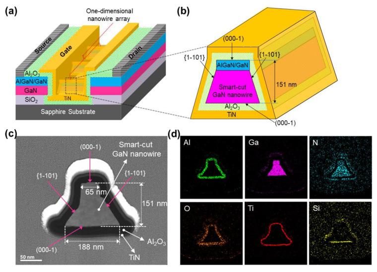
Figure 1a (on the left side) illustrates the schematic architecture of the investigated AlGaN/GaN nanowire WGT device. It has a 2-μm gate length consisting of 64 trapezoidal shaped one-dimensional nanowires, each having two similar {1–101} crystal facets (Figure 1b). On the left side of Figure 1c, an FE-TEM image clearly shows a trapezoidal-shaped AlGaN/GaN nanowire core surrounded by gate–oxide (Al2O3) and gate–metal (TiN). Figure 1d shows the spatial elemental mapping distributions of Al, Ga, N, O, Ti, and Si in the fabricated device architecture, which are examined using STEM consists with energy-dispersive X-ray (EDX) arrangement to verify the self-limited growth of the AlGaN/GaN nanowire WG architecture.
Figure 1.
(a) Graphical device design of the fabricated AlGaN/GaN nanowire WGT. (b) Cross-section image of a trapezoidal-shaped AlGaN/GaN nanowire. (c) High-resolution FE-TEM image of the AlGaN/GaN nanowire WG structure. (d) Elemental spatial mapping of Al (green), Ga (pink), N (cyan), O (orange), Ti (red), and Si (yellow) in the device design scanned using STEM-EDX.
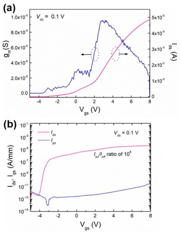
Figure 2a shows that the transistor exhibits normal operation with a threshold voltage (Vth) of ∼−1.5V. The obtained threshold voltage may be due to the full depletion of the lateral trapezoidal-shaped cross-section of the narrow channel. The maximum drain current (Id,max) of nearly ∼0.05 mA and maximum transconductance (gm) peak of nearly ∼0.01 mS at Vgs = 8 V and Vds = 0.1 V are exhibited. Furthermore, the semi-logarithmic transfer characteristics are shown in Figure 2b. The device leakage current is as low as ∼10−11 A∙mm−1. The device exhibits a high Ion/Ioff ratio of 108.
Figure 2.
(a) Transconductance (gm) and linear scales of the drain current (Ids) as a function of gate-source voltage (Vgs). (b) Logarithmic scales of drain current (Ids) as well as the gate current of (Igs) according to the Vgs of the measured AlGaN/GaN nanowire WGT at Vds = 0.1 V.
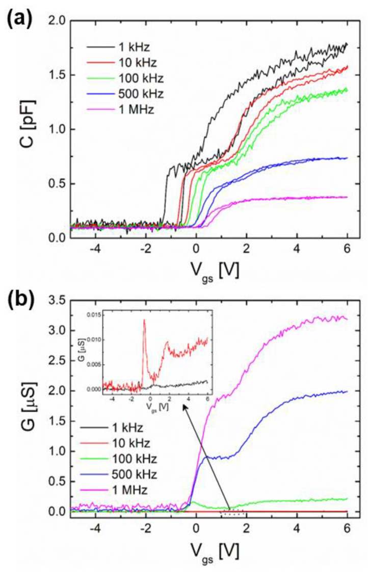
Figure 3a shows the C–V measurements of AlGaN/GaN nanowire WGT measured from low frequency (1 kHz) to high frequency (1 MHz). The measured C–V curve exhibits four different bias regions, such as barrier accumulation, 2DEG accumulation, surface depletion, and total depletion of the whole nanowire channel. Generally, the surface inversion is missing because of the significantly long-lasting minority carrier generation that occurs in GaN-based materials [18,19]. It is observed that the barrier accumulation happens at an immense positive bias shift of the flat-band voltage (VFB), with drastic frequency distribution as frequency rises. In addition, the change in flat-band voltage (ΔVFB) shift in hysteresis curves drops with rising frequency, and values are shown in Table 1. The observed strong frequency dispersion on C–V curves at the accumulation is mainly due to the trapping of electrons at border traps in the Al2O3 insulator. Such phenomena, i.e., overestimation of the oxide capacitance at the accumulation due to a decrease in frequency, were previously observed in many oxide/III-V semiconductor devices [20]. In addition, this extreme frequency dispersion is caused by a large number of surface-related traps with different lifetimes. The associated interface trap capacitance (Cit) is substantial, and the surface traps respond well to low/intermediate-level alternating-current (AC) wave frequencies, but not well to high frequencies [18,21]. The dispersion may also be caused by the deep traps that were additionally injected into the GaN film at the time of the wafer bonding method. High frequency causes a serious scattering in the barrier accumulation layer and a high positive bias shift of VFB with enlarging frequency because the trapped carriers are unable to react to the AC wave and are, therefore, unable to allow the current motion.
Figure 3.
(a) C versus Vgs and (b) G versus Vgs as functions of frequency of the AlGaN/GaN nanowire WGT.
Table 1.
Calculated experimental parameters obtained from capacitance and frequency measurements.
| Frequency, f (kHz) | VFB (V) | ΔVFB (V) | Dit (eV−1∙cm−2) |
|---|---|---|---|
| 1 | −1.21 | 0.72 | 9.1 × 10¹³ |
| 10 | −0.60 | 0.33 | 8.5 × 10¹² |
| 100 | −0.16 | 0.28 | 1.7 × 10¹² |
| 500 | 0.17 | 0.24 | 7.1 × 10¹¹ |
| 1000 | 0.28 | 0.21 | 1.2 × 10¹¹ |
Figure 3b presents the G–V characteristics for the measured nanowire device. The G–V curve decreases to negative bias, but rises with enhancing frequency, oppositely to the C–V characteristics. Additionally, it is noted that the G–V peak exists at a lower frequency range (~1 to 100 kHz) but vanishes at a higher frequency range (~500 to 1000 kHz). The surface traps with variable time responses, as mentioned in C–V characteristics, are the exact same source from which the conductance behavior derives. This states that at low frequencies, the surface traps perhaps obey the frequency and then contribute obviously to the fabricated device conductance (the period of frequency is larger than the lifetime of trapped carriers) [18,22,23]. The trapped carriers almost cannot obey the AC wave at adequately high frequencies (>500 kHz), opposite to lower frequency ranges, and do not devote to the consistent conductance. Particularly, in contrast to low frequencies, the time constant at high frequencies is substantially bigger than the period, making it impossible for the charges at traps to obey the AC wave.
The interface state density (Dit) is calculated using the Hill–Coleman phenomena [24], such that
| (1) |
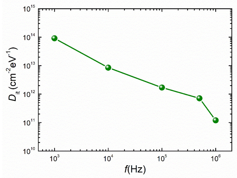
where q is the electron charge, and A is the area of contact. COX is the oxide capacitance, which can be evaluated from capacitance and conductance characteristics in strong accumulation regions at high-frequency regimes. Dit is evaluated using Equation (1) and values of 9.1 × 10¹³ (at 1 kHz), 8.5 × 10¹² (at 10 kHz), 1.7 × 10¹² (at 100 kHz), 7.1 × 10¹¹ (at 500 kHz), and 1.2 × 10¹¹ eV−1∙cm−2 (at 1 MHz) were obtained, respectively. In a similar range of values found from oxide-based III–V semiconductor interfaces [18,19,20], the obtained Dit values drop with increasing frequency, as shown in Figure 4. More precisely, if the frequency decreases, more traps are located at a deeper response. The strong dispersion influences on the C–V and G–V properties are caused by the high value of Dit.
Figure 4.
The effective Dit versus frequency for the AlGaN/GaN nanowire WGT.
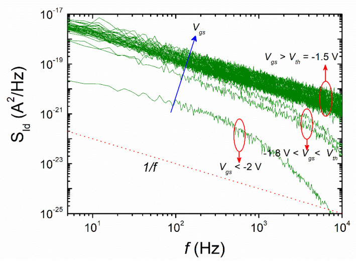
To further clearly investigate the trapping effect through the noise measurements, low-frequency noise tests are carried out to more thoroughly examine the trapping effect in the one-dimensional AlGaN/GaN nanowire WGT. It is widely known that 1/f-noise plots can provide precise information on the nature of the carrier conduction at the surface/bulk of the materials when combined with other electrical measurements. To investigate impurities and defects with deep-level traps in bulk materials and to assess the suitability (i.e., for microwave communication systems), standard quality, and reliability of semiconductor-based devices, low-frequency noise characteristics are employed [25,26]. When the gate bias is changed from the deep subthreshold to a strong accumulation regime, the power spectral density (PSD, SId) of the current/voltage dispersions is measured at Vds = 0.1 V and a frequency range of 4–104 Hz. As seen in Figure 5, the PSD elevates to the gate voltage. The noise plots distinctly display a 1/f-plot shape in the strong accumulation region (Vgs > Vth = −1.5 V), indicating that the noise is primarily caused by electron movements between the surface states with shallow levels and the accumulated surface channel layer, as mentioned before in the capacitance and conductance measurements. In the depletion region (−1.8 V < Vgs < Vth), the device exhibits 1/f-noise behavior, while beyond 1 kHz, it exhibits 1/f2-noise characteristics (i.e., Lorentzian-like (1/fγ, γ = 2)). The G–R noise that results from carrier transfer processes via trap/detrap between the 2DEG channel and traps in the GaN film with approximately shorter time constants is believed to be the cause of these 1/f2 characteristics [27,28]. This indicates that the carriers know how trapping and detrapping alike are at the interface and in the surface depletion layer of the channel. At Vgs < −2 V (i.e., deep-subthreshold regime), the cutoff frequency for the 1/f2-noise curve moves to a lower frequency (∼102 Hz) edge. This behavior is due to the G–R-based carrier transfer mechanism with comparably longer lifetime constants.
Figure 5.
Typical power spectral distribution (PSD) of low-frequency noise for the measured AlGaN/GaN nanowire WGT (at Vds = 0.1 V).
4. Conclusions
In summary, with the help of frequency-dependent capacitance–voltage (C–V) and conductance–voltage (G–V) measurements, the trapping effects and low-frequency noise measurements of trapezoidal-shaped lateral one-dimensional AlGaN/GaN nanowire WGTs fabricated using the top-down method are examined. The device displays electrical characteristics such as a high Ion/Ioff ratio of around 108. It has been shown that the device’s capacitance, conductance, and noise properties are significantly influenced by the high trap density present both at the nanowire channel’s surface and in its core. According to the 1/f-noise plots, the power spectral density displays 1/f-noise behavior in the accumulation regime and rises with gate bias. The device displays 1/f-noise behavior at low-frequency range and 1/f2-noise behavior at 1 kHz. The cutoff frequency for the 1/f2-noise plots also shifts to the lower frequency (102 Hz) side when the nanodevice rules in the deep-subthreshold regime. Our findings are expected to be exploited for the evolution of high-performance one-dimensional AlGaN/GaN nanowire WGTs.
Acknowledgments
The authors sincerely thank Jung-Hee Lee and Sorin Cristoleveanu.
Author Contributions
Conceptualization, S.P.R.M. and K.-S.I.; methodology, S.P.R.M. and K.-S.I.; validation, S.P.R.M. and P.P.; formal analysis, S.P.R.M., P.P., D.-Y.L., Y.K., H.-J.K. and S.-J.A.; investigation, S.P.R.M., P.P. and K.-S.I.; resources, S.P.R.M., K.-S.I. and S.-J.A.; writing—original draft preparation, S.P.R.M. and P.P.; writing—review and editing, S.P.R.M., P.P., K.-S.I. and S.-J.A.; visualization, S.P.R.M. and P.P.; supervision, K.-S.I. and S.-J.A. All authors have read and agreed to the published version of the manuscript.
Data Availability Statement
The data are available on reasonable request from the corresponding author.
Conflicts of Interest
The authors declare no conflict of interest.
Funding Statement
This research was supported by the Basic Science Research Program through the National Research Foundation of Korea (NRF), funded by the Ministry of Education (NRF-2022R1I1A1A01064248). It was partially supported by NRF-2018R1A6A1A03025761 and the Korea Innovation Foundation (INNOPOLIS) grant funded by the Korean government (MSIT) (2020-DD-UP-0278). Also supported by NRF-2022R1A2C1003596 and NRF-2018R1D1A1B07050766.
Footnotes
Disclaimer/Publisher’s Note: The statements, opinions and data contained in all publications are solely those of the individual author(s) and contributor(s) and not of MDPI and/or the editor(s). MDPI and/or the editor(s) disclaim responsibility for any injury to people or property resulting from any ideas, methods, instructions or products referred to in the content.
References
- 1.Lieber C.M., Wang Z.L. Functional nanowires. MRS Bull. 2007;32:99–108. doi: 10.1557/mrs2007.41. [DOI] [Google Scholar]
- 2.Calarco R., Stoica T., Brandt O., Geelhaar L. Surface-induced effects in GaN nanowires. J. Mater. Res. 2007;26:2157–2168. doi: 10.1557/jmr.2011.211. [DOI] [Google Scholar]
- 3.Yang P., Yan R., Fardy M. Semiconductor nanowire: What’s next? Nano. Lett. 2010;10:1529–1536. doi: 10.1021/nl100665r. [DOI] [PubMed] [Google Scholar]
- 4.He T., Zhang X., Ding X., Sun C., Zhao Y., Yu Q., Ning J., Wang R., Yu G., Lu S., et al. Broadband Ultraviolet Photodetector Based on Vertical Ga2O3/GaN Nanowire Array with High Responsivity. Adv. Opt. Mater. 2019;7:1801563. doi: 10.1002/adom.201801563. [DOI] [Google Scholar]
- 5.Kumar N., Raman A. Prospective sensing applications of novel heteromaterial based dopingless nanowire-TFET at low operating voltage. IEEE Trans. Nanotechnol. 2020;19:527–534. doi: 10.1109/TNANO.2020.3005026. [DOI] [Google Scholar]
- 6.Ranjan R., Kashyap N., Raman A. High-performance dual-gate-charge-plasma-AlGaN/GaN MIS-HEMT. Appl. Phys. A. 2020;126:169. doi: 10.1007/s00339-020-3342-x. [DOI] [Google Scholar]
- 7.Raman A., Chattopadhayay S.P., Ranjan R., Kakkar D., Sharma R. Design and investigation of dual dielectric recessed-gate AlGaN/GaN HEMT as gas sensor application. Trans. Electr. Electron. Mater. 2022;23:618–623. doi: 10.1007/s42341-022-00391-y. [DOI] [Google Scholar]
- 8.Im K.-S. Impact of fin width on low-frequency noise in AlGaN/GaN finFETs: Evidence for bulk conduction. IEEE Access. 2023;11:10384. doi: 10.1109/ACCESS.2023.3240409. [DOI] [Google Scholar]
- 9.Mallem S.P.R., Puneetha P., Choi Y., Baek S.M., An J.A., Im K.-S. Temperature-dependent carrier transport in GaN nanowire wrap-gate transistor. Nanomaterials. 2023;13:1629. doi: 10.3390/nano13101629. [DOI] [PMC free article] [PubMed] [Google Scholar]
- 10.Im K.-S., Sindhuri V., Jo Y.-W., Son D.-H., Lee J.-H., Cristoloveanu S. Fabrication of AlGaN/GaN Ω-shaped nanowire fin-shaped FETs by a top-down approach. Appl. Phys. Express. 2015;8:066501. doi: 10.7567/APEX.8.066501. [DOI] [Google Scholar]
- 11.Im K.-S., Reddy M.S.P., Caulmione R., Theodorou C.G., Ghibaudo G., Cristoloveanu S., Lee J.-H. Low-frequency noise characteristics of GaN nanowire gate-all-around transistors with/without 2-DEG channel. IEEE Trans. Electron Devices. 2019;66:1243–1248. doi: 10.1109/TED.2019.2894806. [DOI] [Google Scholar]
- 12.Chen H.M., Chen Y.F., Lee M.C., Feng M.S. Persistent photoconductivity in n-type GaN. J. Appl. Phys. 1997;82:899–901. doi: 10.1063/1.365859. [DOI] [Google Scholar]
- 13.Reddy C.V., Balakrishna K., Okumura H., Yoshida S. The origin of persistent photoconductivity and its relationship with yellow luminescence in molecular beam epitaxy grown undoped GaN. Appl. Phys. Lett. 1998;73:244. doi: 10.1063/1.121769. [DOI] [Google Scholar]
- 14.Hirsch M.T., Wolk J.A., Walukiewicz W., Haller E.E. Persistent photoconductivity in n-type GaN. Appl. Phys. Lett. 1997;71:1098–1100. doi: 10.1063/1.119738. [DOI] [Google Scholar]
- 15.Polenta L., Rossi M., Cavallini A., Calarco R., Marso M., Meijers R., Richter T., Stoica T., Lüth H. Investigation on localized states in GaN nanowires. ACS Nano. 2008;2:287–292. doi: 10.1021/nn700386w. [DOI] [PubMed] [Google Scholar]
- 16.Reddy V.R., Reddy M.S., Rao P.K. Effect of rapid thermal annealing on deep level defects in the Si-doped GaN. Microelectron. Eng. 2010;87:117–121. doi: 10.1016/j.mee.2009.06.005. [DOI] [Google Scholar]
- 17.Huang H.Y., Chuang C.H., Shu C.K., Pan Y.C., Lee W.H., Chen W.K., Lee M.C. Photoluminescence and photoluminescence excitation studies of as-grown and P-implanted GaN: On the nature of yellow luminescence. Appl. Phys. Lett. 2002;80:3349–3351. doi: 10.1063/1.1476400. [DOI] [Google Scholar]
- 18.Reddy M.S.P., Im K.-S., Lee J.-H., Caulmione R., Cristoloveanu S. Trap and 1/f-noise effects at the surface and core of GaN nanowire gate-all-around FET structure. Nano Res. 2019;12:809–814. doi: 10.1007/s12274-019-2292-0. [DOI] [Google Scholar]
- 19.Kang H.S., Siva Pratap Reddy M., Kim D.S., Kim K.W., Ha J.B., Lee Y.S., Choi H.C., Lee J.H. Effect of oxygen species on the positive flatband voltage shift in Al2O3/GaN metal-insulator-semiconductor capacitors with post-deposition annealing. J. Phys. D Appl. Phys. 2013;46:155101. doi: 10.1088/0022-3727/46/15/155101. [DOI] [Google Scholar]
- 20.Matys M., Adamowich B., Domanowska A., Michalewicz A., Stoklas R., Akazawa M., Yatabe Z., Hashizume T. On the origigin of interface states at oxide/III-nitride heterjunction interfaces. J. Appl. Phys. 2016;120:225305. doi: 10.1063/1.4971409. [DOI] [Google Scholar]
- 21.Bülbül M.M., Zeyrek S. Frequency dependent capacitance and conductancevoltage characteristics of Al/Si3N4/p-Si(100) MIS diodes. Microelectron. Eng. 2006;83:2522–2526. doi: 10.1016/j.mee.2006.06.002. [DOI] [Google Scholar]
- 22.Güçlü Ç.Ş., Özdemir A.F., Kökce A., Altindal Ş. Frequency and voltagedependent dielectric properties and AC electrical conductivity of (Au/Ti)/Al2O3/n-GaAs with thin Al2O3 interfacial layer at room temperature. Acta Phys. Pol. A. 2016;130:325–330. doi: 10.12693/APhysPolA.130.325. [DOI] [Google Scholar]
- 23.Nicollian E.H., Brews J.R. MOS (Metal-Oxide-Semiconductor) Physics and Technology. John Wiley & Sons; New York, NY, USA: 1982. [Google Scholar]
- 24.Hill W.A., Coleman C.C. A single-frequency approximation for interfacestate density determination. Solid State Electron. 1980;23:987–993. doi: 10.1016/0038-1101(80)90064-7. [DOI] [Google Scholar]
- 25.Balandin A., Cai S., Li R., Wang K.L., Rao V.R., Viswanathan C.R. Flicker noise in GaN/Al0.15Ga0.85N doped channel heterostructure field effect transistors. IEEE Electron Device Lett. 1998;19:475–477. doi: 10.1109/55.735751. [DOI] [Google Scholar]
- 26.Levinshtein M.E., Rumyantsev S.L., Gaska R., Yang J.W., Shur M.S. AlGaN/GaN high electron mobility field effect transistors with low 1/f noise. Appl. Phys. Lett. 1998;73:1089–1091. doi: 10.1063/1.122093. [DOI] [Google Scholar]
- 27.Vodapply S., Theodorou C.G., Bae Y., Ghibaudo G., Cristoloveanu S., Im K.-S., Lee J.-H. Comparison for 1/f noise characteristics of AlGaN/GaN FinFET and planar MISHFET. IEEE Trans. Electron Devices. 2017;64:3634–3638. doi: 10.1109/TED.2017.2730919. [DOI] [Google Scholar]
- 28.Reddy M.S.P., Park W.-S., Im K.-I., Lee J.-H. Dual-surface modification of AlGaN/GaN HEMTs using TMAH and piranha solutions for enhancing current and 1/f-noise characteristics. IEEE J. Electron Devices Soc. 2018;6:791–796. doi: 10.1109/JEDS.2018.2849444. [DOI] [Google Scholar]
Associated Data
This section collects any data citations, data availability statements, or supplementary materials included in this article.
Data Availability Statement
The data are available on reasonable request from the corresponding author.


