Abstract
Neuromorphic computing, reconfigurable optical metamaterials that are operational over a wide spectral range, holographic and nonvolatile displays of extremely high resolution, integrated smart photonics, and many other applications need next-generation phase-change materials (PCMs) with better energy efficiency and wider temperature and spectral ranges to increase reliability compared to current flagship PCMs, such as Ge2Sb2Te5 or doped Sb2Te. Gallium tellurides are favorable compounds to achieve the necessary requirements because of their higher melting and crystallization temperatures, combined with low switching power and fast switching rate. Ga2Te3 and non-stoichiometric alloys appear to be atypical PCMs; they are characterized by regular tetrahedral structures and the absence of metavalent bonding. The sp3 gallium hybridization in cubic and amorphous Ga2Te3 is also different from conventional p-bonding in flagship PCMs, raising questions about its phase-change mechanism. Furthermore, gallium tellurides exhibit a number of unexpected and highly unusual phenomena, such as nanotectonic compression and viscosity anomalies just above their melting points. Using high-energy X-ray diffraction, supported by first-principles simulations, we will elucidate the atomic structure of amorphous Ga2Te5 PLD films, compare it with the crystal structure of tetragonal gallium pentatelluride, and investigate the electrical, optical, and thermal properties of these two materials to assess their potential for memory applications, among others.
Keywords: phase-change materials, synchrotron diffraction, first-principles molecular dynamics
1. Introduction
Brain-inspired computing [1,2,3], light-controlled (i.e., over a wide spectral range, from visible to THz) or electrically controlled reconfigurable optical metamaterials [4,5,6], high resolution holographic and nonvolatile displays [7,8], integrated photonic circuits [9,10], and many other applications need next-generation phase-change materials (PCMs) with better energy efficiency and wider temperature and spectral ranges to increase reliability compared to current flagship PCMs, such as Ge2Sb2Te5, doped Sb2Te, etc. Gallium tellurides seem to be promising candidates to achieve the necessary requirements because of their higher melting and crystallization temperatures, combined with low switching power and fast switching rate [11,12,13]. Ga2Te3 and non-stoichiometric compositions appear to be atypical PCMs; they are characterized by regular tetrahedral structures, the absence of Peierls distortion in the crystalline phase, and metavalent bonding [14,15,16]. The sp3 gallium hybridization in cubic and amorphous Ga2Te3 [16,17] is also different from conventional p-bonding in flagship PCMs, raising questions about its phase-change mechanism. In addition, gallium tellurides exhibit a number of unexpected and highly unusual phenomena, such as nanotectonic compression [15] and viscosity anomalies just above their melting points [18,19]. Nanotectonic compression involves the simultaneous co-crystallization of the stable ambient and metastable high pressure (HP) forms via heating of glassy g-GaTe3 to above the glass transition temperature . The appearance of metallic HP-polymorphs seems to be beneficial for PCM performance because of the resulting higher optical and electric contrast, accompanied by lower power consumption and the possibility of multilevel writing [16]. The viscosity anomaly for several Ga-Te melts in the vicinity of a sesquitelluride composition [18,19] appears to be more significant than the observed “double kink” in liquid germanium tellurides and other PCM alloys [20,21,22,23], allowing us to distinguish between two contrasting models: (1) fragile-to-strong transition [20,21,22] and (2) incipient liquid–liquid immiscibility [23]. Recent high-energy X-ray [24] and neutron diffraction measurements have shown enhanced small-angle scattering below the scattering vector ≲ 0.4 Å−1; this is related to the dense metallic liquid droplets in the semiconducting Ga2Te3 melt and correlates with non-monotonic viscosity behavior, which can be quantitatively described by the Taylor model [25] for two-phase emulsions. The incipient transient immiscibility within a semiconductor–metal transition in liquid telluride PCMs is an interesting topic for further studies.
The main objectives of the current report are to unravel the atomic structure of amorphous Ga2Te5 pulsed laser deposition (PLD) film using high-energy X-ray diffraction, supported by first-principles simulations, and to compare it with the crystal structure of tetragonal gallium pentatelluride [26,27]. The PLD technique is often used for PCM growth, as it provides a stoichiometric transfer from the target to the deposited film and achieves a higher deposition rate [28,29]. In contrast to cubic gallium sesquitelluride Ga2Te3, which is a congruently melting compound in the Ga-Te binary system [30,31,32], tetragonal Ga2Te5 is stable over a limited temperature range and exhibits peritectic decomposition before melting. Consequently, the relationship between the amorphous material—obtained by the near instantaneous freezing of the highly excited fragments, particles, liquid globules, etc., existing in the laser-induced plasma (plume)—and a metastable crystal is expected to be complex, leaving room for various intermediate configurations and states. Deep insights into the atomic structure and associated electronic, optical, thermal, and other properties are a key for the rational design of next-generation PCMs and new functional materials for use in photovoltaic, thermoelectric, DNA sensing, and energy storage applications [33,34,35,36,37].
2. Materials and Methods
2.1. Glass and Target Synthesis, Pulsed Laser Deposition
Two different synthesis strategies were applied in efforts to synthesize glassy g-Ga2Te5 alloys. First, a small sample (300 mg) of high-purity gallium (99.999%, Neyco) and tellurium (99.999%, Cerac) was prepared in a thin-walled silica tube, which was then sealed under vacuum (10−4 mbar) and placed in a rocking furnace. The maximum temperature was 1250 K. The synthesized and homogenized sample was rapidly quenched using a salty ice/water mixture. The crystalline sample was synthesized using fast quenching. Second, a two-step synthesis technique was applied for splat quenching. Crystalline Ga2Te5 was prepared as the intermediate step via a conventional melt quenching technique. A tiny piece of the synthesized material was placed into a silica capillary, heated to ≈1050 K, and kept at this temperature for one hour, with subsequent cooling to 950 K. After a supplementary equilibration step for 30 min, the sample was splat-quenched under an argon atmosphere onto a fused silica plate cooled to ≈80 K. A mostly vitreous sample was obtained via splat-quenching.
The gallium pentatelluride target, Ga2Te5, for pulsed laser deposition was synthesized in a flat-bottom silica tube with a 25 mm inner diameter. The detailed procedure was described earlier [16], resulting in the final monolithic target with a thickness of 7 mm.
Ga2Te5 thin films were deposited at room temperature via PLD onto LCD-grade float glass substrates (Kintec Company, Hong Kong) with a substrate diameter of 2” and a thickness of 1.1 mm. A Neocera PLD system equipped with a 248 nm KrF excimer laser (Coherent Compex 102 F) was used for thin film deposition. The laser beam was focused on a ≈5 mm2 spot on the surface of the rotating target. The target-to-substrate distance was set at 9 cm, and the pressure in the vacuum chamber was around 3 × 10⁻⁶ mbar with no background gas pressure. For the preparation of “thick” layers with a thickness of ≈2 μm, 140,000 laser pulses of 200 mJ pulse energy and 10 Hz repetition rate were used. On the other hand, the “thin” layers with a thickness of ≈100 nm were prepared using 7000 laser pulses of 200 mJ pulse energy and 10 Hz repetition rate. A detailed PLD procedure was reported previously [16,38]. The chemical composition of the PLD films was verified via energy dispersive X-ray spectroscopy and found to be consistent with the target composition: 29.3 ± 0.6 at.% Ga and 70.7 ± 2.0 at.% Te.
2.2. XRD and DSC Characterization
In situ XRD measurements of a Ga2Te5 PLD film as a function of temperature have been carried out using a Rigaku Ultima IV diffractometer equipped with a Rigaku SHT-1500 high-temperature platinum camera and sealed Co Kα X-ray tube. The sample was cut from the PLD film on the glass substrate and had dimensions of 9 × 18 mm. The heating rate was 10 K min−1 in nitrogen atmosphere. The temperature range was 443 to 653 K with a step of 10 K. After temperature measurements and cooling down the sample, the diffraction pattern was recorded again under ambient conditions. Room-temperature XRD experiments have also been carried out using a Bruker D8 Advance diffractometer (the Cu Kα incident radiation) equipped with a LinxEye detector.
A PLD film powder, removed from the substrate, was used for DSC measurements employing a high precision Netzsch DSC 204 F1 Phoenix instrument (Germany) with μ-sensor. A standard aluminum pan was used for the experiments with a typical heating rate of 10 K min−1.
2.3. Optical and Electrical Measurements
Optical absorption measurements have been carried out over a wide spectral region from 700 nm to 6 μm. A Shimadzu UV-3600 spectrophotometer was used for experiments in the wavelength range of 700–3200 nm. To cover the far-IR region, a Bruker Tensor FTIR spectrometer was used with the extended IR range up to 25 μm. However, the range was limited by 6 μm due to phonon absorption in the glass substrate. The two instruments had overlapping spectral domains in the range of 2.5 and 3.2 μm.
The electrical conductivity of the samples was measured employing a Hewlett Packard 4194A impedance meter over a frequency range of 100 Hz to 15 MHz. The sample resistance was determined by analyzing the complex impedance plots and was then converted into electrical conductivity using the geometrical factor. Further experimental details can be found elsewhere [15].
2.4. High-Energy X-ray Diffraction Measurements
The 6-ID-D beamline at the Advanced Photon Source (Argonne National Laboratory, Chicago, IL, USA) was used for high-energy X-ray diffraction measurements in the top-up mode. The photon energy was 99.9593 keV, and the wavelength was 0.124035 Å. A two-dimensional (2D) setup was used for data collection with a Varex area detector, 2880 × 2880 pixels, and a pixel size of 150 × 150 μm2. The sample-to-detector distance was 302.5 mm. A Ga2Te5 PLD film powder, removed from the substrate, was placed into a silica capillary, which was fixed using a sample holder of the instrument. Cerium dioxide CeO2 was used as a calibrant. The 2D diffraction patterns were reduced using the Fit2D software [39]. The measured background intensity of the empty capillary was subtracted, and corrections were made for the different detector geometries and efficiencies, sample self-attenuation, and Compton scattering applying standard procedures [40], providing the X-ray structure factor :
| (1) |
where represents -dependent X-ray weighting coefficients and represents the Faber–Ziman partial structure factors.
2.5. First-Principles Simulation Details
The Born–Oppenheimer molecular dynamics implemented within the CP2K package [41] was used for the modeling of the diffraction data. The generalized gradient approximation (GGA) and the PBE0 hybrid exchange–correlation functional [42,43] combining the exact Hartree–Fock and DFT approaches were used, providing better agreement with experiments [15,16,38,44,45,46]. The van der Waals dispersion corrections [47] were also employed, improving first-principles molecular dynamics (FPMD) results for telluride systems [48,49]. The applied FPMD technique was similar to previous reports [44,45,46]. The initial atomic configurations for amorphous Ga2Te5 were created and optimized using the RMC_POT++ code [50] in comparison with the experimental . The cubic simulation box, containing 210 atoms (60 Ga and 150 Te), has a size matching the experimental density. Further optimization was carried out using DFT, applying the molecularly optimized correlation consistent polarized triple-zeta valence basis set along with the norm-conserving relativistic Goedecker–Teter–Hutter-type pseudopotentials [51]. FPMD simulations were performed using a canonical NVT ensemble employing a Nosé–Hoover thermostat [52,53]. The simulation boxes were heated from 300 K to 1500 K using 100 K steps for 20–25 ps each. At the highest temperature, the systems were equilibrated for 30 ps and cooled down to 300 K using the same temperature steps but with a longer simulation time (25–30 ps). Final equilibration and data collection at 300 K were performed for 34 ps. The connectivity and ring statistics were analyzed using the R. I. N. G. S. package [54] and a modified connectivity program [55]. The pyMolDyn code [56] was used for the calculation of microscopic voids and cavities.
3. Thermal Properties and Crystallization on Heating
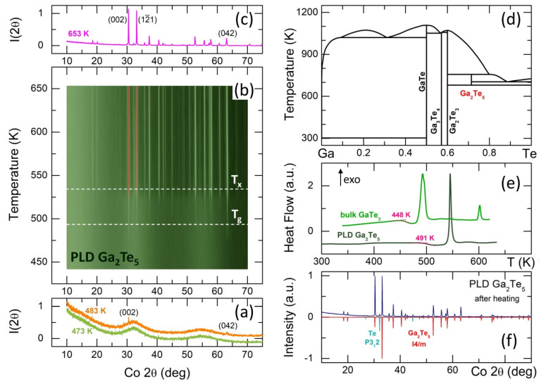
The obtained Ga2Te5 PLD thin films were found to be amorphous and vitreous according to XRD and DSC measurements. Typical DSC traces of Ga2Te5 PLD and bulk glassy g-GaTe3 are shown in Figure 1e. The endothermic glass transition temperature increases with the gallium content from 448 K (g-GaTe3, 25 at.% Ga) to 491 K (g-Ga2Te5, 28.57 at.%). This increase is accompanied by exothermic crystallization. Bulk g-GaTe3 shows two intense thermal features, peaking at 492 and 602 K, along with a very weak intermediate effect at 547 K. The 492 K peak corresponds to primary Te crystallization, presenting both the usual trigonal and high-pressure monoclinic forms. On the other hand, the 602 K feature is associated with the formation of cubic () and high-pressure rhombohedral () Ga2Te3, indicating the occurrence of nanotectonic contraction in a viscous supercooled liquid [15].
Figure 1.
Thermal properties of Ga2Te5 PLD films and crystallization on heating. In situ diffraction measurements (a) at 473 and 483 K, (b) between 443 and 653 K, (c) at 653 K; (d) Ga−Te phase diagram [30,31,32]; (e) typical DSC traces for Ga2Te5 PLD and bulk glassy g−GaTe3, and the glass transition temperatures are also indicated; (f) identification of the crystallized phases in Ga2Te5 PLD film after cooling from 653 K to room temperature. Trigonal tellurium, [57], and tetragonal Ga2Te5, [26], were found.
In contrast, g-Ga2Te5 PLD film shows a single narrow and intense exothermic effect peaking at 545 K with a crystallization onset at ≈ 535 K. The in situ XRD measurements with a typical DSC heating rate of 10 K min−1 were used to reveal the nature of crystallizing phase(s). Surprisingly, the first weak Bragg peaks at the scattering angles = 30.5° and 63.2° (the Co incident radiation) have appeared just in the vicinity of at ≈483 K, Figure 1a. They correspond to the (002) and (042) reflections of tetragonal Ga2Te5, [26], which was reported to be stable only between 673 and 768 K, Figure 1d. These unexpected results suggest the existence of certain Ga2Te5 motifs in the vitreous PLD film evolving into nano-crystallites on heating in a viscous supercooled liquid. Further crystallization advances in the vicinity of when the remaining Bragg peaks of tetragonal Ga2Te5 become visible and grow over the 513 ≲ ≲ 653 K temperature range, Figure 1b. In addition to the majority gallium pentatelluride polymorph, trigonal tellurium, [57], was also detected as a minority phase, Figure 1c,f. Even after cooling the crystallized sample, the observed phases remain intact, specifically retaining the tetragonal Ga2Te5, which is metastable at room temperature.
Even more surprisingly, gallium pentatelluride appears to be perfectly stable after 15 months at room temperature, Figure S1 (Supplementary Information), in contrast to bulk Ga2Te5, transforming into cubic Ga2Te3 and trigonal tellurium within several weeks [30]. In other words, a controlled crystallization of the amorphous Ga2Te5 PLD film yields a high-quality, stable tetragonal crystal promising for photovoltaic, thermoelectric, energy storage, and memory applications [33,34,35,36,37]. On the contrary, the slow cooling or fast quenching of molten Ga2Te5 gives a polycrystalline mixture of cubic gallium sesquitelluride and trigonal Te, Figure S1, fully consistent with the Ga-Te phase diagram, Figure 1d.
4. Electric and Optical Properties
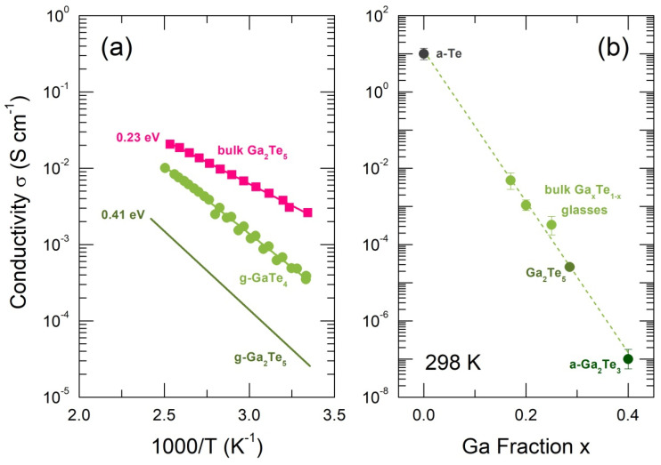
The measured electrical conductivity of bulk crystalline Ga2Te5 is shown in Figure 2a. In contrast to previously reported results [58], the electrical conductivity follows the Arrhenius relationship over the entire temperature range
| (2) |
where is the pre-exponential factor, is the conductivity activation energy, and and have their usual meanings. Nevertheless, the derived activation energy = 0.227 ± 0.003 eV is identical to that for intrinsic conductivity in tetragonal single-crystal Ga2Te5, measured in the direction perpendicular to the -axis [58]. The conductivity pre-factor, = 17 ± 3 S cm−1, was situated at the lower limit of the electronic transport regime over the extended states [59]. This indicates that = 0.45 eV is approximately the electrical bandgap.
Figure 2.
Electrical properties of amorphous, glassy, and crystalline materials: (a) electrical conductivity of bulk crystalline Ga2Te5 (this work), bulk glassy g−GaTe4 [15], and interpolated conductivity for g−Ga2Te5, and the derived activation energies are also indicated; (b) room-temperature conductivity for amorphous a−Te thin film, corresponding to band-to-band electronic transport [60], bulk Ga−Te glasses [15], and amorphous a−Ga2Te3 [61]; the interpolated value for g−Ga2Te5 is also shown.
The electrical conductivity for glassy g-Ga2Te5 was obtained via the interpolation of the available data for amorphous and glassy alloys, where 0 ≤ ≤ 0.4 [15,60,61], as shown in Figure 2b. The room-temperature conductivity appears to be a decreasing exponential function of the gallium content :
| (3) |
where is the conductivity of amorphous Te and < 0 is a constant. In other words, the electronic conductivity of disordered Ga-Te materials primarily relies on the tellurium concentration. The interpolated g-Ga2Te5 conductivity is lower by two orders of magnitude compared to the value of bulk crystalline pentatelluride. The estimated conductivity activation energy, = 0.41 eV, and the pre-exponential factor, ≈ 220 S cm−1, suggest the electrical bandgap of the glassy polymorph is about 0.8 eV.
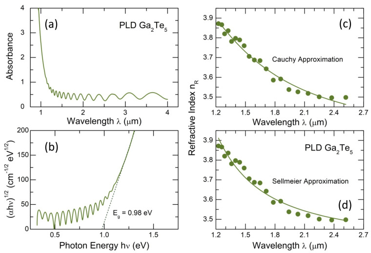
Figure 3 shows the optical properties of Ga2Te5 PLD films. The absorption measurements reveal a fundamental optical absorption edge below the incident wavelength λ ≲ 1.2 μm accompanied by distinct interference fringes. These fringes indicate a homogeneous nature and uniform thickness of the PLD film. The observed fringes allow both the refractive index and the film thickness to be calculated using the Swanepoel method [62]. Moreover, due to the well-defined interference across the spectral range and the considerable thickness of the PLD film (2.7 μm), it also becomes possible to estimate the refractive index dispersion .
Figure 3.
Optical properties of Ga2Te5 PLD films: (a) optical absorbance with interference fringes as a function of the incident wavelength ; (b) the Tauc plot, vs. photon energy , where is the absorption coefficient, yielding the optical band gap ; (c) the Cauchy and (d) Sellmeier approximations [63] describing the dispersion of the refractive index as a function of . See the text for further details.
Two approaches are usually applied to represent the refractive index dispersion [63]. The Cauchy approximation of the derived data is given in Figure 3c, as follows:
| (4) |
where , , and are constants which are characteristic of any given material. Since the Cauchy equation is inappropriate in a region of anomalous dispersion [63], the Sellmeier approach is often used, considering the existence in an optical material of dipole oscillators with a resonance frequency :
| (5) |
where and are two characteristic constants, and is the speed of light. Usually, the Sellmeier equation is written with a series of terms to account for different resonance frequencies over an extended domain, that is, , , etc.:
| (6) |
The Sellmeier coefficients and allow the normal dispersion of optical glasses to be calculated over a wide spectral range. In our case, we were limited to the original Sellmeier equation (5) with the following coefficients: = 3.5017 and = 0.3992 (Figure 3d). Due to an insufficient spectral range and experimental uncertainty, the higher-order terms in the refractive index dispersion could not be accessed. Nevertheless, despite this limitation, the two approaches describe the derived values reasonably well.
The optical absorption results were also used to calculate the optical bandgap applying the Tauc relation [64]:
| (7) |
where is the absorption coefficient, the photon energy, and ≈ 105 cm−1 eV−1 is a constant.
As expected, the derived bandgap = 0.98 ± 0.02 eV, Figure 3b, for glassy gallium pentatelluride was found to be smaller than that for g-Ga2Te3, which was 1.20 eV [16], supporting the predominant role of the tellurium content on electronic and optical properties of Ga-Te alloys. Simultaneously, the optical appears to be comparable with the electrical counterpart, = 0.82 eV.
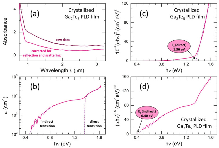
The thermally annealed and crystallized Ga2Te5 PLD film exhibits more complicated optical absorption, Figure 4. The absorbance below ≲ 1 μm shows a distinct blue-shift, while the low-energy absorbance becomes more intense and mostly loses interference fringes indicating less homogeneous material in both the chemical composition and thickness. Taking into account the presence of (nano)crystallites in the annealed PLD film, additional scattering corrections were applied simultaneously with the usual reflection corrections. The refractive index of g-Ga2Te5 was used for these calculations.
Figure 4.
Optical properties of crystallized Ga2Te5 PLD film: (a) raw absorbance data and absorbance corrected for reflection and scattering; (b) absorption coefficient α and the analysis results for direct (the dash-dotted line) and indirect (the dashed line) optical transitions; (c) data analysis suggesting direct optical transition; the derived direct optical gap is also indicated; (d) data analysis assuming indirect optical transition; the derived indirect optical gap is indicated. See the text for further details.
The Mie theory of light scattering for turbidity measurements and the wavelength exponent were employed for the scattering corrections [65,66]:
| (8) |
where is the scattering path length, and and are the intensities of the incident and transmitted beam, respectively. The turbidity depends on several parameters:
| (9) |
where is the scattering coefficient, is the particle number density, is the average volume of the particle, and is the wavelength exponent. Combining Equations (8) and (9), one obtains
| (10) |
where is the optical density and is a constant. The values of and were obtained by plotting vs. (Figure S2), which allows both the turbidity and to be determined and the scattering corrections to be calculated. The theoretical Heller wavelength exponent [65] yields the average particle size , which was found to be ≈ 110 nm for c-Ga2Te5, Figure S2. The derived value is consistent with the size of crystallites, obtained from the XRD linewidth , yielding > 50 nm. The final absorbance corrected for reflection and scattering is shown in Figure 4a.
The derived optical absorption coefficient α, presented in Figure 4b, exhibits two optical processes above and below the incident photon energy ≈ 1.3 eV. Basically, the overall shape of the absorption coefficient α is reminiscent of the behavior observed in materials such as silicon or carbon [67,68]. This shape is typically associated with direct optical transition at higher photon energies and indirect optical absorption at lower [68,69,70,71,72]. Assuming direct optical transition in crystallized Ga2Te5 above 1.3 eV,
| (11) |
the direct optical bandgap was found to be = 1.36 ± 0.03 eV, Figure 4c. The constant in Equation (11) is given by , where is the electron charge and is a reduced electron and hole effective mass [69].
The optical absorption plotted as vs. photon energy , Equation (7), yields the indirect optical bandgap = 0.40 ± 0.03 eV, Figure 4d. The derived value is consistent with the electrical bandgap of c-Ga2Te5, = 0.45 eV, Figure 2a.
The experimental data for tetragonal Ga2Te5, obtained using the conductivity and Hall effect measurements, are strongly anisotropic and changing over a wide range between 0.46 and 1.79 eV [58]. The calculated values are also variable, 0.86 ≤ ≤ 1.7 eV [72,73], depending on the applied simulation method. Nevertheless, the results of electrical and optical measurements show a reasonable contrast between amorphous (SET) and crystalline (RESET) states for Ga2Te5.
5. High-Energy X-Ray Diffraction
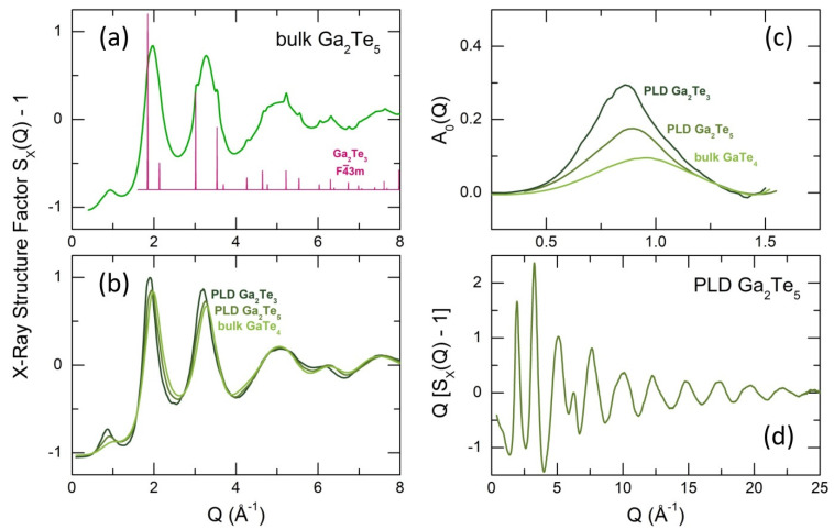
The high-energy X-ray diffraction data in -space are shown in Figure 5. In contrast to fast cooled Ga2Te5 in a thin-walled silica tube, mostly consisting of cubic Ga2Te3 and trigonal tellurium with some vitreous fraction (Figure S1), the splat-quenching of tiny Ga2Te5 droplets yields an essentially glassy material. However, this glassy material is accompanied by non-negligible nanocrystals of cubic gallium sesquisulfide, as seen in Figure 5a. The spontaneous Ga2Te3 crystallization is consistent with the Ga-Te phase diagram, Figure 1d, related to peritectic decomposition of Ga2Te5 above 768 K. The obtained Ga2Te5 PLD films are fully vitreous with a distinct glass transition temperature at 491 K, Figure 1e. The X-ray structure factor of g-Ga2Te5 PLD appears to be intermediate between bulk glassy GaTe4 and Ga2Te3 PLD film, Figure 5b, suggesting structural similarities and revealing a systematic evolution of vitreous materials with increasing gallium content independently of preparation techniques.
Figure 5.
Diffraction data in -space: the X-ray structure factor of (a) bulk splat-quenched Ga2Te5 and (b) Ga2Te3, Ga2Te5 PLD films and bulk glassy g−GaTe4 over a limited -range; (c) isolated first sharp diffraction peaks (FSDP) for Ga2Te3 and Ga2Te5 PLD films and g−GaTe4; (d) the interference function for Ga2Te5 PLD film over the extended −range. The Bragg peaks for cubic Ga2Te3 (space group ) are also shown in (a).
In particular, we observe an emerging and growing first sharp diffraction peak (FSDP), also shifting to a lower with increasing from = 0.94 ± 0.01 Å−1 (GaTe4, = 0.2) to 0.86 ± 0.01 Å−1 (Ga2Te3, = 0.4), Figure 5c. The isolated FSDPs were obtained using the subtraction procedure [74,75]. The FSDP systematics (position and amplitude ) reveals monotonic and nearly linear trends as a function of , Figure S3, for both bulk glasses (0.17 ≤ ≤ 0.25) and vitreous PLD films (0.2857 ≤ ≤ 0.40). The observed trends suggest that there are structural similarities on the short- and intermediate-range scale.
Distinct high- oscillations, clearly visible over the extended -range for the Ga2Te5 interference function , Figure 5d, enable high real-space resolution for atomic pair distribution and total correlation functions after the usual Fourier transform:
| (12) |
where is the experimental number density, the Lorch window function, and = 30 Å−1.
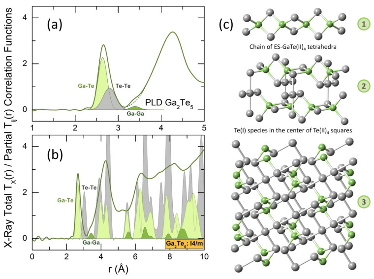
The derived for g-Ga2Te5 PLD film is shown in Figure 6. The asymmetric feature between 2.4 and 3.2 Å corresponds to Ga-Te and Te-Te nearest neighbors (NN). Gaussian fitting of the experimental data (Table 1) yields tetrahedral gallium coordination at a distance of 2.64 Å, consistent with the known Ga-Te coordination numbers and NN distances in crystalline and glassy gallium tellurides [14,15,16,26,27,30,76,77,78]. On the contrary, the Te-Te atomic pairs in glassy Ga2Te5 are markedly shorter (2.80 Å) than those in tetragonal gallium pentatelluride (3.027 Å) [26]. Nevertheless, the Te-Te NN distance of 2.80 Å is typical for amorphous and trigonal tellurium [57,79] and Te-rich binary and ternary glasses [15,77,78,80]. The partial correlation functions for tetragonal gallium pentatelluride are compared in Figure 6b with an experimental for g-Ga2Te5. We note both similarities and differences for the two materials.
Figure 6.
Diffraction data in -space: the X-ray total correlation function for g-Ga2Te5 PLD film, showing (a) a four-peak Gaussian fitting of the nearest (NN) and second (2N) neighbor features between 2.4 and 4.5 Å; the Ga-Te and Te-Te NNs are highlighted in light green and gray, respectively; the Ga-Ga 2Ns are green; (b) a comparison with the partial correlation functions for tetragonal Ga2Te5 (space group [26]), derived using the XTAL code [76]; (c) the crystal structure of tetragonal gallium pentatelluride, revealing (1) infinite chain of edge-sharing ES-GaTe(II)4 tetrahedra along the -axis, (2) two neighboring chains connected by Te(I) species located in the center of Te(II) squares, (3) an approximate () projection of the crystal structure.
Table 1.
Interatomic distances and partial coordination numbers of the nearest neighbors in glassy Ga2Te5 PLD films according to high-energy X-ray diffraction and first-principles molecular dynamics.
| Ga-Ga | Ga-Te | Te-Te | ||||
|---|---|---|---|---|---|---|
| High-energy X-ray diffraction | ||||||
| - | - | 2.637(3) | 3.98(5) | 2.796(5) | 1.01(8) | 3.98(5) |
| First-principles molecular dynamics (GGA/PBE0) | ||||||
| 2.417 | 0.03 | 2.615 * | 3.97 | 2.802 * | 0.93 | 4.00 |
* asymmetric peak.
The crystalline counterpart is stable over a narrow temperature range from 673 to 768 K [30,31,32], as shown in Figure 1d. In contrast to layered compounds like Al2Te5 and In2Te5 [27], gallium pentatelluride has a 3D structure consisting of infinite chains, parallel to the c axis. The chains are formed by edge-sharing ES-GaTe(II)4 tetrahedra, Figure 6c. Additionally, every four ES-GaTe(II)4 entities from neighboring chains are linked together by Te(I) species, located at the center of squares, formed by Te(II).
These square-planar Te5 units (crosses) are mostly absent in glassy Ga2Te5, as evidenced by the significantly lower Te-Te NN coordination number, = 1.01 ± 0.08 (Table 1), compared to the crystal counterpart, = 1.6 = ⅕ × 4 + ⅘ × 1, which represents the average Te-Te coordination for the Te(I) and Te(II) species, Figure 6c. On the other hand, the existence of ES-GaTe4 tetrahedra in the glass network is indicated by the presence of a weak shoulder at 3.39 ± 0.02 Å for the asymmetric second neighbor peak, centered at ≈4.3 Å. The short Ga-Ga second neighbor correlations, characteristic of ES-units in tetragonal Ga2Te5, are located at 3.424 Å, Figure 6b. However, due to a weak average Ga-Ga weighting factor, = 0.02964 vs. = 0.28405 or = 0.68630, the amplitude of this feature is small. The weak average Ga-Ga weighting factor, as well as the truncation ripples, related to a finite -range of the Fourier transform, enable only a rough estimation of = 1.2 ± 0.4, compared to = 2. A deep insight into the atomic structure of vitreous Ga2Te5 PLD films yields first-principles molecular dynamics.
6. First-Principles Molecular Dynamics
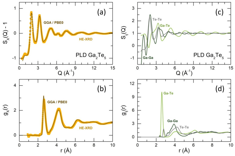
Simulated FPMD X-ray structure factor and pair-distribution function for glassy Ga2Te5 in comparison with experimental results are shown in Figure 7a,b. We note that the GGA approximation with hybrid PBE0 functional describes the experimental data well, as it was reported earlier [15,16,44,45,46]. The positions and amplitudes of the diffraction features in both - and -space are reproduced.
Figure 7.
First-principles molecular dynamics modeling of Ga2Te5 PLD film using GGA/PBE0 approximation; calculated and experimental (a) X-ray structure factors ; (b) pair-distribution functions ; (c) partial structure factors ; (d) partial pair distribution functions . The Ga−Ga, Ga−Te, and Te−Te partials are dark green, light green, and grey, respectively.
The calculated partial structure factors are displayed in Figure 7c. As expected, the main contribution to the FSDP comes from the Ga-Ga partial . The simulated , Figure 7d, reveal complicated short- and intermediate-range orders.
The asymmetric Ga-Te NN correlations appear at 2.62 Å and suggest at least two contributions with slightly different bond lengths. The Ga-Te coordination number is consistent with the experiment, = 3.97, Table 1, assuming a tetrahedral gallium local environment. In addition to homopolar Te-Te bonds at 2.80 Å, a weak Ga-Ga NN feature at 2.42 Å was also found. The amplitude of this peak is too small to be observed experimentally, Figure 7b. The Ga-Ga second neighbors between 3 and 4.5 Å have a bimodal distribution. The shoulder at ≈3.35 Å indicates the ES-units, while the main contribution at 3.92 Å is related to corner-sharing CS-entities. Consequently, the fraction of ES-GaTe4 in the glassy Ga2Te5, = 0.45, is significantly lower than that in tetragonal polymorph, = 1, indicating that only ES-GaTe4 are present in the crystalline counterpart. The experimental value, = 0.6 ± 0.2, is reasonably consistent with the FPMD result. Basically, the experimental and FPMD structural parameters were found to be similar or identical, Table 1.
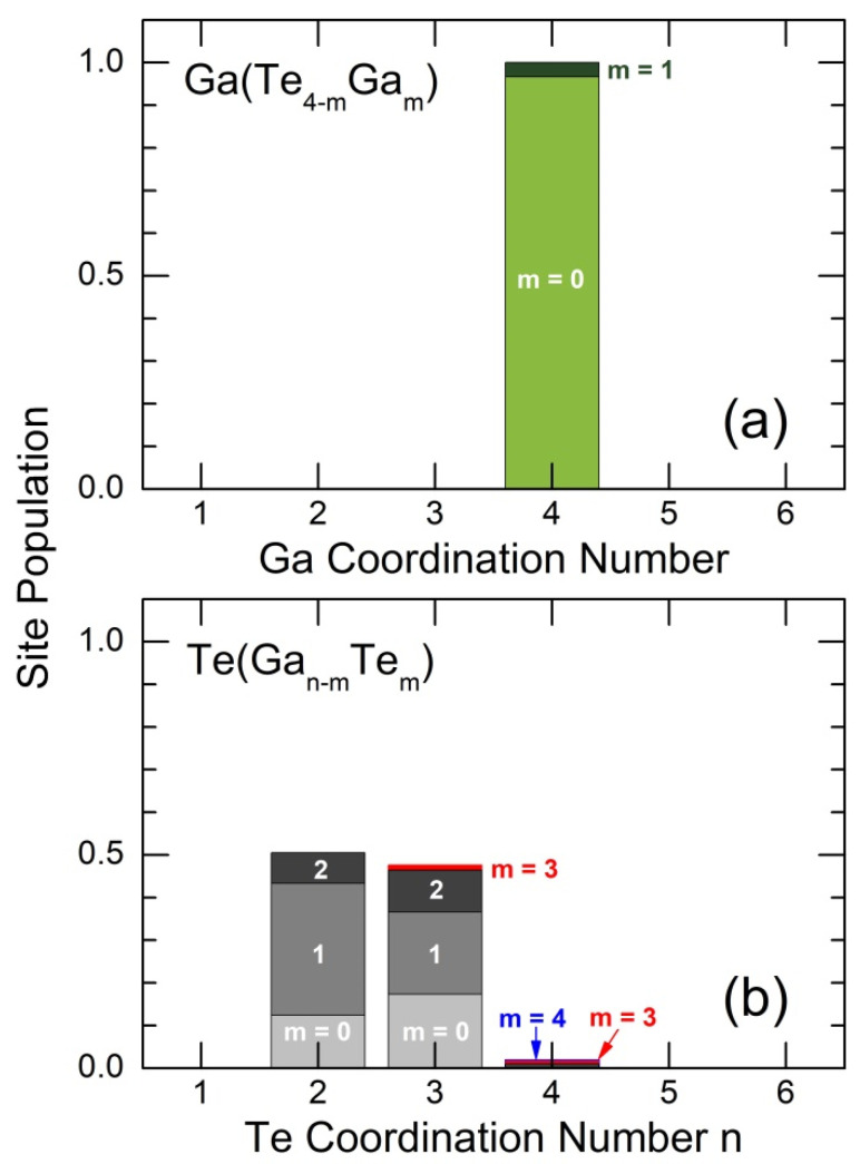
The Ga and Te local coordination distributions are presented in Figure 8. The tetrahedral gallium coordination contains negligible number of Ga-Ga homopolar pairs ( = 1). In contrast, tellurium has multiple coordination environments , 1 ≤ ≤ 4, but only two-fold Te2F (50.5%) and three-fold Te3F (47.6%) coordinated species are the most abundant. The tellurium forms reveal a large variability in Te-Te bonds, 0 ≤ ≤ 4, from pure heteropolar Te-Ga coordination ( = 0) to fully homopolar environment ( = ). We should, however, note a small fraction of Te4F species (1.87%) and a negligible number of Te5 square-planar entities (0.23%), the only form of tellurium subnetwork in tetragonal gallium pentatelluride, Figure 6c. This result is coherent with the reduced Te-Te coordination number , Table 1.
Figure 8.
(a) Gallium and (b) tellurium coordination distributions. Tetrahedral gallium coordination contains a negligible number of Ga-Ga homopolar pairs ( = 1). Multiple tellurium coordination environments , 1 ≤ ≤ 4, contain a significant number of Te−Te bonds, 0 ≤ ≤ 4. See the text for further details.
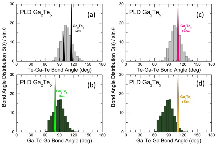
The geometry of GaTe4 units yields either Te-Ga-Te bond angles or the orientational order parameter [81,82]. Figure 9a,c show the calculated bond angle distribution for g-Ga2Te5 in comparison with tetragonal Ga2Te5 and cubic Ga2Te3, respectively. We note a broad and slightly asymmetric function, centered at 103.3 ± 0.3°, for the PLD film (Figure S4). The Te-Ga-Te angles in the two crystalline references, characterizing both distorted ES-GaTe4 tetrahedra in gallium pentatelluride and regular CS-units in cubic sesquitelluride, are located within the glassy envelope but do not reproduce it via simple broadening. Nevertheless, the tetrahedral geometry in tetragonal Ga2Te5 seems to be closer to that in the glass.
Figure 9.
Bond angle distributions in simulated g-Ga2Te5: (a,c) the Te-Ga-Te and (b,d) Ga-Te-Ga bond angles in comparison with (a,b) tetragonal Ga2Te5 and (c,d) cubic Ga2Te3.
The connectivity of GaTe4 tetrahedra is given by the Ga-Te-Ga triplets or the respective distributions, Figure 9b,d. The difference in connectivity between g-Ga2Te5 and the crystalline structures is even more significant but a remote resemblance to the connected ES-entities in the tetragonal crystal still exists.
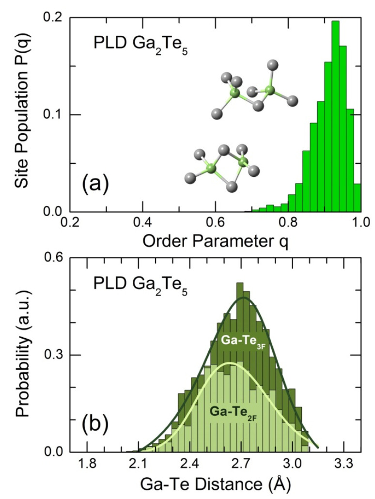
The order parameter [81,82] is often used to evaluate the polyhedral topology and distinguish between tetrahedral and non-tetrahedral local geometry of four-fold coordinated GaTe4 entities
| (13) |
where is the Te-Ga-Te angle of the central gallium atom with its nearest Te neighbors and . The average value of changes between 0 for an ideal gas and = 1 for a regular tetrahedral network. The probability distribution function is shown in Figure 10a. Asymmetric is peaked at = 0.93 and decreases sharply both ways to high and low . Usually, the tetrahedral limit is set at ≥ 0.8 [44,83]. The integration within these limitations shows that 97% of GaTe4 units belong to the tetrahedral geometry. The remaining entities (3%) are likely defect octahedral species GaTe4 with two missing Te neighbors around the central Ga atom, characterized by 0.4 < < 0.8. The regular defect octahedron ( and ) has = ⅝. The obtained results differ drastically from flagship PCM (GeTe, Ge2Sb2Te5), which show a significant fraction of defect octahedral sites and a minority of tetrahedral structural units (≲40%) [28,83,84,85,86,87]. The exact proportion varies depending on experimental technique, that is, EXAFS or diffraction, and the exchange–correlation functional for FPMD simulations.
Figure 10.
(a) Orientational order parameter [81,82] for 4-fold coordinated Ga species in g-Ga2Te5 and (b) Ga-Te NN distance distributions for two-fold Te2F and three-fold Te3F coordinated tellurium atoms.
Two-fold and three-fold coordinated tellurium can explain the asymmetric shape of the Ga-Te NN peak. The calculated Ga-Te2F and Ga-Te3F distances are presented in Figure 10b. The two distributions are broad and asymmetric but have slightly different maxima. The Ga-Te3F bonds are longer (a broad maximum at 2.71 ± 0.03 Å) compared to Ga-Te2F, peaked at 2.63 ± 0.02 Å. A similar difference, = 0.12 ± 0.01 Å, was reported in monoclinic Ga2S3 [88] with an ordered distribution of gallium vacancies. The ratio of Ga-Te3F to Ga-Te2F bond populations, = 1.75, was also found to be similar to the expected stoichiometric ratio = 2 for tetrahedral Ga species, which possess the formal oxidation state Ga3+ and correspond to the Ga2Te3 alloy composition.
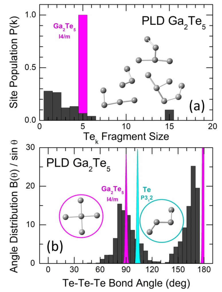
The connectivity analysis shows that all Ga and Te species are connected. The analysis of Te-Te connectivity reveals a different size of fragments, Figure 11a. Tellurium monomers ( = 1), that is, Te atoms with only heteropolar Te-Ga bonds, and dimers ( = 2) represent a relative majority, 55%, of all fragments. The remaining fragments can be divided into two groups: (i) 3 ≤ ≤ 6 (see the inset in Figure 11a) and (ii) oligomeric chains, = 15, for the used 210-atom simulation box. Group (i) represents the remnants of square-planar Te5 units in tetragonal Ga2Te5 (the inset in Figure 11b), also confirmed by bond angle distribution . Group (ii) is similar to chains in trigonal tellurium, [57], supported by a contribution at about ≈ 103°, Figure 11b. The presence of two distinct groups is likely a consequence of the limited thermal stability of tetragonal gallium pentatelluride and peritectic reaction Ga2Te5 ⇄ Ga2Te3 +2Te above 768 K.
Figure 11.
(a) Size and (b) Te-Te-Te bond angle distribution in oligomeric fragments, ≤ 15. The only population of 5-membered Te5 square-planar fragments (crosses) in tetragonal Ga2Te5 is also shown in (a), as well as the characteristic distributions in trigonal tellurium [57] and tetragonal Ga2Te5 [26]. Typical fragments in glassy and crystalline pentatellurides are shown in the insets, as well as a part of the helical tellurium chain in c-Te, [57].
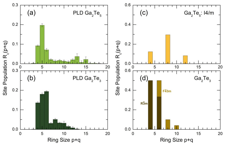
The intermediate-range order in glassy and amorphous materials is often described by ring statistics, that is, by the population of rings in the case of gallium tellurides. The ring population [54] in glassy Ga2Te5 (this work) and Ga2Te3 [16] PLD films in comparison with crystalline references (tetragonal Ga2Te5 [26], cubic [17], and rhombohedral [89] Ga2Te3) is shown in Figure 12. The population was found to be different for the two Ga2Te5 forms. The dominant eight-membered rings in tetragonal polymorphs are hardly populated in the PLD film. On the contrary, the most populated = 5 entities in g-Ga2Te5 are absent in c-Ga2Te5. The peritectic nature of tetragonal crystal seems to be related to this difference.
Figure 12.
Ring population [54] in glassy (a) Ga2Te5 (this work), (b) Ga2Te3 [16] PLD films, and crystalline references: (c) tetragonal Ga2Te5 [26], (d) cubic [17] and rhombohedral [89] Ga2Te3.
Gallium sesquitelluride Ga2Te3 is a congruently melting compound, Figure 1d. As it was reported earlier [16], the ring statistics in g-Ga2Te3 represent a disordered mixture of for the ambient and high-pressure polymorphs, Figure 12b,d, related to nanotectonic contraction in a viscous supercooled melt.
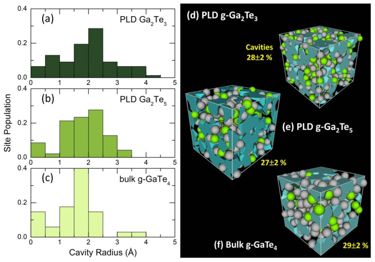
Microscopic voids and cavities in amorphous Ga-Te alloys, obtained using the Dirichlet–Voronoi tessellation [56], are displayed in Figure 13b. The fraction of voids , normalized to the volume of the FPMD simulation box, was found to be nearly invariant, 27 ≤ ≤ 29%, over the gallium content between 0.20 (bulk g-GaTe4) and 0.40 (PLD g-Ga2Te3). This is coherent with a small change in the number density, ≈2% over the same composition range. Typical cavity radius varies between 0.2 and 4 Å, slightly increasing with , Figure 13a.
Figure 13.
Microscopic voids in glassy Ga-Te alloys; typical distributions of characteristic cavity radii in (a) Ga2Te3, (b) Ga2Te5, and (c) GaTe4; snapshots of simulation boxes with microscopic voids for (d) Ga2Te3 [16], (e) Ga2Te5 (this work), and (f) GaTe4 [15], calculated using the Dirichlet–Voronoi approximation [56].
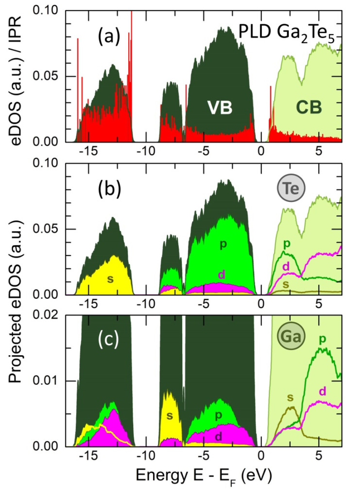
The total electronic density of states (eDOS) is shown in Figure 14 and appears to be typical for glassy and crystalline chalcogenides [15,16,59,90,91,92]. The valence band (VB) consists of three sub-bands between the Fermi level and −16 eV. The upper part, roughly centered at −3 eV, mostly consists of Te 5p and Ga 4p states and also includes non-negligible d-electron contributions, as it revealed by the eDOS projections (pDOS) on Ga and Te atomic pseudo-wave functions. The middle-energy sub-band, centered at −8 eV, essentially contains Te 5p and Ga 4s electron states, while the lower part, peaked at −13 eV, has an s-character, populated by Te 5s electrons together with Ga s-, p- and d-electron contributions. The derived eDOS and pDOS are similar to those in g-Ga2Te3 PLD film [16] and suggest sp3 gallium hybridization also has a d-electron contribution.
Figure 14.
(a) Electronic density of states (eDOS) and inverse participation ratio (IPR, red spikes) in g-Ga2Te5 PLD film at 300 K, and projected DOS on (b) tellurium and (c) gallium atomic pseudo-wave functions. The s (yellow), p (green) and (magenta) contributions are shown. VB = valence band; CB = conduction band.
The inverse participation ratio IPR [93,94] allows for localized (large IPR → 1) and extended electron states (small IPR ≈ , where is the number of atoms in the simulation box) to be distinguished
| (14) |
where is a single-particle Kohn–Sham eigenfunction. The calculated IPRs, derived using the projections of onto an atomic basis set and the atomic orbital coefficients, are shown in Figure 14a, plotted together with the eDOS. As it was reported earlier [16,46], a higher electron localization appears at the band tails (the top of the valence and the bottom of the conduction bands), consistent with the theories of disordered semiconductors [59]. The remaining electron states in the vicinity of the bandgap are delocalized (extended). Deeper states of the lower-energy sub-bands, participating in the covalent bonding, are localized even more strongly.
The derived GGA/PBE0 bandgap, = 0.80 eV, appears to be smaller than the experimental optical bandgap, = 0.98 eV, Figure 3b, but nearly identical to the interpolated electrical counterpart, = 0.82 eV, Figure 2a. The main contribution of the Te 5p electron states to the upper part of the valence band and at the bottom of the conduction band is also consistent with a dominant role played by Te on the electronic conductivity of Ga-Te alloys, Figure 2b.
7. Conclusions
Pulsed laser deposition allows for homogeneous and uniform Ga2Te5 films to be obtained, showing a distinct glass transition at 491 K and accompanied by strong crystallization peaked at 545 K. Thermal annealing of the PLD film with a DSC heating rate and carried out below the stability limits of tetragonal Ga2Te5 yields a high-quality and long-living (for at least 15 months) tetragonal polymorph that is thermodynamically metastable under ambient conditions. Amorphous and crystalline Ga2Te5 forms show reasonably high electric contrast (two orders of magnitude at room temperature) and distinctly different optical band gaps, = 0.98 eV for g-Ga2Te5 and indirect optical bandgap = 0.40 eV for c-Ga2Te5. Consequently, gallium pentatelluride can be used for memory applications as well as for photovoltaics, quantum-dots-based DNA sensors, and for the preparation of atomically thin layers via the controlled crystallization of amorphous thin films.
The local coordination of tetrahedral gallium is common for these two forms; however, the intermediate-range order and tellurium subnetwork are drastically different. Square-planar Te5 units (crosses) connecting edge-sharing Ge-Te chains in tetragonal Ga2Te5, which are formed by ES-GaTe4 tetrahedra, do not survive in the glassy polymorph, leaving remnants, 3 ≤ ≤ 6, originating from the Te5 entities and oligomeric tellurium chains similar to those in trigonal Te. Quasi-1D edge-sharing Ga-Te chains lose their exclusive structural signature, characteristic of tetragonal polymorph, transforming into 2D and 3D structural patches of edge- and corner-sharing GaTe4 tetrahedra. The simulated electronic density of states is consistent with the experimental optical and conductivity results and reveals a predominant role of the Te 5p electron states for electronic properties of gallium pentatelluride.
Supplementary Materials
The following supporting information can be downloaded at: https://www.mdpi.com/article/10.3390/nano13142137/s1, Figure S1. X-ray diffraction patterns of rapidly cooled Ga2Te5 melt and Ga2Te5 PLD film; Figure S2. Scattering corrections for crystallized Ga2Te5 PLD film; Figure S3. FSDP parameters for glassy alloys; Figure S4. Bond angle distribution in simulated g-Ga2Te5.
Author Contributions
Conceptualization, E.B. and A.T.; HE-XRD, C.J.B.; synthesis, A.T., M.B., and M.K. (Mohammad Kassem); PLD, S.B.; FPMD, RMC, and statistics, M.K. (Maxim Khomenko), A.S., and D.F.; XRD, DSC, and conductivity, A.T., M.B., and M.K. (Mohammad Kassem); optics, A.T.; paper writing, E.B. with the help of all authors. All authors have read and agreed to the published version of the manuscript.
Data Availability Statement
The data presented in this study are available on request from the corresponding author.
Conflicts of Interest
The authors declare no conflict of interest.
Funding Statement
This work was supported by the Région Hauts de France and the Ministère de l’Enseignement Supérieur et de la Recherche (CPER ECRIN), as well as by the European Fund for Regional Economic Development. Work at the Advanced Photon Source, Argonne National Laboratory, was supported in part by the Office of Basic Energy Sciences, US Department of Energy, under Contract No. DE-AC02-06CH11357. M.K. (Maxim Khomenko) works at ILIT RAS, and TSU was supported by the Ministry of Science and Higher Education under agreement 075-15-2021-917; state assignment FSRC ‘Crystallography and Photonics’ Russian Academy of Sciences; and by the Tomsk State University Development Program (Priority-2030). SB’s work was supported by the Estonian Research Council under grant number PRG1023. Partly, the measurements were carried out in the resource centers of St. Petersburg State University: “Centre for X-ray Diffraction Studies” and “Centre for Thermogravimetric and Calorimetric Research”. This work was granted access to the HPC resources of IDRIS (France) under the allocation 2022-A0130910639 made by Grand Equipement National de Calcul Intensif (GENCI) and access to the use of the CALCULCO computing platform, supported by Service COmmun du Système d’Information de l’Université du Littoral Côte d’Opale (SCoSI/ULCO). The FPMD simulations were also carried out using the HPC computing resources at Lomonosov Moscow State University and at the ILIT RAS in Shatura (Moscow Region).
Footnotes
Disclaimer/Publisher’s Note: The statements, opinions and data contained in all publications are solely those of the individual author(s) and contributor(s) and not of MDPI and/or the editor(s). MDPI and/or the editor(s) disclaim responsibility for any injury to people or property resulting from any ideas, methods, instructions or products referred to in the content.
References
- 1.Zhang W., Mazzarello R., Wuttig M., Ma E. Designing crystallization in phase-change materials for universal memory and neuro-inspired computing. Nat. Rev. Mater. 2019;4:150–168. doi: 10.1038/s41578-018-0076-x. [DOI] [Google Scholar]
- 2.Xu M., Mai X., Lin J., Zhang W., Li Y., He Y., Tong H., Hou X., Zhou P., Miao X. Recent advances on neuromorphic devices based on chalcogenide phase-change materials. Adv. Funct. Mater. 2020;30:2003419. doi: 10.1002/adfm.202003419. [DOI] [Google Scholar]
- 3.Feldmann J., Youngblood N., Karpov M., Gehring H., Li X., Stappers M., Le Gallo M., Fu X., Lukashchuk A., Raja A.S., et al. Parallel convolutional processing using an integrated photonic tensor core. Nature. 2021;589:52–61. doi: 10.1038/s41586-020-03070-1. [DOI] [PubMed] [Google Scholar]
- 4.Wang Q., Rogers E.T.F., Gholipour B., Wang C.-M., Yuan G., Teng J., Zheludev N.I. Optically reconfigurable metasurfaces and photonic devices based on phase change materials. Nat. Photon. 2016;10:60–66. doi: 10.1038/nphoton.2015.247. [DOI] [Google Scholar]
- 5.Shalaginov M.Y., An S., Zhang Y., Yang F., Su P., Liberman V., Chou J.B., Roberts C.M., Kang M., Rios C., et al. Reconfigurable all-dielectric metalens with diffraction-limited performance. Nat. Commun. 2021;12:1225. doi: 10.1038/s41467-021-21440-9. [DOI] [PMC free article] [PubMed] [Google Scholar]
- 6.Konnikova M.R., Khomenko M.D., Tverjanovich A.S., Bereznev S., Mankova A.A., Parashchuk O.D., Vasilevsky I.S., Ozheredov I.A., Shkurinov A.P., Bychkov E.A. GeTe2 phase change material for terahertz devices with reconfigurable functionalities using optical activation. ACS Appl. Mater. Interfaces. 2023;15:9638–9648. doi: 10.1021/acsami.2c21678. [DOI] [PubMed] [Google Scholar]
- 7.Dong W., Liu H., Behera J.K., Lu L., Ng R.J.H., Sreekanth K.V., Zhou X., Yang J.K.W., Simpson R.E. Wide bandgap phase change material tuned visible photonics. Adv. Funct. Mater. 2019;29:1806181. doi: 10.1002/adfm.201806181. [DOI] [Google Scholar]
- 8.Liu H., Dong W., Wang H., Lu L., Ruan Q., Tan Y.S., Simpson R.E., Yang J.K.W. Rewritable color nanoprints in antimony trisulfide films. Sci. Adv. 2020;6:eabb7171. doi: 10.1126/sciadv.abb7171. [DOI] [PMC free article] [PubMed] [Google Scholar]
- 9.Delaney M., Zeimpekis I., Lawson D., Hewak D.W., Muskens O.L. A new family of ultralow loss reversible phase-change materials for photonic integrated circuits: Sb2S3 and Sb2Se3. Adv. Funct. Mater. 2020;30:2002447. doi: 10.1002/adfm.202002447. [DOI] [Google Scholar]
- 10.Ilie S.T., Faneca J., Zeimpekis I., Domínguez Bucio T., Grabska K., Hewak D.W., Chong H.M.H., Gardes F.Y. Thermo-optic tuning of silicon nitride microring resonators with low loss non-volatile Sb2S3 phase change material. Sci. Rep. 2022;12:17815. doi: 10.1038/s41598-022-21590-w. [DOI] [PMC free article] [PubMed] [Google Scholar]
- 11.Zhu H., Yin J., Xia Y., Liu Z. Ga2Te3 phase change material for low-power phase change memory application. Appl. Phys. Lett. 2010;97:083504. doi: 10.1063/1.3483762. [DOI] [Google Scholar]
- 12.Lee D., Kim T., Sohn H. Highly reliable threshold switching behavior of amorphous Ga2Te3 films deposited by RF sputtering. Appl. Phys. Express. 2019;12:085504. doi: 10.7567/1882-0786/ab2cd9. [DOI] [Google Scholar]
- 13.Lee D., Kim T., Kim J., Sohn H. Effect of nitrogen doping on threshold voltage in amorphous Ga2Te3 for application of selector devices. Phys. Status Solidi A. 2020;217:2000478. doi: 10.1002/pssa.202000478. [DOI] [Google Scholar]
- 14.Kolobov A.V., Fons P., Krbal M., Mitrofanov K., Tominaga J., Uruga T. Local structure of the crystalline and amorphous states of Ga2Te3 phase-change alloy without resonant bonding: A combined X-ray absorption and ab initio study. Phys. Rev. B. 2017;95:054114. doi: 10.1103/PhysRevB.95.054114. [DOI] [Google Scholar]
- 15.Bokova M., Tverjanovich A., Benmore C.J., Fontanari D., Sokolov A., Khomenko M., Kassem M., Ozheredov I., Bychkov E. Unraveling the atomic structure of bulk binary Ga-Te glasses with surprising nanotectonic features for phase-change memory applications. ACS Appl. Mater. Interfaces. 2021;13:37363–37379. doi: 10.1021/acsami.1c09070. [DOI] [PubMed] [Google Scholar]
- 16.Tverjanovich A., Khomenko M., Benmore C.J., Bereznev S., Sokolov A., Fontanari D., Kiselev A., Lotin A., Bychkov E. Atypical phase-change alloy Ga2Te3: Atomic structure, incipient nanotectonic nuclei, and multilevel writing. J. Mater. Chem. C. 2021;9:17019–17032. doi: 10.1039/D1TC03850H. [DOI] [Google Scholar]
- 17.Guymont M., Tomas A., Guittard M. The structure of Ga2Te3. An X-ray and high-resolution electron microscopy study. Philos. Mag. A. 1992;66:133–139. doi: 10.1080/01418619208201518. [DOI] [Google Scholar]
- 18.Glazov V.M., Chizhevskaya S.N., Glagoleva N.N. Liquid Semiconductors. Plenum; New York, NY, USA: 1969. pp. 142–150. [Google Scholar]
- 19.Chizhevskaya S.N., Glazov V.M. A study of chemical interactions between gallium and tellurium in molten state. Zh. Neorg. Khim. 1962;7:1933–1937. [Google Scholar]
- 20.Ito K., Moynihan C.T., Angell C.A. Thermodynamic determination of fragility in liquids and a fragile-to-strong liquid transition in water. Nature. 1999;398:492–495. doi: 10.1038/19042. [DOI] [Google Scholar]
- 21.Wei S., Lucas P., Angell C.A. Phase change alloy viscosities down to Tg using Adam-Gibbs-equation fittings to excess entropy data: A fragile-to-strong transition. J. Appl. Phys. 2015;118:034903. doi: 10.1063/1.4926791. [DOI] [Google Scholar]
- 22.Orava J., Hewak D.W., Greer A.L. Fragile-to-strong crossover in supercooled liquid Ag-In-Sb-Te studied by ultrafast calorimetry. Adv. Funct. Mater. 2015;25:4851–4858. doi: 10.1002/adfm.201501607. [DOI] [Google Scholar]
- 23.Zhu W., Gulbiten O., Aitken B., Sen S. Viscosity, enthalpy relaxation and liquid-liquid transition of the eutectic liquid Ge15Te85. J. Non-Cryst. Solids. 2021;554:120601. doi: 10.1016/j.jnoncrysol.2020.120601. [DOI] [Google Scholar]
- 24.Kassem M., Benmore C.J., Usuki T., Ohara K., Tverjanovich A., Bokova M., Brazhkin V.V., Bychkov E. Transient mesoscopic immiscibility, viscosity anomaly and high internal pressure at the semiconductor-metal transition in liquid Ga2Te3. J. Phys. Chem. Lett. 2022;13:10843–10850. doi: 10.1021/acs.jpclett.2c02899. [DOI] [PubMed] [Google Scholar]
- 25.Taylor G.I. The viscosity of a fluid containing small drops of another fluid. Proc. R. Soc. Lond. Ser. A. 1932;138:41–48. [Google Scholar]
- 26.Julien-Pouzol M., Jaulmes S., Alapini F. Tellurure de gallium. Acta Crystallogr. B. 1977;33:2270–2272. doi: 10.1107/S0567740877008152. [DOI] [Google Scholar]
- 27.Deiseroth H.J., Amann P. Die Pentatelluride M2Te5 (M = Al, Ga, In): Polymorphie, Struktur-beziehungen und Homogenitätsbereiche. Z. Anorg. Allg. Chem. 1996;622:985–993. doi: 10.1002/zaac.19966220611. [DOI] [Google Scholar]
- 28.Kolobov A.V., Tominaga J. Chalcogenides: Metastability and Phase Change Phenomena. Springer; Berlin, Germany: 2012. pp. 30, 181–208. [Google Scholar]
- 29.Hilmi I., Lotnyk A., Gerlach J.W., Schumacher P., Rauschenbach B. Research update: Van-der-Waals epitaxy of layered chalcogenide Sb2Te3 thin films grown by pulsed laser deposition. APL Mater. 2017;5:050701. doi: 10.1063/1.4983403. [DOI] [Google Scholar]
- 30.Alapini F., Flahaut J., Guittard M., Jaulmes S., Julien-Pouzol M. Système gallium–tellure. Diagramme de phases, étude structurale de GaTe, Ga2Te5 et de Ga6SnTe10. J. Solid State Chem. 1979;28:309–319. doi: 10.1016/0022-4596(79)90082-3. [DOI] [Google Scholar]
- 31.Blachnik R., Irle E. Das System Gallium–Tellur. J. Less-Common Met. 1985;113:L1–L3. doi: 10.1016/0022-5088(85)90158-4. [DOI] [Google Scholar]
- 32.Oh C.-S., Lee D.N. Thermodynamic assessment of the Ga-Te system. Calphad. 1992;16:317–330. [Google Scholar]
- 33.Fu H., Ying P., Cui J., Zhang X., Yan Y. Thermoelectric properties of p-type Ga2Te5 based compounds. Rare Metal Mater. Eng. 2012;41:767–771. doi: 10.1016/S1875-5372(12)60046-0. [DOI] [Google Scholar]
- 34.Fuku X., Baker P., Iwuoha E. Influence of quantum dot surface on electrochemical DNA sensing mechanism. ChemElectroChem. 2020;7:770–781. doi: 10.1002/celc.201902079. [DOI] [Google Scholar]
- 35.Siddique S., Gowda C.C., Tromer R., Demiss S., Singh Gautam A.R., Femi O.E., Kumbhakar P., Galvao D.S., Chandra A., Tiwary C.S. Scalable synthesis of atomically thin gallium telluride nanosheets for supercapacitor applications. ACS Appl. Nano Mater. 2021;4:4829–4838. doi: 10.1021/acsanm.1c00428. [DOI] [Google Scholar]
- 36.Hoang Huy V.P., Kim I.T., Hur J. Gallium-telluride-based composite as promising lithium storage material. Nanomaterials. 2022;12:3362. doi: 10.3390/nano12193362. [DOI] [PMC free article] [PubMed] [Google Scholar]
- 37.Guan J., Sun C., Zhang C., Guan Q., Kan E. First-principles calculations of monolayered Al2Te5: A promising 2D donor semiconductor with ultrahigh visible light harvesting. Nanoscale. 2023;15:2578–2585. doi: 10.1039/D2NR05143E. [DOI] [PubMed] [Google Scholar]
- 38.Tverjanovich A., Khomenko M., Bereznev S., Fontanari D., Sokolov A., Usuki T., Ohara K., Le Coq D., Masselin P., Bychkov E. Glassy GaS: Transparent and unusually rigid thin films for visible to mid-IR memory applications. Phys. Chem. Chem. Phys. 2020;22:25560–25573. doi: 10.1039/D0CP04697C. [DOI] [PubMed] [Google Scholar]
- 39.Hammersley A.P., Svensson S.O., Hanfland M., Fitch A.N., Häusermann D. Two-dimensional detector software: From real detector to idealised image or two-theta scan. High Press. Res. 1996;14:235–248. doi: 10.1080/08957959608201408. [DOI] [Google Scholar]
- 40.Skinner L.B., Benmore C.J., Parise J.B. Area detector corrections for high quality synchrotron X-ray structure factor measurements. Nucl. Instrum. Methods Phys. Res. 2012;662:61–70. doi: 10.1016/j.nima.2011.09.031. [DOI] [Google Scholar]
- 41.Kühne T.D., Iannuzzi M., Del Ben M., Rybkin V.V., Seewald P., Stein F., Laino T., Khaliullin R.Z., Schütt O., Schiffmann F., et al. CP2K: An electronic structure and molecular dynamics software package—Quickstep: Efficient and accurate electronic structure calculations. J. Chem. Phys. 2020;152:194103. doi: 10.1063/5.0007045. [DOI] [PubMed] [Google Scholar]
- 42.Perdew J.P., Ernzerhof M., Burke K. Rationale for mixing exact exchange with density functional approximations. J. Chem. Phys. 1996;105:9982–9985. doi: 10.1063/1.472933. [DOI] [Google Scholar]
- 43.Adamo C., Barone V. Toward reliable density functional methods without adjustable parameters: The PBE0 model. J. Chem. Phys. 1999;110:6158–6170. doi: 10.1063/1.478522. [DOI] [Google Scholar]
- 44.Tverjanovich A., Khomenko M., Benmore C.J., Bokova M., Sokolov A., Fontanari D., Kassem M., Usuki T., Bychkov E. Bulk glassy GeTe2: A missing member of the netrahedral GeX2 family and a precursor for the next generation of phase-change materials. Chem. Mater. 2021;33:1031–1045. doi: 10.1021/acs.chemmater.0c04409. [DOI] [Google Scholar]
- 45.Kassem M., Bounazef T., Sokolov A., Bokova M., Fontanari D., Hannon A.C., Alekseev I., Bychkov E. Deciphering fast ion transport in glasses: A case study of sodium and silver vitreous sulfides. Inorg. Chem. 2022;61:12870–12885. doi: 10.1021/acs.inorgchem.2c02142. [DOI] [PubMed] [Google Scholar]
- 46.Kassem M., Benmore C.J., Tverjanovich A., Usuki T., Khomenko M., Fontanari D., Sokolov A., Ohara K., Bokova M., Kohara S., et al. Glassy and liquid Sb2S3: Insight into the structure and dynamics of a promising functional material. J. Mater. Chem. C. 2023;11:4654–4673. doi: 10.1039/D3TC00081H. [DOI] [Google Scholar]
- 47.Grimme S., Ehrlich S., Goerigk L. Effect of the damping function in dispersion corrected density functional theory. J. Comput. Chem. 2011;32:1456–1465. doi: 10.1002/jcc.21759. [DOI] [PubMed] [Google Scholar]
- 48.Micoulaut M. Communication: Van der Waals corrections for an improved structural description of telluride based materials. J. Chem. Phys. 2013;138:061103. doi: 10.1063/1.4792195. [DOI] [PubMed] [Google Scholar]
- 49.Bouzid A., Massobrio C., Boero M., Ori G., Sykina K., Furet E. Role of the van der Waals interactions and impact of the exchange-correlation functional in determining the structure of glassy GeTe4. Phys. Rev. B. 2015;92:134208. doi: 10.1103/PhysRevB.92.134208. [DOI] [Google Scholar]
- 50.Gereben O., Pusztai L. RMC_POT, a computer code for reverse Monte Carlo modeling the structure of disordered systems containing molecules of arbitrary complexity. J. Comput. Chem. 2012;33:2285–2291. doi: 10.1002/jcc.23058. [DOI] [PubMed] [Google Scholar]
- 51.Hartwigsen C., Goedecker S., Hutter J. Relativistic separable dual-space Gaussian pseudo-potentials from H to Rn. Phys. Rev. B. 1998;58:3641. doi: 10.1103/PhysRevB.58.3641. [DOI] [Google Scholar]
- 52.Nosé S. A Molecular dynamics method for simulations in the canonical ensemble. Mol. Phys. 1984;52:255–268. doi: 10.1080/00268978400101201. [DOI] [Google Scholar]
- 53.Hoover W.G. Canonical dynamics: Equilibrium phase-space distributions. Phys. Rev. A. 1985;31:1695. doi: 10.1103/PhysRevA.31.1695. [DOI] [PubMed] [Google Scholar]
- 54.Le Roux S., Jund P. Ring statistics analysis of topological networks: New approach and application to amorphous GeS2 and SiO2 systems. Comput. Mater. Sci. 2010;49:70–83. doi: 10.1016/j.commatsci.2010.04.023. [DOI] [Google Scholar]
- 55.Kohara S., Ohno H., Takata M., Usuki T., Morita H., Suzuya K., Akola J., Pusztai L. Lead silicate glasses: Binary network-former glasses with large amounts of free volume. Phys. Rev. B. 2010;82:134209. doi: 10.1103/PhysRevB.82.134209. [DOI] [Google Scholar]
- 56.Heimbach I., Rhiem F., Beule F., Knodt D., Heinen J., Jones R.O. pyMolDyn: Identification, structure, and properties of cavities/vacancies in condensed matter and molecules. J. Comput. Chem. 2017;38:389–394. doi: 10.1002/jcc.24697. [DOI] [PubMed] [Google Scholar]
- 57.Cherin P., Unger P. Two-dimensional refinement of the crystal structure of tellurium. Acta Crystallogr. 1967;23:670–671. doi: 10.1107/S0365110X6700341X. [DOI] [Google Scholar]
- 58.Nassary M.M., Gerges M.K., Shaban H.T., Salwa A.S. Some physical properties of Ga2Te5 single crystals. Phys. B. 2003;337:130–137. doi: 10.1016/S0921-4526(03)00388-0. [DOI] [Google Scholar]
- 59.Mott N.F., Davis E.A. Electronic Processes in Non-Crystalline Materials. 2nd ed. Clarendon Press; Oxford, UK: 1979. pp. 5–64, 491–497. [Google Scholar]
- 60.Ray A.K., Swan R., Hogarth C.A. Conduction mechanisms in amorphous tellurium films. J. Non-Cryst. Solids. 1994;168:150–156. doi: 10.1016/0022-3093(94)90131-7. [DOI] [Google Scholar]
- 61.Bekheet A.E. Electrical and optical properties of amorphous Ga2Te3 films. Eur. Phys. J. Appl. Phys. 2001;16:187–193. doi: 10.1051/epjap:2001209. [DOI] [Google Scholar]
- 62.Swanepoel R. Determination of the thickness and optical constants of amorphous silicon. J. Phys. E Sci. Instrum. 1983;16:1214–1222. doi: 10.1088/0022-3735/16/12/023. [DOI] [Google Scholar]
- 63.Jenkins F.A., White H.E. Fundamentals of Optics. 4th ed. McGraw-Hill; New York, NY, USA: 2001. pp. 479–485. [Google Scholar]
- 64.Tauc J. Optical properties of amorphous semiconductors. In: Tauc J., editor. Amorphous and Liquid Semiconductors. Plenum; London, UK: 1974. pp. 159–220. [Google Scholar]
- 65.Heller W., Bhatnagar H.L., Nakagaki M. Theoretical investigations on the light scattering of spheres. XIII. The ‘‘wavelength exponent’’ of differential turbidity spectra. J. Chem. Phys. 1962;36:1163–1170. doi: 10.1063/1.1732710. [DOI] [Google Scholar]
- 66.Melik D.H., Fogler H.S. Turbidimetric determination of particle size distributions of colloidal systems. J. Colloid Interface Sci. 1983;92:161–180. doi: 10.1016/0021-9797(83)90125-X. [DOI] [Google Scholar]
- 67.Green M.A., Keevers M.J. Optical properties of intrinsic silicon at 300 K. Prog. Photovolt. Res. Appl. 1995;3:189–192. doi: 10.1002/pip.4670030303. [DOI] [Google Scholar]
- 68.Zacharias M., Feliciano Giustino F. One-shot calculation of temperature-dependent optical spectra and phonon-induced band-gap renormalization. Phys. Rev. B. 2016;94:075125. doi: 10.1103/PhysRevB.94.075125. [DOI] [Google Scholar]
- 69.Koughia K., Singh J., Kasap S.O., Ruda H.E. Fundamental optical properties of materials II. In: Singh J., editor. Optical Properties of Condensed Matter and Applications. Wiley; Chichester, UK: 2006. pp. 27–46. [Google Scholar]
- 70.Noffsinger J., Kioupakis E., Van de Walle C.G., Louie S.G., Cohen M.L. Phonon-assisted optical absorption in silicon from first principles. Phys. Rev. Lett. 2012;108:167402. doi: 10.1103/PhysRevLett.108.167402. [DOI] [PubMed] [Google Scholar]
- 71.Zacharias M., Patrick C.E., Giustino F. Stochastic approach to phonon-assisted optical absorption. Phys. Rev. Lett. 2015;115:177401. doi: 10.1103/PhysRevLett.115.177401. [DOI] [PubMed] [Google Scholar]
- 72.Kangsabanik J., Svendsen M.K., Taghizadeh A., Crovetto A., Thygesen K.S. Indirect band gap semiconductors for thin-film photovoltaics: High-throughput calculation of phonon-assisted absorption. J. Am. Chem. Soc. 2022;144:19872–19883. doi: 10.1021/jacs.2c07567. [DOI] [PubMed] [Google Scholar]
- 73.Bullett D.W. Square-planar coordinated tellurides—The electronic structures of Re2Te5, Ga2Te5 and K2SnTe5. Solid State Commun. 1984;51:51–53. doi: 10.1016/0038-1098(84)90771-3. [DOI] [Google Scholar]
- 74.Bychkov E., Benmore C.J., Price D.L. Compositional changes of the first sharp diffraction peak in binary selenide glasses. Phys. Rev. B. 2005;72:172107. doi: 10.1103/PhysRevB.72.172107. [DOI] [Google Scholar]
- 75.Bytchkov A., Cuello G.J., Kohara S., Benmore C.J., Price D.L., Bychkov E. Unraveling the atomic structure of Ge-rich sulfide glasses. Phys. Chem. Chem. Phys. 2013;15:8487–8494. doi: 10.1039/c3cp50536g. [DOI] [PubMed] [Google Scholar]
- 76.Hannon A.C. XTAL: A Program for Calculating Interatomic Distances and Coordination Numbers for Model Structures; Rutherford-Appleton Laboratory Report RAL-93−063, 1993. [(accessed on 22 May 2023)]. Available online: http://wwwisis2.isis.rl.ac.uk/disordered/ACH/Software/xtal.htm.
- 77.Voleská I., Akola J., Jóvári P., Gutwirth J., Wágner T., Vasileiadis T., Yannopoulos S.N., Jones R.O. Structure, electronic, and vibrational properties of glassy Ga11Ge11Te78: Experimentally constrained density functional study. Phys. Rev. B. 2012;86:094108. doi: 10.1103/PhysRevB.86.094108. [DOI] [Google Scholar]
- 78.Pethes I., Piarristeguy A., Pradel A., Michalik S., Nemausat R., Darpentigny J., Jóvári P. Short range order and topology of GexGaxTe100-2x glasses. J. Alloys Compd. 2020;834:155097. doi: 10.1016/j.jallcom.2020.155097. [DOI] [Google Scholar]
- 79.Ichikawa T. Electron diffraction study of the local atomic arrangement in amorphous tellurium films. Phys. Stat. Solidi B. 1973;56:707–715. doi: 10.1002/pssb.2220560235. [DOI] [Google Scholar]
- 80.Brazhkin V.V., Bychkov E., Tsiok O.B. As2Te3 glass under high hydrostatic pressure: Polyamorphism, relaxation, and metallization. Phys. Rev. B. 2017;95:054205. doi: 10.1103/PhysRevB.95.054205. [DOI] [Google Scholar]
- 81.Chau P.-L., Hardwick A.J. A new order parameter for tetrahedral configurations. Mol. Phys. 1998;93:511–518. doi: 10.1080/002689798169195. [DOI] [Google Scholar]
- 82.Errington J.R., Debenedetti P.G. Relationship between structural order and the anomalies of liquid water. Nature. 2001;409:318–321. doi: 10.1038/35053024. [DOI] [PubMed] [Google Scholar]
- 83.Caravati S., Bernasconi M., Kühne T.D., Krack M., Parrinello M. Coexistence of tetrahedral- and octahedrallike sites in amorphous phase change materials. Appl. Phys. Lett. 2007;91:171906. doi: 10.1063/1.2801626. [DOI] [Google Scholar]
- 84.Akola J., Jones R.O. Binary alloys of Ge and Te: Order, voids, and the eutectic composition. Phys. Rev. Lett. 2008;100:205502. doi: 10.1103/PhysRevLett.100.205502. [DOI] [PubMed] [Google Scholar]
- 85.Caravati S., Bernasconi M. Influence of the exchange and correlation functional on the structure of amorphous Ge2Sb2Te5. Phys. Stat. Solidi B. 2015;252:260–266. doi: 10.1002/pssb.201451441. [DOI] [Google Scholar]
- 86.Raty J.Y., Zhang W., Luckas J., Chen C., Mazzarello R., Bichara C., Wuttig M. Aging mechanisms in amorphous phase-change materials. Nat. Commun. 2015;6:7467. doi: 10.1038/ncomms8467. [DOI] [PubMed] [Google Scholar]
- 87.Micoulaut M., Piarristeguy A., Flores-Ruiz H., Pradel A. Towards accurate models for amorphous GeTe: Crucial effect of dispersive van der Waals corrections on the structural properties involved in the phase-change mechanism. Phys. Rev. B. 2017;96:184204. doi: 10.1103/PhysRevB.96.184204. [DOI] [Google Scholar]
- 88.Jones C.Y., Bryan J.C., Kirschbaum K., Edwards J.G. Refinement of the crystal structure of digallium trisulfide, Ga2S3. Z. Kristallogr. NCS. 2001;216:327–328. doi: 10.1524/ncrs.2001.216.14.349. [DOI] [Google Scholar]
- 89.Serebryanaya N.R. The crystal structure of pressure-induced phases of In2Te3 and Ga2Te3. Powder Diffr. 1992;7:99–102. doi: 10.1017/S0885715600018327. [DOI] [Google Scholar]
- 90.Blaineau S., Jund P. Electronic structure of amorphous germanium disulfide via density-functional molecular dynamics simulations. Phys. Rev. B. 2004;70:184210. doi: 10.1103/PhysRevB.70.184210. [DOI] [Google Scholar]
- 91.Akola J., Jones R.O. Structural phase transitions on the nanoscale: The crucial pattern in the phase-change materials Ge2Sb2Te5 and GeTe. Phys. Rev. B. 2007;76:235201. doi: 10.1103/PhysRevB.76.235201. [DOI] [Google Scholar]
- 92.Dragoni D., Gabardi S., Bernasconi M. First-principles study of the liquid and amorphous phases of In2Te3. Phys. Rev. Mater. 2017;1:035603. doi: 10.1103/PhysRevMaterials.1.035603. [DOI] [Google Scholar]
- 93.Kalikka J., Akola J., Jones R.O., Kohara S., Usuki T. Amorphous Ge15Te85: Density functional, high-energy X-ray and neutron diffraction study. J. Phys. Condens. Matter. 2012;24:015802. doi: 10.1088/0953-8984/24/1/015802. [DOI] [PubMed] [Google Scholar]
- 94.Caravati S., Bernasconi M., Parrinello M. First-principles study of liquid and amorphous Sb2Te3. Phys. Rev. B. 2010;81:014201. doi: 10.1103/PhysRevB.81.014201. [DOI] [Google Scholar]
Associated Data
This section collects any data citations, data availability statements, or supplementary materials included in this article.
Supplementary Materials
Data Availability Statement
The data presented in this study are available on request from the corresponding author.


