

Abstract
In this paper, we propose an inductive line tunneling FET using Epitaxial Tunnel Layer with Ge-Source and Charge Enhancement Insulation (CEI ETL GS-iTFET). The CEI ETL GS-iTFET allows full overlap between the gate and source regions, thereby enhancing the line tunneling. In addition, a germanium layer is introduced on the source side to form a heterojunction, effectively improving the device's conduction current. An ETL is incorporated to combat point tunneling leakage, resulting in a steeper subthreshold swing. Furthermore, a CEI consisting of Si3N4 is introduced between the germanium source and the Schottky metal, which effectively reduces carrier losses in the inversion layer and improves the overall device performance. This study presents a calibration-based approach to simulations, taking into account practical process considerations. Simulation results show that at VD = 0.2 V, the CEI ETL GS-iTFET achieves an average subthreshold swing (SSavg) of 30.5 mV/dec, an Ion of 3.12 × 10⁻⁵ A/μm and an Ion/Ioff ratio of 1.81 × 10¹⁰. These results demonstrate a significantly low subthreshold swing and a high current ratio of about 1010. In addition, the proposed device eliminates the need for multiple implantation processes, resulting in significant manufacturing cost reductions. As a result, the CEI ETL GS-iTFET shows remarkable potential in future low-power device competition.
Keywords: Tunneling effect, Subthreshold swing, Schottky contact, Fermi level pinning, Line tunneling
Introduction
Due to the Boltzmann limit, the subthreshold swing (SS) of a MOSFET cannot be lower than 60 mV/dec at room temperature [1]. To overcome the limit, a quantum tunneling mechanism is required [2]. A tunneling field-effect transistor (TFET) achieves a SS below 60 mV/dec by utilizing the band-to-band tunneling (BTBT) effect. TFET has several advantages such as low subthreshold swing, low power consumption, and low leakage current. For low-power applications and fast switching, TFET is a promising candidate to replace MOSFET. The structure of a conventional TFET is similar to that of a MOSFET, except for the doping methods used for the source and drain. The doping method for a NMOSFET is N-P-N, while that for a NTFET is P-I-N [3]. The conventional manufacturing process of TFET involves ion implantation and requires high-temperature annealing after implantation. Therefore, the process faces challenges such as increased thermal budget and difficulty in controlling the doping distribution. Furthermore, since conventional Gated PIN/NIP TFET primarily relies on point tunneling for conduction, it faces lots of issues, such as low on-current, gate-dependent SS increasing, Trap Assisted Tunneling (TAT), high thermal budget, and ambipolar phenomenon as well, these known issues for the conventional TFET have led to TFET being questioned in the International Roadmap For Devices And Systems™ (IRDS) in 2018 [4]. To overcome the limitations of conventional TFET, researchers have proposed various TFET structures, including Gate-All-Around (GAA) [5], multi-gate [6], heterojunction [7, 8], and other advanced TFET structures. However, ion implantation is still required, which increases production costs and complexity. To address these issues, an inductive line-tunneling dominated iTFET is designed in this work. First, the body is doped with phosphorus. Then, a Schottky contact is used to induce a thin P-type region at the source (Φm > Φs) [9], and an Ohmic contact (Φm < Φs) is used at the drain to form a Gated PN structure with the gate and the source overlapped. This avoids the need for ion implantation, greatly reducing production costs and complexity.
However, this structure still suffers from low-on current and Fermi level pinning (FLP) issues. The former can be addressed by increasing the overlap area between the source and gate to increase Linear tunneling area [10, 11], and using heterojunctions with additional Germanium material deposited as the source region and exploiting Silicon material as the Epitaxial Tunneling Layer (ETL) for the bulk and drain regions which allow to reduce leakage current and increase drive current as well. Also, to alleviate the impact of FLP and suppress the occurrence of Metal-Induced Gap States (MIGS), a thin insulating layer is inserted at the metal–semiconductor interface [12–15]. This also helps to reduce the loss of minority carrier holes, thereby improving the efficiency and stability of the device. As germanium is a semiconductor with a narrow bandgap and its conduction and valence bands are very close, placing the source and drain regions too close together may result in direct tunneling [16]. Therefore, we modulate the gap height (hgap) between the source and the top and the length (LD) of the drain metal to achieve the optimal distance between the source and drain regions, which helps to suppress the ambipolar current [17–19]. Our proposed CEI ETL GS-iTFET is promising for application in TFT displays, as it can reduce power consumption and heat dissipation issues. Additionally, the low sub-threshold swing of the CEI ETL GS-iTFET can enable faster switching, thereby improving the response time of displays, and it has great potential to drive future TFT development. Of course, the CEI ETL GS-iTFET is not limited to display applications. It can also be applied to future electronic devices such as laptops, smartphones, and tablets to meet the demand for high efficiency, high performance, and low power consumption.
Device structure and simulation framework
The schematic diagrams of the GS-iTFET with and without ETL and CEI are shown in Fig. 1a–c, respectively. The design and simulation of the device were performed using the Sentaurus TCAD device simulator [20]. The 2D simulator employs various models such as the nonlocal band-to-band tunneling model (BTBT), Hurkx trap-assisted tunneling model (TAT), Shockley–Read–Hall (SRH) recombination model, Auger recombination, Bandgap narrowing (BGN), Fermi level pinning (FLP), Quantum Confinement Effect (QCE), Density-gradient quantization, and Mobility Model to perform simulations. Figure 2 shows the calibration of the simulated model with the actual process results. The Kane's non-local BTB tunneling model was used with parameters for Si (A = 4 × 1014 cm−3 s−1, B = 1.9 × 10⁷ V cm−1) [41]. The parameters of the CEI ETL GS-iTFET are shown in Table 1.
Fig. 1.
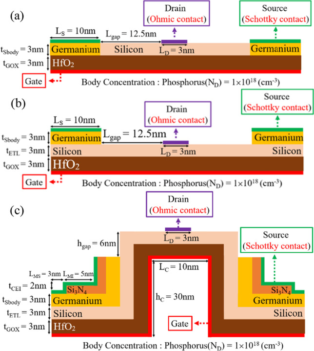
2D schematic of a GS-iTFET, b ETL GS-iTFET, and c CEI ETL GS-iTFET are shown
Fig. 2.
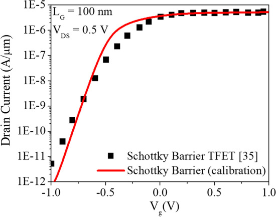
Calibration plot of simulation parameters for the SBTFET
Table 1.
Device parameters used for simulations
| Symbol | Value |
|---|---|
| Source body thickness (tSbody) | 3 nm |
| Epitaxial tunnel layer thickness (tETL) | 3 nm |
| Gate oxide thickness (tGOX) | 3 nm |
| CEI thickness (tCEI) | 2 nm |
| Convex length (Lc) | 10 nm |
| Convex height (hc) | 30 nm |
| Drain metal length (LD) | 3 nm |
| Gap height (hgap) | 6 nm |
| Body doping concentration (phosphorus) | 1 × 1018 cm−3 |
| Schottky barrier | 0.7 eV |
| Gate metal work function | 4.1 eV |
This paper is a simulation work and Fig. 3 shows the assumed manufacturing process of our designed CEI ETL GS-iTFET.
Fig. 3.
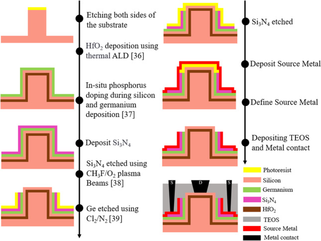
Flowchart of the CEI ETL GS-iTFET manufacturing process
(a) A polycrystalline silicon substrate is used as the back gate electrode. (b) A negative photoresist is used to define the fin shaped structure, followed by dry etching to remove the Polycrystalline silicon. (c) A 3 nm layer of hafnium dioxide is deposited on the polycrystalline silicon as the gate oxide using thermal atomic layer deposition. (d) Silicon and germanium materials are in-situ doped for deposition by high temperature phosphorus evaporation. (e) Low pressure chemical vapor deposition (LPCVD) is used with SiH2Cl2/DCS and NH3 as precursor gases to grow a silicon nitride thin film. (f) Plasma etching with CH3F/O2 is used to etch the nitride and physical etching with Cl2/N2 is used to define the drain region. (g) Positive photoresist is used to define the areas where the metal contacts directly contact the semiconductor. (h) Lift-off technique is used to define the source metal. (i) A protective layer of TEOS is deposited by plasma enhanced chemical vapor deposition (PECVD). (j) Finally, metal interconnects are formed by defining contact windows using a photomask, allowing bias to be applied using probes for measurement purposes.
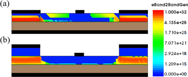
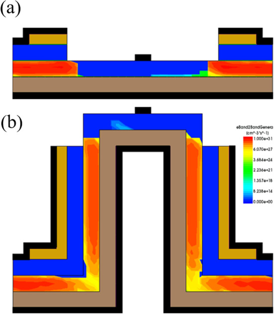
The electron generation rate caused by BTBT in CEI ETL GS-iTFET varies under three different gate bias conditions: (a) ambipolar, (b) OFF-state, and (c) ON-state, with Vd set at 0.2 V, as illustrated in Fig. 4. At Vgs = − 1 V, Fig. 4a shows a negligible ambipolar current caused by a slight parasitic tunneling junction. At Vgs = 0 V, Fig. 4b exhibits a minor corner-point tunneling that has little impact on the overall subthreshold swing. However, in Fig. 4c at Vgs = 1 V, the electron generation rate fills the entire channel, resulting in a powerful tunneling current.
Fig. 4.
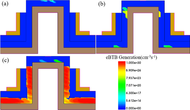
Electron band-to-band generation of the CEI ETL GS-iTFET. a Ambipolar conduction, b OFF-state, and c ON-state
In traditional TFETs, the current is generated through point tunneling, occurring when the tunneling direction is perpendi-cular to the electric field direction at the tunneling point (along the cut line B–B' in Fig. 5b). In contrast, our proposed CEI ETL GS-iTFET generates tunneling current through line tunneling, where the tunneling direction is parallel to the electric field direction (along the cut line A–A' in Fig. 5a). To maximize the number of line tunneling events, we aim to overlap the source and gate regions as much as possible, rather than relying solely on point tunneling. This allows line tunneling dominant TFETs to have higher drive currents than point tunneling dominant TFETs. Figure 5a clearly shows the overlap region of the conduction and valence bands (light blue area), while Fig. 5b does not have such an overlap region. Therefore, we conclude that the CEI ETL GS-iTFET is dominated by line tunneling.
Fig. 5.
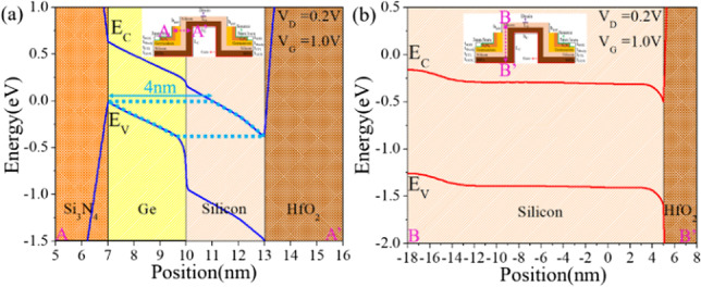
Band diagram of CEI ETL GS-iTFET for a line tunneling (along the cut line A–A') and b point tunneling (along the cut line B–B')
Results and discussion
Optimizing the materials of source and channel regions
Traditional tunnel field effect transistors (TFETs) use single crystal silicon as the body material. However, germanium, which has a narrower bandgap than silicon, offers the potential for higher drive currents. However, the use of pure germanium as the body material leads to a significant increase in leakage current, while pure silicon exhibits limited tunneling due to its wider bandgap. To overcome this challenge, a hybrid approach is proposed where germanium is used in the source region while the channel region is replaced by silicon. This heterojunction configuration takes advantage of the band offset at the interface, resulting in an increased tunneling area between the source and channel in the on-state. Conversely, the wider bandgap of the silicon in the off-state makes tunneling less likely, ensuring low leakage current. This design strategy allows high drive currents to be achieved while maintaining low leakage current [21, 22]. Figure 6 illustrates the superior performance of the device in terms of high Ion/Ioff ratio at low voltage conditions.
Fig. 6.
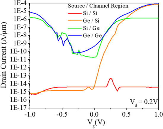
Transfer characteristics of GS-iTFET structure with different Source and Channel Regions materials at Vds = 0.2 V
Effectively prevents point tunneling
In our previous work, the GS-iTFET showed remarkable performance. However, the Schottky contact at the source region induced channel inversion, as shown in Fig. 7a. In addition, applying a positive gate bias resulted in a dense electron accumulation layer on the oxide surface, as shown in Fig. 8. Unfortunately, this configuration led to perpendicular tunneling between the source region and the electron accumulation layer, resulting in a hump as shown in Fig. 9. To overcome this challenge, we introduced an epitaxial tunneling layer (ETL) beneath the germanium source region. The addition of the ETL in Fig. 7b clearly separated the P-type region from the channel region, allowing tunneling only in the parallel direction with respect to the gate electric field. Comparative analysis in Fig. 10a showed a significant increase in lateral point tunneling in the absence of ETL. In contrast, Fig. 10b shows that the presence of ETL effectively suppresses point tunneling while maintaining line tunneling. It should be noted that after successful suppression of point tunneling, the conduction current naturally decreases. Although the on-state current does not retain its previous excellent performance, it exhibits a significantly steep behavior in the subthreshold region. Table 2 shows the SSavg and Ion/Ioff ratio for both structures. It can be seen that the SSavg of the ETL GS-iTFET improved from 74.4 (mV/dec) to 30.6 (mV/dec). However, the conduction current (Ion) is slightly decreased from 6.54 × 10⁻⁵ (A/μm) to 1.77 × 10⁻⁵ (A/μm).
Fig. 7.
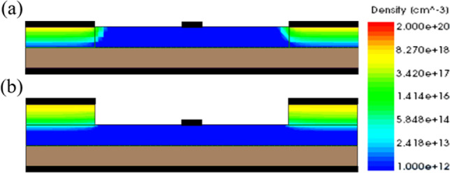
Comparison of hDensity with and without ETL in OFF State at Vgs = 1 V. a GS-iTFET and b ETL GS-iTFET
Fig. 8.
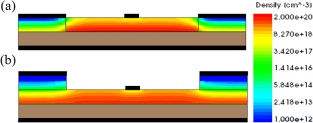
Comparison of eDensity with and without ETL in OFF State at Vgs = 1 V. a GS-iTFET and b ETL GS-iTFET
Fig. 9.
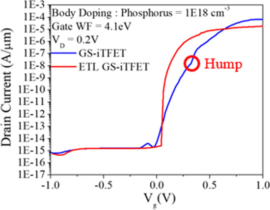
Transfer characteristics with and without ETL
Fig. 10.
Comparison of eBTB Generation with and without ETL at Vgs = 1 V. a GS-iTFET and b ETL GS-iTFET
Table 2.
Comparison of two structures
| GS-iTFET | ETL GS-iTFET | |
|---|---|---|
| VD (V) | 0.2 | 0.2 |
| SSavg (mV/dec) | 74.4 | 30.6 |
| Ion (A/μm) | 6.54 × 10⁻⁵ | 1.77 × 10⁻⁵ |
| Ioff (A/μm) | 2.3 × 10⁻¹⁵ | 2.58 × 10⁻¹⁵ |
| Ion/Ioff Ratio | 2.84 × 10¹⁰ | 6.88 × 10⁹ |
Using charge-enhancement insulation to depinning the Fermi level
In our previous work, we induced minority carrier holes to invert into P-type region in the N-type germanium source using a Schottky contact. However, direct metal contact on a semiconductor can cause Fermi level pinning effect [23], where the Schottky barrier is fixed. Since our device uses Schottky contact instead of ion implantation to create P-type region, fixing the Schottky barrier will limit our device's performance. Therefore, we need to insert a thin insulating layer between the metal and the semiconductor to mitigate the Metal-Induced Gap States (MIGS) effect and achieve Fermi level depinning. We added a 2 nm Si3N4 layer at the metal–semiconductor interface as the Charge-Enhancement Insulation (CEI), as shown in Fig. 1(c). The variations in Schottky barrier height at the metal–semiconductor interface are extracted for the cases without CEI and with Si3N4 layers of 1 nm, 2 nm, and 5 nm, respectively. The pinning factors S are obtained by calculating the slope of the linear regression lines [24]. From Fig. 11, it can be observed that the pinning factor S for the case without Si3N4 layer is 0.064, whereas for the case with a 1 nm Si3N4 layer, the pinning factor S is 0.507. The pinning factor S with CEI is higher than that without CEI, indicating that CEI can effectively alleviate the Fermi level pinning effect. Notably, the pinning factors for Si3N4 layers of 2 nm and 5 nm thickness are 0.502 and 0.253, respectively, both smaller than that for the 1 nm layer, suggesting that a thicker CEI does not necessarily lead to a better depinning effect.
Fig. 11.
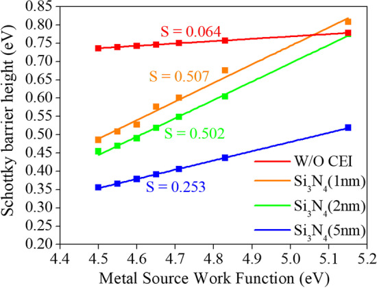
Extracted effective Schottky barrier heights for contacts without CEI, with 1 nm, 2 nm, and 5 nm Si3N4 layers. The S-factors for each case are also shown in the figure
Previously, we reduced the Fermi level pinning effect by adding a 2 nm Si3N4 layer at the metal–semiconductor interface. In addition to reducing the FLP effect, the Si3N4 layer can also reduce the loss of induced minority carrier holes from the metal. As shown in Fig. 12a, b, without an insulating layer, the holes flow out to the source metal in large quantities, resulting in the loss of induced minority carrier holes. On the other hand, with an insulating layer, the loss of holes is reduced, leaving more holes, as shown in Fig. 13. In addition, the increased concentration of induced carriers increases the conduction current, as shown in Fig. 14.
Fig. 12.
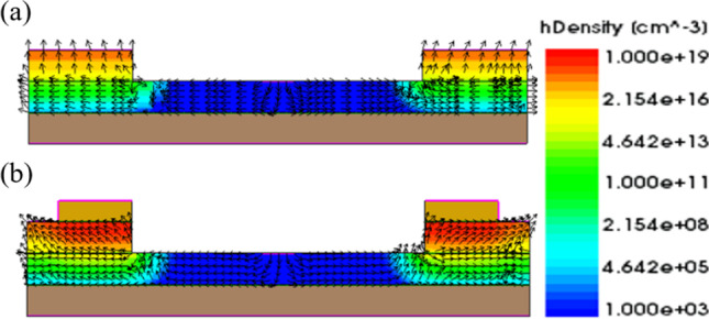
Direction of hole flow with and without the CEI for a W/O CEI and b With CEI at Vgs = 1 V
Fig. 13.
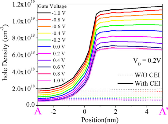
Electron concentration diagrams for the cutting line A to A' are shown for with and without the CEI at various gate voltages
Fig. 14.
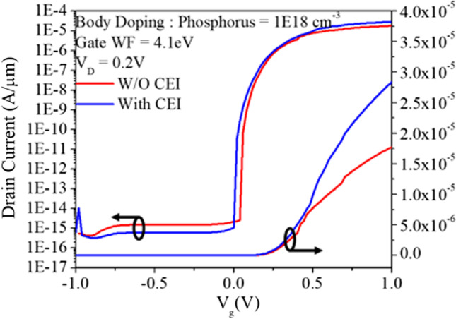
Transfer characteristics with and without the CEI are shown
Figure 15 shows that increasing the source-drain overlap length leads to a greater occurrence of tunneling and consequently increases the on-current as shown in Fig. 16.
Fig. 15.
Comparison of eBTB Generation at different overlap lengths. a Overlap length 16 nm and b overlap length 58 nm
Fig. 16.
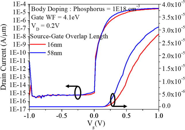
Transfer characteristics at different source-gate overlap lengths
The distance between the source and drain is a critical factor affecting the performance of the device. In this study we investigate the effect of the gap height (hgap) between the source and the top surface and the length (LD) of the drain metal. Figure 17 shows the relationship between LD and leakage current for different hgap values. It can be seen that a shorter hgap results in a higher leakage current as LD increases. Conversely, increasing hgap reduces the leakage current. This phenomenon can be attributed to direct tunneling from the source to the drain when the gap between them is too small, resulting in significant leakage. To ensure optimum electrical characteristics, increasing the hgap allows a longer LD, but at the cost of reduced on-current due to a smaller tunneling area. In addition, the Gate-Induced Drain Leakage (GIDL) effect should be considered when extending the LD. For our device simulation, we set hgap to 6 nm and LD to 3 nm.
Fig. 17.
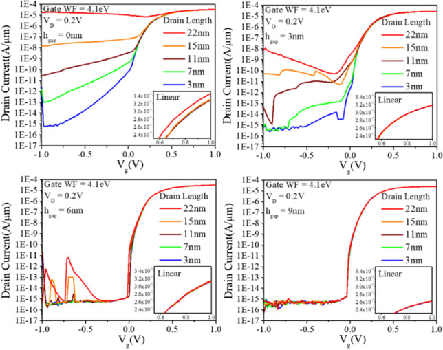
Transfer characteristics of the CEI ETL GS-iTFET. They are analyzed with respect to the modulation of LD at different hgap values
Consideration of practical process defects
During the actual manufacturing process, repeated high-voltage stress can induce defects at interfaces and between different materials. These defects are located in the forbidden energy band between the conduction and valence bands and have the ability to trap carriers, resulting in a two-stage tunneling process that resembles a dormancy point. As a result, the required tunneling barrier is reduced, allowing carriers to more easily pass through the defects from the valence band to the conduction band, thereby increasing the device current. This phenomenon is commonly referred to as trap-assisted tunneling (TAT). However, the effect of TAT on the driving current is limited, while it significantly increases the leakage current. In addition, as device dimensions decrease and the electron mobility within the channel decreases, the on current decreases, as shown in Fig. 18.
Fig. 18.
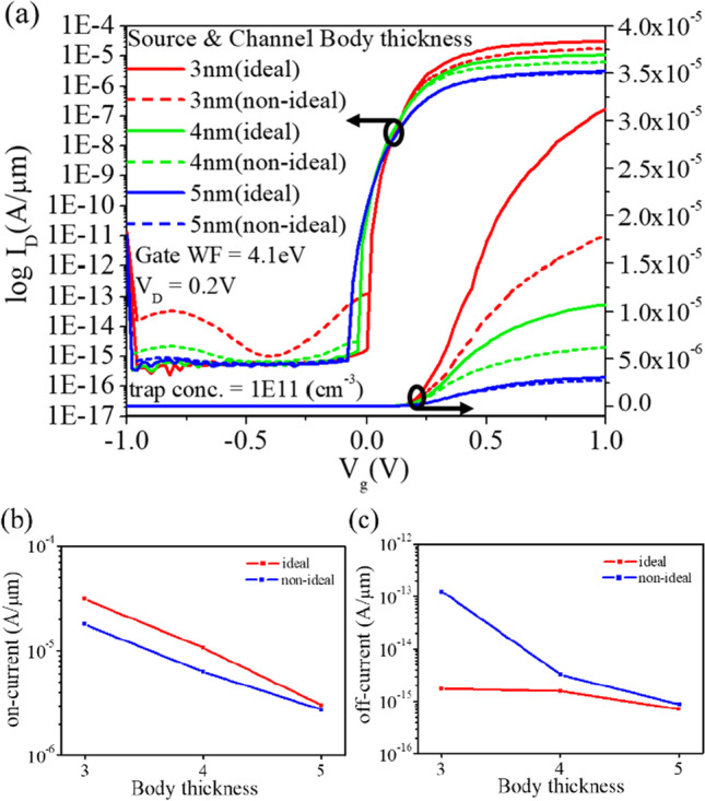
Ideal and non-ideal CEI ETL GS-iTFET with different body thicknesses. a Transfer characteristics, b on-current, c off-current
Temperature is a critical parameter that significantly affects the performance of semiconductor devices. As temperature increases, the bandgap of TFET devices decreases, leading to an increase in the band-to-band tunneling current [25]. However, the effect of temperature on the on-state current is not significant, whereas the off-state current is significantly affected by temperature, as shown in Fig. 19a. This difference is due to the fact that the off-state current is composed of trap-assisted tunneling (TAT) current, band-to-band tunneling (BTBT) current and Shockley–Read–Hall (SRH) recombination current, while the on-state current is mainly composed of BTBT current [26, 27]. From Fig. 19b, it can be observed that the TFET does not exhibit self-heating effects leading to a decrease in current even at high temperatures (500 K). Finally, we present the extracted data of the on-state current, off-state current and average subthreshold swing in Fig. 19c.
Fig. 19.

Temperature modulation of CEI ETL GS-iTFET for a Id–Vg curve, b Id–Vd curve, and c Ion, Ioff current
Due to the extremely small size of our device, we have considered the Quantum Confinement (QC) effect using the quantum momentum model (Density Gradient) [40]. Figure 20 shows the transfer characteristics with and without the use of QC at different semiconductor thicknesses. It is clear that the thinner the semiconductor thickness, the greater the effect.
Fig. 20.
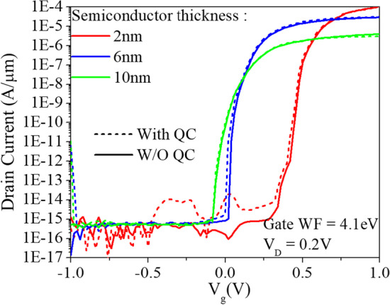
Simulated transfer characteristics of the CEI ETL GS-iTFET with and without Quantum Confinement (Density Gradient) considered
Finally, we conducted an evaluation of our proposed device's performance based on Ion/Ioff Ratio and SS, as illustrated in Fig. 21 [28–34]. Compared to other devices, the ETL GS-iTFET exhibited a remarkable Ion/Ioff Ratio. However, we also had to take into account the issue of FLP. Therefore, while mitigating FLP, the CEI ETL GS-iTFET achieved a slightly better average subthreshold swing compared to the ETL GS-iTFET. It is worth noting that our simulations were performed without ion implantation, which resulted in an excellent performance while significantly reducing the thermal budget. Ultimately, the CEI ETL GS-iTFET demonstrates tremendous potential as one of the most promising candidates for the next generation of low-power devices.
Fig. 21.

Performance comparison of devices. SSavg of TFETs as a function of Ion/Ioff
Conclusion
In this paper, we propose a CEI ETL GS-iTFET structure that uses a Schottky contact instead of ion implantation to induce minority carrier holes in the N-type body, thereby inverting the P-type region. Unlike conventional TFET devices that rely on point tunneling, our device utilizes source-gate overlap to create a line tunneling structure, resulting in a higher on-current. In addition, germanium material is incorporated as the source region to further increase the on-current, while an epitaxial tunnel layer (ETL) serves as the primary tunneling region to reduce the leakage current resulting from point tunneling between the source and drain. To mitigate Fermi level pinning (FLP), a layer of Si3N4 is introduced as charge enhancement isolation (CEI) between the source region and the Schottky metal. This layer effectively minimizes the loss of minority carrier holes and alleviates FLP effects, ultimately improving the efficiency and stability of the device. We also perform simulations to investigate non-ideal effects encountered during the manufacturing process and their impact on device performance. Under ideal conditions, the CEI ETL GS-iTFET exhibits exceptional performance with an average subthreshold swing (SSavg) of 30.5 mV/dec and an Ion/Ioff ratio of 1.81 × 10¹⁰. In summary, our proposed CEI ETL GS-iTFET has great potential to expand the application range of TFT technology and drive future advances in the development of thin film transistors (TFTs) for low power, low voltage and fast switching applications. This technological advancement addresses the demand for high efficiency, superior performance and low power consumption, ultimately improving overall device performance, stability and widespread adoption in future electronic devices.
Author contributions
YCC contributed to Writing, editing, and Data curation. JTL contributed to Conceptualization, Super-vision, Revision, and Project administration. All the authors discussed the results and commented on the manuscript. All authors read and approved the manuscript.
Funding
The funding was provided by Ministry of Science and Technology, Taiwan (MOST-109-2221-E-110-018-MY3, MOST-109-2221-E-110-018-MY3).
Data availability
All the data are available from the corresponding author on reasonable request.
Declarations
Competing interests
The authors declare no competing interests.
Footnotes
Publisher's Note
Springer Nature remains neutral with regard to jurisdictional claims in published maps and institutional affiliations.
References
- 1.Leonelli D, et al. Multiple-gate tunneling field effect transistors with sub-60 mV/dec subthreshold slope. Technical Digest SSDM, 2009. p. 767–8. 10.7567/SSDM.2009.A-4-1.
- 2.Gupta PS, Rahaman H. A phototransistor based on field-effect with bias-dependent mode switching from thermionic to tunneling. In: 2018 International Symposium on Devices, Circuits and Systems (ISDCS); 2018. p. 1–7. 10.1109/ISDCS.2018.8379672.
- 3.Deepjyoti Deb; Rupam Goswami; Ratul Kr Baruah; Kavindra Kandpal; Rajesh Saha, “An SOI n-p-n Double Gate TFET for Low Power Applications,” 2021 Devices for Integrated Circuit (DevIC), 21 June 2021, doi: 10.1109/DevIC50843.2021.9455827.
- 4.The International Roadmap for Devices And SysremTM (IRDS):2018.
- 5.Seo JH, Yoon YJ, Lee HG, Kang IM. Design optimization InGaAs/GaAsSb-based heterojunction Gate-allaround (GAA) arch-shaped tunneling field-effect transistor (A-TFET). In: 2018 International Conference on Electronics, Information, and Communication (ICEIC), Honolulu, HI, USA, 2018. p. 1–2. 10.23919/ELINFOCOM.2018.8330638.
- 6.Leonelli D, Vandooren1 A, Rooyackers1 R, Verhulst AS, De Gendt S, Heyns MM, Groeseneken G. Multiplegate tunneling field effect transistors with sub-60 mV/dec subthreshold slope. 2009 SSDM. 2009. p. 767–8. 10.7567/SSDM.2009.A-4-1.
- 7.Bera PK, Kar R, Mandal D. Design and performance assessment of GaSb/Si heterojunction vertical TFET with delta doped layer for enhanced DC and AF/RF characteristics. In: 2023 International Conference for Advancement in Technology (ICONAT), Goa, India; 2023, p. 1–5. 10.1109/ICONAT57137.2023.10080244.
- 8.Ke S, Hu J, Xu X, "Independent-Gate P-Type TFETs using Double Heterojunction Structures,", IEEE International Symposium on Circuits and Systems (ISCAS) Sapporo, Japan. 2019;2019:1–5. doi: 10.1109/ISCAS.2019.8702154. [DOI] [Google Scholar]
- 9.Skachkov D, Liu S-L, Wang Y, Zhang X-G, Cheng H-P. First-principles theory for Schottky barrier physics. Phys Rev B. 2021;104:045429. doi: 10.1103/PhysRevB.104.045429. [DOI] [Google Scholar]
- 10.Kim JH, Kim S, Park B-G. Double-gate TFET with vertical channel sandwiched by lightly doped Si. IEEE Trans Electron Devices. 2019;66(4):1656–1661. doi: 10.1109/TED.2019.2899206. [DOI] [Google Scholar]
- 11.Gupta A, Chiang CK, Yang WY, Hsieh ER, Chung SS, "Design of Low Voltage Vertical Channel Face-tunneling TFET Using Ge, SiGe Materials and Its SRAM Circuit Performance,", International Symposium on VLSI Technology, Systems and Applications (VLSI-TSA) Hsinchu, Taiwan. 2020;2020:132–133. doi: 10.1109/VLSI-TSA48913.2020.9203664. [DOI] [Google Scholar]
- 12.Connelly D, Faulkner C, Clifton PA, Grupp DE. Fermi-level depinning for low-barrier Schottky source/drain transistors. Appl Phys Lett. 2006;88(1):012105. doi: 10.1063/1.2159096. [DOI] [Google Scholar]
- 13.Janardhanam V, Yun H-J, Jyothi I, Yuk S-H, Lee S-N, Won J, Choi CJ. Fermi-level depinning in metal/Ge interface using oxygen plasma treatment. Appl Surface Sci. 2019;463:91–95. doi: 10.1016/j.apsusc2018.08.187. [DOI] [Google Scholar]
- 14.Chen K-Y, Su C-C, Chou C-P, Wu Y-H. Formation of ohmic contact with low contact resistance on n-GeSn by Fermi level depinning using plasma treatment. IEEE Electron Device Lett. 2016;37(7):827–830. doi: 10.1109/LED.2016.2566809. [DOI] [Google Scholar]
- 15.Lieten RR, Afanas'ev VV, Thoan NH, Degroote S, Walukiewicz W, Borghs G. Mechanisms of Schottky barrier control on n-type germanium using Ge3N4 interlayers. Electrochem Soc J. 2011;15(4):8. doi: 10.1149/1.3545703. [DOI] [Google Scholar]
- 16.Avci UE, Morris DH, Young IA. Tunnel field-effect transistors: prospects and challenges. IEEE J Electron Devices Soc. 2015;3(3):88–95. doi: 10.1109/JEDS.2015.2390591. [DOI] [Google Scholar]
- 17.Krishnamohan T, Kim D, Raghunathan S, SaraswatDouble-Gate Strained-Ge Heterostructure Tunneling FET (TFET) With record high drive currents and ≪60mV, dec subthreshold slope K. IEEE International Electron Devices Meeting. San Francisco, CA, USA. 2008;2008:1–3. 10.1109/IEDM.2008.4796839.
- 18.Liu M, Xie Q, Xia S, Wang Z, A novel step-shaped gate tunnel FET with low ambipolar current. 2nd International Symposium on Devices, Circuits and Systems (ISDCS). Higashi-Hiroshima, Japan. 2019;2019:1–4. 10.1109/ISDCS.2019.8719250.
- 19.Singh P, Chauhan VK, Ray DD, Dash S, Mishra GP, “Ambipolar Performance Improvement of Dual Material TFET Using Drain Underlap Engineering,”,. IEEE Electron Devices Kolkata Conference (EDKCON). Kolkata, India. 2018;2018:274–7. 10.1109/EDKCON.2018.8770478.
- 20.Sentaurus Device User Guide Synopsys Inc., 2020.
- 21.Takeda H, Yamamoto T, Ikezawa T, Kawada M, Takagi S, Hane M. Impact of source-to-channel carrier injection properties on device performance of sub-100nm metal source/drain Ge-pMOSFETs. Symposium on VLSI Technology. 2008;2008:58–59. doi: 10.1109/VLSIT.2008.4588563. [DOI] [Google Scholar]
- 22.Vanlalawpuia K, Bhowmick B. Investigation of a Ge-source vertical TFET with delta-doped layer. IEEE Trans Electron Devices. 2019;66(10):4439–4445. doi: 10.1109/TED.2019.2933313. [DOI] [Google Scholar]
- 23.Khan A, Din HU, Idrees M, Khan F, Alrebdi TA, Nguyen CV, Shafiq M, Amin B. First principles study of metal-semiconductor contact between MX2 (M = Nb, Pt; X = S, Se) monolayers. Phys Lett A. 2019 doi: 10.1016/j.physleta.2019.125867. [DOI] [Google Scholar]
- 24.Tsui B-Y, Kao M-H. Mechanism of Schottky barrier height modulation by thin dielectric insertion on ntype germanium. Appl Phys Lett. 2013;103:032104. doi: 10.1063/1.4813834. [DOI] [Google Scholar]
- 25.Der Agopian PG, Martino JA, Rooyackers R, Vandooren A, Simoen E, Claeys C. Experimental comparison between trigate p-TFET and p-FinFET analog performance as a function of temperature. IEEE Trans Electron Devices. 2013;60(8):2493–2497. doi: 10.1109/TED.2013.2267614. [DOI] [Google Scholar]
- 26.Chander S, Sinha SK, Kumar S, Singh PK, Baral K, Singh K, Jit S. Temperature analysis of Ge/Si heterojunction SOI-Tunnel FET. Superlattices Microstructures. 2017;110:162–170. doi: 10.1016/j.spmi.2017.08.048. [DOI] [Google Scholar]
- 27.Narang R, Saxena M, Gupta RS, Gupta M. Impact of temperature variations on the device and circuit performance of tunnel FET: a simulation study. IEEE Trans Nanotechnol. 2013;12(6):951–957. doi: 10.1109/TNANO.2013.2276401. [DOI] [Google Scholar]
- 28.Song W, et al. Steep subthreshold swing in GaN negative capacitance field-effect transistors. IEEE Trans Electron Devices. 2019;66(10):4148–4150. doi: 10.1109/TED.2019.2934181. [DOI] [Google Scholar]
- 29.Kim HW, Kwon D. Gate-normal negative capacitance tunnel field-effect transistor (TFET) With channel doping engineering. IEEE Trans Nanotechnol. 2021;20:278–281. doi: 10.1109/TNANO.2021.3068572. [DOI] [Google Scholar]
- 30.Ko E, Lee H, Park J-D, Shin C. Vertical tunnel FET: design optimization with triple metal-gate layers. IEEE Trans Electron Devices. 2016;63(12):5030–5035. doi: 10.1109/TED.2016.2619372. [DOI] [Google Scholar]
- 31.Gupta M, Hu VP-H. Negative capacitance junctionless device with mid-gap work function for low power applications. IEEE Electron Device Lett. 2020;41(3):473–476. doi: 10.1109/LED.2020.2969210. [DOI] [Google Scholar]
- 32.Hu VP-H, Lin H-H, Lin Y-K, Hu C. Optimization of negative-capacitance vertical-tunnel FET (NCVT-FET) IEEE Trans Electron Devices. 2020;67(6):2593–2599. doi: 10.1109/TED.2020.2986793. [DOI] [Google Scholar]
- 33.Kim HW, Kwon D. Steep switching characteristics of L-shaped tunnel FET with doping engineering. IEEE J Electron Devices Soc. 2021;9:359–364. doi: 10.1109/JEDS.2021.3066460. [DOI] [Google Scholar]
- 34.Guan Y, Li Z, Zhang W, Zhang Y, Liang F. A full-range analytical current model for heterojunction TFET with dual material gate. IEEE Trans Electron Devices. 2018;65(11):5213–5217. doi: 10.1109/TED.2018.2870171. [DOI] [Google Scholar]
- 35.Kim HW, et al. Schottky barrier tunnel field-effect transistor using spacer technique. J Semicond Technol Sci. 2014;14(5):572–578. doi: 10.5573/JSTS.2014.14.5.572. [DOI] [Google Scholar]
- 36.Lee K-M, Ju B-K, Choi S-H. a-InGaZnO thin-film transistors with novel atomic layer-deposited HfO2 gate insulator using two types of reactant gases. IEEE Trans Electron Devices. 2023;70(1):127–134. doi: 10.1109/TED.2022.3223322. [DOI] [Google Scholar]
- 37.Chaung I, Michael A, Kwok CY. Study and application of in-situ phosphorus doped thick polysilicon films at low temperature for post CMOS-MEMS integration. In 2019 IEEE 32nd International Conference on Micro Electro Mechanical Systems (MEMS), Seoul, Korea (South); 2019. p. 299–302. 10.1109/MEMSYS.2019.8870724.
- 38.Kaler SS, Lou Q, Donnelly VM, Economou DJ. Silicon nitride and silicon etching by CH3F/O2 and CH3F/CO2 plasma beams. Department of Chemical and Biomolecular Engineering, 2016. 10.1116/1.4949261.
- 39.Castro MSB, Barnola S, Glück B. Selective and anisotropic dry etching of Ge over Si. J Integ Circuits Syst. 2013 doi: 10.29292/jics.v8i2.380. [DOI] [Google Scholar]
- 40.Anvarifard MK, Orouji AA. Energy band adjustment in a reliable novel charge plasma SiGe source TFET to intensify the BTBT rate. IEEE Trans Electron Devices. 2021;68(10):5284–5290. doi: 10.1109/TED.2021.3106891. [DOI] [Google Scholar]
- 41.Yoon J-S, Kim K, Meyyappan M, Baek C-K. Bandgap engineering and strain effects of core-shell tunneling field-effect transistors. IEEE Trans Electron Devices. 2018;65(1):277–281. doi: 10.1109/TED.2017.2767628. [DOI] [Google Scholar]
Associated Data
This section collects any data citations, data availability statements, or supplementary materials included in this article.
Data Availability Statement
All the data are available from the corresponding author on reasonable request.