

Abstract
Ultrafast optical microscopy, generally employed by incorporating ultrafast laser pulses into microscopes, can provide spatially resolved mechanistic insight into scientific problems ranging from hot carrier dynamics to biological imaging. This Review discusses the progress in different ultrafast microscopy techniques, with a focus on transient absorption and two-dimensional microscopy. We review the underlying principles of these techniques and discuss their respective advantages and applicability to different scientific questions. We also examine in detail how instrument parameters such as sensitivity, laser power, and temporal and spatial resolution must be addressed. Finally, we comment on future developments and emerging opportunities in the field of ultrafast microscopy.
Introduction
Ultrafast optical microscopy is based on spectroscopy techniques that use sequences of ultrashort light pulses to study material properties and have attracted considerable attention in the past few decades due to their ability to resolve short-lived intermediates on the order of femtoseconds.1−3 Femtosecond temporal resolution was first achieved in studies of the dynamics of organic molecules and bond breakages in iodine cyanide molecules.4−6 Following this breakthrough, ultrafast optical spectroscopy has been utilized in a multitude of disciplines based on light ranging from X-rays to terahertz radiation and have led to countless scientific insights.7−17 The discussion of all these fields of study is well beyond the scope of this work, but excellent reviews can be found in the literature.18−24 Instead, here we discuss few examples in the infrared (IR) but focus on the visible (VIS) part of the spectrum, where ultrafast optical spectroscopy has been applied for biological and life science applications as well as studies of chemical reactions, solvation dynamics, and nanomaterials.25−35 As a result, tremendous insights into the electronic dynamics of various materials have been achieved, and technological advances in the generation and manipulation of ultrashort light pulses in the VIS as well as interdisciplinary exchange continue to expand the capabilities of ultrafast optical spectroscopy in this spectral regime.36−40
However, ultrafast optical spectroscopy techniques generally lack the spatial resolution to perform studies within nanometer-scaled material areas or conduct measurements of single-particles on the nanoscale or smaller. The importance of spatial resolution has been shown by optical far-field microscopy in the VIS, which provides the ability to spatially resolve location-dependent photoexcited processes in heterogeneous materials or identify particle-to-particle variations in single-particle measurements.41,42 Utilizing VIS optical far-field microscopy, studies demonstrated a significant dependence of the properties of a material on its size, shape, environment, or the specifically inspected material area.43−46 Importantly, bulk or ensemble measurements often hide contributions from spatial heterogeneity due to averaging effects, making mechanistic studies difficult.47 Thus, there is a need to achieve high spatial resolution in addition to the chemical and temporal sensitivity of ultrafast optical spectroscopy techniques, motivating the development of the corresponding ultrafast optical microscopy techniques.
Ultrafast optical microscopy for VIS wavelengths was realized by pairing the spatial resolution and high detection sensitivities of VIS far-field optical microscopy with well-established ultrafast spectroscopic techniques such as VIS transient absorption (TA), and, more recently, two-dimensional (2D) ultrafast spectroscopy.48−54 The resulting methods have become crucial tools in studying ultrafast dynamics of zero- or one-dimensional materials such as single molecules, metal nanoparticles, semiconducting quantum dots, or carbon nanotubes.55−67 Furthermore, VIS ultrafast optical microscopy was applied to study local areas of two-dimensional heterogeneous chemical systems such as organic semiconducting thin films and polycrystalline perovskite thin films64,68−80 and biological media such as cells or chromophores.51,81−86
This Review will highlight the crucial role of ultrafast optical microscopy in the VIS regime in resolving and understanding the impact of microscopic heterogeneity on physical and chemical processes. We will use examples from the literature to showcase implementations of ultrafast TA and 2D microscopy in the VIS, discuss their advantages and disadvantages, and highlight their benefit over the corresponding spectroscopy techniques. We also provide a guide on the appropriate choice of ultrafast optical microscope instrument parameters for different sample types, since the experimental demands for ultrafast optical microscopy measurements sensitively depend on the nature of the sample. We here provide a nonextensive review of the fundamental principles and technical details of ultrafast optical TA microscopy and 2D microscopy as applied in the VIS and mid-IR wavelength ranges, as many excellent comprehensive reviews are already available.18,19,87−100 Please note that we will refer to ultrafast optical microscopy and spectroscopy techniques in the VIS simply as ultrafast optical microscopy and spectroscopy if not otherwise stated, because we focus on this section of the electromagnetic spectrum.
That said, we also note that there are alternative ways to employ ultrafast optical microscopy that can achieve extremely high spatial resolution down to a few nanometers. These approaches use nonoptical mechanisms in addition to light pulses and include methods such as ultrafast scanning-tunneling microscopy (ultrafast STM),101−103 pump–probe atomic force microscopy (ultrafast AFM),104−108 ultrafast electron microscopy (UEM),109−112 and ultrafast near-field scanning optical microscopy (ultrafast NSOM),113 among others.114 While these techniques have provided important information to the scientific community, they are not the focus of this Review. However, following the theme of this review we want to indicate their instrumental similarities and differences, as well as capabilities and limitations compared to the corresponding all-optical techniques. We will thus only briefly discuss ultrafast STM in the VIS regime as an example and comment on UEM.
The Review is organized as follows: We first introduce a brief practical overview of the experimental techniques of ultrafast TA microscopy, 2D microscopy, and STM. We then discuss how appropriate instrument parameters such as the laser repetition rate, or temporal and spatial resolution must be chosen for different materials and phenomena. With this basis, we discuss some state-of-the-art applications of ultrafast microscopy and highlight their scientific insights as well as unique instrument developments. Lastly, we comment on current challenges in ultrafast optical microscopy and suggest future directions.
Practical Overview of Experimental Techniques
Transient Absorption Microscopy
As discussed above, TA microscopy was developed by coupling conventional TA spectroscopy with a far-field microscope.57,58,75,78,115 As a general approach in TA microscopy measurements, two laser pulses, a pump and a probe, pulse interrogate a sample either in a transmission or reflection geometry.50,116Figure 1A provides a schematic of a TA microscopy setup in transmission geometry. The pump pulse promotes the material under investigation to an excited state. The following probe pulse measures the dynamics of those excited and short-lived states through changes in the absorption, reflection, or excited state emission that are measurable through modulation of the intensity of the transmitted or reflected probe beam.40 By inserting a time delay on the order of femtoseconds to nanoseconds between pump and probe pulses, it is then possible to probe the dynamic behavior of a sample at ultrashort times after the initial excitation. Considering a transmitted probe beam, the measured signal is usually provided as the differential transmission ΔT/T, corresponding to the ratio of the change in transmission due to the sample being excited (ΔT) relative to the total transmission when the sample is in its ground state (T). Similarly, the differential reflection ΔR/R is measured for reflection geometries.
Figure 1.

(A) Schematic of a collinear setup for TA microscopy. Pump (blue) and probe (red) pulses are recombined with a dichroic optic and travel along the same path, offset in time by a delay t. Both beams are focused onto a sample through an objective. The probe pulse, which carries the encoded TA signal, is isolated from the pump using spectral or polarization filters and is measured by a detector. For detection of small signals, the pump is modulated using a chopper or AOM and pump-induced changes in the transmission of the probe through the sample are automatically extracted through lock-in amplification. DM: Dichroic optic. M: Mirror. F: Filter. (B) Simplified schematics of different imaging techniques in ultrafast TA microscopy. Left: Sample scanning with a piezo translation stage. Center: Beam scanning with piezo-electric mirrors. Right: Imaging of a sample area with defocused beams.
The temporal delay between the two pulses is usually controlled via a mechanical delay stage that alters the traveled distance of either the pump or the probe.92 Though challenging, delay times close to 10 ns can be achieved by passing the beam through the delay stage multiple times. Other studies have utilized digital delay generators to control the time delay between pulses.117 New approaches have also applied asynchronous optical sampling techniques, in which two laser sources produce pump and probe pulses with different repetition rates to generate a periodically changing temporal delay.118 The latter methodology has the advantage that long delay times up to tens of nanoseconds can be accomplished by simply adjusting the laser repetition rates. However, this approach requires high temporal synchronization and stability of the laser systems.
In TA microscopy, pump and probe beams are generally spatially overlapped and focused onto the sample, usually using an objective with a high numerical aperture (NA) to achieve small focus spot sizes from the micrometer scale down to the optical diffraction limit of a few hundred nanometers. Small beam spot sizes are important for TA microscopy measurements because ΔT/T is inversely proportional to the area of the focused probe beam.91 Additionally, the minimum spot size determines the spatial resolution. After the sample, the transmitted or reflected pump pulse, depending on the measurement geometry, is subsequently removed through either spatial separation or filtering based on wavelength or polarization, and only the probe is detected.57,119−122
Due to the small size of single nanoparticles or single molecules, even beam spot sizes close to the diffraction limit are much larger than the sample, and the signal-to-noise ratio is too low to measure the differential transmission directly. One method to address this challenge is lock-in amplification, in which the pump beam is chopped at frequencies between a few Hz up to tens of kHz or hundreds of kHz by either a mechanical chopper or an acoustic optical modulator (AOM), respectively.123,124 The modulation frequency is then referenced to the detection system to extract signal components with matching oscillations from the background. The detection system is usually either an array detector such as a charge-coupled device (CCD) camera or a single-element detector. In the former case, the pump modulation is directly referenced to the CCD camera for lower frequencies, while for the latter the single-element detector is connected to a lock-in-amplifier that is synchronized to the modulation frequency. The lock-in amplification approach is a common practice, especially with higher repetition rate laser sources as it provides large signal-to-noise ratios for nanoscale samples.125,126 Spectral resolution of the TA signal can additionally be realized by incorporating a spectrograph into the detection system.127
Finally, a TA image can be obtained by scanning a sample through the laser beam with a piezo nanopositioning stage, scanning the pump and probe beams over the sample using galvano-scanning mirrors, or through wide-field geometries with defocused probe beams, as shown in Figure 1B.59,64,128 Temporally resolved TA images are achieved by varying the time delay between pump and probe beams between subsequent images, and time-resolved transients are taken by scanning through multiple delay times at a fixed sample location.
Ultrafast Two-Dimensional Microscopy
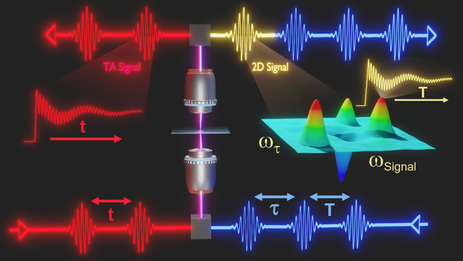
Ultrafast 2D microscopy has been developed to provide both spatial and temporal insights into the dynamics of materials, and is similar to TA microscopy in much of its instrumentation.53,90,129,130 Ultrafast 2D microscopy distinguishes itself from TA microscopy by the detected signal and by mapping spectroscopic information over two frequency axes, usually accomplished using three laser pulses; two pump pulses and one probe pulse, as shown in Figure 2A.129 One of the pump pulses is referred to as the stationary pulse, and the other is called the traveling pulse. The traveling pulse is scanned through different time delays relative to the stationary pulse. The effect of these pump pulses can be interpreted as the preparation of a superposition of excited and ground states. At each pump–pump time delay (τ), the probe pulse interacts with the optically pumped sample after an additional pump–probe time delay (T), during which the population states are allowed to evolve. The effect of the probe pulse is to generate a nonlinear, third-order macroscopic polarization in the sample, leading to a detectable signal field that is coherently radiated by the individual dipoles in the sample.52 The first frequency axis, called the probe axis, is generated by spectrally resolving this signal field in a grating spectrometer. The second frequency axis, called the pump axis, comes from Fourier transformation of the signal fields that were obtained for the different pump–pump time delays (τ) at each probe frequency.
Figure 2.

(A) Schematic of a collinear setup for ultrafast 2D microscopy. An AOM or chopper is used to modulate the pump beam. When using white-light pulses, thin film polarizers are used to recombine pump and probe pulses onto the same path based on their polarization rather than wavelength. The two pump pulses are offset by a time τ, and the probe pulse is offset from the last pump pulse by an additional time T. Both beams are focused onto a sample through an objective. After removal of the pump beams using a thin film polarizer, interference between the emitted signal field and probe beam is detected using a spectrometer. (B and C) Schematics illustrating the information content of a 2D spectrum. 2D spectra correlate the frequency of the emitted signal with the frequency of the field that excited the sample. This approach can be used to identify peaks in congested absorption spectra by spreading them across 2 frequency axes (B) or to identify coupling or energy transfer between quantum states through the presence of cross peaks that appear away from the diagonal axis (C).
Spreading the spectroscopic information across two different frequency axes provides a wealth of information by deconvolution of congested spectra, permitting signatures of interacting spectral features to be resolved (Figure 2B). Specifically, Figure 2C displays how two axes allow for the distinction between diagonal peaks that lie on the diagonal, where pump and probe frequencies are the same, and cross peaks. Cross peaks lie off the diagonal and result from two interacting spectral features. The interaction can occur through a variety of mechanisms such as electronic coupling, vibrational coupling, or energy transfer processes. 'Similar to TA microscopy, dynamic processes such as energy transfer of solvent rearrangement can be studied by scanning the time delay T between the second pump and probe pulses.131−136 Therefore, ultrafast 2D microscopy holds unique promise for expanding the range of accessible scientific questions beyond the capabilities of TA microscopy.
The addition of a second pump pulse, as well as complicated detection and analysis schemes, can make ultrafast 2D microscopy more experimentally difficult to implement relative to TA microscopy. A general challenge in ultrafast 2D techniques is to obtain absorptive or dispersive spectra with sufficiently low background and high signal-to-noise ratios.18 In order to isolate the required signal fields, ultrafast 2D spectroscopy has employed phase-matching conditions in boxcar geometries, where all pump and probe pulses are focused onto the sample with different wave vectors, leading to signal fields that are emitted with different, defined wave vectors to form the desired spectra.90,137 Additionally, pump–probe geometries have been applied in which both pump pulses travel along the same wave vector, and pump-induced changes in the optical density of a sample were measured using broadband probe pulses that were then spectrally resolved by the detector.138,139 Modulation of the pump with optical choppers allowed reduction of the probe background, and pump pulse pairs were generated using pulse shapers. Pulse shapers modify an initial pulse to generate a pulse pair with variable time delays and relative phase.
High NA objectives complicate phase-matching conditions between pump and probe pulses with different wave vectors, and the boxcar geometry is not appropriate for ultrafast 2D microscopy. Indeed, ultrafast 2D microscopy has predominantly been performed in a fully collinear pump–probe geometry that allows ideal focus of pump and probe beams onto the sample. In these studies, reduced residual background and sufficient signal-to-noise ratios were achieved through combinations of polarization control, additional modulation of the probe, high-frequency light sources, heterodyne detection with an additional pulse, phase cycling, and rotating frame detection.52,53,129,140,141 Phase cycling is a technique used to remove unwanted signal contributions and increase the signal-to-noise of a 2D spectrum, while rotating frame detection allows under-sampling of the signal for shorter measurement times. Both techniques can be conveniently done through pulse shapers, and further information can be found in the literature.90,142
Ultrafast Scanning Tunneling Microscopy
TA and ultrafast 2D microscopy techniques have the ability to measure dynamics of nanometer-sized objects with femtosecond time-resolution. However, owing to their all-optical excitation and detection, their spatial resolution is limited by the diffraction limit of light. Therefore, novel ultrafast techniques such as ultrafast STM have been developed where the probing mechanism is nonoptical, which allows temporal dynamics to be resolved with a spatial resolution of just a few nanometers.143 Consequently, it is possible to measure the dynamics of single molecules,144 nanometer-sized particles,145 or highly heterogeneous low-dimensional materials with superior spatial precision.146 For example, ultrafast STM has been used to detect variations in the electronic structure of individual nanoparticles and interactions between adjacent particles with nanometer-scale resolution.143,145
The principle of ultrafast time-resolved single molecule absorption microscopy by STM (tr-SMA-STM) is similar to that of TA microscopy in that it uses optical pulses in a pump–probe geometry to excite a sample. The pump and probe beams excite micrometer-scale areas of the surface of a sample, but the detected signal is the STM tunneling current as the STM tip is raster-scanned over the sample surface to generate an image (Figure 3).145 Thus, in tr-SMA-STM, the spatial resolution is dependent on the tip resolution, not on the area illuminated by the laser pulses. The tunneling current is detected at the sum frequency of the externally modulated pump and probe beams to achieve high sensitivity in just a few milliseconds of signal averaging at each point on the sample. The tunneling current contains information about how the probe beam depletes excited-state electron density generated by the pump beam, thus unblocking the tunneling of electrons through excited state orbitals. The experiment grants access to femtosecond changes in orbital occupancy of photoexcited processes.147 Due to the small magnitude of the changes in STM current for single molecules or nanoparticles, techniques to modulate the pump pulse dispersion, amplitude, repetition rate, and polarization have been developed to allow for lock-in detection.148 Therefore, ultrafast STM grants spatial resolution beyond the capabilities of ultrafast TA and 2D microscopy while offering the sensitivity to measure excited state kinetics of single nanoscale objects.
Figure 3.

Experimental setup for tr-SMA–STM.145 A femtosecond Ti:sapphire oscillator is split to form pump and probe pulses. The frequency-doubled pump beam is generated by second-harmonic generation, SHG. The pump and probe beams are then modulated on/off at different frequencies and sent collinearly to the tip–sample junction. The tunneling current signal from the STM is demodulated at the sum frequency of the beam modulation by a lock-in amplifier and mapped with subnanometer spatial resolution and femtosecond pump–probe resolution as the tip rasters across the surface. The delay line sets the pump–probe delays. Each image pixel is typically sampled for a few milliseconds at each pump–probe delay. The output of tr-SMA–STM is a series of images at the pump–probe delay times, illustrating how the tunneling current evolves due to the pump–probe sequence. DM = dichroic mirror; M = mirror; PD = photodiode. Adapted from ref (145). Copyright 2021 National Academy of Science.
Experimental Parameters in Ultrafast Optical Microscopy
Depending on the sample of interest or the investigated physical or chemical process, various parameters must be considered for the design of an ultrafast microscopy setup. The choice of instrument components, such as objectives and detectors, affects the capabilities of the microscope, specifically the signal-to-noise ratio, spatial and temporal resolution, and measurement acquisition time. Several different detection schemes, which will be discussed later, have been developed to control these parameters. But, most importantly, the choice of the laser source itself is of great significance as it dictates the pulse energy, repetition rate, pulse duration, and power stability of the pump and probe pulses. These properties, in turn, affect the applicability of other instrument components. As such, ultrafast laser sources have been deterministic in the evolution of ultrafast optical microscopy techniques, and a diverse and versatile range of laser sources have been implemented to address different experimental demands. We want to reemphasize that, while this review focuses on the VIS regime, variations of ultrafast microscopy have been performed using ultrafast laser sources that extend over a range from terahertz to X-ray radiation.20,149−153 Each wavelength region is the basis for different ultrafast microscopy disciplines that allow the study of different material properties, and come with varying instrumental setup requirements.
In the VIS, the multitude of modern laser systems can make the selection of an appropriate laser source challenging. Aiming to provide support in this decision, we let our discussion of scientific insights through ultrafast microscopy be guided by the respectively employed laser sources. We intend to address the question of which type of laser source should be employed to study a specific scientific phenomenon in a given target sample. Below, we define three groups of laser sources that we will reference throughout this review and for which we will discuss appropriate applications.
Amplified laser sources with low repetition rates between 1 and 10 kHz and high pulse energies are ideal for samples such as micrometer-scale, homogeneous two-dimensional materials that require only limited spatial resolution and provide high signal without extended averaging. These sources have been primarily based on amplified Ti:sapphire lasers.69,70,115 One major advantage of these laser sources is their ability to generate pump and probe pulses of various wavelengths. The high pulse energies can be used for nonlinear processes such as super continuum white light generation by pumping sapphire or CaF2 crystals or generating a broad and tunable range of wavelengths using an optical parametric amplifier (OPA).154−156 Due to the low repetition rate and the consequently long time between pulses, these lasers enable studies of slow dynamics that occur on time scales up to hundreds of microseconds. Amplified lasers have thus been employed to investigate a variety of phenomena lasting between several tens of femtoseconds to a millisecond.115,117,157−162 However, because of the high pulse energies, the pump and probe beams require large focal spots on the order of micrometers to avoid laser-induced damage of the sample. Therefore, the use of high NA objectives is limited, adversely affecting the spatial resolution and hence making microscopic studies of samples with sizes close to the diffraction limit difficult. Also important to consider is the reduced sensitivity compared to laser sources with higher repetition rates as the smaller number of pulses per acquisition time provides less opportunity for averaging unless the total measurement time is increased. Previously reported sensitivities of microscopes based on amplified 1–10 kHz laser sources did not exceed differential transmission or reflection values on the order of 10–5, limiting their use to samples producing larger signal levels.70,156
When variable pump and probe wavelengths and also spatial resolution below a micrometer are required, laser sources with repetition rates of hundreds of kHz are advantageous. These laser sources are typically based on Ti:sapphire or Ytterbium as the active laser medium and are often employed in ultrafast optical microscopy.68,163 The higher repetition rate compared to the previously discussed laser systems yields improved signal-to-noise ratios due to averaging and allows for exploration of a wider range of samples with smaller signal levels.163−166 The pulse energies of lasers with hundreds of kHz repetition rate are still high enough to generate variable wavelengths through nonlinear crystals and OPAs.68,74 Short pulse durations of sub 10 fs for both pump and probe beam have been accomplished, hence enabling high time-resolution.74 Since the pulse energy is reduced compared to 1–10 kHz laser sources, objectives with a higher NA can be used to achieve smaller spot sizes on samples of similar laser damage threshold, and spatial resolution near the diffraction limit has been reported.74
For samples with lower signal levels (<10–5) or demand for high spatial resolution, MHz repetition rate lasers are the workhorse in ultrafast optical microscopy. By combining low pulse energies with high repetition rates, these lasers have greatly enhanced measurement sensitivities while avoiding sample damage.50,59,60,167 Utilizing these lasers with tens of MHz repetition rates, signal levels on the order of 10–7 have been detected by virtue of the signal averaging advantage that these sources offer.124 This sensitivity allows for investigating systems such as single nanoparticles and, more recently, single molecules.168,169 The reduced pulse energy enables use of high NA objectives and grants high spatial resolution down to the diffraction limit of light. However, reduced powers also make the utilization of nonlinear effects for tunable wavelength generation more challenging. To gain the necessary wavelength tunability to probe different optical transitions, MHz sources have been frequency doubled by second harmonic generation and coupled to optical parametric oscillators (OPOs). Furthermore, the long-standing challenge of super continuum white-light generation using unamplified MHz oscillators has been overcome in recent years through the use of photonic crystal fibers, which allow the spectral content of pump and probe pulses to be tuned.37,120,124,170,171
Lastly, the applied detector is highly dependent on the utilized laser source and the intended application, as well, and is extremely important for success. Commonly applied detectors are CCD cameras, complementary metal–oxide semiconductor (CMOS) cameras,115 and single-element detectors such as photodiodes,124 avalanche photodiodes (APD),68 and photomultipliers (PMT).69 In each case, the bandwidth of the detector is an important criterion as it dictates if every pulse can be resolved as required in shot-to-shot measurements at lower repetition rates, or if multiple pulses are averaged during signal acquisition. If small signals are expected, the ability to perform lock-in amplification or signal amplification as in electron-multiplying CCD (EMCCD) cameras, APDs, and PMTs can be crucial. When spectral information is required, array detectors such as CCD and CMOS cameras in combination with spectrographs are typically used. Depending on the wavelength range needed for a particular experiment, the detector material must be considered, with silicon being commonly used in the VIS,175 indium gallium arsenide (InGaAs) in the near-infrared,176 and mercury cadmium telluride (MCT) in the mid-infrared regime.129 To provide more support for the assembly of an ultrafast microscope, we summarize the described considerations in Figure 4, which lays out a general pathway toward an appropriate ultrafast microscope for a given sample. Additionally, Table 1 provides specific information on reported instrumental setups and their respectively studied samples, corresponding to example applications that are discussed later in this review.
Figure 4.

Flowchart for the assembly of an ultrafast microscope. The chart begins with a sample of interest and sequentially recommends light sources, photonic tools, objectives, and detectors. Additional considerations such as wavelength-appropriate optics, time delay stages, and chirped optics are mentioned. While the chart is not exhaustive, it aims to provide some guidance in the multitude of possible microscope assemblies.
Table 1. Reported Instrumental Setups for Specific Samplesa.
| sample | light source | photonic tools | objective | resolution | detector |
|---|---|---|---|---|---|
| transient absorption microscopy | |||||
| organic films | 5 kHz Ti:sapphire amplifier172 | OPA (700 nm) | 0.4 NA air | spatial: sub-10 μm | PMT, lock-in amplifier |
| temporal: 35 fs | |||||
| nanocrystal and polymer blends | 1 kHz Ti:sapphire amplifier69 | BBO (400 nm), sapphire (continuum) | 0.75 NA air | spatial: 0.3 μm | PMT |
| temporal: 150 fs | |||||
| perovskite films | 1 kHz Ti:sapphire amplifier115 | Argon gas tube (continuum) | 0.95 NA air | spatial: 0.7 μm | CMOS |
| temporal: 250 fs | |||||
| 200 kHz Yb:KGW amplifier74 | YAG (continuum), sapphire (continuum) | 1.1 NA oil | spatial: 264 nm | EMCCD | |
| temporal: 13 fs | |||||
| single organic crystals | 200 kHz Yb fiber | sapphire (continuum) | 0.9 NA air | – | high-speed silicon array detector, spectrometer |
| single nanowires | 80 MHz Ti:sapphire59 | BBO (400 nm) | 1.3 NA oil | spatial: 420 nm | APD, AOM with lock-in amplifier |
| temporal: 300 fs | |||||
| 80 MHz Ti:sapphire173 | BBO (425 nm) | 0.8 NA air | spatial: 600 nm | balanced photodiode, AOM with lock-in amplifier | |
| temporal: 500 fs | |||||
| single nanoparticles | 86 MHz Ti:sapphire124 | BBO (400 nm), photonic crystal fiber (continuum) | 1.4 NA oil | spatial: 600 nm | amplifying photodiode, chopper with lock-in amplifier |
| temporal: sub-100 fs | |||||
| 80 MHz Ti:sapphire123 | OPO (530 nm) | 1.3 NA oil | spatial: ∼350 nm | APD, AOM with lock-in amplifier | |
| temporal: 140 fs | |||||
| single molecules | 85 MHz Ti:sapphire168 | SLM (600–1000 nm) | 0.52 NA reflective | spatial: 1 μm | EMCCD |
| temporal: 6 fs | |||||
| ultrafast two-dimensional microscopy | |||||
| polymer beads | 1 kHz Ti:sapphire amplifier129 | OPA (5 μm) | 0.4 NA reflective | spatial: ∼15 μm | MCT array detector, spectrometer |
| temporal: 100 fs | |||||
| nanocrystal thin films | 100 kHz Yb amplifier174 | NOPA (585 nm) | 0.13 NA aspheric lens | spatial: 17 μm | CCD, spectrometer |
| temporal: 80 fs | |||||
| single organic crystals | 100 kHz Yb amplifier127 | YAG (continuum) | 0.65 NA reflective | spatial: <1 μm | linear CCD array, spectrometer |
| temporal: 33 fs | |||||
| bacteria | 83 MHz Ti:sapphire130 | – | 1.2 NA water | spatial: 0.83 μm | APD, lock-in amplifier |
| temporal: 20 fs | |||||
Abbreviations: Beta barium borate (BBO), yttrium aluminum garnet (YAG), optical parametric amplifier (OPA), optical parametric oscillator (OPO), spatial light modulator (SLM), noncollinear OPA (NOPA), photomultiplier tube (PMT), complementary metal–oxide–semiconductor (CMOS), charge-coupled device (CCD), electron multiplying CCD (EMCCD), avalanche photodiode (APD), mercury cadmium telluride (MCT).
Scientific Insights and Instrumental Achievements in Transient Absorption Microscopy
This section highlights a few applications of TA microscopy, which has provided valuable insight into the morphology-dependent dynamics of many spatially heterogeneous systems, such as two-dimensional heterostructures,69 organic semiconducting thin films,78 polycrystalline perovskite thin films,72 plasmonic nanocavities,128 zero-dimensional nanostructures,49 and even single-molecules.168 We order this section according to the three previously defined groups of laser sources.
Amplified 1–10 kHz Laser Sources
Amplified 1–10 kHz laser sources are in principle ideal for TA microscopy measurements of samples such as homogeneous films, since these materials usually provide large TA signals, do not require high spatial resolution, and often demand variable excitation wavelengths.68,69 However, due to the earlier described limitations arising from high pulse energies and low repetition rates, these lasers have been mostly used in TA spectroscopy rather than microscopy. Based on amplified 1–10 kHz lasers, numerous investigations have been performed on the electronic and acoustic ultrafast dynamics of various nanomaterials and photosynthetic structures in solution through TA spectroscopy.117,154−160 The low repetition rates make it possible to monitor slow dynamics without the build-up of long-lived excited species, and also enable multichannel detection to measure the absorption signal on a shot-to-shot basis. The trade-off is that only limited spatial information is possible, and the maximum differential signals do not generally exceed 10–5.
Work by Wong et al. on disordered 6,13-bis(triisopropylsilylethynyl)pentacene (TIPS-PN) thin films provides a notable example of a low repetition rate TA microscopy setup used for probing relatively small scale dynamics.172,177 TIPS-PN films are a popular material for studying singlet fission—a photon down-conversion process in which a spin-singlet exciton is converted into two lower energy spin-triplet excitons.178 Singlet fission has garnered interest for its potential to improve solar cell efficiency,179,180 but the impact of grain boundaries in these films on singlet fission and successful exciton migration across boundaries require further investigation. In the work highlighted here, the authors used polarized pump and probe beams together with TA microscopy to investigate the complex exciton dynamics at play and elucidate the possible structural nature of these grain boundaries. In their setup, they used a 5 kHz Ti:sapphire amplifier with an OPA to generate 700 nm laser pulses for exciting the S0-S1 transition in the TIPS-PN sample. A beam splitter was used to separate this 700 nm output into the pump and probe laser paths which were then routed through separately controlled waveplates and focused to a spot size of ∼4 μm by a 10×, 0.4 NA objective. Finally, a lock-in amplifier coupled with a photomultiplier tube measured the unnormalized transient transmission (ΔT) signal, which is insensitive to the time-independent scatter from the disordered sample surface. While a higher-resolution setup would be possible with a higher NA objective and lower pump pulse energy, the resolution of their TA microscope was sufficient for probing the crystalline domains in these films and allowed for reduced data collection times.
With precise control over the probe polarization, the authors measured polarization dependent TA signals in two adjacent crystalline domains (blue and green positions) and at the interfacial region between them (red position), as shown in Figure 5A. Based on their previous work with TIPS-PN, the authors were able to correlate the observed TA signal, which was dependent on probe polarization, with the relative orientation of the transition dipole moments along the longitudinal and transverse axes in the pentacene core.172 This approach aided in interpreting the TA signals plotted in Figure 5B–D. Interestingly, the TA signal from the interfacial region exhibited distinct features from both of the adjacent domains, suggesting that differently oriented domains at the interface may be present. Through global fitting of the data at the blue and green positions, shown as solid black lines in Figures 5B and 5D, respectively, the authors calculated a predicted TA signal for the interfacial region and fit it to the data in Figure 5C, shown as dashed black lines. From these global fits, the authors concluded that the grain boundary could be up to 150 nm in width, as opposed to being molecularly sharp, and it most likely consisted of multiple ordered, nanocrystalline domains, with varying orientation. These domains could have been kinetically trapped in their position during solution processing. This work by Wong et al. provides a significant contribution to better understanding the structure of grain boundaries in molecular solids and showcases the usefulness of TA microscopy to extract complex nanoscale information using precisely controlled pump and probe polarizations.
Figure 5.

(A) Polarized transmission image showing the region of interest in a TIPS-PN film, with probed positions marked with blue, red, and green circles. The double-headed arrow defines the orientation of 0° and the scale bar is 25 μm. (B–D) Probe polarization dependent TA signals are plotted as a function of time delay for the left crystalline domain (B), interfacial region (C), and right crystalline domain (D). Global fits are shown as solid and dashed black lines, while gray curves in parts B and D show the TA signal averaged over the different probe polarizations. Adapted from ref (177) with permission. Copyright 2015 Springer Nature.
Using a 1 kHz amplified Ti:sapphire system, Grancini et al. investigated how the charge separation of photoinduced excitons in blends of dendritically structured CdSe nanocrystals and poly(3-hexylthiophene) (P3HT) depends on the excitons’ local environment (Figure 6A–D).69 In this work, the authors employed a beta-barium borate (BBO) crystal to frequency-double the output of the laser to 400 nm as the pump beam. For the probe, a sapphire plate was used to generate a white-light super continuum to supply tunable wavelengths. Even though the laser source was amplified, reduction of the pulse energies to 10 μJ made it possible to focus the beams with an air objective (NA = 0.75) without causing sample destruction. The differential transient transmission ΔT/T, detected by a PMT, reached maxima of 10–2, preventing the need for further averaging or lock-in amplification. Imaging was performed by sample scanning through the focused laser beams.
Figure 6.

(A) TA image of CdSe nanocrystals (red) and poly(3-hexylthiophene) (P3HT) (blue) blends at a time delay of 1 ps. The pump and probe wavelengths were 400 and 710 nm, respectively, and the white scale bar corresponds to 1 μm. The yellow bar marks a line of the image that is further investigated in part B. (B) Line profile corresponding to the yellow line in part A, revealing the micrometer-scale separated morphology of pure CdSe nanocrystal regions and crystalline P3HT. (C) Enlarged image of part A. Red, purple, green, and blue arrows represent the positions of the CdSe core, CdSe branches, P3HT/CdSe interface, and P3HT-rich network, respectively. The scale bar corresponds to 500 nm. (D) Pump–probe dynamics at the positions indicated in (C), showing significant differences depending on interrogated location. Adapted from ref (69). Copyright 2012 American Chemical Society. (E–G) TA images of a perovskite film measured with 570 nm pump and 760 nm probe pulses at delay times of (E) 1 ps, (F) 500 ps, and (G) 1000 ps. (H–J) TA images of a perovskite single crystal measured with similar wavelengths to parts E–G at delay times of (H) 1 ps, (I) 500 ps, and (J) 1000 ps. Adapted from ref (115). Copyright 2018 American Chemical Society.
Utilizing their micrometer scale spatial resolution as shown in the TA image in Figure 6A, the authors resolved differences in the differential transient transmission ΔT/T between CdSe-rich and P3HT-rich areas (Figure 6B).69 Additionally, exciton dynamics at 4 different local environments ranging from on to off the CdSe crystal (Figures 6C and 6D) were quantified. Based on this local information in combination with further spectroscopic data, the authors determined that charge separation at the crystal interface occurred through diffusion of electrons to the nanocrystal center, while holes diffused into the polymer. They also found that charge separation occurred more slowly when the exciton was excited in the polymer due to longer distances to the interface. The results led to an improved understanding of charge separation and carrier diffusion in polymer/semiconductor systems. This work demonstrates the power of microscopic measurements, as conventional TA spectroscopy alone could only measure averaged exciton lifetimes but not provide local information about charge diffusion.
Another unique application of an amplified laser source with low repetition rates to investigate carrier diffusion was demonstrated by Guo et al., who studied thin methylammonium lead iodide perovskite films and crystals (Figure 6E–J).115 An amplified 1 kHz Ti:sapphire laser was employed in a TA microscope that combined multiple focused pump beams with a wide-field probe geometry. To investigate these heterogeneous films, the authors took advantage of high pulse energies of 4 mJ to generate a continuum in an argon gas-filled tube for both pump and probe beams. In each case, all reflective 4F geometries were used to frequency resolve the continuum and select narrow spectral windows through motorized slits at the Fourier plane. For the pump, an array of 41 beams was generated using diffractive optics and focused through an air objective with a NA of 0.95 onto the back of the sample with spot sizes of 0.7 μm. Thus, multiple local carrier populations were excited within one sample. By illuminating the sample with a counter propagating wide-field probe (150 μm spot size) that was collected through the same objective and directed to a CMOS detector, the authors imaged carrier diffusion at all 41 excitation spots in a shot-to-shot detection at the repetition rate of the laser. This unique configuration provided spatially resolved information with fast acquisition times and the ability to average over multiple areas, two advantages over raster-scanning TA measurements.
Using the valuable spatial information, Guo et al. determined that carrier diffusion was negligible in the films (Figure 6E–G) but significant in the crystals (Figure 6H–J).115 The initial signals in Figures 6E and 6H resemble the Gaussian beam profile, whereas Figures 6F,G and 6I,J show the subsequent carrier diffusion that occurs on the nanosecond scale. This result was related to densely packed grain boundaries in the film that hindered carrier transport. Interestingly, the observed diffusion constant in the film was small compared to previous reports because of differences in grain size. Here, the grain size of 0.2 μm was smaller than the pump beam spot size, making the measurement sensitive to diffusion processes between grains and not within a grain. This finding again emphasized the importance of local information and highlighted the advantage of ultrafast TA microscopy in comparison to its bulk spectroscopy counterpart.
Amplified 100–400 kHz Laser Sources
Amplified lasers operating at hundreds of kHz with typically lower pulse energies than 1–10 kHz sources have emerged as an important tool in ultrafast microscopy because they combine convenient frequency generation through nonlinear optical processes with increased signal sensitivity and higher spatial resolution. Using this approach, a wealth of information such as carrier transport, carrier relaxation, and the dynamics of excitons at interfaces has been achieved in films and one-dimensional nanoscale materials. For example, researchers have used these lasers in ultrafast microscopes to investigate vibrational energy flow in thin-film pentacene,181 carrier relaxation through single GaN/InGaN quantum well nanowires,163 dynamics in monolayer MoS2 flakes,166 and the excited state properties of graphene.70
For example, Snaider et al. used a 400 kHz amplifier to investigate carrier diffusion at grain boundaries in hybrid perovskite thin films (Figure 7A–F).68 In order to spatially resolve the differences in dynamics at grain boundaries or within grains, the authors employed an oil immersion objective with a high NA of 1.4 to generate spot sizes close to the diffraction limit. Additionally, two OPAs were used to gain wavelength tunability for pump and probe pulses. By probing at the bandgap of 755 nm or at 785 nm (∼60 meV below the bandgap), either the bulk excited carrier population or sub-bandgap states corresponding to defects at grain boundaries could be targeted. An APD and lock-in amplification were employed for detection. TA spatial maps that illustrated the distribution of such defect states were first obtained by sample scanning through spatially overlapped pump and probe beams. However, using galvano-scanning mirrors to spatially scan the probe beam around a fixed pump beam, the authors were then able to image carrier diffusion after excitation.
Figure 7.

(A) TA microscopy image of a polycrystalline CH3NH3PbI3 thin film taken at a 10 ps time delay with pump and probe wavelengths of 630 and 755 nm, respectively, to probe at the bandgap of the semiconductor. (B) TA microscopy images of a similar area as in (A), but with a probe wavelength of 785 nm to probe sub-band gap energy levels due to defects at grain boundaries. (C) Selected location on CH3NH3PbI3 thin film for time-resolved studies of carrier dynamics. The dashed circle indicates the pump location, while the probe was scanned around this location using galvano-scanning mirrors. (D–F) TA microscopy images of carrier transport at 10 ps, 2.5 ns, and 5 ns time delays, respectively, in the area from part C. The arrows in parts E and F denote fast and slow transport, indicating different dynamics in specific directions. All scale bars correspond to 1 μm. Adapted from ref (68). Copyright 2018 American Chemical Society. (G) Representative TA microscopy images of a methylammonium lead iodide perovskite thin film for pump and probe wavelengths of 580 and 720 nm as a function of pump–probe delay. For clarity, the signal intensities of images recorded at 0 and 10 fs time delays are scaled by factors of 5 and 2, respectively. (H) Corresponding carrier distributions extracted from fits of the experimental data in part G to an isotropic 2D Gaussian function. The σ values represent the extracted width of the carrier distribution at each pump–probe delay. All scale bars represent 500 nm. Adapted from ref (74) with permission. Copyright 2020 Springer Nature.
Figures 7A and 7B show the results of this methodology, where the TA image of a film with grain sizes of ∼200 nm exhibits greater contrast when measured with a 785 nm probe compared to a 755 nm probe. This difference is due to the explicit imaging of the heterogeneous sub-bandgap populations at the grain boundaries with the longer probe wavelength. Furthermore, Figure 7C illustrates a zoomed-in TA image of the same film, showing multiple grain boundaries around the location of the pump beam (white circle). Starting from the initial excitation spot, the authors found that the diffusion constant of excited carriers depended strongly on the diffusion direction as evident in Figures 7D through 7F. This result indicated the crucial influence of variations in the grain boundary structure on the depth of sub bandgap trap states, and therefore their hindrance to carrier transport. Similar measurements on films with larger grains showed an increase in carrier diffusion of only a factor of ∼2, suggesting that the sub-bandgap states at the boundaries were shallow and still allowed efficient carrier diffusion across boundaries.
We want to point out that the instrumental design chosen by Snaider et al. was crucial for the successful detection of minute variations in an already small overall signal. The wavelength tunability and small beam spot sizes enabled probing of states with specific energies located at specific spatial locations. A small overall signal level on the order of 10–6 was resolved through lock-in amplification, highlighting the applicability of this detection technique at repetition rates of hundreds of kHz. The ability showcased here to overcome limitations in spatial resolution and low-signal detection perfectly illustrates the importance of ultrafast microscopy.
One alternative to sample or beam scanning is wide-field illumination of a large sample area, as previously introduced for amplifiers with low repetition rates. Sung et al. used a tightly focused pump and a loosely focused counter propagating probe to take snapshots of the spatial distribution of carrier populations in a methylammonium lead iodide perovskite thin film (Figure 7G,H).74 An amplified laser at 200 kHz was employed to generate white light continua for both pump and probe beams with a yttrium aluminum garnet (YAG) crystal and a sapphire crystal, respectively, to cover different wavelength ranges. Using an oil immersion objective with a NA of 1.1, a pump focus close to the diffraction limit was achieved, while chirped mirrors in combination with a pair of fused silica wedges granted a temporal resolution of less than 10 fs. Differential transmission was detected with an EMCCD camera. Sub-10-fs temporal resolution made possible the investigation of spatially evolving dynamics of both non- and quasi-equilibrium carriers.
Using the capabilities of their TA microscope, the authors showed that nonequilibrium carriers traveled ballistically over 150 nm within 20 fs after excitation, before any scattering phenomena occurred.74 A pronounced early spatial expansion of the carrier distribution after excitation was observed in TA images (Figure 7G) and fitted with an isotropic 2D Gaussian function, leading to a spatial precision of 10 nm as shown in Figure 7H. While all investigated perovskite films exhibited ballistic carrier transport, the magnitude depended on the film morphology. This example showcases the ability of ultrafast microscopes with laser sources of hundreds of kHz repetition rate to retrieve information with nanometer-scale resolution and precision by employing wide-field geometries. Additionally, this example illustrates that pulse compressing optics can enable use of high NA objectives that yield high spatial resolution without sacrificing temporal resolution. Without such pulse compression, transmissive high NA objectives can introduce significant temporal dispersion to pump and probe pulses, thereby reducing the temporal resolution of a measurement.
The ability to collect broadband spectrally resolved TA microscopy images at 100 kHz repetition rates is highlighted by recent work by Roberts and co-workers, who investigated spatial variations in the photoexcited dynamics of rubrene crystals (Figure 8A). Like TIPS-PN, rubrene is a molecular semiconductor known for its ability to undergo singlet fission182−185 and has garnered interest for potential applications in solar energy generation. Rubrene crystals were investigated using a TA microscope that employed a 1 MHz ytterbium fiber laser that can be modulated to lower frequencies dependent on detector and sample properties. For these measurements, the repetition rate was set to 200 kHz. An 8 mm sapphire window was used to generate a spectrally broadband probe pulse. A portion of the probe was split and filtered using a bandpass filter to produce a 480 nm pump pulse. Pump and probe beams were focused to near the diffraction limit using a 100×, 0.9 NA air objective. The probe was then spectrally resolved using a spectrometer coupled with a high-speed silicon array detector that had an acquisition frequency matching the 200 kHz repetition rate of the laser to allow for shot-to-shot spectral differencing. An 8 ns pump–probe delay range was enabled by a multipass delay stage. Figure 8B shows TA spectra of a rubrene single crystal taken at time delays spanning from 1 ps to 5 ns acquired 1.5 μm from a crystal edge. Transient traces show that over the course of ∼50 ps, a simultaneous decay and growth of induced absorption bands at 440 and 515 nm, respectively, take place (Figure 8C). Prior work performed on rubrene single crystals has assigned these kinetics to the conversion of singlet excitons into triplet exciton pairs via singlet fission.182,185
Figure 8.

(A) Light microscopy image of a rubrene single crystal. (B) TA spectra measured 1.5 μm from the rubrene crystal edge using an excitation pulse centered at 480 nm. Scattered pump light at this wavelength was removed from the presented data. (C) TA kinetics measured at probe wavelengths of 440 and 515 nm that respectively highlight the decay of singlet excitons and production of triplet excitons due to singlet fission.
MHz Laser Sources
TA microscopy based on unamplified MHz laser sources has been the bedrock for studying one-dimensional and zero-dimensional samples on the nanoscale. Sensitivities down to 10–7 have allowed the dynamics of single nanoparticles to be studied, and more recently, single molecules.124,168,169 The low pulse energies of MHz repetition rate lasers are ideal for low-dimensional samples that easily undergo irreversible photodamage.186 Additionally, the low pulse energies minimize effects arising from the interactions of multiple charge carriers.37,187 The high sensitivity allows studies of both fluorescent and nonfluorescent zero-dimensional objects, making TA microscopy using MHz sources the most common approach employed for investigating the photoexcited dynamics of single nanostructures and molecules.
A specific application of TA microscopy with MHz sources is investigating the excitation and transport phenomena of carriers in 1D materials, as well as the propagation of phonons. Lo et al. used an 80 MHz Ti:sapphire laser to study the relaxation dynamics of photoexcited single bent CdSe nanowires (Figure 9A).59 The authors used part of the fundamental beam at 800 nm as the probe and, after frequency doubling of the remaining fundamental beam in a BBO crystal, a 400 nm pump to interrogate excited carriers by monitoring induced absorption. Both beams were collinearly focused onto the sample close to the diffraction limit using an oil immersion objective with a NA of 1.3 and the differential transmission was detected by an APD. The fast repetition rates enabled high-frequency pump beam modulations with an AOM at 500 kHz and lock-in amplification to detect signals on the order of 10–6. TA images of a CdSe nanowire were taken at different time delays by scanning the sample through the laser beams.
Figure 9.

(A) Scattered light image of a CdSe nanowire and corresponding TA images at different time delays. Pump and probe wavelengths of 400 and 800 nm were used. The intensity changes are plotted on the color scale shown at the bottom. The TA signal at the junction between the two arms was observed to decay faster than the signal at the arms. The scattering image does not show any difference in intensity at the heterojunction. Adapted from ref (59) with permission. Copyright 2013 Royal Society of Chemistry. (B) SPPM image of a single 140 nm silicon nanowire at a pump–probe delay time of 0 ps and pump and probe wavelengths of 400 and 585 nm. Different SPPM signal intensities were observed as a function of the location on the wire, indicating different recombination kinetics. (C) Conventional diffraction limited TA image under similar conditions to part B. Differences in TA intensities along the nanowire are less pronounced and the two touching wire branches are not spatially resolved compared to SPPM. (D) Line profile comparison corresponding to the dashed white line in the SPPM (blue) and TA (red) intensity maps in parts B and C. The shape profile of the wire as measured by SEM is indicated with the dotted black line. (E) Time-resolved SPPM and conventional TA transients measured at the location of the dashed white line in parts B and C. The SPPM transients (red and green) are different for the two wire regions, whereas the TA data (black) only yields averaged dynamics. Adapted from ref (37). Copyright 2016 American Chemical Society.
Using the described setup, the authors showed that the carrier relaxation dynamics exhibited a faster decay at a junction between the two arms of a bent nanowire, as illustrated in the TA images in Figure 9A.59 This observation was attributed to the presence of a grain boundary at the junction or leftover metal catalyst particles from the wire synthesis. Through comparison of multiple single nanowires, the authors assigned the accelerated carrier decay at the junction to efficient carrier trapping in defect states. Similar observations of location-dependent carrier dynamics were made for CdTe and ZnO nanowires.188 It is important to point out that the effect of carrier trapping at highly localized defects was not evident in other microscopic techniques (such as the scattering image in Figure 9A), reaffirming the importance of ultrafast microscopy to understand location-dependent dynamics.
In order to resolve carrier dynamics in individual silicon nanowires, the Grumstrup group developed an ultrafast microscopy technique with subdiffraction resolution (Figure 9B–E).37 For this technique, called structured pump–probe microscopy (SPPM), the pump beam was frequency-doubled in a BBO crystal and modulated with a digital micromirror device that induced a sinusoidal pattern in the field intensity of the pump beam, creating lines of full or zero field with thicknesses below the diffraction limit. Additionally, the micromirror device controlled the phase of the sinusoidal pattern. For the probe, a photonic crystal fiber was used to generate a white-light continuum for tunable wavelengths. Both beams where collinearly focused onto a single wire using an objective with a NA of 0.9, and the change in the retro-reflected probe intensity was acquired by a balanced photodetector and subsequent lock-in amplification using an AOM. By imaging an area through sample scanning multiple times with different phases of the sinusoidal field patterns followed by image reconstruction, the authors accomplished subdiffraction imaging with line widths of ∼110 nm.
The increased image resolution of SPPM permitted acquiring ultrafast microscopic information from a subdiffraction limited volume.37 As a result of photoexciting a silicon wire with a 400 nm pump and probing at 585 nm, the authors studied the decay of excited carriers through surface recombination. Figures 9B and 9C compare SPPM and diffraction limited conventional TA microscopy, respectively, at a delay time of 0 ps. The junction between the wire branches, as indicated by a white dashed line, is only resolved by SPPM. The difference in spatial resolution is even clearer when considering the line shapes of the signals along the white dashed line in the images, as illustrated in Figure 9D. Only the SPPM line shape (blue line) matches the wire shape profile, which was determined by scanning electron microscopy (SEM, black dotted line). SPPM revealed that the two different arms at the junction experienced different decay rates (green and red), which were attributed to the varying surface structure along the wire (Figure 9E). Diffraction-limited TA microscopy, however, resulted in one decay rate (black) that corresponded to an average value. Thus, apart from underlining the scientific benefit of high spatial resolution in time-resolved experiments through ultrafast microscopy, this work introduced a methodology to further increase the spatial resolution of TA microscopy beyond the optical diffraction limit.
While the previous two studies focused on exciton decay within single nanowires, a wealth of information regarding both electronic and acoustic dynamics is available through ultrafast microscopy. Van Goethem et al. studied the exciton and phonon propagation in germanium nanowires that where partially positioned over trenches by employing a beam scanning scheme (Figure 10).173 Here, the authors used a similar optical setup to Lo et al.,59 but took advantage of motorized mirrors to scan the probe beam over the sample while keeping the pump position fixed. The flexibility in the probe beam position allowed imaging of the diffusion of excited carriers within a single wire. Figure 10A presents TA microscopy images of a single germanium nanowire taken with spatially separated pump and probe beams to indicate the temporal evolution of the TA signal. Beginning at 0 ps, a photobleach was observed (red) that diffused along the wire within the next 47 ps. At a delay time of 47 ps, the photobleach became bimodal in character due to absorptive components (blue) that were assigned to localized thermal excitations causing a combination of wire expansion, changes in the refractive index, and strain-induced modulation in the band structure. At 88 ps, the photobleach was fading due to exciton recombination, and the absorptive components became dominant. A much slower diffusion of the thermal component compared to the excited carriers was also observed.
Figure 10.

(A) TA images of a germanium nanowire with pump and probe wavelengths of 425 and 850 nm at different delay times, as indicated in the lower left corner of each image. The intensity changes are plotted on the normalized color scale shown at the bottom, with relative scaling factors given in each bottom right corner. The location of the wire is given by black dotted lines. The scale bar corresponds to 1 μm. (B) Time-transients of a single nanowire on the substrate (orange) and above a trench (blue). The traces are offset for better visibility. Inset: SEM image of the respective nanowire. (C) Distance from the initial excitation at which acoustic phonon peaks in the transient signal were found, plotted against the corresponding time delay when they were observed. The dotted line represents a linear fit with a slope that corresponds to the phonon velocity. Adapted from ref (173). Copyright 2019 American Chemical Society.
Additionally, Van Goethem et al. identified acoustic radial breathing modes as well as longitudinal modes along the wire, and determined their vibrational frequencies and propagation velocities.173 Using spatially overlapped pump and probe beams, they found that nanowires showed smaller damping of the acoustic breathing mode over trenches compared to when the wires were in contact with the substrate. This result was ascribed to a loss of acoustic energy into the substrate (Figure 10B). Spatially separated beams furthermore revealed that the radial breathing mode spread out of the initial excitation spot at a velocity of ∼1000 m/s, whereas the longitudinal mode moved along the wire with a speed of ∼6500 m/s, as illustrated in Figure 10C. All of the discussed studies on nanowires excellently validate that, by adjusting the excitation and detection mechanisms, ultrafast microscopy provides a multifaceted toolbox to interrogate one-dimensional structures and obtain information that is otherwise unachievable with bulk spectroscopic methods.
Apart from 1D structures, ultrafast TA microscopy based on MHz laser sources is ideal for studying dynamics of photoexcited zero-dimensional structures such as nanoparticles or molecules. The high repetition rates and low per pulse energies provide sufficient signal-to-noise ratios while avoiding laser-induced damage to the sample. Plasmonic nanoparticles and their dynamics have been of interest because the plasmon enhances the nanoparticles’ absorption and scattering cross sections, therefore also increasing the induced changes in the transient signal.49,123,124,169 Since the plasmon depends strongly on material, size, and shape, microscopy as opposed to spectroscopy is ideal to study the effect of heterogeneity among plasmonic nanostructures.
One of the first examples of using TA microscopy to examine dynamics in single nanoparticles was provided by Muskens et al., who investigated the electron–phonon coupling in single silver nanospheres with a diameter of 30 nm (Figure 11A).49 The authors coupled a 76 MHz Ti:sapphire laser into a microscope that combined spatial modulation microscopy for the measurement of extinction spectra with a conventional pump–probe setup. For TA measurements, the particles were pumped with the fundamental beam at 850 nm and, after frequency-doubling in a BBO crystal, probed close to the particle plasmon resonance at 425 nm. The latter beam was also used for extinction measurements, which were fit to Mie theory to obtain single-particle absorption cross sections. Both beams were collinearly focused close to the diffraction limit onto single particles. Taking advantage of lock-in amplification, differential TA signals (ΔT/T) as low as 10–6 were measured.
Figure 11.

(A) Electron–phonon relaxation dynamics in a single silver nanoparticle with a diameter of 30 nm. Temporal evolution of the TA signal measured for different incident pump powers: 180 μW (dotted line), 280 μW (solid line), and 480 μW (dashed line). The pump and probe wavelengths were 425 and 850 nm. The inset shows the measured linear dependence of the maximum signal amplitude on the pump power. Adapted from ref (49). Copyright 2006 American Chemical Society. (B) Time-resolved TA traces showing the vibrational modes for a single quasi-spherical colloidal aluminum nanocrystal (dark blue) with a diameter of 181 nm compared to a lithographically fabricated aluminum nanodisk (pink) with a diameter of 180 nm and height of 35 nm. Data are offset for better comparison and were fitted to a damped harmonic oscillation (black line). Corresponding normalized Fourier transforms, and correlated SEM images of each aluminum nanoparticle are shown as insets. Adapted from ref (124). Copyright 2020 American Chemical Society. (C) Spectral power densities of the frequency components in oscillating TA traces of gold nanorods to monitor the deposition of silver. Different colors illustrate the changes in the vibrational modes. The extensional mode, represented by peaks at lower frequency, hardly changes with increasing silver thickness, while the higher frequency of the breathing mode decreases, as indicated by the black arrow. The values in the legend describe the measured thickness of deposited silver layers and the standard deviation from measuring the same particles 10 times. Adapted from ref (169). Copyright 2014 American Chemical Society. (D) The top panel shows a white field image of a gold nanoplate with an edge length on the order of approximately 5 μm and thicknesses of 40 nm. Dark spherical objects were codeposited polystyrene beads. The dotted yellow circle marks a bead. The lower panel shows the power spectral densities of the frequency components in time-resolved TA traces of the shown nanoplates, where the frequencies correspond to the vertical out-of-plane acoustic breathing mode. The red, blue, and black spectra were obtained when the laser beams were focused on an area of the plate without beads. The yellow and green spectra were measured at an area of the plate with a bead, and are shifted to lower frequencies. Adapted from ref (123). Copyright 2019 The Royal Society of Chemistry.
To study the electron–phonon relaxation dynamics after optical excitation, the silver nanoparticles were subjected to different pump powers, and their respective differential TA was observed.49 The time transients in Figure 11A show a linear increase in the signal with the pump power. The initial rise of the transient signal corresponds to the creation of an excited carrier population, while the following signal decay is due to electron–phonon coupling and gives access to experimental electron–phonon coupling times. Furthermore, the measured absorption cross sections aided in the calculation of electron–phonon coupling times using the two-temperature model. Comparison of measured dynamics and calculated coupling times showed good agreement, even though the heat capacity of bulk silver was used to calculate temperatures from the absorption cross sections. This result indicated that single particles with sizes of tens of nanometers exhibit comparable properties to bulk. Most importantly, the work showcased how ultrafast microscopy could monitor dynamics in single nanoparticles, opening the door to many further time-resolved studies of the effect of heterogeneity in particle size, shape, and environment on materials properties.
In one of those studies, Ostovar et al. examined the effect of heterogeneous crystallinities on the acoustic properties of aluminum nanoparticles and applied TA microscopy to measure acoustic phonons (Figure 11B).124 A 86 MHz Ti:sapphire laser was used in a similar pump–probe setup to Muskens et al.49 but a nonlinear photonic crystal fiber was employed to generate variable probe wavelengths close to the plasmon resonance of the investigated particles. Differential transmission was detected with an amplifying photodiode and lock-in amplifier. Coherent acoustic vibrations in nanoparticles were optically excited through light-induced lattice heating, and the periodic oscillations in the particle volume and shape were detected through oscillations in the TA signal as they shifted and broadened the plasmon-enhanced optical cross sections. The authors found that coherently excited vibrational modes were damped faster in lithographically fabricated polycrystalline nanostructures (pink) than in colloidally grown monocrystalline particles (blue), as indicated in the TA traces in Figure 11B. This effect was attributed to internal crystal defects, resulting in an order of magnitude differences in acoustic lifetimes. These results helped characterize acoustic phonons in aluminum nanoparticles, and they were not possible in ensemble measurements because the particle size heterogeneity leads to averaging effects that cause much faster, inhomogeneous damping, thereby hiding the underlying mechanisms.
The sensitivity and precision achieved in ultrafast single-particle TA measurements was especially highlighted in work by Yu et al., who monitored the deposition of nanometer scale silver layers on gold nanorods through their acoustic vibrations (Figure 11C).169 Using a conventional pump–probe setup with a 76 MHz Ti:sapphire laser, the authors employed an OPO to generate variable probe wavelengths close to the plasmon resonance of single nanorods that had been placed in a flow-cell filled with an aqueous silver nitrate solution. An APD detected changes in the differential transmission combined with lock-in amplification. The continuous deposition of silver onto the gold nanorods changed the particle mass and dimensions, which in turn led to modified acoustic frequencies.
By combining measured acoustic frequency shifts with single-particle absorption spectroscopy and a finite element method analysis of the vibrational frequencies based on continuum mechanics, silver layer thicknesses on the order of nanometers were determined with subnanometer precision.169Figure 11C shows the power spectral density of the oscillatory components of the time-resolved TA traces of individual gold nanorods, which were found to support two vibrational modes. The breathing mode involves radial deformation, seen as the peaks at higher frequency in Figure 11C, while the extensional mode, involving displacement along the long axis, corresponds to the peaks at lower frequency. The authors showed that silver deposition lowered the breathing mode frequency due to an increase in particle mass, while the extensional mode frequency remained unchanged because the overall increase of mass was balanced by an increase of material stiffness. The ability to precisely monitor nanoscale changes was once again only possible in single particle measurements, giving way to potential applications of ultrafast microscopy and nanoparticles as nanobalances.
Lastly, Devkota et al. showcased how the excellent spatial resolution of ultrafast microscopy can resolve different properties within a single nanoparticle, when they studied environment-induced changes in the acoustic phonons of gold nanoplates (Figure 11D).123 Polystyrene beads were deposited onto gold nanoplates with large edge lengths of approximately 5 μm and comparatively small thicknesses of 40 nm, to study the effect on the acoustic frequencies of the plates. The authors took advantage of the low pulse energies of their 80 MHz laser source and employed an objective with a NA of 1.3 to focus the pump and probe beams close to the diffraction limit. Because the beam sizes were small in comparison to the particle sizes, it was possible to study intraparticle heterogeneity. This study employed a reflection geometry to measure small changes in reflectivity with an APD and subsequent lock-in amplification.
Performing TA microscopy, the authors were able to relate shifts in acoustic frequencies to local mass changes due to deposited beads.123 The upper panel of Figure 11D shows a bright-field image of an exemplary nanoplate, with the yellow dashed circle marking a deposited bead. Performing TA microscopy measurements of the acoustic frequencies at bead-free areas, the authors found signatures of the out-of-plane breathing mode with values of 45–46 GHz, as illustrated in the lower panel of Figure 11D (black, blue, and red). This frequency was shifted to smaller values of ∼44 GHz when measuring close to a bead, indicating the locally increased mass. The results were compared to continuum mechanics calculations, which allowed mass changes down to 10 ag to be measured, even improving on the sensitivity demonstrated by Yu et al., as discussed above.169 The unique ability to interrogate the influence of highly localized perturbations on the same particle eliminates other factors such as substrate effects or particle-to-particle variations in mechanistic studies.
The photoexcited dynamics of single molecules are even more difficult to measure than single nanoparticles, since their small sizes lead to extremely small absorption cross sections, orders of magnitude smaller than a diffraction limited laser beam. To circumvent this problem, Liebel et al. have developed a TA technique called transient ultrafast encoded single-molecule spectroscopy (trueSMS), which measures ultrafast dynamics of single molecules through their fluorescence (Figure 12).168 The measurement of fluorescence signals yields a technique with much lower background compared to absorption. In its simplest description, trueSMS employs a pump pulse to photoexcite a fluorescent molecule to an excited state, and a subsequent probe pulse de-excites the molecule through stimulated emission. Importantly, while the pump pulse aims to incorporate all wavelengths of the ground state absorption spectrum of the target molecule, the probe pulse covers a spectral window narrow than the fluorescence, which is subsequently detected.
Figure 12.

(A) Transient fluorescence trace of a DBT molecule recorded by trueSMS for different pump–probe delay times. The orange data points are fitted to a kinetic model consisting of a convolution of a step function, a Gaussian rise and a single exponential decay (black dashed line). The green arrows indicate time delays at which spectral information was extracted. (B) Transient fluorescence traces recorded by trueSMS for the same DBT molecule (orange and blue) at fixed pump–probe time delays, but varying effective time delays as induced into the probe pulse through pulse shaping. All traces are offset for clarity. The respective pump–probe time delays are indicated to the lower right of each trace. The green trace suggests a small background signal, recorded after one-step photobleaching of the DBT molecule. (C) Deexcitation spectra plotting the measured fluorescence signal after Fourier transformation against wavenumbers, calculated from the trueSMS traces in part B. All spectra are offset for clarity. The spectra corresponding to the pump–probe delay long before time zero (−108 fs) and to the bleached molecule are included at the bottom. The white area marks the spectral region of the employed probe pulse, and shows two spectral features that are attributed to vibrational transitions. Adapted with permission from ref (168). Copyright 2018 Springer Nature.
In order to also obtain spectral information from these weak fluorescence signals, trueSMS mimics components of Fourier transform spectroscopy.168 Using amplitude pulse-shaping, the spectral envelope of the probe pulse is modulated to yield interferograms, which imitates the superposition of two pulses with variable effective time-delays, where each time delay generated a different set of spectral components in the probe pulse pair. Control of the pulse shaping process allowed creation of interferograms with effective time delays on the order of femtoseconds. Upon interaction of the probe pulse pair with a sample, the stimulated emission is not only affected by the spectral window covered by the probe, but also by the spectral profile which was induced by the pulse shaping. Changes in the stimulated emission are reflected in the resulting fluorescence, thus encoding the spectral modulation of the probe pulse into the measured signal field. By monitoring the signal field for multiple effective time delays and subsequent Fourier transform, fluorescence deexcitation spectra were then obtained, reflecting the wavelength dependent reduction in fluorescence due to stimulated emission.
The authors applied trueSMS to single dibenzoterrylene (DBT) molecules that were fixed in an anthracene matrix.168 In their experiment, an 85 MHz Ti:sapphire laser provided short, 6 fs pulses. Spectral envelopes were selected through grating stretchers and spatial light modulators, before both pump and probe beams were collinearly focused onto a sample using an objective with a low NA of 0.52. The small fluorescence signal was captured with an objective with a high NA of 1.4 and detected with an EMCCD camera. By scanning through the pump–probe time-delay, the change in total detected photons reports on the temporal evolution of the stimulated emission within the spectral window of the probe. Comparable measurements have been performed using white light.189
trueSMS furthermore resolved vibrational features in the fluorescence of single DBT molecules, an approach that has also been pursued through ultrafast microscopy in the IR.168,190Figure 12A shows the depletion of the fluorescence of a single DBT molecule due to stimulated emission when the time delay between pump and probe is 0 fs. A kinetic model based on a step function convolved with a Gaussian rise time and a single exponential decay to describe the pulse and excited state decay was fitted to the experimental data (black, dashed line), giving excellent agreement. The green arrows indicate six pump–probe delay times from −108 to +3500 fs at which the fluorescence was further studied with different effective time delays, which is illustrated as trueSMS fluorescence traces in Figure 12B. All traces were measured on the same molecule, and comparison to the fluorescence signal of the same molecule after photobleaching (green) proved that the background signal was small. Fourier transformation of the traces yielded the temporally evolving spectra shown in Figure 12C, where the white area marks the spectral region of the probe and the two observed features within were interpreted as vibrational modes of the DBT.
The work by Liebel et al. is an example for the outstanding capabilities that ultrafast microscopy techniques have achieved. The study of molecular dynamics through TA spectroscopy does not allow to resolve local influences and underlies averaging effects. As discussed, even conventional TA microscopes are not able to routinely detect TA from single molecules. As such, trueSMS exemplifies the evolution of ultrafast microscopy through exchange with different spectroscopy and microscopy techniques.
The studies presented in this section illustrated various kinds of ultrafast microscopy from conventional TA microscopy to novel excitation, detection, or sample scanning schemes. The results highlighted the importance of microscopic interfaces, defects, and environmental effects on the overall properties of materials ranging from 2D materials to single particles and single molecules. The many innovative experimental setups also prove that the long-standing challenges of simultaneously achieving high temporal resolution, high spatial resolution, and wavelength tunability are being overcome through high NA objectives, chirped optics, as well as progress in nonlinear optics and laser technology. These developments promise the ability to measure ever smaller structures and faster phenomena in the future. Even though ultrafast TA microscopy has developed into a mature technique to investigate two-dimensional films, or one-dimensional and zero-dimensional nanomaterials, the high backgrounds of absorption measurements will make studies on single molecules difficult. We thus suggest that fluorescence-based methods will lead the way toward exciting insights into single molecule properties in the future.
Scientific Insights and Instrumental Achievements in Ultrafast 2D Microscopy
TA microscopy and its derivatives provide valuable insights into the temporal and spatial dynamics of heterogeneous materials on the nanoscale. However, TA signals can contain complex information, stemming from various different excited species that can interact with each other or experience different environmental influences at the same time. These overlapping spectral features are not easily resolved in TA microscopy. Ultrafast 2D microscopy, on the other hand, adds to the experimentally obtainable information of TA microscopy by separating overlapping spectral features along two frequency axes. Ultrafast 2D spectroscopy can be used to track coherent processes such as energy and charge transfer while also providing valuable insight into how environmental variations impact chemical processes. Since ultrafast 2D microscopy offers the temporal and spatial resolution of TA microscopy, it is a promising next step in the evolution of ultrafast microscopy.
Ultrafast 2D microscopy is still a new discipline and is more challenging to implement than TA microscopy. To this date, there are only a handful of examples of these applications, which are discussed below. The existing work lays the foundation for a promising future in the field of ultrafast microscopy and is discussed below. We will discuss the roots of ultrafast 2D microscopy in the IR region of the spectrum at repetition rates between 1 and 10 kHz before taking a closer examination of the exciting studies conducted with ultrafast 2D microscopy at VIS wavelengths and faster repetition rates on the scale of 100 kHz. As in the previous section on TA microscopy, we will orient our discussion according to the laser sources employed for ultrafast 2D microscopy.
Amplified 1–10 kHz Laser Sources
As with TA microscopy, 2D microscopy has utilized different laser sources depending on the intended application. Initial studies employed amplified laser sources with repetition rates of a few kHz. For example, early work by Baiz et al. coupled a collinear train of pulses produced by a 1 kHz laser source into a conventional microscope to collect spatially resolved 2D IR spectra of a functionalized polystyrene bead (Figure 13A, left).129 Using a pulse shaper to generate the pump pulse pair, a pulse series of three pulses, 2 pump pulses and one probe pulse, was employed. The pulses, which had a central wavelength of 5 μm, were focused to a spot size of ∼15 μm in the sample using a reflective objective, and the spectrally resolved signal was detected by a MCT array detector. Bead images were acquired by scanning the sample through the laser beams (Figure 13A, right). For these early measurements, signal averaging was limited due to the low repetition rates, and complicated phase cycling scheme, along with the use of orthogonal pump and probe polarizations, were required to isolate the signal field from the background, a process resulting in long collection times.
Figure 13.

(A) Left: 2D IR spectrum of a 100 μm polystyrene bead, with the detected frequency components plotted against the excitation frequency. The diagonal line indicates points of same excitation and detection frequencies. Right: 2D IR chemical map of polystyrene beads, determined by integrating the diagonal peak at 2014 cm–1 in the 2D IR spectrum for different positions on the bead. The color-coding indicates the integrated intensity. The integrated intensities are overlaid on top of a bright-field image of the bead. Adapted from ref (129). Copyright 2014 Optical Publishing Group. (B) Left: 2D IR spectrum of a 110 μm polystyrene bead, with the pump frequency plotted against the probe frequency. Right: Image of the integrated intensities of the main peak on the diagonal in the 2D IR spectrum, generated by performing the integration for every pixel of the array detector. Adapted from ref (52). Copyright 2016 American Chemical Society.
To reduce the scanning time, Ostrander et al. implemented a wide-field 2D IR microscope (Figure 13B).52 While also using a 1 kHz laser source in a comparable setup, pump and probe beams were now focused onto the sample with a larger spot size of ∼100 μm and subsequently detected by a focal plane array detector in order to directly measure an image of the sample (Figure 13B, right). Aspheric lenses based on CaF2 and ZnSe with high transmissions in the IR were used to focus the beam on the sample and detector, respectively. To collect spectral information without the use of a spectrometer, a four-pulse series containing two pump pulses, one probe pulse, and a local oscillator pulse was employed. Scanning of the time delay between both pump pulses and subsequent Fourier transform again yielded the pump frequency axis. Simultaneously, by scanning through an additional time delay between the probe pulse and the local oscillator, interferograms were measured to generate the probe frequency axis through another Fourier transform. In this way, after double Fourier transformation of the acquired signals, every detector pixel yielded a 2D IR spectrum (Figure 13B, left). This technique allowed for simultaneous spatial imaging of the 2D IR signal produced by different spatial points on a functionalized polystyrene bead, eliminating the need to raster scan the sample. However, the need to scan the time delay between the probe and local oscillator reference pulse added to the acquisition time. While the wide-field approach appears advantageous for large samples on the micrometer scale, a point scanning technique can be preferred for smaller samples.
Independent from the detection scheme, laser sources with kHz repetition rates offer limited opportunities for averaging, often demanding long acquisition times for adequate signal-to-noise ratios. However, because 2D spectroscopy requires complex pulse sequences with multiple delay scans to generate spectra, it already has a longer data acquisition time than its TA counterpart. The most straightforward strategy to shorten acquisition times is to move to a higher laser pulse repetition rate. This need for increased averaging over shorter acquisition times has caused a recent push to employ 100 kHz amplified lasers and MHz oscillators for 2D microscopy for high-speed, low-noise measurements of spatially resolved spectra in the IR and, as discussed in the next section, the VIS.127,174,191
Amplified 100 kHz Laser Sources
Ultrafast 2D microscopy based on 100 kHz laser sources was realized by taking advantage of ytterbium lasers, advancements in pulse shaping, and improved shot-to-shot correlations. For example, Steves et al. applied these higher repetition rate laser sources to determine differences in the optical response of solutions of single CdSe quantum dots (QDs) and thin film QD aggregates (Figure 14).174 QDs are an ubiquitous example of a semiconductor at the nanometer scale. Because of their size resulting in 3D quantum confinement, QDs have different physics from their larger semiconductor counterparts and can exhibit interesting exciton interactions. To understand these physics in detail it is also important to note that QD excitons will behave differently in films and solutions containing aggregated particles.192,193 As such, the importance of local environments and the complexity of the electronic transitions makes ultrafast 2D microscopy an ideal method to acquire mechanistic insights into how excitons in QDs interact with one another.
Figure 14.

Top panels show ultrafast 2D spectra of CdSe QDs in a solution (left) and in thin film aggregates (middle and right), with the pump energy plotted against the probe energy. The bottom panels show corresponding linear absorption spectra, with the absorption plotted against the probe energy. In both the linear and ultrafast 2D spectra, the thick dotted line represents the location of the |X1⟩ excitation, which was found to be red-shifted for the aggregated samples. Adapted with permission from ref (174). Copyright 2019 The Optical Society of America.
To perform these spectroscopic measurements, Steves et al. built a 2D electronic microscope using a 100 kHz ytterbium laser to pump a noncollinear optical parametric amplifier (NOPA), which produced pulses at 585 nm.174 Pump and probe optical beams were separated with a beam splitter and the two pump pulses were generated using a pulse shaper. To focus the pump and probe beams onto the sample, they used an aspheric lens, which yielded a spatial resolution of ∼20 μm. A spectrometer in combination with a CCD camera was implemented to spectrally resolve and detect the nonlinear 2D signal. This setup allowed them to implement an only partially collinear pump–probe geometry, reducing the contributions of residual pump light to the overall signal field. The reduction of detected pump light also made it possible to reduce the number of phase cycling frames, decreasing their acquisition time.
Figure 14 shows the linear absorption (bottom) and ultrafast 2D electronic spectra (top) of a CdSe QD dot solution (left) and two locations on an aggregated QD film (middle and right). The 2D spectra contained two peaks on the diagonal, of which the peak at lower probe energy was more intense and attributed to the QD’s lowest-energy exciton state |X1⟩ (dashed black line), and the other peak to a second exciton |X2⟩. Linear absorption spectra indicated a redshift of |X1⟩ upon QD aggregation, in good agreement with previous literature. The presence of cross peaks in the 2D spectra also revealed energy transfer between |X1⟩ and |X2⟩ upon QD photoexcitation. Importantly, 2D spectra show that the strength of these cross peaks strongly differs between QD aggregates, indicating the presence of spatial variations in energy transfer rates within a QD solid.
In this work, exciton decay rates were furthermore determined, leading to the identification of decay components such as intraband carrier relaxation and hole trapping in defect states, as well as competing carrier trapping and radiative recombination.174 Generally, unaggregated QDs had longer lifetimes than aggregated ones, agreeing with the occurrence of inter-QD energy transfer in aggregated samples. Measurements of nine different spatial locations within the QD film sample also unveiled an exciton lifetime distribution of that was consistent with the heterogeneity of the film’s structure, again highlighting the importance of considering sample variations and utilizing ultrafast microscopy. Even though the spatial resolution in this study was limited, we expect that recent technological advances, such as high-repetition rate NOPAs, will expand the ability to use high NA objectives and increase the number and variety of chemical systems that can be studied.
Ultrafast 2D microscopy based on 100 kHz laser sources has also been applied to study the physics of organic semiconductors. Jones et al. investigated singlet fission in TIPS-PN microcrystals (Figure 15).127 By using ultrafast 2D white light microscopy, the authors examined how molecular packing affected the optical response of TIPS-PN crystals with widths between 10 to 15 μm. Their ultrafast 2D microscopy instrument used the output of a 100 kHz ytterbium laser to generate white light continua for both pump and probe beams in a YAG crystal, denoting the technique as 2D white light (2DWL) ultrafast microscopy. Pulse shaping was again applied to generate a pump pulse pair. Low pulse energies enabled the use of high NA reflective objectives that provided focused spot sizes below 1 μm. The emitted signal field was spectrally dispersed in a spectrometer and detected by a CCD camera. Interestingly, the optical setup was combined with AFM to also allow for topographic imaging.
Figure 15.

(A) 2D spectra of a TIPS-PN crystal shows cross peaks corresponding to three different vibronic levels S1,0, S1,1 and S1,2. The white box around the S1,0 transition indicates the area of interest in further analysis. (B) Microscopy image that indicates the location on the TIPS-PN crystal where different 2D spectra were collected. Pink indicates edge spectra and orange indicates center spectra. (C and D) 2D spectra of the marked sample area around the S1,0 cross peak in part A, suggesting a stronger shoulder and a shifted peak wavelength at the edge. (E and F) Slice of the 2D spectra in parts C and D, taken parallel with the probe axis. The black graphs are experimental data, while the red plots correspond to a fit based on Gaussian functions for equilibrium and nonequilibrium states. The insets give insight on the proportional composition of the fits. Adapted with permission from ref (127). Copyright 2020 Springer Nature.
Figure 15 illustrates ultrafast 2D measurements of a TIPS-PN crystal ensemble after a delay time of 1 ps, when singlet fission is assumed to be complete. The series of three negative cross peaks in the ultrafast 2D spectrum in Figure 15A corresponds to the ground bleach of three singlet vibronic energy levels S1,0, S1,1, and S1,2. The broad, positive peak at longer wavelengths corresponds to the weak excited-state absorption of a triplet state. To analyze the spatial dependence of the spectral S1,0 feature, 2D spectra of a single crystal were acquired close to the crystal edge or in the crystal center, as indicated through pink and orange dots in Figure 15B, respectively. Figures 15C and 15D show a zoomed-in view of the S1,0 cross peak in the center and at the edge. The change in the optical response, a signal shoulder, and a shift of the peak maximum toward longer wavelengths, indicate an increased density of molecules at the edges of the crystal that adopt packing arrangements that differ from the equilibrium TIPS-PN single crystal structure. The relative contributions from molecules in the equilibrium (purple) or nonequilibrium (blue) state to the optical response is shown through Gaussian fits to spectral slices of the S1,0 feature, as illustrated in Figures 15E and 15F.
Combining the 2D spectral information with more conventional TA microscopy measurements and spectral modeling allowed Jones et al. to assign the spectral shoulder to a nonequilibrium vibronic state and find a correlation between the spatial position at which a singlet exciton is generated and the rate with which it converts to a pair of triplet excitons via singlet fission.127 This finding indicated that TIPS-PN molecules that form nonequilibrium crystal structures at the edges of a microcrystal undergo singlet fission faster than molecules located in the crystal’s center. Thus, the authors showcased the ability of ultrafast 2D microscopy with broad spectral windows to identify spatial variations in kinetic processes in complex chemical systems and to connect these variations to their underlying structural origin, in this case differences in intermolecular packing. Additionally, the authors demonstrated that after initial characterization of a system through ultrafast 2D microscopy, faster TA measurements can be performed to acquire time-resolved kinetics information. The combination of ultrafast 2D microscopy with TA microscopy is especially advantageous, because the inclusion of a pulse shaper in the experimental setup allows easy switching between both techniques.
MHz Laser Sources
The previously discussed studies showed that ultrafast 2D microscopy relies on the creation of a pump pulse pair, which is most often accomplished through pulse shaping based on an acousto-optic modulator.52,127,129,174 However, pulse shaping based on this technology does have limitations, and the maximum repetition rates have been limited to ∼100 kHz or less for pulse pair generation.130 Nevertheless, for microscopy experiments on single particles or molecules on the nanometer scale, MHz repetition rates may be necessary to speed up acquisition times and have appropriate signal-to-noise ratios, as we previously discussed in-depth for TA microscopy. One approach to overcome this issue was implemented by Tiwari et al., who implemented spatially resolved fluorescence-detected 2D electronic spectroscopy (sf-2DES).130 The motivation to use fluorescence-based 2DES is related to an intrinsic limitation of conventional ultrafast 2D microscopy. The ability to measure a third-order nonlinear signal field is restricted to samples with volumes larger than λ3, where λ is the wavelength of light and usually equals to multiple hundreds of nanometers or larger. Therefore, conventional ultrafast 2D microscopy is often not able to study materials on the nanometer scale. This limitation is due to phase-matching conditions of the wave vectors that form the radiated signal field in ultrafast 2D microscopy. However, fluorescence is not constrained by this limitation.
The microscope employed by Tiwari et al. utilized a spectrometer design by Tekavec et al. where the output of an 83 MHz Ti:sapphire oscillator is split into four separate beam paths.194 Using two delay stages, the pulses are temporally delayed relative to each other in order to create a train of four pulses. This geometry removes the need to use a pulse-shaper to generate the pump and probe pulses used in a 2D measurement. Unlike conventional ultrafast 2D microscopy, which employs a 3-pulse sequence for generating and probing the third-order polarization, sf-2DES includes a fourth pulse that produces an excited state population that emits fluorescence. Each beam path contains an AOM that modulates the phase of the respective pulse envelope with characteristic radio frequencies Ω1 through Ω4. The beams are then recombined and collinearly focused onto a sample with an objective. Using two APDs and a pair of phase-sensitive lock-in amplifiers, the rephasing and nonrephasing nonlinear components of the fluorescence signal were detected at modulation frequencies corresponding to linear combinations of the introduced radio frequencies and were used to construct purely absorptive 2D spectra.
The authors applied this technique to examine fluorescence emitted by the photosynthetic bacterium Rhodopseudomonas palustris (Figure 16).130 This bacterium grows differently under low light (LL) or high light (HL) conditions, each having a different optical response. By generating a thin film mixture of bacteria grown in both conditions, sf-2DES measurements were able to identify which area of the sample had high concentrations of LL and which had high concentrations of HL. Figure 16A shows a confocal fluorescence image of a thin film mixture of HL and LL bacteria. The 2D spectra of the selected locations at the enlarged green, blue and red circles are illustrated in Figure 16B. In each row, the left panel corresponds to the measured 2D spectra. By applying the 2D spectra of pure HL and LL bacteria films (Figure 16C) as a basis set in a linear least-square fit to the 2D spectra of the mixed samples, the fits in the middle panel are obtained. The ratio of the HL and LL functions contributing in the fits are shown above each middle panel, indicating big variations in HL and LL bacteria populations between the selected locations. Subtracting the fit from experimental spectra generates small residuals, as shown in the right panel of Figure 16B, suggesting good agreement between experimental data and the fit.
Figure 16.

(A) Confocal fluorescence image of a thin film of mixed LL and HL bacteria. The green, blue and red enlarged squares mark locations at which the 2D spectra shown in (B) where measured. Other red squares mark locations of additional spectra that are not shown here. The scale bar represents 10 μm. (B) Three (upper, middle, lower) horizontal panels showing the data corresponding to the three location in part A. The first square in each panel corresponds to the experimental data, as marked by the respectively colored circle above. The second square shows the result of fitting the data to a set of 2D basis functions shown in part C that were obtained from 2D spectra of pure HL and LL bacteria. The title above shows the ratio of HL and LL basis functions in the fit and thus gives information on the bacteria ratio in the sample. The final panel is a residual after subtracting the fit from the experimental data, showing good agreement. (C) 2D spectra from HL (top) and LL (bottom) bacteria that circulated in solution to avoid photodamage. These spectra were applied as basis sets in the fits to experimental data. Adapted from ref (130). Copyright 2018 Springer Nature.
The location-dependence of the bacteria fluorescence once again demonstrates the value of spatial resolution in 2D spectroscopic experiments and therefore of ultrafast 2D microscopy and its derivatives. Furthermore, Tiwari et al. demonstrated a way of performing ultrafast 2D microscopy measurements based on fluorescence and using a MHz source, which opened up corridors to studying small nanoscale materials that cannot be measured through conventional ultrafast 2D microscopy techniques.130 The ability to measure nanoscale samples will significantly elevate the applicability of ultrafast 2D microscopy.
All presented studies highlight the ability of ultrafast 2D microscopy to resolve complex interactions in the dynamics of materials on the micro- and even nanoscale, distinguishing itself from TA microscopy in the amount of generated information. However, the discussed examples also showcased the increased experimental difficulty and data analysis complexity of ultrafast 2D microscopy. Despite the larger amount of information compared to conventional TA techniques, we assume that ultrafast 2D microscopy will become a valuable complementary method to TA microscopy, rather than replacing it.
Nonoptical Alternatives in Ultrafast Microscopy
As mentioned above, the spatial resolution of all-optical TA and ultrafast 2D microscopy are limited to the diffraction limit of the employed light. On the other hand, nonoptical probing mechanisms can allow subdiffraction detection. Limiting this review to an example of just one of the above-mentioned techniques, Nguyen et al. employed ultrafast STM to observe the flow of energy within single carbon dots (CDs) using the previously introduced technique trSMA-STM (Figure 17).145 CDs are promising in bioimaging and energy-related applications, but their low fluorescence quantum yield limits their present utility. Thus, a detailed understanding of CD exciton behavior is required.
Figure 17.

(A) Ultrafast STM traces of three carbon dots with either long-lived surface states or rapid relaxation. The 0–1 ps range is plotted linearly, 1–500 ps logarithmically. The green boxes on the right report on the decay times between surface defect states and fluorescent surface states τsf, between excited core states and surface defect states τcs, and between surface defect states and ground states τsg. The amplitudes Sc and Ss of the ultrafast STM signal, corresponding to carriers in the excited core states or the surface defect states respectively, are also provided. All values were determined by fitting the experimental data to a kinetic model. The gray bars within each panel represents the averaging time applied for the images shown in part B. (B) Ultrafast STM images of the carbon dots in part A show the localization of carriers in a single ∼1 nm2 spot with enhanced tunneling current only for dots 1 and 2. Frames i–iv were measured with averaging times corresponding to the gray bars in part A. All scale bars represent 2 nm. Adapted from ref (145). Copyright 2021 National Academy of Science.
Similar to ultrafast TA and 2D microscopy, the small signal levels of extremely small samples on the nanoscale require advanced averaging and background reduction, which benefit from signal acquisition at high repetition rates. Thus, the authors used an 80 MHz Ti:sapphire laser to provide an 800 nm probe beam and, after frequency-doubling in a BBO crystal, a 400 nm pump beam. Both beams were collimated and subsequently focused to a large spot size of ∼100 μm at the sample as the beam focus was not relevant for the spatial resolution of ultrafast STM. The pump pulses excited electrons in the CDs to empty core orbitals near the tunneling energy, resulting in temporary blockage of the tunneling mechanism. The probe pulses further excited those electrons, effectively emptying the orbital and opening the tunneling pathway. The dynamics within the CDs were observed through monitoring the tunneling current for different time delays between pump and probe pulses. To isolate the signal from the background, both beams were modulated at two different frequencies, and a lock-in amplifier extracted the signal in the tunneling current at the sum frequency of pump and probe modulation. All measurements were performed in a chamber under ultrahigh vacuum.
Using this setup, the authors were able to resolve exciton dynamics within CDs that were only a few nanometers in size.145 They found that initially excited electrons migrated from their excited-states c in the CD core to surface defect states s. From there, two mechanisms were identified in which the electrons either rapidly decayed to the ground state g, or decayed into long-lived surface states f from which fluorescence back to the ground state could occur. Figure 17A shows STM traces for three different CDs that exhibit either a slow (1, 2) or fast (3) decay of the STM signal, corresponding to rapidly decaying or long-lived surface states. Fitting of a kinetic model based on the described decay processes provided the corresponding decay times and signal amplitudes, and showed large variations between CDs. The importance of defects for the generation of long-lived surface states for the first two CDs is also illustrated in Figure 17B, where STM images of the same three CDs at 4 subsequent times are depicted. With larger STM amplitudes corresponding to a brighter color, it can be seen that excited electrons are initially broadly distributed over the QD but become localized in specific defect states.
These ultrafast studies on single CDs showed that decay processes can strongly vary between different CDs, and highlighted the importance of defects for achieving CDs with long-lived fluorescent states.145 Further investigations also yielded insights into relaxation processes between different CDs or between CDs and their substrate. The knowledge of a strong correlation between efficient fluorescence and the microscopic structure of CDs opens the window toward additional studies regarding the purification of CD ensembles and the generation of fluorescent materials with high emission quantum yields. While the identified decay mechanisms agree with observations in ensemble measurements, only single particle studies have revealed the direct correlation between the optical and physical properties of CDs. Thus, this work exemplifies the importance of nonoptical ultrafast microscopy techniques for materials that are challenging or impossible to study through ultrafast TA or 2D microscopy.
Lastly, in addition to the above highlighted ultrafast STM, we want to briefly mention the broad applicability of ultrafast electron microscopy (UEM) and its access to a wide range of material properties. UEM and variants thereof make use of an optical pump and electron probe to achieve femtosecond temporal, nanometer spatial, and meV energy resolution, as detailed in several reviews.110,195,196 The optical pump not only is used to photoexcite the sample of interest but also is necessary to generate ultrashort electron pulses. To probe ultrafast dynamics, a laser pulse ejects electrons from the gun via the photoelectric effect. These pulses contain single or very few electrons such that the mutual Coulomb repulsion between electrons, which would result in temporal spread, is negligible, and images are collected stroboscopically.197 UEM has further been combined with cathodoluminescence (CL-UEM), wherein the optical excitation beam is turned off and the electron beam is used to excite the sample, with the resulting cathodoluminescence recorded by a single photon counter which is time-correlated with the electron pulse.198,199
UEM has been employed to image and study acoustic vibration dynamics in single nanoparticles,200,201 identify active sites in inorganic photocatalysts,202 and probe the dynamics of the electronic states of nitrogen color centers in nanodiamonds in both transmission and scanning transmission modes.198,199 In another variant of UEM, called ultrafast spectrum imaging (USI), Yurtsever et al. used the optical excitation mechanism to increase the spectral resolution compared to conventional electron energy loss spectroscopy and measured spectral images of silver nanoparticles and copper interfaces.203 Furthermore, photon-induced near-field EM (PINEM) forms images through electrons that have gained energy following optical excitation.204 PINEM has enabled imaging of the near fields of entangled silver nanoparticles,205 evanescent electric fields of carbon nanotubes and silver wires,206 plasmon dynamics at buried Ag/Si3N4 interfaces,207 and plasmon coupling between gold nanocapsules and graphene step edges on short time scales.208 New imaging modalities are imminent, with methods such as PINEM enabling the light-modulation of free-electrons to shape electron packets.207,209 We expect the intersection of optical and electron microscopy to provide unprecedented insight into optical, electronic, and chemical interactions in the years to come.
Summary and Outlook
Over the past few decades, ultrafast microscopy has matured into a powerful and accessible technique for investigating the dynamics of a wide assortment of systems, ranging from semiconducting and metallic nanomaterials to organic and biological samples.51,57,74,168,177 As opposed to spectroscopy techniques, ultrafast microscopy reveals the crucial role of size, shape, environment, and composition heterogeneity on the physical behavior of a sample. The ability to spatially and temporally resolve chemical dynamics of a material makes it possible to identify and adopt apparent flaws into potential application features, whether the material is a metal, semiconductor, organic crystal, or biological organism. We suspect that ultrafast microscopy will be fundamental in endeavors to optimize properties such as quantum yields, exciton lifetimes, and carrier diffusion efficiency for modern technologies in energy conversion, catalysis, and many other areas.
While we expect the field of ultrafast microscopy to grow as a whole, the techniques and instrument setups will vary depending on their intended goal. TA microscopy and its derivatives offer a robust methodology with temporal resolutions down to sub-10 fs and even subdiffraction spatial resolution, due to the two-photon nature of pump-probe excitation. Even though laser sources of a few kHz or up to hundreds of kHz repetition rates are feasible for TA measurements of samples such as thin films and 1D materials, only MHz sources offer the low pulse energies, spatial resolution, and averaging capabilities that are required for samples with heterogeneities on the nanoscale, single nanoparticles, and single molecules. Additionally, technological advancements in nonlinear processes with high repetition rate laser sources, new pixel-array lock-in cameras, and enhanced measurement techniques have improved the attainable temporal and spectral resolution and information of ultrafast TA microscopy. These developments enable the study of structural differences such as defects, oxide layers, and surface features on the nanometer scale on samples ranging from highly heterogeneous 2D materials to quasi zero-dimensional single nanoparticles. Location-specific time dynamics can be resolved down to femtoseconds. By applying fluorescence-based techniques, the sensitivity of ultrafast TA microscopy even allows to investigate the vibronic behavior of single molecules. We therefore expect that MHz lasers will dominate ultrafast TA microscopy over low-repetition rate sources in the future.
TA microscopy measures signals that can consist of multiple convoluted spectral features, originating from interactions between excited carriers or other dynamics. Ultrafast 2D microscopy offers the ability to resolve those features while principally retaining the spatial and temporal abilities of TA microscopy, making it a generally superior technique. Unfortunately, ultrafast 2D microscopy is more complicated to implement than ultrafast TA microscopy and generally demands longer acquisition times. In addition, repetition rates of 100 kHz or smaller have been necessary to generate the pulse trains needed for ultrafast 2D microscopy through pulse shaping based on acousto-optic modulators. The averaging processes employed to obtain adequate signal-to-noise ratios thus results in much longer acquisition times than TA microscopy.
Nevertheless, we expect that ultrafast 2D microscopy will become a benchmark method in investigating dynamics in heterogeneous and nanoscale materials, with TA microscopy as a faster, complementary technique. New techniques based on fluorescence have used MHz laser sources for ultrafast 2D microscopy by circumventing pulse shaping for pulse pair generation. Pulse shapers based on liquid crystal spatial light modulators allow for repetition rates above 100 kHz and may be a promising alternative in the future. The ability to use MHz sources will improve the signal-to-noise ratios through averaging, and create better spatial resolution due to the use of high NA objectives. In turn, we expect ultrafast 2D microscopy will be especially crucial to better understand phenomena such as catalysis, singlet fission, and energy transfer processes by spatially and temporally resolving different electronic states and their interactions rather than reporting convoluted signals. By obtaining this information in dependence of the location on heterogeneous samples similar to those stated for ultrafast TA microscopy, the importance of defect structures and surface features for these phenomena can be investigated. The presented studies prove the power of combined ultrafast 2D and TA microscopy experiments, proposing a mutually reinforcing coexistence of both techniques.
The studies and instrumental advances presented in this review point toward ever-evolving and improving ultrafast microscopy techniques and technological abilities. We expect improvements in the modification of optical pulses, lock-in amplification, laser source repetition rate and stability, detector capabilities, and detection schemes will push the boundaries of signal-to-noise ratios as well as spatial and temporal resolution toward smaller objects, more heterogeneous materials, and faster dynamics. Due to the inherent limit of optical ultrafast microscopy in spatial resolution, we also anticipate nonoptical ultrafast microscopy techniques to establish themselves as routine for the study of materials on size scales of a few nanometers.
Acknowledgments
This material is based upon work supported by the National Science Foundation under the NSF Center for Adapting Flaws into Features, CHE-2124983. S.L. thanks the Robert A. Welch Foundation for support through the Charles W. Duncan, Jr.-Welch Chair in Chemistry (C-0002). K.S.W. and S.T.R. acknowledge use of shared instrumentation facilities supported by NSF MRI Award CHE-2019083. We appreciate Renee Frontiera and her group for providing the rubrene crystal measured in Figure 8.
Biographies
Niklas Gross is a fifth-year chemistry graduate student in the Link group at Rice University. His research focusses on ultrafast microscopy to study ultrafast dynamics in metal nanoparticles and novel nanoparticle synthesis techniques.
Dr. Christopher T. Kuhs is a research chemist with the Army Research Laboratory. Dr. Kuhs received his Ph.D. in 2019 from Colorado State University, and his research interests include linear and nonlinear spectroscopic and microscopic techniques.
Dr. Behnaz Ostovar earned her Ph.D. in electrical engineering from the Link research group at Rice University in 2022. Her doctoral research examines plasmon-mediated carrier dynamics in metal nanoparticles and hybrid nanostructures.
Dr. Wei-Yi Chiang worked as a postdoctoral researcher in the Link research group until he started his position as Assistant Professor at National Kaohsiung Normal University in Taiwan in 2022. His research interests have focused on transient absorption microscopy of electron dynamics in metal nanoparticles and optical trapping.
Dr. Kelly S. Wilson obtained his Ph.D. in chemistry in 2020 from the University of Oregon with Professor Cathy Wong and currently works in the laboratories of Professors Sean T. Roberts and Carlos R. Baiz at the University of Texas at Austin as a research associate. His research interests lie at the intersection of ultrafast spectroscopy, instrumentation, and software development.
Tanner S. Volek is a graduate student at the University of Texas at Austin under the guidance of Professor Sean T. Roberts. Tanner’s Ph.D. work focuses on the use of ultrafast microscopy methods to track exciton diffusion in singlet fission materials.
Zachary M. Faitz is a second-year graduate student in the Zanni group at the University of Wisconsin-Madison. His work focuses on new spectrometer designs.
Claire C. Carlin is a third-year materials science and engineering graduate student in the Dionne research group at Stanford University. She is interested in using bimetallic nanoparticles for plasmonic photocatalysis.
Jennifer A. Dionne is an Associate Professor of Materials Science and Engineering and Radiology at Stanford University. Highly decorated, she has been awarded the Alan T. Waterman Award from the National Science Foundation, the NIH Director’s New Innovator Award, and a Moore Inventors Fellowship. Her research investigates nanophotonic methods to observe and control chemical and biological processes as they unfold with nanometer scale resolution, emphasizing critical challenges in global health and sustainability.
Martin T. Zanni is the Meloche-Bascom Professor of Chemistry at the University of Wisconsin–Madison. He is one of the early pioneers of 2D IR spectroscopy and has made many technological innovations that have broadened the capabilities and scope for a wide range of multidimensional spectroscopies and microscopies, for which he has received numerous awards. He utilizes these new techniques to study topics in biophysics, chemical physics, photovoltaics, and surfaces.
Martin Gruebele is the James R. Eiszner Chair in Chemistry, Professor of Physics, and Professor of Biophysics and Quantitative Biology, in the Center for Advanced Studies, and in the Carle-Illinois College of Medicine at the University of Illinois in Urbana–Champaign. He is a Fellow of the American Physical, Chemical, and Biophysical Societies and the American Academy of Arts and Sciences, as well as a member of the National Academy of Sciences and the German National Academy of Sciences. His research interests include protein and RNA dynamics; biomolecule dynamics in live cells; vibrational energy flow in molecules; quantum computing, measurement, and control; nanoscale imaging of excited states; glassy dynamics; and locomotion behavior.
Sean T. Roberts is an Associate Professor of Chemistry at the University of Texas at Austin. He has received distinctions as a Sloan Research Fellow, a Cottrell Scholar, and a winner of the NSF CAREER award. His research group employs and develops ultrafast spectroscopy methods for visualizing the transport of energy, charge, and spin in molecular and nanoscale materials.
Stephan Link is the Charles W. Duncan, Jr.–Welch Professor of Chemistry. He is a pioneer in plasmonics and a recipient of the NSF CAREER award and the Welch Foundation Norman Hackerman Award in Chemical Research. His group focuses on the steady-state and time-resolved microscopy of individual nanostructures based on their absorption, scattering, and emission. The goal is to characterize plasmon coupling among nanoparticle assemblies, sensing biological media, and revealing interfacial charge and energy transfer for photocatalysis, while resolving effects of structural heterogeneity by correlated electron microscopy.
Christy F. Landes is the Kenneth S. Pitzer–Schlumberger Professor of Chemistry at Rice University. Her group develops next-generation tools to image dynamics at soft interfaces at the limit of a single event. She also specializes in advanced signal and image processing methods to improve accuracy and precision in low-signal measurements. She applies these new imaging methods to understand and control macroscale processes such as protein separations and photocatalysis.
Author Contributions
∥ N.G., C.T.K., and B.O. contributed equally. The manuscript was written through the contributions of all authors. All authors have given approval to the final version of the manuscript.
The authors declare no competing financial interest.
References
- Maiuri M.; Garavelli M.; Cerullo G. Ultrafast spectroscopy: State of the art and open challenges. J. Am. Chem. Soc. 2020, 142, 3–15. 10.1021/jacs.9b10533. [DOI] [PubMed] [Google Scholar]
- Fleming G.Chemical applications of ultrafast spectroscopy; Oxford University Press: United Kingdom, 1986. [Google Scholar]
- Shah J.Ultrafast spectroscopy of semiconductors and semiconductor nanostructures; Springer: Germany, 1996. [Google Scholar]
- Zewail A. H. Laser femtochemistry. Science 1988, 242, 1645–1653. 10.1126/science.242.4886.1645. [DOI] [PubMed] [Google Scholar]
- Doany F. E.; Hochstrasser R. M.; Greene B. I.; Millard R. R. Femtosecond-resolved ground-state recovery of cis-stilbene in solution. Chem. Phys. Lett. 1985, 118, 1–5. 10.1016/0009-2614(85)85254-4. [DOI] [Google Scholar]
- Dantus M.; Rosker M. J.; Zewail A. H. Real-time femtosecond probing of transition-states in chemical-reactions. J. Chem. Phys. 1987, 87, 2395–2397. 10.1063/1.453122. [DOI] [Google Scholar]
- Polli D.; Altoè P.; Weingart O.; Spillane K. M.; Manzoni C.; Brida D.; Tomasello G.; Orlandi G.; Kukura P.; Mathies R. A.; et al. Conical intersection dynamics of the primary photoisomerization event in vision. Nature 2010, 467, 440–443. 10.1038/nature09346. [DOI] [PubMed] [Google Scholar]
- Crespo-Hernández C. E.; Cohen B.; Kohler B. Base stacking controls excited-state dynamics in a·t DNA. Nature 2005, 436, 1141–1144. 10.1038/nature03933. [DOI] [PubMed] [Google Scholar]
- Wu K.; Chen J.; McBride J. R.; Lian T. Efficient hot-electron transfer by a plasmon-induced interfacial charge-transfer transition. Science 2015, 349, 632–635. 10.1126/science.aac5443. [DOI] [PubMed] [Google Scholar]
- Klimov V. I.; Ivanov S. A.; Nanda J.; Achermann M.; Bezel I.; McGuire J. A.; Piryatinski A. Single-exciton optical gain in semiconductor nanocrystals. Nature 2007, 447, 441–446. 10.1038/nature05839. [DOI] [PubMed] [Google Scholar]
- Günter G.; Anappara A. A.; Hees J.; Sell A.; Biasiol G.; Sorba L.; De Liberato S.; Ciuti C.; Tredicucci A.; Leitenstorfer A.; et al. Sub-cycle switch-on of ultrastrong light–matter interaction. Nature 2009, 458, 178–181. 10.1038/nature07838. [DOI] [PubMed] [Google Scholar]
- Simmermacher M.; Henriksen N. E.; Møller K. B.; Moreno Carrascosa A.; Kirrander A. Electronic coherence in ultrafast x-ray scattering from molecular wave packets. Phys. Rev. Lett. 2019, 122, 073003 10.1103/PhysRevLett.122.073003. [DOI] [PubMed] [Google Scholar]
- Zhang M. M.; Hao H. X.; Zhou D. X.; Duan Y. Y.; Wang Y.; Bian H. T. Understanding the microscopic structure of a ″water-in-salt″ lithium ion battery electrolyte probed with ultrafast ir spectroscopy. J. Phys. Chem. C 2020, 124, 8594–8604. 10.1021/acs.jpcc.0c00937. [DOI] [Google Scholar]
- Oppermann M.; Spekowius J.; Bauer B.; Pfister R.; Chergui M.; Helbing J. Broad-band ultraviolet cd spectroscopy of ultrafast peptide backbone conformational dynamics. J. Phys. Chem. Lett. 2019, 10, 2700–2705. 10.1021/acs.jpclett.9b01253. [DOI] [PubMed] [Google Scholar]
- Yuan R. F.; Fayer M. D. Dynamics of water molecules and ions in concentrated lithium chloride solutions probed with ultrafast 2d ir spectroscopy. J. Phys. Chem. B 2019, 123, 7628–7639. 10.1021/acs.jpcb.9b06038. [DOI] [PubMed] [Google Scholar]
- Shim S.-H.; Gupta R.; Ling Y. L.; Strasfeld D. B.; Raleigh D. P.; Zanni M. T. Two-dimensional ir spectroscopy and isotope labeling defines the pathway of amyloid formation with residue-specific resolution. P. Natl. Acad. Sci. 2009, 106, 6614–6619. 10.1073/pnas.0805957106. [DOI] [PMC free article] [PubMed] [Google Scholar]
- Chung H. S.; Ganim Z.; Jones K. C.; Tokmakoff A. Transient 2d ir spectroscopy of ubiquitin unfolding dynamics. P. Natl. Acad. Sci. 2007, 104, 14237. 10.1073/pnas.0700959104. [DOI] [PMC free article] [PubMed] [Google Scholar]
- Oliver T. A. A. Recent advances in multidimensional ultrafast spectroscopy. R. Soc. Open Sci. 2018, 5, 171425 10.1098/rsos.171425. [DOI] [PMC free article] [PubMed] [Google Scholar]
- Kuhs C. T.; Luther B. M.; Krummel A. T. Recent advances in 2d ir spectroscopy driven by advances in ultrafast technology. IEEE J. Sel. Top. Quantum Electron. 2019, 25, 1–13. 10.1109/JSTQE.2019.2900597. [DOI] [Google Scholar]
- Schoenlein R.; Elsaesser T.; Holldack K.; Huang Z. R.; Kapteyn H.; Murnane M.; Woerner M. Recent advances in ultrafast x-ray sources. Philos. Trans. R. Soc. A 2019, 377, 20180384 10.1098/rsta.2018.0384. [DOI] [PubMed] [Google Scholar]
- Kraus P. M.; Zurch M.; Cushing S. K.; Neumark D. M.; Leone S. R. The ultrafast x-ray spectroscopic revolution in chemical dynamics. Nat. Rev. Chem. 2018, 2, 82–94. 10.1038/s41570-018-0008-8. [DOI] [Google Scholar]
- Jepsen P. U.; Cooke D. G.; Koch M. Terahertz spectroscopy and imaging - modern techniques and applications. Laser Photonics Rev. 2011, 5, 124–166. 10.1002/lpor.201000011. [DOI] [Google Scholar]
- Lloyd-Hughes J.; Oppeneer P. M.; Pereira dos Santos T. P.; Schleife A.; Meng S.; Sentef M. A.; Ruggenthaler M.; Rubio A.; Radu I.; Murnane M.; et al. The 2021 ultrafast spectroscopic probes of condensed matter roadmap. J. Phys.: Condens. Matter 2021, 33, 353001 10.1088/1361-648X/abfe21. [DOI] [PubMed] [Google Scholar]
- Young L.; Ueda K.; Guhr M.; Bucksbaum P. H.; Simon M.; Mukamel S.; Rohringer N.; Prince K. C.; Masciovecchio C.; Meyer M.; et al. Roadmap of ultrafast x-ray atomic and molecular physics. J. Phys. B: At. Mol. Opt. Phys. 2018, 51, 032003 10.1088/1361-6455/aa9735. [DOI] [Google Scholar]
- Hildner R.; Brinks D.; Nieder J. B.; Cogdell R. J.; van Hulst N. F. Quantum coherent energy transfer over varying pathways in single light-harvesting complexes. Science 2013, 340, 1448. 10.1126/science.1235820. [DOI] [PubMed] [Google Scholar]
- Scholes G. D.; Fleming G. R.; Chen L. X.; Aspuru-Guzik A.; Buchleitner A.; Coker D. F.; Engel G. S.; van Grondelle R.; Ishizaki A.; Jonas D. M.; et al. Using coherence to enhance function in chemical and biophysical systems. Nature 2017, 543, 647–656. 10.1038/nature21425. [DOI] [PubMed] [Google Scholar]
- Ruban A. V.; Berera R.; Ilioaia C.; van Stokkum I. H. M.; Kennis J. T. M.; Pascal A. A.; van Amerongen H.; Robert B.; Horton P.; van Grondelle R. Identification of a mechanism of photoprotective energy dissipation in higher plants. Nature 2007, 450, 575–578. 10.1038/nature06262. [DOI] [PubMed] [Google Scholar]
- Silva C.; Walhout P. K.; Yokoyama K.; Barbara P. F. Femtosecond solvation dynamics of the hydrated electron. Phys. Rev. Lett. 1998, 80, 1086–1089. 10.1103/PhysRevLett.80.1086. [DOI] [Google Scholar]
- Jumper C. C.; Arpin P. C.; Turner D. B.; McClure S. D.; Rafiq S.; Dean J. C.; Cina J. A.; Kovac P. A.; Mirkovic T.; Scholes G. D. Broad-band pump-probe spectroscopy quantifies ultrafast solvation dynamics of proteins and molecules. J. Phys. Chem. Lett. 2016, 7, 4722–4731. 10.1021/acs.jpclett.6b02237. [DOI] [PubMed] [Google Scholar]
- Brown K. E.; McGrane S. D.; Bolme C. A.; Moore D. S. Ultrafast chemical reactions in shocked nitromethane probed with dynamic ellipsometry and transient absorption spectroscopy. J. Phys. Chem. A 2014, 118, 2559–2567. 10.1021/jp4125793. [DOI] [PubMed] [Google Scholar]
- Yau S. H.; Varnavski O.; Goodson T. An ultrafast look at au nanoclusters. Acc. Chem. Res. 2013, 46, 1506–1516. 10.1021/ar300280w. [DOI] [PubMed] [Google Scholar]
- Brown A. M.; Sundararaman R.; Narang P.; Schwartzberg A. M.; Goddard W. A.; Atwater H. A. Experimental and ab initio ultrafast carrier dynamics in plasmonic nanoparticles. Phys. Rev. Lett. 2017, 118, 087401 10.1103/PhysRevLett.118.087401. [DOI] [PubMed] [Google Scholar]
- Nakashima K.; Nakamura T.; Takeuchi S.; Shibata M.; Demura M.; Tahara T.; Kandori H. Properties of the anion-binding site of pharaonis halorhodopsin studied by ultrafast pump-probe spectroscopy and low-temperature ftir spectroscopy. J. Phys. Chem. B 2009, 113, 8429–8434. 10.1021/jp902596k. [DOI] [PubMed] [Google Scholar]
- Engel G. S.; Calhoun T. R.; Read E. L.; Ahn T.-K.; Mančal T.; Cheng Y.-C.; Blankenship R. E.; Fleming G. R. Evidence for wavelike energy transfer through quantum coherence in photosynthetic systems. Nature 2007, 446, 782–786. 10.1038/nature05678. [DOI] [PubMed] [Google Scholar]
- Mora A. K.; Nath S. Ultrafast dynamics of a molecular rotor-based bioprobe-picogreen: Understanding toward fibril sensing mechanism. J. Phys. Chem. B 2019, 123, 8767–8776. 10.1021/acs.jpcb.9b05922. [DOI] [PubMed] [Google Scholar]
- Liebel M.; Camargo F. V. A.; Cerullo G.; van Hulst N. F. Ultrafast transient holographic microscopy. Nano Lett. 2021, 21, 1666–1671. 10.1021/acs.nanolett.0c04416. [DOI] [PMC free article] [PubMed] [Google Scholar]
- Massaro E. S.; Hill A. H.; Grumstrup E. M. Super-resolution structured pump–probe microscopy. ACS Photonics 2016, 3, 501–506. 10.1021/acsphotonics.6b00140. [DOI] [Google Scholar]
- Wilson K. S.; Mapile A. N.; Wong C. Y. Broadband single-shot transient absorption spectroscopy. Opt. Express 2020, 28, 11339–11355. 10.1364/OE.390938. [DOI] [PubMed] [Google Scholar]
- Song Y.; Konar A.; Sechrist R.; Roy V. P.; Duan R.; Dziurgot J.; Policht V.; Matutes Y. A.; Kubarych K. J.; Ogilvie J. P. Multispectral multidimensional spectrometer spanning the ultraviolet to the mid-infrared. Rev. Sci. Instrum. 2019, 90, 013108 10.1063/1.5055244. [DOI] [PubMed] [Google Scholar]
- Piatkowski L.; Accanto N.; Calbris G.; Christodoulou S.; Moreels I.; van Hulst N. F. Ultrafast stimulated emission microscopy of single nanocrystals. Science 2019, 366, 1240–1243. 10.1126/science.aay1821. [DOI] [PubMed] [Google Scholar]
- Van Dijk M. A.; Lippitz M.; Orrit M. Far-field optical microscopy of single metal nanoparticles. Acc. Chem. Res. 2005, 38, 594–601. 10.1021/ar0401303. [DOI] [PubMed] [Google Scholar]
- Flier B. M. I.; Baier M. C.; Huber J.; Mullen K.; Mecking S.; Zumbusch A.; Woll D. Heterogeneous diffusion in thin polymer films as observed by high-temperature single-molecule fluorescence microscopy. J. Am. Chem. Soc. 2012, 134, 480–488. 10.1021/ja208581r. [DOI] [PubMed] [Google Scholar]
- Amendola V.; Pilot R.; Frasconi M.; Marago O. M.; Iati M. A. Surface plasmon resonance in gold nanoparticles: A review. J. Phys.: Condens. Matter 2017, 29, 203002 10.1088/1361-648X/aa60f3. [DOI] [PubMed] [Google Scholar]
- Munechika K.; Smith J. M.; Chen Y.; Ginger D. S. Plasmon line widths of single silver nanoprisms as a function of particle size and plasmon peak position. J. Phys. Chem. C 2007, 111, 18906–18911. 10.1021/jp076099e. [DOI] [Google Scholar]
- Mock J. J.; Barbic M.; Smith D. R.; Schultz D. A.; Schultz S. Shape effects in plasmon resonance of individual colloidal silver nanoparticles. J. Chem. Phys. 2002, 116, 6755–6759. 10.1063/1.1462610. [DOI] [Google Scholar]
- Medeghini F.; Crut A.; Gandolfi M.; Rossella F.; Maioli P.; Vallee F.; Banfi F.; Del Fatti N. Controlling the quality factor of a single acoustic nanoresonator by tuning its morphology. Nano Lett. 2018, 18, 5159–5166. 10.1021/acs.nanolett.8b02096. [DOI] [PubMed] [Google Scholar]
- Al-Zubeidi A.; McCarthy L. A.; Rafiei-Miandashti A.; Heiderscheit T. S.; Link S. Single-particle scattering spectroscopy: Fundamentals and applications. Nanophotonics 2021, 10, 1621–1655. 10.1515/nanoph-2020-0639. [DOI] [Google Scholar]
- Dong C. Y.; So P. T.; French T.; Gratton E. Fluorescence lifetime imaging by asynchronous pump-probe microscopy. Biophys. J. 1995, 69, 2234–2242. 10.1016/S0006-3495(95)80148-7. [DOI] [PMC free article] [PubMed] [Google Scholar]
- Muskens O. L.; Del Fatti N.; Vallee F. Femtosecond response of a single metal nanoparticle. Nano Lett. 2006, 6, 552–556. 10.1021/nl0524086. [DOI] [PubMed] [Google Scholar]
- van Dijk M. A.; Lippitz M.; Orrit M. Detection of acoustic oscillations of single gold nanospheres by time-resolved interferometry. Phys. Rev. Lett. 2005, 95, 267406 10.1103/PhysRevLett.95.267406. [DOI] [PubMed] [Google Scholar]
- Fu D.; Ye T.; Matthews T. E.; Chen B. J.; Yurtserver G.; Warren W. S. High-resolution in vivo imaging of blood vessels without labeling. Opt. Lett. 2007, 32, 2641–2643. 10.1364/OL.32.002641. [DOI] [PubMed] [Google Scholar]
- Ostrander J. S.; Serrano A. L.; Ghosh A.; Zanni M. T. Spatially resolved two-dimensional infrared spectroscopy via wide-field microscopy. ACS Photonics 2016, 3, 1315–1323. 10.1021/acsphotonics.6b00297. [DOI] [PMC free article] [PubMed] [Google Scholar]
- Jones A. C.; Kearns N. M.; Bohlmann Kunz M.; Flach J. T.; Zanni M. T. Multidimensional spectroscopy on the microscale: Development of a multimodal imaging system incorporating 2d white-light spectroscopy, broadband transient absorption, and atomic force microscopy. J. Phys. Chem. A 2019, 123, 10824–10836. 10.1021/acs.jpca.9b09099. [DOI] [PubMed] [Google Scholar]
- Edun D. N.; Nelmark C. E.; Serrano A. L. Resolution enhancement in wide-field ir imaging and time-domain spectroscopy using dielectric microspheres. J. Phys. Chem. A 2020, 124, 5534–5541. 10.1021/acs.jpca.0c02418. [DOI] [PubMed] [Google Scholar]
- Schnedermann C.; Lim J. M.; Wende T.; Duarte A. S.; Ni L.; Gu Q.; Sadhanala A.; Rao A.; Kukura P. Sub-10 fs time-resolved vibronic optical microscopy. J. Phys. Chem. Lett. 2016, 7, 4854–4859. 10.1021/acs.jpclett.6b02387. [DOI] [PMC free article] [PubMed] [Google Scholar]
- Schumacher T.; Kratzer K.; Molnar D.; Hentschel M.; Giessen H.; Lippitz M. Nanoantenna-enhanced ultrafast nonlinear spectroscopy of a single gold nanoparticle. Nat. Commun. 2011, 2, 333. 10.1038/ncomms1334. [DOI] [Google Scholar]
- Hartland G. V. Ultrafast studies of single semiconductor and metal nanostructures through transient absorption microscopy. Chem. Sci. 2010, 1, 303. 10.1039/c0sc00243g. [DOI] [Google Scholar]
- Jung Y.; Slipchenko M. N.; Liu C. H.; Ribbe A. E.; Zhong Z.; Yang C.; Cheng J.-X. Fast detection of the metallic state of individual single-walled carbon nanotubes using a transient-absorption optical microscope. Phys. Rev. Lett. 2010, 105, 217401 10.1103/PhysRevLett.105.217401. [DOI] [PubMed] [Google Scholar]
- Lo S. S.; Devadas M. S.; Major T. A.; Hartland G. V. Optical detection of single nano-objects by transient absorption microscopy. Analyst 2013, 138, 25–31. 10.1039/C2AN36097G. [DOI] [PubMed] [Google Scholar]
- van Dijk M. A.; Lippitz M.; Stolwijk D.; Orrit M. A common-path interferometer for time-resolved and shot-noise-limited detection of single nanoparticles. Opt. Express 2007, 15, 2273–2287. 10.1364/OE.15.002273. [DOI] [PubMed] [Google Scholar]
- Mehl B. P.; Kirschbrown J. R.; House R. L.; Papanikolas J. M. The end is different than the middle: Spatially dependent dynamics in zno rods observed by femtosecond pump–probe microscopy. J. Phys. Chem. Lett. 2011, 2, 1777–1781. 10.1021/jz200809c. [DOI] [Google Scholar]
- Yoon S. J.; Guo Z.; dos Santos Claro P. C.; Shevchenko E. V.; Huang L. B. Direct imaging of long-range exciton transport in quantum dot superlattices by ultrafast microscopy. ACS Nano 2016, 10, 7208–7215. 10.1021/acsnano.6b03700. [DOI] [PubMed] [Google Scholar]
- Folie B. D.; Tan J. A.; Huang J. M.; Sercel P. C.; Delor M.; Lai M. L.; Lyons J. L.; Bernstein N.; Efros A. L.; Yang P. D.; et al. Effect of anisotropic confinement on electronic structure and dynamics of band edge excitons in inorganic perovskite nanowires. J. Phys. Chem. A 2020, 124, 1867–1876. 10.1021/acs.jpca.9b11981. [DOI] [PubMed] [Google Scholar]
- Blach D. D.; Zheng W.; Liu H.; Pan A.; Huang L. Carrier transport across a cdsxse1–x lateral heterojunction visualized by ultrafast microscopy. J. Phys. Chem. C 2020, 124, 11325–11332. 10.1021/acs.jpcc.0c01805. [DOI] [Google Scholar]
- Wang J. Z.; Yang Y.; Wang N.; Yu K.; Hartland G. V.; Wang G. P. Long lifetime and coupling of acoustic vibrations of gold nanoplates on unsupported thin films. J. Phys. Chem. A 2019, 123, 10339–10346. 10.1021/acs.jpca.9b08733. [DOI] [PubMed] [Google Scholar]
- Zukun W.; Wu R. H.; Chen Z.; Ye L.; Li H. Y.; Zhu H. M. Ultrafast electron transfer before singlet fission and slow triplet state electron transfer in pentacene single crystal/c-60 heterostructure. J. Phys. Chem. A 2020, 124, 4185–4192. 10.1021/acs.jpca.0c01791. [DOI] [PubMed] [Google Scholar]
- Blake J. C.; Nieto-Pescador J.; Li Z. X.; Gundlach L. Femtosecond luminescence imaging for single nanoparticle characterization. J. Phys. Chem. A 2020, 124, 4583–4593. 10.1021/acs.jpca.0c01775. [DOI] [PubMed] [Google Scholar]
- Snaider J. M.; Guo Z.; Wang T.; Yang M.; Yuan L.; Zhu K.; Huang L. Ultrafast imaging of carrier transport across grain boundaries in hybrid perovskite thin films. ACS Energy Lett. 2018, 3, 1402–1408. 10.1021/acsenergylett.8b00560. [DOI] [Google Scholar]
- Grancini G.; Biasiucci M.; Mastria R.; Scotognella F.; Tassone F.; Polli D.; Gigli G.; Lanzani G. Dynamic microscopy study of ultrafast charge transfer in a hybrid p3ht/hyperbranched cdse nanoparticle blend for photovoltaics. J. Phys. Chem. Lett. 2012, 3, 517–523. 10.1021/jz3000382. [DOI] [PubMed] [Google Scholar]
- Grancini G.; Martino N.; Bianchi M.; Rizzi L. G.; Russo V.; Li Bassi A.; Casari C. S.; Petrozza A.; Sordan R.; Lanzani G. Ultrafast spectroscopic imaging of exfoliated graphene. Phys. Status Solidi B 2012, 249, 2497–2499. 10.1002/pssb.201200108. [DOI] [Google Scholar]
- Knowles K. E.; Koch M. D.; Shelton J. L. Three applications of ultrafast transient absorption spectroscopy of semiconductor thin films: Spectroelectrochemistry, microscopy, and identification of thermal contributions. J. Mater. Chem. C 2018, 6, 11853–11867. 10.1039/C8TC02977F. [DOI] [Google Scholar]
- Guo Z.; Manser J. S.; Wan Y.; Kamat P. V.; Huang L. Spatial and temporal imaging of long-range charge transport in perovskite thin films by ultrafast microscopy. Nat. Commun. 2015, 6, 7471. 10.1038/ncomms8471. [DOI] [PMC free article] [PubMed] [Google Scholar]
- Valencia-Acuna P.; Kafle T. R.; Zereshki P.; Peelaers H.; Chan W.-L.; Zhao H. Ultrafast hole transfer from monolayer res2 to thin-film f8znpc. Appl. Phys. Lett. 2021, 118, 153104 10.1063/5.0045710. [DOI] [Google Scholar]
- Sung J.; Schnedermann C.; Ni L.; Sadhanala A.; Chen R. Y. S.; Cho C.; Priest L.; Lim J. M.; Kim H.-K.; Monserrat B.; et al. Long-range ballistic propagation of carriers in methylammonium lead iodide perovskite thin films. Nat. Phys. 2020, 16, 171–176. 10.1038/s41567-019-0730-2. [DOI] [Google Scholar]
- Williams O. F.; Zhou N.; Hu J.; Ouyang Z.; Kumbhar A.; You W.; Moran A. M. Imaging excited state dynamics in layered 2d perovskites with transient absorption microscopy. J. Phys. Chem. A 2019, 123, 11012–11021. 10.1021/acs.jpca.9b08852. [DOI] [PubMed] [Google Scholar]
- Wang P. Z.; He D. W.; He J. Q.; Fu J. L.; Liu S. Y.; Han X. X.; Wang Y. S.; Zhao H. Transient absorption microscopy of layered crystal assbs3. J. Phys. Chem. A 2020, 124, 1047–1052. 10.1021/acs.jpca.9b11940. [DOI] [PubMed] [Google Scholar]
- Goodman A. J.; Lien D. H.; Ahn G. H.; Spiegel L. L.; Amani M.; Willard A. P.; Javey A.; Tisdale W. A. Substrate-dependent exciton diffusion and annihilation in chemically treated mos2 and ws2. J. Phys. Chem. C 2020, 124, 12175–12184. 10.1021/acs.jpcc.0c04000. [DOI] [Google Scholar]
- Pandya R.; Chen R. Y. S.; Gu Q. F.; Gorman J.; Auras F.; Sung J.; Friend R.; Kukura P.; Schnedermann C.; Rao A. Femtosecond transient absorption microscopy of singlet exciton motion in side-chain engineered perylene-diimide thin films. J. Phys. Chem. A 2020, 124, 2721–2730. 10.1021/acs.jpca.0c00346. [DOI] [PMC free article] [PubMed] [Google Scholar]
- Jiang X. Y.; Jun S. H.; Hoffman J.; Kanatzidis M. G.; Harel E. Global analysis for time and spectrally resolved multidimensional microscopy: Application to ch3nh3pbi3 perovskite thin films. J. Phys. Chem. A 2020, 124, 4837–4847. 10.1021/acs.jpca.0c01829. [DOI] [PubMed] [Google Scholar]
- Doughty B.; Simpson M. J.; Das S.; Xiao K.; Ma Y. Z. Connecting femtosecond transient absorption microscopy with spatially coregistered time averaged optical imaging modalities. J. Phys. Chem. A 2020, 124, 3915–3923. 10.1021/acs.jpca.9b11996. [DOI] [PubMed] [Google Scholar]
- Wei L.; Min W. Pump-probe optical microscopy for imaging nonfluorescent chromophores. Anal. Bioanal. Chem. 2012, 403, 2197–2202. 10.1007/s00216-012-5890-1. [DOI] [PubMed] [Google Scholar]
- Dong P.-T.; Lin H.; Huang K.-C.; Cheng J.-X. Label-free quantitation of glycated hemoglobin in single red blood cells by transient absorption microscopy and phasor analysis. Sci. Adv. 2019, 5, eaav0561 10.1126/sciadv.aav0561. [DOI] [PMC free article] [PubMed] [Google Scholar]
- Colon B. A.; Hassan M. R.; Saleheen A.; Baker C. A.; Calhoun T. R. Total internal reflection transient absorption microscopy: An online detection method for microfluidics. J. Phys. Chem. A 2020, 124, 4160–4170. 10.1021/acs.jpca.9b12046. [DOI] [PMC free article] [PubMed] [Google Scholar]
- Oleksiievets N.; Thiele J. C.; Weber A.; Gregor I.; Nevskyi O.; Isbaner S.; Tsukanov R.; Enderlein J. Wide-field fluorescence lifetime imaging of single molecules. J. Phys. Chem. A 2020, 124, 3494–3500. 10.1021/acs.jpca.0c01513. [DOI] [PubMed] [Google Scholar]
- Peng Z.; Nie K. X.; Song Y. W.; Liu H.; Zhou Y. X.; Yuan Y. F.; Chen D. N.; Peng X.; Yan W.; Song J.; et al. Monitoring the cellular delivery of doxorubicin-cu complexes in cells by fluorescence lifetime imaging microscopy. J. Phys. Chem. A 2020, 124, 4235–4240. 10.1021/acs.jpca.0c00182. [DOI] [PubMed] [Google Scholar]
- Ranjit S.; Datta R.; Dvornikov A.; Gratton E. Multicomponent analysis of phasor plot in a single pixel to calculate changes of metabolic trajectory in biological systems. J. Phys. Chem. A 2019, 123, 9865–9873. 10.1021/acs.jpca.9b07880. [DOI] [PubMed] [Google Scholar]
- Davydova D. y.; de la Cadena A.; Akimov D.; Dietzek B. Transient absorption microscopy: Advances in chemical imaging of photoinduced dynamics. Laser Photonics Rev. 2016, 10, 62–81. 10.1002/lpor.201500181. [DOI] [Google Scholar]
- Pu-Ting Dong J.-X. C. Pump–probe microscopy: Theory, instrumentation, and applications. Spectroscopy 2017, 32, 24–36. [Google Scholar]
- Grumstrup E. M.; Gabriel M. M.; Cating E. E. M.; Van Goethem E. M.; Papanikolas J. M. Pump-probe microscopy: Visualization and spectroscopy of ultrafast dynamics at the nanoscale. Chem. Phys. 2015, 458, 30–40. 10.1016/j.chemphys.2015.07.006. [DOI] [Google Scholar]
- Shim S.-H.; Zanni M. T. How to turn your pump–probe instrument into a multidimensional spectrometer: 2d ir and vis spectroscopies via pulse shaping. Phys. Chem. Chem. Phys. 2009, 11, 748–761. 10.1039/B813817F. [DOI] [PMC free article] [PubMed] [Google Scholar]
- Beane G.; Devkota T.; Brown B. S.; Hartland G. V. Ultrafast measurements of the dynamics of single nanostructures: A review. Rep. Prog. Phys. 2019, 82, 016401 10.1088/1361-6633/aaea4b. [DOI] [PubMed] [Google Scholar]
- Zhu Y.; Cheng J.-X. Transient absorption microscopy: Technological innovations and applications in materials science and life science. J. Chem. Phys. 2020, 152, 020901 10.1063/1.5129123. [DOI] [PMC free article] [PubMed] [Google Scholar]
- Zhu T.; Snaider J. M.; Yuan L.; Huang L. Ultrafast dynamic microscopy of carrier and exciton transport. Annu. Rev. Phys. Chem. 2019, 70, 219–244. 10.1146/annurev-physchem-042018-052605. [DOI] [PubMed] [Google Scholar]
- Tollerud J. O.; Davis J. A. Coherent multi-dimensional spectroscopy: Experimental considerations, direct comparisons and new capabilities. Prog. Quantum Electron. 2017, 55, 1–34. 10.1016/j.pquantelec.2017.07.001. [DOI] [Google Scholar]
- Cho M. Coherent two-dimensional optical spectroscopy. Chem. Rev. 2008, 108, 1331–1418. 10.1021/cr078377b. [DOI] [PubMed] [Google Scholar]
- Gelzinis A.; Augulis R.; Butkus V.; Robert B.; Valkunas L. Two-dimensional spectroscopy for non-specialists. Biochim. Biophys. Acta Bioenerg. 2019, 1860, 271–285. 10.1016/j.bbabio.2018.12.006. [DOI] [PubMed] [Google Scholar]
- Collini E. 2d electronic spectroscopic techniques for quantum technology applications. J. Phys. Chem. C 2021, 125, 13096–13108. 10.1021/acs.jpcc.1c02693. [DOI] [PMC free article] [PubMed] [Google Scholar]
- Baiz C. R.; Blasiak B.; Bredenbeck J.; Cho M.; Choi J. H.; Corcelli S. A.; Dijkstra A. G.; Feng C. J.; Garrett-Roe S.; Ge N. H.; et al. Vibrational spectroscopic map, vibrational spectroscopy, and intermolecular interaction. Chem. Rev. 2020, 120, 7152–7218. 10.1021/acs.chemrev.9b00813. [DOI] [PMC free article] [PubMed] [Google Scholar]
- Ginsberg N. S.; Tisdale W. A. Spatially resolved photogenerated exciton and charge transport in emerging semiconductors. Annu. Rev. Phys. Chem. 2020, 71, 1–30. 10.1146/annurev-physchem-052516-050703. [DOI] [PubMed] [Google Scholar]
- Hamm P.; Zanni M.. Concepts and methods of 2d infrared spectroscopy; Cambridge University Press: United Kingdom, 2011. [Google Scholar]
- Garg M.; Kern K. Attosecond coherent manipulation of electrons in tunneling microscopy. Science 2020, 367, 411–415. 10.1126/science.aaz1098. [DOI] [PubMed] [Google Scholar]
- Schroder B.; Bunjes O.; Wimmer L.; Kaiser K.; Traeger G. A.; Kotzott T.; Ropers C.; Wenderoth M. Controlling photocurrent channels in scanning tunneling microscopy. New J. Phys. 2020, 22, 033047 10.1088/1367-2630/ab74ac. [DOI] [Google Scholar]
- Garg M.; Martin-Jimenez A.; Luo Y.; Kern K. Ultrafast photon-induced tunneling microscopy. ACS Nano 2021, 15, 18071–18084. 10.1021/acsnano.1c06716. [DOI] [PMC free article] [PubMed] [Google Scholar]
- Jahng J.; Brocious J.; Fishman D. A.; Yampolsky S.; Nowak D.; Huang F.; Apkarian V. A.; Wickramasinghe H. K.; Potma E. O. Ultrafast pump-probe force microscopy with nanoscale resolution. Appl. Phys. Lett. 2015, 106, 083113 10.1063/1.4913853. [DOI] [Google Scholar]
- Gutierrez-Arzaluz L.; Ahmed G. H.; Yang H. Z.; Shikin S.; Bakr O. M.; Malko A. V.; Mohammed O. F. Correlation of photoluminescence and structural morphologies at the individual nanoparticle level. J. Phys. Chem. A 2020, 124, 4855–4860. 10.1021/acs.jpca.0c02340. [DOI] [PMC free article] [PubMed] [Google Scholar]
- Kim B.; Khan R. M.; Fast A.; Fishman D. A.; Potma E. O. Nanoscale excitation dynamics of carbon nanotubes probed with photoinduced force microscopy. J. Phys. Chem. C 2020, 124, 11694–11700. 10.1021/acs.jpcc.0c01776. [DOI] [Google Scholar]
- Tirmzi A. M.; Dwyer R. P.; Jiang F. Y.; Marohn J. A. Light-dependent impedance spectra and transient photoconductivity in a ruddlesden-popper 2d lead-halide perovskite revealed by electrical scanned probe microscopy and accompanying theory. J. Phys. Chem. C 2020, 124, 13639–13648. 10.1021/acs.jpcc.0c04467. [DOI] [Google Scholar]
- Kajimoto K.; Araki K.; Usami Y.; Ohoyama H.; Matsumoto T. Visualization of charge migration in conductive polymers via time-resolved electrostatic force microscopy. J. Phys. Chem. A 2020, 124, 5063–5070. 10.1021/acs.jpca.9b12017. [DOI] [PubMed] [Google Scholar]
- Yang D. S.; Mohammed O. F.; Zewail A. H. Scanning ultrafast electron microscopy. P. Natl. Acad. Sci. U. S. A. 2010, 107, 14993–14998. 10.1073/pnas.1009321107. [DOI] [PMC free article] [PubMed] [Google Scholar]
- Flannigan D. J.; Zewail A. H. 4d electron microscopy: Principles and applications. Acc. Chem. Res. 2012, 45, 1828–1839. 10.1021/ar3001684. [DOI] [PubMed] [Google Scholar]
- Reisbick S. A.; Zhang Y. C.; Flannigan D. J. Influence of discrete defects on observed acoustic-phonon dynamics in layered materials probed with ultrafast electron microscopy. J. Phys. Chem. A 2020, 124, 1877–1884. 10.1021/acs.jpca.9b12026. [DOI] [PubMed] [Google Scholar]
- Li Y.; Choudhry U.; Ranasinghe J.; Ackerman A.; Liao B. L. Probing surface photovoltage effect using photoassisted secondary electron emission. J. Phys. Chem. A 2020, 124, 5246–5252. 10.1021/acs.jpca.0c02543. [DOI] [PubMed] [Google Scholar]
- Imura K.; Nagahara T.; Okamoto H. Imaging of surface plasmon and ultrafast dynamics in gold nanorods by near-field microscopy. J. Phys. Chem. B 2004, 108, 16344–16347. 10.1021/jp047950h. [DOI] [Google Scholar]
- Dabrowski M.; Dai Y. N.; Petek H. Ultrafast microscopy: Imaging light with photoelectrons on the nano-femto scale. J. Phys. Chem. Lett. 2017, 8, 4446–4455. 10.1021/acs.jpclett.7b00904. [DOI] [PubMed] [Google Scholar]
- Guo Z.; Zhou N.; Williams O. F.; Hu J.; You W.; Moran A. M. Imaging carrier diffusion in perovskites with a diffractive optic-based transient absorption microscope. J. Phys. Chem. C 2018, 122, 10650–10656. 10.1021/acs.jpcc.8b03643. [DOI] [Google Scholar]
- Kelf T. A.; Tanaka Y.; Matsuda O.; Larsson E. M.; Sutherland D. S.; Wright O. B. Ultrafast vibrations of gold nanorings. Nano Lett. 2011, 11, 3893–3898. 10.1021/nl202045z. [DOI] [PubMed] [Google Scholar]
- Xia P.; Raulerson E. K.; Coleman D.; Gerke C. S.; Mangolini L.; Tang M. L.; Roberts S. T. Achieving spin-triplet exciton transfer between silicon and molecular acceptors for photon upconversion. Nat. Chem. 2020, 12, 137–144. 10.1038/s41557-019-0385-8. [DOI] [PubMed] [Google Scholar]
- Nagakubo A.; Kanai K.; Tamura H.; Tange A.; Ogi H. Variable repetition frequency asynchronous optical sampling method without a feedback loop. AIP Adv. 2022, 12, 045323 10.1063/5.0083354. [DOI] [Google Scholar]
- Zijlstra P.; Tchebotareva A. L.; Chon J. W. M.; Gu M.; Orrit M. Acoustic oscillations and elastic moduli of single gold nanorods. Nano Lett. 2008, 8, 3493–3497. 10.1021/nl802480q. [DOI] [PubMed] [Google Scholar]
- Su M.-N.; Ostovar B.; Gross N.; Sader J. E.; Chang W.-S.; Link S. Acoustic vibrations and energy dissipation mechanisms for lithographically fabricated plasmonic nanostructures revealed by single-particle transient extinction spectroscopy. J. Phys. Chem. C 2021, 125, 1621–1636. 10.1021/acs.jpcc.0c09782. [DOI] [Google Scholar]
- Masia F.; Langbein W.; Borri P. Measurement of the dynamics of plasmons inside individual gold nanoparticles using a femtosecond phase-resolved microscope. Phys. Rev. B 2012, 85, 235403 10.1103/PhysRevB.85.235403. [DOI] [Google Scholar]
- Masia F.; Langbein W.; Borri P. Polarization-resolved ultrafast dynamics of the complex polarizability in single gold nanoparticles. Phys. Chem. Chem. Phys. 2013, 15, 4226–4232. 10.1039/c2cp43451b. [DOI] [PubMed] [Google Scholar]
- Devkota T.; Yu K.; Hartland G. V. Mass loading effects in the acoustic vibrations of gold nanoplates. Nanoscale 2019, 11, 16208–16213. 10.1039/C9NR05940G. [DOI] [PubMed] [Google Scholar]
- Ostovar B.; Su M.-N.; Renard D.; Clark B. D.; Dongare P. D.; Dutta C.; Gross N.; Sader J. E.; Landes C. F.; Chang W.-S.; et al. Acoustic vibrations of al nanocrystals: Size, shape, and crystallinity revealed by single-particle transient extinction spectroscopy. J. Phys. Chem. A 2020, 124, 3924–3934. 10.1021/acs.jpca.0c01190. [DOI] [PubMed] [Google Scholar]
- Carey C. R.; Yu Y.; Kuno M.; Hartland G. V. Ultrafast transient absorption measurements of charge carrier dynamics in single ii–vi nanowires. J. Phys. Chem. C 2009, 113, 19077–19081. 10.1021/jp907147y. [DOI] [Google Scholar]
- Ishibashi Y.; Asahi T. Femtosecond pump–probe microspectroscopy of single perylene nanoparticles. J. Phys. Chem. Lett. 2016, 7, 2951–2956. 10.1021/acs.jpclett.6b01330. [DOI] [PubMed] [Google Scholar]
- Jones A. C.; Kearns N. M.; Ho J.-J.; Flach J. T.; Zanni M. T. Impact of non-equilibrium molecular packings on singlet fission in microcrystals observed using 2d white-light microscopy. Nat. Chem. 2020, 12, 40–47. 10.1038/s41557-019-0368-9. [DOI] [PubMed] [Google Scholar]
- Mehl B. P.; Kirschbrown J. R.; Gabriel M. M.; House R. L.; Papanikolas J. M. Pump–probe microscopy: Spatially resolved carrier dynamics in zno rods and the influence of optical cavity resonator modes. J. Phys. Chem. B 2013, 117, 4390–4398. 10.1021/jp307089h. [DOI] [PubMed] [Google Scholar]
- Baiz C. R.; Schach D.; Tokmakoff A. Ultrafast 2d ir microscopy. Opt. Express 2014, 22, 18724–18735. 10.1364/OE.22.018724. [DOI] [PMC free article] [PubMed] [Google Scholar]
- Tiwari V.; Matutes Y. A.; Gardiner A. T.; Jansen T. L. C.; Cogdell R. J.; Ogilvie J. P. Spatially-resolved fluorescence-detected two-dimensional electronic spectroscopy probes varying excitonic structure in photosynthetic bacteria. Nat. Commun. 2018, 9, 4219. 10.1038/s41467-018-06619-x. [DOI] [PMC free article] [PubMed] [Google Scholar]
- Ruetzel S.; Diekmann M.; Nuernberger P.; Walter C.; Engels B.; Brixner T. Multidimensional spectroscopy of photoreactivity. P. Natl. Acad. Sci. 2014, 111, 4764–4769. 10.1073/pnas.1323792111. [DOI] [PMC free article] [PubMed] [Google Scholar]
- Song Y.; Liu X.; Li Y.; Nguyen H. H.; Duan R.; Kubarych K. J.; Forrest S. R.; Ogilvie J. P. Mechanistic study of charge separation in a nonfullerene organic donor–acceptor blend using multispectral multidimensional spectroscopy. J. Phys. Chem. Lett. 2021, 12, 3410–3416. 10.1021/acs.jpclett.1c00407. [DOI] [PubMed] [Google Scholar]
- Higgins J. S.; Lloyd L. T.; Sohail S. H.; Allodi M. A.; Otto J. P.; Saer R. G.; Wood R. E.; Massey S. C.; Ting P.-C.; Blankenship R. E.; et al. Photosynthesis tunes quantum-mechanical mixing of electronic and vibrational states to steer exciton energy transfer. P. Natl. Acad. Sci. 2021, 118, e2018240118 10.1073/pnas.2018240118. [DOI] [PMC free article] [PubMed] [Google Scholar]
- Lloyd L. T.; Wood R. E.; Mujid F.; Sohoni S.; Ji K. L.; Ting P.-C.; Higgins J. S.; Park J.; Engel G. S. Sub-10 fs intervalley exciton coupling in monolayer mos2 revealed by helicity-resolved two-dimensional electronic spectroscopy. ACS Nano 2021, 15, 10253–10263. 10.1021/acsnano.1c02381. [DOI] [PubMed] [Google Scholar]
- Xiang B.; Li Y.; Pham C. H.; Paesani F.; Xiong W. Ultrafast direct electron transfer at organic semiconductor and metal interfaces. Sci. Adv. 2017, 3, e1701508 10.1126/sciadv.1701508. [DOI] [PMC free article] [PubMed] [Google Scholar]
- Son M.; Schlau-Cohen G. S. Ultrabroadband 2d electronic spectroscopy as a tool for direct visualization of pathways of energy flow. Physical Chemistry of Semiconductor Materials and Interfaces Xvi 2017, 10348, 1034817 10.1117/12.2273417. [DOI] [Google Scholar]
- Park S.; Kwak K.; Fayer M. D. Ultrafast 2d-ir vibrational echo spectroscopy: A probe of molecular dynamics. Laser Phys. Lett. 2007, 4, 704–718. 10.1002/lapl.200710046. [DOI] [Google Scholar]
- Kearns N. M.; Jones A. C.; Kunz M. B.; Allen R. T.; Flach J. T.; Zanni M. T. Two-dimensional white-light spectroscopy using supercontinuum from an all-normal dispersion photonic crystal fiber pumped by a 70 mhz yb fiber oscillator. J. Phys. Chem. A 2019, 123, 3046–3055. 10.1021/acs.jpca.9b02206. [DOI] [PubMed] [Google Scholar]
- Kearns N. M.; Mehlenbacher R. D.; Jones A. C.; Zanni M. T. Broadband 2d electronic spectrometer using white light and pulse shaping: Noise and signal evaluation at 1 and 100 khz. Opt. Express 2017, 25, 7869–7883. 10.1364/OE.25.007869. [DOI] [PubMed] [Google Scholar]
- Delange O. E. Optical heterodyne detection. IEEE Spectrum 1968, 5, 77–85. 10.1109/MSPEC.1968.5215385. [DOI] [Google Scholar]
- Tian P. F.; Keusters D.; Suzaki Y.; Warren W. S. Femtosecond phase-coherent two-dimensional spectroscopy. Science 2003, 300, 1553–1555. 10.1126/science.1083433. [DOI] [PubMed] [Google Scholar]
- Yan S. X.; Tan H. S. Phase cycling schemes for two-dimensional optical spectroscopy with a pump-probe beam geometry. Chem. Phys. 2009, 360, 110–115. 10.1016/j.chemphys.2009.04.019. [DOI] [Google Scholar]
- Wallum A.; Nguyen H. A.; Gruebele M. Excited-state imaging of single particles on the subnanometer scale. Annu. Rev. Phys. Chem. 2020, 71, 415–433. 10.1146/annurev-physchem-071119-040108. [DOI] [PubMed] [Google Scholar]
- Cocker T. L.; Peller D.; Yu P.; Repp J.; Huber R. Tracking the ultrafast motion of a single molecule by femtosecond orbital imaging. Nature 2016, 539, 263–267. 10.1038/nature19816. [DOI] [PMC free article] [PubMed] [Google Scholar]
- Nguyen H. A.; Srivastava I.; Pan D.; Gruebele M. Ultrafast nanometric imaging of energy flow within and between single carbon dots. P. Natl. Acad. Sci. U. S. A. 2021, 118, e2023083118 10.1073/pnas.2023083118. [DOI] [PMC free article] [PubMed] [Google Scholar]
- Nowak D.; Morrison W.; Wickramasinghe H. K.; Jahng J.; Potma E.; Wan L.; Ruiz R.; Albrecht T. R.; Schmidt K.; Frommer J.; et al. Nanoscale chemical imaging by photoinduced force microscopy. Sci. Adv. 2016, 2, e1501571 10.1126/sciadv.1501571. [DOI] [PMC free article] [PubMed] [Google Scholar]
- Nguyen D.; Goings J. J.; Nguyen H. A.; Lyding J.; Li X. S.; Gruebele M. Orientation-dependent imaging of electronically excited quantum dots. J. Chem. Phys. 2018, 148, 064701 10.1063/1.5012784. [DOI] [PubMed] [Google Scholar]
- Ballard J. B.; Carmichael E. S.; Shi D. X.; Lyding J. W.; Gruebele M. Laser absorption scanning tunneling microscopy of carbon nanotubes. Nano Lett. 2006, 6, 45–49. 10.1021/nl0519231. [DOI] [PubMed] [Google Scholar]
- Petersen P. B.; Tokmakoff A. Source for ultrafast continuum infrared and terahertz radiation. Opt. Lett. 2010, 35, 1962–1964. 10.1364/OL.35.001962. [DOI] [PubMed] [Google Scholar]
- Tseng C. H.; Sandor P.; Kotur M.; Weinacht T. C.; Matsika S. Two-dimensional fourier transform spectroscopy of adenine and uracil using shaped ultrafast laser pulses in the deep uv. J. Phys. Chem. A 2012, 116, 2654–2661. 10.1021/jp207228b. [DOI] [PubMed] [Google Scholar]
- Nishida J.; Johnson S. C.; Chang P. T. S.; Wharton D. M.; Donges S. A.; Khatib O.; Raschke M. B. Ultrafast infrared nano-imaging of far-from-equilibrium carrier and vibrational dynamics. Nat. Commun. 2022, 13, 1083. 10.1038/s41467-022-28224-9. [DOI] [PMC free article] [PubMed] [Google Scholar]
- Cocker T. L.; Jelic V.; Gupta M.; Molesky S. J.; Burgess J. A. J.; De Los Reyes G.; Titova L. V.; Tsui Y. Y.; Freeman M. R.; Hegmann F. A. An ultrafast terahertz scanning tunnelling microscope. Nat. Photonics 2013, 7, 620–625. 10.1038/nphoton.2013.151. [DOI] [Google Scholar]
- Jeppson S.; Kukreja R. Capturing ultrafast magnetization phenomenon using femtosecond x rays. Apl Mater. 2021, 9, 100702 10.1063/5.0054006. [DOI] [Google Scholar]
- Grupp A.; Budweg A.; Fischer M. P.; Allerbeck J.; Soavi G.; Leitenstorfer A.; Brida D. Broadly tunable ultrafast pump-probe system operating at multi-khz repetition rate. J. Opt. 2018, 20, 014005 10.1088/2040-8986/aa9b07. [DOI] [Google Scholar]
- Soavi G.; Scotognella F.; Lanzani G.; Cerullo G. Ultrafast photophysics of single-walled carbon nanotubes. Adv. Opt. Mater. 2016, 4, 1670–1688. 10.1002/adom.201600361. [DOI] [Google Scholar]
- Berera R.; van Grondelle R.; Kennis J. T. M. Ultrafast transient absorption spectroscopy: Principles and application to photosynthetic systems. Photosyn. Res. 2009, 101, 105–118. 10.1007/s11120-009-9454-y. [DOI] [PMC free article] [PubMed] [Google Scholar]
- Soavi G.; Dal Conte S.; Manzoni C.; Viola D.; Narita A.; Hu Y.; Feng X.; Hohenester U.; Molinari E.; Prezzi D.; et al. Exciton–exciton annihilation and biexciton stimulated emission in graphene nanoribbons. Nat. Commun. 2016, 7, 11010. 10.1038/ncomms11010. [DOI] [PMC free article] [PubMed] [Google Scholar]
- Minutella E.; Schulz F.; Lange H. Excitation-dependence of plasmon-induced hot electrons in gold nanoparticles. J. Phys. Chem. Lett. 2017, 8, 4925–4929. 10.1021/acs.jpclett.7b02043. [DOI] [PubMed] [Google Scholar]
- Johns R. W.; Blemker M. A.; Azzaro M. S.; Heo S.; Runnerstrom E. L.; Milliron D. J.; Roberts S. T. Charge carrier concentration dependence of ultrafast plasmonic relaxation in conducting metal oxide nanocrystals. J. Mater. Chem. C 2017, 5, 5757–5763. 10.1039/C7TC00600D. [DOI] [Google Scholar]
- Wang L.; Sagaguchi T.; Okuhata T.; Tsuboi M.; Tamai N. Electron and phonon dynamics in hexagonal pd nanosheets and ag/pd/ag sandwich nanoplates. ACS Nano 2017, 11, 1180–1188. 10.1021/acsnano.6b07082. [DOI] [PubMed] [Google Scholar]
- Nakamura A.; Yamanaka K.-i.; Miyaura K.; Lim H. E.; Matsuda K.; Thendie B.; Miyata Y.; Kochi T.; Okada S.; Shinohara H. Ultrafast charge transfer and relaxation dynamics in polymer-encapsulating single-walled carbon nanotubes: Polythiophene and coronene polymer. J. Phys. Chem. C 2018, 122, 16940–16949. 10.1021/acs.jpcc.8b03757. [DOI] [Google Scholar]
- Williams L. J.; Herbert P. J.; Tofanelli M. A.; Ackerson C. J.; Knappenberger K. L. Superatom spin-state dynamics of structurally precise metal monolayer-protected clusters (mpcs). J. Chem. Phys. 2019, 150, 101102 10.1063/1.5090508. [DOI] [PubMed] [Google Scholar]
- Boubanga-Tombet S.; Wright J. B.; Lu P.; Williams M. R. C.; Li C.; Wang G. T.; Prasankumar R. P. Ultrafast carrier capture and auger recombination in single gan/ingan multiple quantum well nanowires. ACS Photonics 2016, 3, 2237–2242. 10.1021/acsphotonics.6b00622. [DOI] [Google Scholar]
- Schnedermann C.; Sung J.; Pandya R.; Verma S. D.; Chen R. Y. S.; Gauriot N.; Bretscher H. M.; Kukura P.; Rao A. Ultrafast tracking of exciton and charge carrier transport in optoelectronic materials on the nanometer scale. J. Phys. Chem. Lett. 2019, 10, 6727–6733. 10.1021/acs.jpclett.9b02437. [DOI] [PMC free article] [PubMed] [Google Scholar]
- Deng S. B.; Shi E. Z.; Yuan L.; Jin L. R.; Dou L. T.; Huang L. B. Long-range exciton transport and slow annihilation in two-dimensional hybrid perovskites. Nat. Commun. 2020, 11, 664. 10.1038/s41467-020-14403-z. [DOI] [PMC free article] [PubMed] [Google Scholar]
- Seo M.; Yamaguchi H.; Mohite A. D.; Boubanga-Tombet S.; Blancon J.-C.; Najmaei S.; Ajayan P. M.; Lou J.; Taylor A. J.; Prasankumar R. P. Ultrafast optical microscopy of single monolayer molybdenum disulfide flakes. Sci. Rep. 2016, 6, 21601. 10.1038/srep21601. [DOI] [PMC free article] [PubMed] [Google Scholar]
- Fischer M. C.; Wilson J. W.; Robles F. E.; Warren W. S. Invited review article: Pump-probe microscopy. Rev. Sci. Instrum. 2016, 87, 031101 10.1063/1.4943211. [DOI] [PMC free article] [PubMed] [Google Scholar]
- Liebel M.; Toninelli C.; van Hulst N. F. Room-temperature ultrafast nonlinear spectroscopy of a single molecule. Nat. Photonics 2018, 12, 45–49. 10.1038/s41566-017-0056-5. [DOI] [Google Scholar]
- Yu K.; Sader J. E.; Zijlstra P.; Hong M.; Xu Q.-H.; Orrit M. Probing silver deposition on single gold nanorods by their acoustic vibrations. Nano Lett. 2014, 14, 915–922. 10.1021/nl404304h. [DOI] [PubMed] [Google Scholar]
- Higgins K.; Calhoun T. R. Compressed supercontinuum probe for transient absorption microscopy. Opt. Lett. 2018, 43, 1750–1753. 10.1364/OL.43.001750. [DOI] [PMC free article] [PubMed] [Google Scholar]
- Su M. N.; Ciccarino C. J.; Kumar S.; Dongare P. D.; Hosseini Jebeli S. A.; Renard D.; Zhang Y.; Ostovar B.; Chang W. S.; Nordlander P.; et al. Ultrafast electron dynamics in single aluminum nanostructures. Nano Lett. 2019, 19, 3091–3097. 10.1021/acs.nanolett.9b00503. [DOI] [PubMed] [Google Scholar]
- Wong C. Y.; Penwell S. B.; Cotts B. L.; Noriega R.; Wu H.; Ginsberg N. S. Revealing exciton dynamics in a small-molecule organic semiconducting film with subdomain transient absorption microscopy. J. Phys. Chem. C 2013, 117, 22111–22122. 10.1021/jp407645k. [DOI] [Google Scholar]
- Van Goethem E. M.; Pinion C. W.; Cating E. E. M.; Cahoon J. F.; Papanikolas J. M. Observation of phonon propagation in germanium nanowires using femtosecond pump–probe microscopy. ACS Photonics 2019, 6, 2213–2222. 10.1021/acsphotonics.8b01736. [DOI] [Google Scholar]
- Steves M. A.; Zheng H. J.; Knappenberger K. L. Correlated spatially resolved two-dimensional electronic and linear absorption spectroscopy. Opt. Lett. 2019, 44, 2117–2120. 10.1364/OL.44.002117. [DOI] [PubMed] [Google Scholar]
- Gross N.; Madadi M.; Ostovar B.; Dongare P. D.; McCarthy L. A.; Chiang W. Y.; Chang W. S.; Halas N. J.; Landes C. F.; Sader J. E.; et al. Strong substrate binding modulates the acoustic quality factors in gold nanodisks. J. Phys. Chem. C 2023, 127, 5054–5066. 10.1021/acs.jpcc.2c09099. [DOI] [Google Scholar]
- Zhang Z. L.; Sung J.; Toolan D. T. W.; Han S. Y.; Pandya R.; Weir M. P.; Xiao J.; Dowland S.; Liu M. X.; Ryan A. J.; et al. Ultrafast exciton transport at early times in quantum dot solids. Nat. Mater. 2022, 21, 533–539. 10.1038/s41563-022-01204-6. [DOI] [PubMed] [Google Scholar]
- Wong C. Y.; Cotts B. L.; Wu H.; Ginsberg N. S. Exciton dynamics reveal aggregates with intermolecular order at hidden interfaces in solution-cast organic semiconducting films. Nat. Commun. 2015, 6, 5946. 10.1038/ncomms6946. [DOI] [PubMed] [Google Scholar]
- Smith M. B.; Michl J. Singlet fission. Chem. Rev. 2010, 110, 6891–6936. 10.1021/cr1002613. [DOI] [PubMed] [Google Scholar]
- Hanna M. C.; Nozik A. J. Solar conversion efficiency of photovoltaic and photoelectrolysis cells with carrier multiplication absorbers. J. Appl. Phys. 2006, 100, 074510 10.1063/1.2356795. [DOI] [Google Scholar]
- Rao A.; Friend R. H. Harnessing singlet exciton fission to break the shockley-queisser limit. Nat. Rev. Mater. 2017, 2, 17063. 10.1038/natrevmats.2017.63. [DOI] [Google Scholar]
- McDonough T. J.; Zhang L. S.; Roy S. S.; Kearns N. M.; Arnold M. S.; Zanni M. T.; Andrew T. L. Triplet exciton dissociation and electron extraction in graphene-templated pentacene observed with ultrafast spectroscopy. Phys. Chem. Chem. Phys. 2017, 19, 4809–4820. 10.1039/C6CP06454J. [DOI] [PubMed] [Google Scholar]
- Ma L.; Zhang K. K.; Kloc C.; Sun H. D.; Michel-Beyerle M. E.; Gurzadyan G. G. Singlet fission in rubrene single crystal: Direct observation by femtosecond pump-probe spectroscopy. Phys. Chem. Chem. Phys. 2012, 14, 8307–8312. 10.1039/c2cp40449d. [DOI] [PubMed] [Google Scholar]
- Piland G. B.; Burdett J. J.; Kurunthu D.; Bardeen C. J. Magnetic field effects on singlet fission and fluorescence decay dynamics in amorphous rubrene. J. Phys. Chem. C 2013, 117, 1224–1236. 10.1021/jp309286v. [DOI] [Google Scholar]
- Bera K.; Douglas C. J.; Frontiera R. R. Femtosecond raman microscopy reveals structural dynamics leading to triplet separation in rubrene singlet fission. J. Phys. Chem. Lett. 2017, 8, 5929–5934. 10.1021/acs.jpclett.7b02769. [DOI] [PubMed] [Google Scholar]
- Breen I.; Tempelaar R.; Bizimana L. A.; Kloss B.; Reichman D. R.; Turner D. B. Triplet separation drives singlet fission after femtosecond correlated triplet pair production in rubrene. J. Am. Chem. Soc. 2017, 139, 11745–11751. 10.1021/jacs.7b02621. [DOI] [PubMed] [Google Scholar]
- Petrova H.; Perez Juste J.; Pastoriza-Santos I.; Hartland G. V.; Liz-Marzan L. M.; Mulvaney P. On the temperature stability of gold nanorods: Comparison between thermal and ultrafast laser-induced heating. Phys. Chem. Chem. Phys. 2006, 8, 814–821. 10.1039/B514644E. [DOI] [PubMed] [Google Scholar]
- Schirato A.; Crotti G.; Gonçalves Silva M.; Teles-Ferreira D. C.; Manzoni C.; Proietti Zaccaria R.; Laporta P.; de Paula A. M.; Cerullo G.; Della Valle G. Ultrafast plasmonics beyond the perturbative regime: Breaking the electronic-optical dynamics correspondence. Nano Lett. 2022, 22, 2748–2754. 10.1021/acs.nanolett.1c04608. [DOI] [PMC free article] [PubMed] [Google Scholar]
- Lo S. S.; Major T. A.; Petchsang N.; Huang L. B.; Kuno M. K.; Hartland G. V. Charge carrier trapping and acoustic phonon modes in single cdte nanowires. ACS Nano 2012, 6, 5274–5282. 10.1021/nn3010526. [DOI] [PubMed] [Google Scholar]
- Sahu A.; Bhat V. N.; Patra S.; Tiwari V. High-sensitivity fluorescence-detected multidimensional electronic spectroscopy through continuous pump-probe delay scan. J. Chem. Phys. 2023, 158, 024201 10.1063/5.0130887. [DOI] [PubMed] [Google Scholar]
- Whaley-Mayda L.; Guha A.; Penwell S. B.; Tokmakoff A. Fluorescence-encoded infrared vibrational spectroscopy with single-molecule sensitivity. J. Am. Chem. Soc. 2021, 143, 3060–3064. 10.1021/jacs.1c00542. [DOI] [PubMed] [Google Scholar]
- Tracy K. M.; Guchhait B.; Tibbetts C. A.; Luther B. M.; Krummel A. T.. Visualizing chemical dynamics in an ionic liquid microdroplet using ultrafast 2d ir microscopy. ChemRxiv 2019; 10.26434/chemrxiv.9936464.v9936461. [DOI]
- Zaitseva N.; Dai Z. R.; Leon F. R.; Krol D. Optical properties of cdse superlattices. J. Am. Chem. Soc. 2005, 127, 10221–10226. 10.1021/ja051069f. [DOI] [PubMed] [Google Scholar]
- Achermann M.; Petruska M. A.; Crooker S. A.; Klimov V. I. Picosecond energy transfer in quantum dot langmuir-blodgett nanoassemblies. J. Phys. Chem. B 2003, 107, 13782–13787. 10.1021/jp036497r. [DOI] [Google Scholar]
- Tekavec P. F.; Lott G. A.; Marcus A. H. Fluorescence-detected two-dimensional electronic coherence spectroscopy by acousto-optic phase modulation. J. Chem. Phys. 2007, 127, 214307 10.1063/1.2800560. [DOI] [PubMed] [Google Scholar]
- Zewail A. H. 4d ultrafast electron diffraction, crystallography, and microscopy. Annu. Rev. Phys. Chem. 2006, 57, 65–103. 10.1146/annurev.physchem.57.032905.104748. [DOI] [PubMed] [Google Scholar]
- Shorokhov D.; Zewail A. H. Perspective: 4d ultrafast electron microscopy-evolutions and revolutions. J. Chem. Phys. 2016, 144, 080901 10.1063/1.4941375. [DOI] [PubMed] [Google Scholar]
- Zewail A. H. Four-dimensional electron microscopy. Science 2010, 328, 187–193. 10.1126/science.1166135. [DOI] [PubMed] [Google Scholar]
- Meuret S.; Tizei L. H. G.; Houdellier F.; Weber S.; Auad Y.; Tence M.; Chang H. C.; Kociak M.; Arbouet A. Time-resolved cathodoluminescence in an ultrafast transmission electron microscope. Appl. Phys. Lett. 2021, 119, 062106 10.1063/5.0057861. [DOI] [Google Scholar]
- Kim Y. J.; Kwon O. H. Cathodoluminescence in ultrafast electron microscopy. ACS Nano 2021, 15, 19480–19489. 10.1021/acsnano.1c06260. [DOI] [PubMed] [Google Scholar]
- Valley D. T.; Ferry V. E.; Flannigan D. J. Imaging intra- and interparticle acousto-plasmonic vibrational dynamics with ultrafast electron microscopy. Nano Lett. 2016, 16, 7302–7308. 10.1021/acs.nanolett.6b03975. [DOI] [PubMed] [Google Scholar]
- Tong L.; Yuan J.; Zhang Z. W.; Tang J.; Wang Z. W. Nanoscale subparticle imaging of vibrational dynamics using dark-field ultrafast transmission electron microscopy. Nat. Nanotechnol. 2023, 18, 145–152. 10.1038/s41565-022-01255-5. [DOI] [PubMed] [Google Scholar]
- Yoo B. K.; Su Z. X.; Thomas J. M.; Zewail A. H. On the dynamical nature of the active center in a single-site photocatalyst visualized by 4d ultrafast electron microscopy. P. Natl. Acad. Sci. U. S. A. 2016, 113, 503–508. 10.1073/pnas.1522869113. [DOI] [PMC free article] [PubMed] [Google Scholar]
- Yurtsever A.; van der Veen R. M.; Zewail A. H. Subparticle ultrafast spectrum imaging in 4d electron microscopy. Science 2012, 335, 59–64. 10.1126/science.1213504. [DOI] [PubMed] [Google Scholar]
- Park S. T.; Lin M. M.; Zewail A. H. Photon-induced near-field electron microscopy (pinem): Theoretical and experimental. New J. Phys. 2010, 12, 123028 10.1088/1367-2630/12/12/123028. [DOI] [Google Scholar]
- Yurtsever A.; Baskin J. S.; Zewail A. H. Entangled nanoparticles: Discovery by visualization in 4d electron microscopy. Nano Lett. 2012, 12, 5027–5032. 10.1021/nl302824f. [DOI] [PubMed] [Google Scholar]
- Barwick B.; Flannigan D. J.; Zewail A. H. Photon-induced near-field electron microscopy. Nature 2009, 462, 902–906. 10.1038/nature08662. [DOI] [PubMed] [Google Scholar]
- Lummen T. T. A.; Lamb R. J.; Berruto G.; LaGrange T.; Dal Negro L.; Garcia de Abajo F. J. G.; McGrouther D.; Barwick B.; Carbone F. Imaging and controlling plasmonic interference fields at buried interfaces. Nat. Commun. 2016, 7, 13156. 10.1038/ncomms13156. [DOI] [PMC free article] [PubMed] [Google Scholar]
- Liu H. H.; Gage T. E.; Singh P.; Jaiswal A.; Schaller R. D.; Tang J.; Park S. T.; Gray S. K.; Arslan I. Visualization of plasmonic couplings using ultrafast electron microscopy. Nano Lett. 2021, 21, 5842–5849. 10.1021/acs.nanolett.1c01824. [DOI] [PubMed] [Google Scholar]
- Madan I.; Leccese V.; Mazur A.; Barantani F.; LaGrange T.; Sapozhnik A.; Tengdin P. M.; Gargiulo S.; Rotunno E.; Olaya J. C.; et al. Ultrafast transverse modulation of free electrons by interaction with shaped optical fields. ACS Photonics 2022, 9, 3215–3224. 10.1021/acsphotonics.2c00850. [DOI] [PMC free article] [PubMed] [Google Scholar]