

Abstract
In the past decades, nanophotonic biosensors have been extended from the extensively studied plasmonic platforms to dielectric metasurfaces. Instead of plasmonic resonance, dielectric metasurfaces are based on Mie resonance, which provide comparable sensitivity with superior resonance bandwidth, Q factor, and figure-of-merit. Although the plasmonic photothermal effect is beneficial in many biomedical applications, it is a fundamental limitation for biosensing. Dielectric metasurfaces solve the Ohmic loss and heating problems, providing better repeatability, stability, and bio-compatibility. We review the high-Q resonances based on various physical phenomena tailored by meta-atom geometric designs, and compare dielectric and plasmonic metasurfaces in refractometric, surface-enhanced, and chiral sensing for various biomedical and diagnostic applications. Departing from conventional spectral shift measurement using spectrometers, imaging-based and spectrometer-less biosensing are highlighted, including single-wavelength refractometric barcoding, surface-enhanced molecular fingerprinting, and integrated visual reporting. These unique modalities enabled by dielectric metasurfaces point to two important research directions. On the one hand, hyperspectral imaging provides massive information for smart data processing, which not only achieve better biomolecular sensing performance than conventional ensemble averaging, but also enable real-time monitoring of cellular or microbial behaviour in physiological conditions. On the other hand, a single metasurface can integrate both functions of sensing and optical output engineering, using single-wavelength or broadband light sources, which provides simple, fast, compact and cost-effective solutions. Finally, we provide perspectives in future development on metasurface nanofabrication, functionalization, material, configuration and integration, towards next-generation optical biosensing for ultra-sensitive, portable/wearable, lab-on-a-chip, point-of-care, multiplexed and scalable applications.
Keywords: dielectric metasurface, plasmonics, nanophotonics, biosensing, point-of-care, diagnostics
1. Introduction
Advanced optical sensing is continuously demanded for public health, biomedicine, and environmental monitoring [1, 2]. Diverse technologies and sensor platforms with optical detection mechanisms and readouts have been explored. Since early this century, plasmonics and nanophotonics have been extensively studied for the development of label-free, non-invasive, and real-time monitoring optical sensors [3, 4]. Surface plasmons are electron oscillations at the interface between metals and dielectrics, creating extremely enhanced evanescent surface waves. It is referred to as a surface plasmon polariton (SPP) at a planar interface, impinging the light with a certain wavelength and angle of incidence, e.g., using a prism. SPP sensors suffer from bulky system, low spectral resolution [5]. Therefore, localized surface plasmon resonance (LSPR) in metallic nanostructures has been introduced to miniaturize the system and enhance the spectral resolution [6]. Besides refractometric sensing, LSPR has also been used for surface-enhance spectroscopy. Nevertheless, substantial dissipative loss and radiative damping in both SPP and LSPR are inevitable as metallic materials have high extinction coefficients [7, 8]. As a result, low quality factors (Q) limit the overall sensing performance. The resonant oscillation of free electrons leads to Ohmic loss and heat generation. Although the photothermal effect is beneficial in many biomedical applications including cancer therapy [9], it poses a fundamental limitation for biosensing. The intrinsic heating could change local refractive index (RI), damage biomolecules, or even deform plasmonic nanostructures, causing repeatability and reliability issues [10]. As a result, alternative materials or artificial structures with advanced optical properties are of great interest. For example, metallic/dielectric nanocomposites such as gold (Au) nanoshells provide a higher sensitivity than solid Au nanoparticles [11]. Metallic alloys (e.g., Au-Ag, Au-Cu, Cu-Ag) have also been used to modulate the dielectric functions, which are different from corresponding pure metals or their weighted average [12], providing potentials for better sensitivity [13] or lower loss [14].
Not limited to biosensors, it is actually a general problem for nanophotonic devices to reduce losses and improve the overall efficiency. In the past decade, planar optical metasurfaces composed of subwavelength nanostructures, often called meta-atoms, have emerged to replace conventional bulky and curvy optical elements for better miniaturization, performance and novel functionality. Metasurfaces resonantly respond to the incident light and reradiate it with a desirable modulation on phase, polarization or wavelength, which allows wavefront engineering following the generalized laws of refraction and reflection [15]. As two-dimensional (2D) arrays of meta-atoms, metasurfaces take advantages of reduced dimensionality of metamaterials, and improved compatibility with current CMOS nanofabrication technologies [16]. The replacement of plasmonic metasurfaces by almost lossless all-dielectric metasurfaces enables high efficiency in transmissive planar optics [17]. Recently, there is a similar trend in nanophotonic sensing, where dielectric metasurfaces not only provide higher Q factors and signal amplitudes, but also solve the plasmonic Ohmic loss and heating issues [18]. We will review this rapidly growing research field from the following aspects: physics fundamentals, design principles, sensing mechanisms, optical readouts and biomedical applications. The competitive sensing performance and unique advantages provided by dielectric metasurfaces will be highlighted through direct comparison with plasmonic counterparts.
2. Fundamentals
2.1. Mie resonance for refractometric sensing
Dielectric materials, such as silicon (Si), titanium dioxide (TiO2), germanium (Ge), calcium fluoride (CaF2), are widely used in conventional optics. The dielectric function real parts of these materials are high, which favours light modulation. The imaginary parts are practically negligible so that there is minimal loss. For example, Fig. 1a–b compares the refractive index dispersion functions of typical dielectric and plasmonic materials: Si vs. Au. Departing from LSPR, the optical resonance of dielectric metasurfaces is based on Mie scattering of subwavelength resonators (i.e., meta-atoms), with tightly confined enhancements of both electric and magnetic fields [19]. The Mie resonance of individual meta-atoms can be tailored by the in-plane geometry, to provide a phase shift for wavefront engineering. Meanwhile, the resonance sensitively depends on the effective RI of surrounding medium, which can be used to build either dynamic tunable metasurfaces [20] or refractometric sensors. The spectral shift of resonance centroid wavelength λr per unit of RI change is defined as the bulk refractive index sensitivity (BRIS=dλ/dn, in the unit of nm/RIU). Based on the most commonly used meta-atom geometry, metasurfaces of Si nanodiscs (nanoposts or cylinders) have been used for refractometric sensing, as summarized in Table 1. Generally, ensemble nanodiscs provide better BRIS than single nanodiscs, while ordered arrays are better than random arrays [21, 22]. This is attributed to the strong coupling between adjacent dielectric meta-atoms [23]. The rising of medium RI enhances the shielding effects on the electromagnetic coupling, which result in a larger spectral shift than isolated dielectric resonators [21]. In contrast, the coupling between plasmonic antennas is negligible, therefore the optimized BRIS remains at a similar level for single, ensemble Au nanodiscs [24], and ordered arrays (Table. 2).
Figure 1.
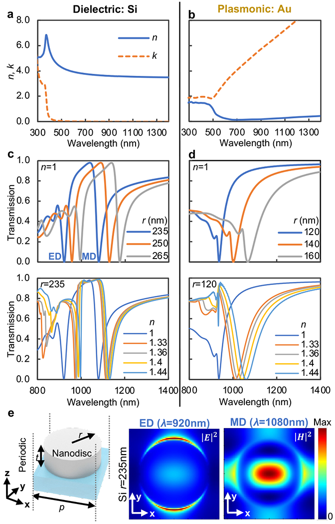
Numerical studies on dielectric (Si) vs. plasmonic (Au) nanodisc metasurfaces. Refractive index of (a) Si (Sik et.al.) and (b) Au (Johnson and Christy). Transmission spectra dependence on nanodisc radius and surrounding medium refractive index for (c) Si and (d) Au metasurfaces. (e) Schematic diagram of the 3D FDTD model (a unit nanodisc with periodic boundary conditions, incident light along z-axis and polarization in y-axis), Si nanodisc x-y cross-sectional electric field and magnetic field intensity distribution at resonance wavelengths.
Table 1.
Si nanodisc array: geometric parameters and sensing performance.
Table 2.
Au nanodisc array: geometric parameters and sensing performance.
Using three-dimensional (3D) Finite-Difference Time-Domain (FDTD) simulations, we investigate closely spaced nanodisc ordered arrays, comparing Si (Fig. 1c) vs. Au (Fig. 1d). The numerical calculations were performed on a single disc unit on glass substrate, with periodic boundary conditions (Fig. 1e). The geometric parameters include the nanodisc radius (r), periodicity (p), and thickness (t). Fig. 1c shows two resonance dips in the transmission spectra of Si nanodisc arrays (r=235nm, p=400nm, t=120nm), representing the electric dipole (ED) and magnetic dipole (MD) at different resonance wavelengths (λr: λ1=920 nm, λ2=1080 nm) respectively. The corresponding electric field and magnetic field distributions in the 2D x-y plane are shown in Fig. 1e. Among the geometric parameters, t is optimized to support resonances with relatively high Q factors; p is optimized to adjust the relative spectral positions between ED and MD; r can be adjusted to tune the spectral positions of the double transmission dips concurrently. The resonances also change with the medium RI, which is used to evaluate the BRIS (148 nm/RIU for the ED resonance, and 96 nm/RIU for the MD resonance). As a direct comparison, the BRIS of Au nanodisc array (r=120nm, p=400nm, t=120nm) is 520 nm/RIU for a similar wavelength range (Fig. 1d).
2.2. Huygens metasurfaces
In order to further improve the sensing performance of Si nanodisc arrays, we need to take a closer look at the physics. In the basic resonance modes, the ED is more sensitive to geometric parameters than MD, so that the relative spectral positions between ED and MD can be tuned. On the one hand, the spectral overlapping of ED and MD provide ideally 100% transmission efficiency and full 2π phase coverage, which is referred to as the Huygens condition [25]. This is the theoretical basis of Huygens metasurfaces, which have been exploited for high-efficiency wavefront engineering, such as meta-lenses [26] and meta-holograms [27]. On the other hand, the mismatch of spectrally adjacent resonances gives rise to a single deep transmission dip, suitable for sensing applications. Following this principle, the geometric parameters can be optimized for higher BRIS (323 nm/RIU at λr=1220 nm) in Si nanodisc arrays [28]. Meanwhile, ultrathin dielectric nanoresonators that are too thin to support Huygens conditions also provide single deep transmission dips [29] and comparable sensing performance (BRIS = 227 nm/RIU at λr=844 nm) [30].
2.3. Sensing parameters
Based on different physical mechanisms, LSPR features strong evanescent fields, while the electromagnetic fields are tightly confined in dielectric meta-atoms (Fig. 1e). This leads to different spatial distribution of enhanced fields in the sensing medium, which is probably why the dielectric metasurface BRIS is generally lower than the plasmonic counterpart (comparing Table 1 and 2). Nevertheless, the evolution of Si nanodisc metasurfaces demonstrates that the BRIS can be improved to a level comparable to that of Au, by optimizing the metasurface geometry and array arrangement (as summarized in Table 1). It should be noted that a higher BRIS does not necessarily correspond to a better limit of detection (LOD), which also depends on many other factors, such as the mode volume and spatial distribution of BRIS [21].
For dielectric metasurfaces, the sensitivity drawback is partially compensated for by lower susceptibility to photothermal heating, and more linear responses to thin layer adsorption [22]. More importantly, dielectric metasurfaces provide smaller resonance bandwidths (Δλ) and higher Q factors (Q=λr/Δλ). The Δλ is usually defined as the full width at half maximum (FWHM), or the spectral distance between the dip and the peak for Fano resonances. High-Q resonances (with small Δλ) provide well-defined signals that are easy-to-track. The figure-of-merit (FOM=BRIS/Δλ, in the unit of RIU−1) considers both sensitivity and resolution in spectral measurement.
Alternatively, for intensity measurement at a fixed wavelength, there is another parameter FOM*=max[(dI/dn)/I] considering the relative intensity change instead of spectral shift [31–33]. In this case, high-Q resonances provide a higher FOM* at the price of a lower dynamic range. Overall, high-Q resonances are preferable for both spectral and intensity measurements, but should be engineered carefully considering the trade-off with other sensing performances. The abovementioned Si Huygens metasurfaces provide a comparable sensitivity and a higher FOM [28] than Au nanodisc arrays [24] (compared in Table 1, 2, and Fig. 2). But limited by the basic circular geometry, the Q factor predicted by standard Mie theory is still relatively low [34]. Low-loss dielectric metasurfaces promise high-Q modes, which have been pursued by exploiting unique physical phenomena based on carefully designed metasurface geometries, as summarized in the following section.
Figure 2.
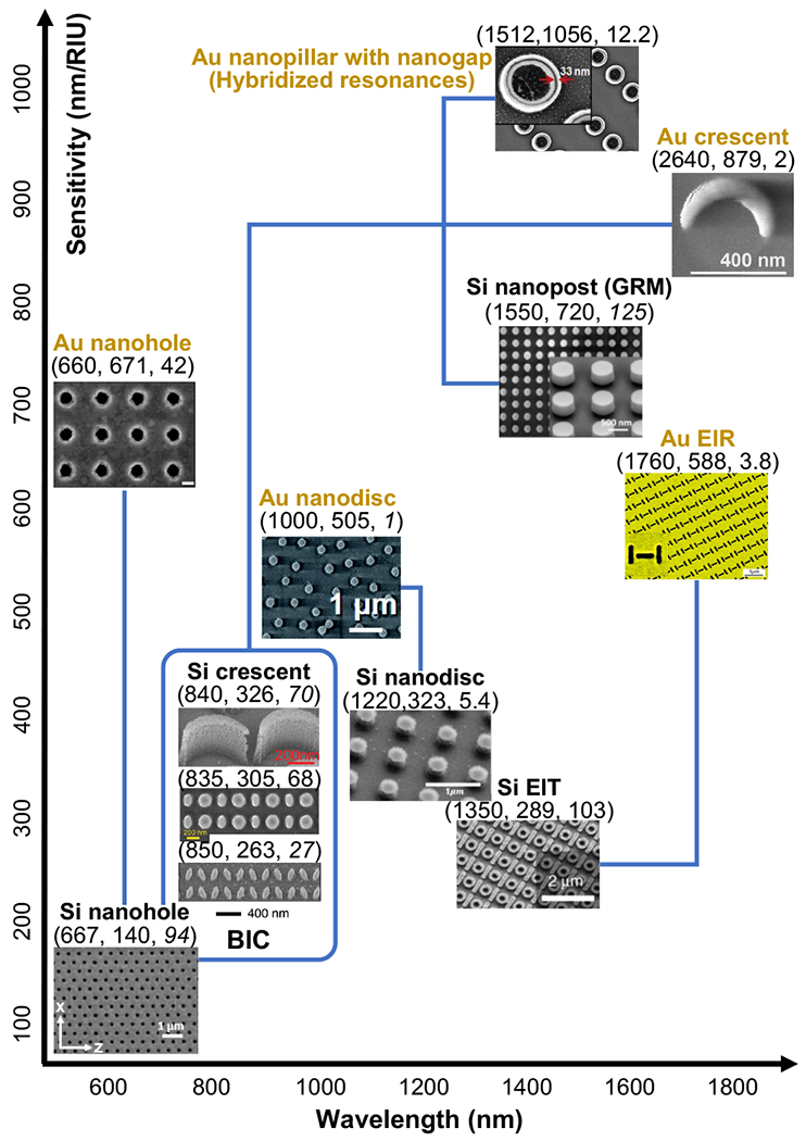
Metasurface with various geometries summarized in a wavelength-sensitivity coordinate plane, comparing Si vs. Au. The coordinates represent (wavelength (nm), sensitivity (nm/RIU), FOM (RIU−1)), Italic fonts indicate approximate estimations based on the data in literature. Nanodisc array: Si [28] John Wiley & Sons. © 2018 Wiley-VCH Verlag GmbH & Co.; vs. Au, reproduced from [24], CC BY 3.0 with permission from the Royal Society of Chemistry. Nanohole array: Si, reproduced from [36], CC BY 4.0; vs. Au, reprinted with permission from [37], Copyright (2015) American Chemical Society. Si EIT, reprinted by permission from [38], Springer Nature, Copyright (2014); vs. Au EIR, reprinted with permission from [39], Copyright (2010) American Chemical Society. Si nanopost with GRM, reprinted from [40], © 2018 Elsevier B.V.; vs. Au nanoplillar with nanogap, reprinted with permission from [41], Copyright (2011) American Chemical Society. Si BIC groups: nanobar zigzag array, reprinted by permission from [43], Springer Nature, Copyright (2019); nanodisc array with ellipticity asymmetry, reproduced from [44], CC BY 4.0; Si nanocrescent array [46], CC BY with the permission from John Wiley & Sons © 2021 Wiley-VCH Verlag GmbH & Co.; vs. Au nanocrescent array, reprinted with permission from [45], Copyright (2010) American Chemical Society.
3. High-Q resonance design
3.1. Fano resonances
Originated from the interference between continuum states and excitation of discrete states, Fano resonance features asymmetric line shapes and strongly dispersive characters, which enable strong line-width narrowing and high Q factors [35]. For example, Si nanohole arrays provide a BRIS of 140 nm/RIU and a high Q of 450 by Fano resonance [36]. A plasmonic version of Au nanohole arrays provide a higher BRIS of 671 nm/RIU at a similar wavelength, but the FOM is lower (nanohole geometry in Fig. 2) [37]. Electromagnetically induced transparency (EIT), another exclusive optical resonance mode arisen from a coherent optical nonlinearity, produces narrow sharp spectral properties. With meta-atoms composed of a ring resonator and a rectangular bar resonator, Si metasurfaces support EIT based on the interference between the collective bright mode (i.e., ED of a bar resonator) and dark mode (i.e., MD of a ring resonator) [38]. The Si EIT metasurfaces provide a high Q of 483 and a FOM of 103 RIU−1, much higher than that of Au EIR (“R” represents reflectance instead of transparency) [39], as shown in Fig. 2.
3.2. Guided and hybridized modes
Even for the basic circular geometry, the sensing performance can be improved by antisymmetric modes at a small oblique angle of incidence. For example, modelling of the Huygens metasurfaces predicts a much higher FOM of 219 at 4° incidence than 5.4 at normal incidence [28]. Si nanoposts with guided mode resonance (GMR) provide a BRIS of 720 nm/RIU and a FOM of ~125 at 1° incidence [40]. In addition to the high FOM, the BRIS also approaches one of the best sensitivity values (1056 nm/RIU) realized by hybridized plasmon resonances supported by Au double nanopillars with nanogaps [41] at a similar wavelength (Fig. 2).
3.3. Bound states in the continuum
Recently, metasurfaces based on the bound states in the continuum (BIC) phenomena have drawn significant attentions, which refer to a completely localized state within a continuous electromagnetic spectrum of the environment [34,42]. Ideally, a true BIC would exhibit an infinite Q factor and vanishing resonance width, which only exist in lossless infinite structures. In practice, BICs can be realized with high but finite Q factors due to structural losses and imperfections, which are termed “quasi-BICs” or “supercavity modes”. Symmetry-breaking strategies have been employed to design diatomic geometries through different controllable variables. For example, at a similar wavelength range around 850 nm, tilted Si nanobars (in a zigzag array) introduce rotation asymmetry, which support a high sensitivity of 263 nm/RIU and a FOM of 27 RIU−1 [43], while nanodiscs with ellipticity asymmetry gives a higher sensitivity of 305 nm/RIU and a FOM of 68 RIU−1 [44]. With a geometry similar to the well-known plasmonic nanocrescent structures [45]. Si crescent metasurfaces provide a slightly higher sensitivity of 326 nm/RIU and a FOM of 70 RIU−1 [46] (BIC group and crescent geometry in Fig. 2). Beyond the mostly used material of Si, BIC is a general phenomenon that can be extended to other dielectric materials like Ge [47], and even plasmonic materials like Au [48].
Interestingly, BIC could also be related to other resonance modes. For example, abovementioned Si nanopost metasurfaces support GMR at oblique incidence and BIC at normal incidence [40]. The transition between Fano and quasi-BIC resonances was demonstrated by simply adjusting the diameter of circular shaped nanoantennas [49]. The BIC concept was also introduced to boost Q factors in Huygens metasurfaces [50]. In the future, besides exploiting new physics and nonlinear optics (e.g., anapoles [51]), it is promising to enable high-Q dielectric metasurfaces by strong mixing of multiple resonances, similar to plasmonics [41]. In practice, the hybridized resonances are difficult to identify, but can be realized by exploring complicated meta-atom geometries. Since computational library search and inverse design strategies [23] have already been successfully developed for meta-optics to achieve high deflection angles [52, 53] or dispersion engineering [54, 55], similar design strategies and tools can be adopted to optimize metasurfaces for sensing applications.
3.4. Array dimension
Due to the strong coupling among dielectric meta-atoms, the array arrangement affects not only BRIS (as shown in Table 1), but also Q factors. Generally, the distance between adjacent meta-atoms is already considered as a geometric factor during meta-atom design. Additionally, it should be noted that the array dimension also plays an important role, which can be underestimated because simulations usually assume an infinite array based on periodic boundary condition (Fig. 1e). In fact, the Q factor increases with increasing array dimension, which was observed in Si EIT metasurfaces [38], and TiO2 metasurfaces developed for photoluminescence control [56]. Therefore, in addition to engineering various resonance modes by the geometric design of single meta-atoms, it is important to take the array arrangement and dimension into consideration. A minimal array dimension is required to support the theoretically predicted high Q factors.
This phenomenon shares similarity with the concept of surface lattice resonance (SLR) in plasmonics, which is based on the diffractive coupling of LSPR nanoparticles in an ordered array. SLRs lead to drastic narrowing of plasmon resonances and high Q factors. Therefore, SLR potentials in biosensing are being explored, among other applications including optoelectronics, photovoltaics, data storage and communications [57]. As a comparison, Au SLR achieved an ultra-high Q factor of 2340 [58], while Si BIC metasurfaces demonstrated a record high Q factor up to 18511 in the same telecommunication wavelength range [59]. It should be pointed out that the ultra-high Q factors achieved by tightly confining electromagnetic fields inside meta-atoms (at a price of lower sensitivity) are more appropriate for nonlinear or lasing applications than biosensing [44].
4. Diverse sensing mechanisms
4.1. Refractometric sensing
As versatile as plasmonic platforms, dielectric metasurfaces support diverse sensing mechanisms. The most basic and straightforward mechanism of refractometric sensing is already discussed in previous sections, i.e., direct detection of RI changes in the surrounding medium, which affect the meta-atom resonances. The RI changes could be either a global change of the bulk medium depending on the analyte and its concentration, or a local environment change due to the deposition of a thin molecular layer on the metasurfaces. The latter is usually implemented by specific biomolecular interactions to ensure the specificity for label-free biosensing.
4.2. Surface-enhanced fluorescence or Raman scattering
Another well studied mechanism is based on the field enhancement by nanoresonators, which can be widely used for surface-enhanced fluorescence (SEF) and surface-enhanced Raman scattering (SERS) spectroscopies. SEF provides strong optical signals that can be directly imaged by fluorescence microscopy, but requires additional processes to attach fluorescence labels to the analytes of interest. Again, take the basic circular geometry as the first example, Iwanaga M et al [60] created Si nanopost arrays on a silicon-on-insulator substrate (Fig. 3a1). The simulated EM-field intensities of |H|2 and |E|2 at the wavelength of 559 nm show approximate 40-fold EM-field intensity enhancements (Fig. 3a2). Since the field enhancement increases with the Q factor [10], metasurfaces with high-Q resonances could provide higher enhancement. Supporting high-Q BICs, Si3N4 nanohole arrays (Fig. 3b1) showed concurrent enhancements of ~103 fold of fluorescence emission (Fig. 3b2) and Raman scattering (Fig. 3b3) far-field intensities of molecules dispersed on these metasurfaces [61]. These results are consistent with previous plasmonic studies, where Au nanohole arrays provided a higher enhancement than nanodisc arrays (Fig. 3f) [62].
Figure 3.
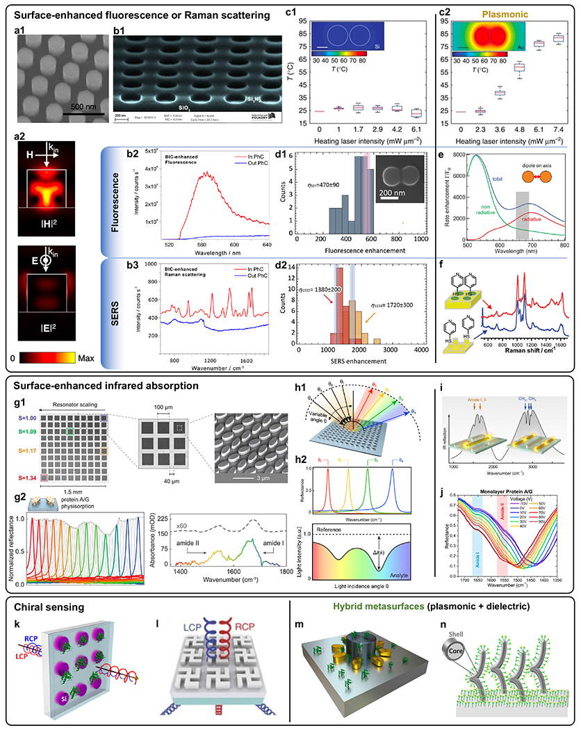
Metasurface sensing mechanisms. I. SEF/SERS. (a) Si nanopost arrays (a1) with simulated EM-field intensities (a2) for SEF detection of protein biomarkers, reproduced from [60] CC BYNC-ND. (b) Si3N4 nanohole arrays (b1) for both SEF (b2, rhodamine-6G) and SERS (b3, crystal violet molecules), reprinted with permission from [61], Copyright (2018) American Chemical Society. (c) Local temperature as a function of laser intensity: Si (c1) vs. Au (c2) dimers, reproduced from [63], CC BY 4.0. (d) Si dimers for both SEF (d1) and SERS (d2) detection of β-carotenal, reprinted with permission from [64], Copyright (2018) American Chemical Society. (e) Self assembled Au nanoparticle dimers for SEF of Alexa Fluor 647, reprinted with permission from [65], Copyright (2015) American Chemical Society. (f) Au nanohole and nanodisc array for SERS detection of 4-mercaptopyridine (4-MP), reprinted with permission from [62], Copyright (2008) American Chemical Society. II. SEIRA. (g) BIC pixelated metasurface (g1) for molecular fingerprinting (g2, protein A/G physisorption) [71], reprinted with permission from AAAS. (h) AFR based on BIC metasurface (h1) for molecular fingerprinting (h2, human ODAM), reproduced from [47], CC BY-NC 4.0. (i) Au multiband IR metasurface for membrane monitoring, reproduced from [69], CC BY 4.0, (j) Tunable graphenemetallic hybrid metasurface for IgG detection reprinted with permission from [70], Copyright (2019) American Chemical Society. III. Chiral sensing. (k) Si metasurface for CD enhancement, reprinted with permission from [72], Copyright (2018) American Chemical Society. (l) TiO2 chiral metasurface, reproduced from [75], CC BY 4.0. (m) Hybrid metallic-dielectric metasurface for CD enhancement, reprinted with permission from [78] https://pubs.acs.org/doi/10.1021/acsphotonics.1c00311 (further permission should be directed to the ACS). (n) Hybrid 3D chiral metamaterial for TDP-43 detection, reprinted with permission from [79], Copyright (2021) American Chemical Society.
We directly compare literatures between Si and Au, based on a typical SEF/SERS metasurface design, where the meta-atoms are dimers of nanodiscs or nanoparticles with a small gap (g) in between, as listed in Table 3 (Fig. 3c–e) [63–65]. At a similar scattering resonance wavelength, Si dimers provide comparable SEF (Fig. 3c1, d1 vs. e1) or lower SERS (Fig. 3c1, d2 vs. c2) enhancement factors. The enhancement can be further increased by reducing the nanogap dimension. As predicted by theoretical simulation, when the Si dimer nanogap reduces from 20 nm to 4 nm, the SERS enhancement factor reaches 106, which could enable in principle single-molecule SERS detection [63, 66]. More importantly, dielectric metasurfaces provide unique advantages over the plasmonic counterparts by eliminating the heating problems. Caldarola M et al [63] studied the local temperature around both Si (Fig. 3c1) and Au (Fig. 3c2) dimers as a function of the heating laser intensity. The measured temperature around the Si dimers remains nearly constant, while that of Au dimers increases by > 60 °C in the given range of laser powers. In plasmonic platforms, SERS is optimized when target molecules are located in the highest field regions, but SEF requires a spacer layer between the fluorophore and nanoantenna to diminish the quenching phenomena. Dielectric metasurfaces overcome this limitation and allow using the same configuration for both SEF and SERS [63].
Table 3.
Surface enhancement by dimer nanoantennas: Si vs. Au.
4.3. Surface-enhanced infrared absorption
Vibrational spectroscopy not only detects the binding of analyte molecules, but also provides specific information of molecular vibrations to identify them (molecular fingerprints). There are two complementary techniques, Raman scattering spectroscopy and infrared (IR) absorption spectroscopy. The former is active for symmetric vibrations that alter the polarizability (bond length), identifying molecular skeletal structures. The latter is active for anti-symmetric vibrations that alter the dipole moment (charge and charge separation), identifying polar bonds in functional groups [67]. Metasurfaces can be used both for SERS and surface-enhanced infrared absorption (SEIRA) spectroscopy, to improve the sensitivity of vibrational spectroscopy. Unlike refractometric sensing and SERS which prefer high Q factors, SEIRA generally requires a wide resonance bandwidth, to cover specific absorption bands distributed in the IR range. In plasmonic SEIRA, the spectral coverage and selectivity have been realized by broadband [68], multiband (Fig. 3i) [69], and active tuning of resonances (Fig. 3j) [70]. Nevertheless, the Altug group recently exploited high-Q BIC dielectric metasurfaces for SEIRA spectroscopy. The unique spectral cleanness and tunability provide unprecedented advantages which cannot be achieved by wide bandwidths of plasmonic antennas. The metasurfaces are composed of multiple pixels, where each “meta-pixel” is a zigzag array of anisotropic Si nanoresonators on MgF2 substate, supporting clean and high-Q (>200) BIC resonances (Fig. 3g1) [71]. The meta-pixels provide not only sharp reflectance resonances, but also straightforward resonance tuning via scaling of the meta-atom geometry, i.e., the resonance spectral position shifts with the scaling factor. The array geometries are systemically changed by the scaling factor, so that the entire spectral working range is covered by the whole pixelated metasurface. This novel platform enables high spectral selectivity and resolution for the enhancement of molecular fingerprint information. Hyperspectral imaging of each meta-pixel measures the analyte-induced intensity reduction of each reflectance peak at a given wavelength. The envelope of all the resonances on the pixelated metasurface reproduces the absorption fingerprint (Fig. 3g2). The results are in good agreement with infrared reflection-absorption spectroscopy (IRRAS). Alternatively, the Altug group also developed a method of angle-multiplexed fingerprint retrieval (AFR) using a single array (Ge nanoresonators on CaF2 substrate, Fig. 3h1) instead of multiple pixels [47]. Based on the bijective relationship between the resonance wavelength and the incidence angle, the angular positions in the measurement of the same array can be associated with different specific target wavelengths in the spectral range. Similarly, analyte-induced light intensity modulation spanning all the incidence angles reproduce the molecular fingerprint (Fig. 3h2). A closer look into the spectra reveals that the majority of the analyte-induced reflectance change occurs only around the resonance peak, which can be approximated by the total reflectance intensity using a broadband light source and detector. Therefore, these methods promise to alleviate the requirement of complex spectroscopic equipment or tunable light sources.
4.4. Chiral sensing
Chirality is a geometric property of objects with non-superimposable mirror images. Chiral biomolecules and drugs have a specific chirality (either left- or right-handed) that determines their physical, chemical properties and biological functions. Circular dichroism (CD) spectroscopy is a unique technology to discriminate chiral molecules by their interactions with circularly polarized light. Dielectric metasurfaces could enhance the CD spectroscopy for chiral molecule detection (Fig. 3k) [72, 73]. Moreover, metasurfaces/metamaterials composed of chiral nanostructures can be used to detect analytes beyond chiral molecules by the CD spectral shift. For example, THz graphene metasurfaces have been used for virus detection using polarization sensitive LSPR [74]. Dielectric chiral metasurfaces significantly improve the CD transmission efficiency (Fig. 3l) [75] than the plasmonic counterparts [76, 77]. Recently, hybrid metasurfaces with combined dielectric and metallic components have been emerging. For example, hybrid nanoresonators provide strong and decoupled electric and magnetic resonances optimized for chiral fields to detect chiral molecules, with 20-fold CD enhancement (Fig. 3m) [78]. In hybrid 3D chiral metamaterials (Fig. 3n) [79], each functional core-shell nanoarchitecture is composed of a plasmonic core and conformal coating of a polymer shell for specific biorecognition. The energy transfer between dielectric shell polarization charges and plasmonic core free electrons provides efficient interactions with biomolecules, enabling femtomolar biodetection. The zero dichroism point (ZDP) spectral shift provides a higher sensitivity and FOM (600, 766, 1276) than the conventional resonance centroid spectral shift, comparing with the (wavelength, sensitivity, FOM) coordinates listed in Fig. 2.
5. Advanced optical readouts
5.1. Intensity readout at a defined wavelength
Conventional refractometric sensing relies on the resonance spectral shift by the measurement of the whole working wavelength range using a spectrometer (Fig. 1c–d). The resonance intensity provides an alternative optical readout at a defined wavelength, which can be quantified by FOM*. Compared with spectral shift (Fig. 4a1), it not only simplifies the optical setup without using spectrometers, but also demonstrates superior performance in some cases, e.g., a lower LOD and a wider dynamic range (Fig. 4a2) [21]. This is in agreement with plasmonic biosensors based on Au nanorods, whose LOD given by scattering intensity is more than 10 times lower than that of spectral shift detection (Fig. 4b) [80].
Figure 4.
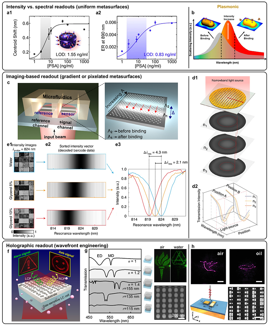
Metasurface optical readouts. I. Comparison between the intensity changes and spectral shifts readouts for (a) dielectric Si nanodisc arrays, reprinted with permission from [21], Copyright (2019) American Chemical Society; and (b) plasmonic Au nanorod arrays, reprinted with permission from [80] Copyright (2015) American Chemical Society. II. Imaging-based readout. (c) Si gradient metasurface of chirped nanohole array, reproduced from [36], CC BY 4.0. (d) Au gradient metasurfaces made by the interference lithography [82], CC BY with the permission from John Wiley & Sons © 2021 Wiley-VCH Verlag GmbH & Co. (e) Algorithm-aided refractometric barcoding based on Si BIC pixelated metasurfaces, reprinted by permission from [43], Springer Nature, Copyright (2019). III. Holographic readout. (f) Polarization-switchable dielectric meta-holograms as gas sensors, reproduced from [84], CC BY-NC 4.0. Medium-switchable meta-holograms with potentials in refractometric sensing applications, comparing (g) dielectric (TiO2), reproduced from [85], Copyright (2021) American Chemical Society; vs. (h) plasmonic (Au) [86], CC BY with the permission from John Wiley & Sons © 2021 Wiley-VCH Verlag GmbH & Co.
5.2. Imaging-based readout on gradient metasurfaces
At a defined wavelength, a single uniform metasurface array provides an intensity readout. Thereby, gradient or pixelated metasurfaces whose geometry is spatially varied could provide an imaging-based optical output, i.e., a pattern of bright/dark bands combining intensity signals across the whole surface. For example, in a chirped configuration of Si nanohole array, the period was varied from 470 nm to 490 nm over a distance of 500 μm, forming a bright band readout at a fixed wavelength of 667nm (Fig. 4c) [36]. The bright band spatially moves as the Fano resonance spectrally shifts during refractometric sensing. The LOD of RI was estimated as 4.6×10⁻⁵ RIU, which is approaching the LOD of 4.6×10⁻⁶ RIU based on a plasmonic version [81]. Notably, based on interference lithography, centimetre-scale Au metasurfaces with a deterministic gradient geometry were conveniently made by the interference between two non-uniform Gaussian-shaped coherent beams. The intensity pattern of a dark ring moves towards the centre when the RI of surrounding medium increases (Fig. 4d1) [82]. In the 3D parameter space of intensity signal, wavelength and geometry (Fig. 4d2), the spatial shift of resonance in the geometric parameter dimension (gradient metasurface) for a given wavelength is an analogue of spectral shift in the wavelength domain for a given geometry (uniform metasurface). Therefore, high-Q resonances supported by dielectric metasurfaces are favourable for both spectral and imaging-based measurements, which potentially provide better imaging quality of the intensity patterns on gradient or pixelated metasurfaces.
In particular, BIC metasurfaces support high-Q resonances whose λr can be easily adjusted by the geometric scaling factor or one of the asymmetry parameters, as summarized in ref [44]. Similar to the SEIRA application but in a different wavelength region, each meta-pixel corresponds to its λr, and the ith meta-pixel corresponds to λr,i, where i=1, 2, …, m, and m is the total number of the meta-pixels. Within a reasonable wavelength range, the spatial shift of intensity pattern over the multi-pixel metasurface at a fixed wavelength λr can be converted to the resonance spectral shift in the adjacent range (λr,1, λr,m). In practice, considering the nanofabrication precision, a limited number of m pixels spanning a small wavelength range are generally too discrete to reconstruct continuous spectra. The Altug group has developed an innovative strategy, which exploits the small deviations of λr caused by nanofabrication imperfection/nonuniformity in each meta-pixel, which are imaged by l×l pixels on the camera, to improve the spectral resolution from m to m×l2 sampling points (Fig. 4e1). In this way, the intensity map over m multi-pixel metasurfaces are refined to m×l2 barcode information, which are further decoded/reordered (Fig. 4e2) to reconstruct the spectra (Fig. 4e3) by post data processing [43]. This algorithm-aided approach creatively reveals robust and ultrasensitive spectral shift from massive (m×l2) image pixels at a single wavelength. It is superior to existing basic intensity or imaging approaches, where substantial information is buried in an ensemble average of discrepant and noisy intensity signals due to the nanofabrication nonuniformity [44]. Comparing the refractometric barcoding with previously discussed SEIRA molecular fingerprinting, both of them are imaging-based and spectrometer-less sensing techniques demonstrated by BIC metasurfaces. Due to the distinct sensing mechanism of SEIRA, meta-pixels of microscale meta-atoms support a series of discrete resonances spanning the Mid-IR spectrum for molecular functional groups of interest, which also requires tunable [71] or broadband [47] light sources. The refractometric barcoding metasurfaces simply work at a single wavelength that is much shorter (near-IR). With smaller meta-atom dimensions (BIC group in Fig. 2), it accommodates massive imaging information for continuous spectral reconstruction, and improves LODs by employing a thresholding method in data processing [43].
5.3. Novel readouts based on wavefront engineering
As abovementioned, metasurface sensors share the same principles with dynamic tunable metasurfaces. Therefore, it is promising to create novel optical readouts by combining the sensing functions with dynamic wavefront engineering. For example, metasurface optical properties [20] and metalens focusing behaviors [83] change with the infiltration medium, such as liquid crystals (LCs). Reversely, the output changes of optical properties (phase, polarization, in addition to intensity) and behaviors (e.g., focusing, beam steering) can be used as readouts for the detection of RI and target analytes. In particular, wavefront engineering opens the door to directly encode information in the output optical signals, e.g., in the form of holograms. Rho et al. integrated holographic metasurface with gas-responsive LCs, so that both gas analyte detection and visual reporting are implemented into a single miniaturized sensor. Upon the target gas absorption, the LC nematic-to-isotropic change converts the polarization state of input light, and thereby switches the optical output of a spin-coded meta-hologram, projecting instantaneous visual alarms (Fig. 4f) [84]. Besides polarization, meta-holograms can also be switched by the simple RI change in the medium (Fig. 4g) [85], which is promising for refractometric sensing. Compared to the plasmonic (Au) version (Fig. 4h) [86]. TiO2 dielectric metasurfaces work with visible light for visual reporting. It even works with unpolarized light, which allows further integration with miniaturized and cost-effective light sources, promising practical ultracompact and wearable applications [84, 85]. The major challenge combining metasurface sensing with wavefront engineering is to develop novel design strategies for improved sensitivity comparable with other types of readout [87].
6. Emerging sensing applications
6.1. Refractometric sensing applications
Dielectric metasurfaces enable planar optics with unprecedented performance, miniaturization, and integrability, paving the way towards ultracompact meta-optical systems for bioimaging applications [88, 89]. Similarly, the unique optical properties and functionalities of dielectric metasurfaces also endow great promise and advantages to replace plasmonic sensors for fast, sensitive, label-free, non-invasive, and real-time detections in every aspect ranging from epidemic disease control to food and environmental hazardous monitoring. In this rapidly growing research field, a wide range of dielectric metasurface-based biosensors have emerged to detect gas molecules, various biomarkers and pathogens. Taking gas sensing as an example, dielectric metasurfaces are not merely an alternative replacement for plasmonic sensors [90], but could enable novel sensing mechanisms and functionalities such as the holographic readouts [84].
Biomolecules:
Specific protein detection via antibody-antigen binding is the most popular biorecognition process. Plasmonic platforms have traditionally been the method of choice for improved performance compared with the commercial standard of protein detection and quantification: Enzyme-Linked Immunosorbent Assay (ELISA, typical LODs of 1pM or less). Recently, Si nanodisc metasurfaces were used to detect prostate-specific antigen (PSA, a biomarker of prostate cancer) with a BRIS of 227 nm/RIU (Table 1) and a LOD of 1.6 ng/mL in human serum [30], comparable to the LOD of 0.87 ng/mL by Au nanorod arrays [91]. Si nanopost metasurfaces with high-Q GMR (as indicated in Fig. 2) were used to detect the epidermal growth factor receptor 2 (ErbB2, a biomarker for early-stage breast cancer screening), with a LOD down to 0.7 ng/mL [40]. More importantly, high-Q resonances supported by dielectric metasurfaces further improve the sensing performance by imaging-based smart data processing. Demonstrated by biotin-streptavidin assays, Si BIC crescent metasurfaces showed a LOD down to nM concentrations with conventional spectral shift [46]. Using the algorithm-aided refractometric barcoding and a pixel-based thresholding method, the LOD of BIC pixelated metasurfaces (Fig. 4e) achieved a record level of less than 3 molecules/μm2 (improved by three orders of magnitude than ensemble averaging) for the most common type of antibody Immunoglobulin G (IgG) [43]. Using IgG detection for a direct comparison, Si gradient nanohole array (Fig. 4c) reached a LOD of ~ 1 pg/mL by imaging-based readouts [36], better than the LOD of sub-1 ng/mL by conventional spectral shift of Au nanohole array [37] or the laboratory standard of 3-5 pg/mL by ELISA. As the performance keeps improving, dielectric metasurfaces will be adopted by broad and practical applications, such as microfluidic-integrated multiplex immunoassays for multiple analytes (e.g., serum cytokines), where plasmonic sensor arrays reached a LOD of 5-20 pg/mL (Fig. 4b). Cytokine quantification provides important clinical information to monitor the immune system status and adjust therapies in various inflammatory disease conditions, including cancer, sepsis, lupus, and graft versus host disease [80].
Extracellular vesicles (EVs):
EVs, also known as exosomes, are another key class of biomarkers in disease diagnostics. EVs are lipid nanovesicles that contain relevant biomolecular information about the parent tumour. Previously, plasmonic biosensors of Au nanohole arrays achieved a LOD to the tune of ~ 3000 CD63-expressing exosomes (670 aM), 104 times higher in sensitivity than that of western blot analysis and 100-fold that of ELISA [92]. Refractometric barcoding based on Si BIC pixelated metasurfaces was capable of real-time monitoring of CD9-expressing EVs at a concentration as low as 200 fM [44]. This demonstrates that the achievable sensitivity for EV detection by dielectric metasurfaces is also getting close to the ELISA level, with the additional unique advantage of imaging-based and spectrometer-less readouts. As EVs usually display more than one protein biomarker on the membrane, signal amplification is possible through secondary labelling with high RI materials such as Au [92] or silica nanoparticles [44].
Pathogens:
Plasmonic biosensors have also been used for pathogens including bacteria [93] and virus [94]. During the recent coronavirus disease 2019 (COVID-19) pandemic, the detection of SARS-CoV-2 virus have been demonstrated by various plasmonic platforms from traditional LSPR [95, 96] to THz toroidal metasurfaces (LOD for spike proteins in the fM level) [97]. The application of dielectric metasurfaces for pathogen or antigen detection is still very much in its nascent stage, but has demonstrated innovative potentials such as the resonance hyperspectral imaging with high spatial resolution (< 1 μm) to resolve single E. coli bacteria [36].
6.2. Surface enhanced spectroscopy applications
Beyond refractometric sensing, dielectric metasurfaces also approach plasmonic performance in surface enhanced spectroscopy, and thereby can be extended to replace plasmonic platforms in those applications. In addition to the early work [61–65] on fluorophore dye molecules and SERS probe molecules, dielectric metasurfaces have been used in practical applications to detect IgG, cancer biomarkers p53 antibody and carcinoembryonic antigen (CEA) [60]. Si nanopost arrays (Fig. 3a) detected IgG by SEF, reaching a LOD on the order of pg/mL or tens of fM, much better than the pM level by ELISA, and close to plasmonic SEF platforms. For example, Au nanoantenna arrays were used to detect Ebola virus antigens with a LOD level of pg/mL [98]. Another plasmonic SEF platform (Au nano-islands on Au film) demonstrated multiplexed detection of 32 protein analytes simultaneously through a microarray scanner with LODs in the fM level [99].
Dielectric metasurface-based SERS and SEIRA molecular fingerprint detections identify and accurately pinpoint the signature of tiny molecules, which is valuable for biochemical sensing and medical diagnostics. After tested by polymer layers such as polymethyl methacrylate (PMMA), metasurface SEIRA fingerprinting has been further extended to biomolecules, such as the detection of protein A/G physisorption (Fig. 3g) [71] and human odontogenic ameloblast-associated protein (ODAM, biomarker for periodontal diseases) by using single-stranded DNA aptamers (Fig. 3h) [47]. As demonstrated by plasmonic metasurfaces, SERS and SEIRA are particularly useful to resolve multianalyte systems, such as monitoring of the dynamic membrane process [69], gas identification [68] and breathalyser for mass screening of COVID-19 [100]. In addition to molecular monolayers (e.g., IgG) [101], SEIRA metasurfaces have also be applied for cell spectroscopy to reveal biological and clinically important information [102].
6.3. Chiral sensing applications
Chirality could be one of the microscopic origins of Alzheimer’s, Parkinson’s, and chronic kidney diseases [78]. Dielectric metasurface enhanced CD spectroscopy can be used for the detection and discrimination of chiral biomolecules and synthesized chiral molecules in drugs, with great potentials in structural biology, chemistry, biomedicine, food and pharmaceutical industries [72, 73, 78]. Furthermore, chiral or polarization sensitive metasurfaces are used for broad targets beyond chiral molecules, from viruses [74] to protein biomarkers, e.g., transactive response DNA-binding protein 43 (TDP-43), a potential biomarker of amyotrophic lateral sclerosis and frontotemporal lobar degeneration, with a LOD down to 10 fM (Fig. 3n) [79].
6.4. Hyperspectral imaging applications
Hyperspectral imaging provides massive information not only for better biomolecular sensing performance than conventional ensemble averaging [43], but also for novel applications to monitor biological entities, such as bacteria mentioned in section 6.1 [36]. In such applications, the unique advantage of minimal heat conversion is even more significant, which allows real-time monitoring of cellular or microbial behaviour in physiological conditions. This can be potentially leveraged for cell biology studies [103], pharmaceutical screening of antibiotics and antivirals [104], on microfluidic evolution chips with multiple downstream interrogations and analyses [105], etc. Interestingly, Si metasurfaces composed of diverse freeform shaped meta-atoms have also been developed for integrated on-chip microspectrometers [106, 107]. Without requirements of convectional spectrometers or tunable light sources, it conveniently works with ordinary LED source and ordinary colour camera, towards hyperspectral imaging with high temporal, spatial and spectral resolution.
7. Discussions and perspectives
Plasmonic sensors have extensively explored various forms from solution-based nanoparticles to surface-based nanostructures, or a combination of both. Instead of dispersed in solution, metasurfaces and metamaterials are nanostructures organized with a long-range order, which are further integrable with photonic circuits, electronics, and microfluidics components. The microfluidic chip-based format allows easy washing steps during analytical procedures, even with complex biological samples in practical applications [79]. Therefore, metasurfaces are suitable for miniaturized lab-on-a-chip devices. With the rapid progress in nanotechnology and metasurfaces, here we discuss important trends in recent and future advances for next-generation optical biosensing.
7.1. Dielectric metasurfaces vs. plasmonic sensors
In the past decades, nanophotonic biosensors have been extended from the extensively studied plasmonic platforms to dielectric metasurfaces, because the latter support high-Q resonances which not only provide better spectral measurement resolution and FOM, but also better FOM* for intensity measurement at a fixed wavelength. More importantly, dielectric metasurfaces solve the plasmonic Ohmic loss and heating problem, thereby enable better repeatability and stability than plasmonic platforms or colloidal nanoparticles for biosensing. On the one hand, high-Q metasurfaces based on various physical phenomena, especially BIC, have been explored for imaging-based and spectrometer-less biosensing, including single-wavelength refractometric barcoding and SEIRA molecular fingerprinting in the respective wavelength regions of interest. Using wavelength-tunable or broadband light sources, hyperspectral imaging provides massive information for smart data processing, enabling better sensing performance than conventional ensemble averaging. On the other hand, using single-wavelength or white light sources, metasurfaces support the engineering of different forms of optical outputs, including direct visual reporting, without any specialized data acquisition and processing. By sidestepping the requirements for sophisticated laboratories, instrument or skilled operators, metasurface-based biosensors enable miniaturization for portable and point-of-care applications, which are important for epidemiological monitoring, and especially suitable for developing countries and resources limited settings.
7.2. Metasurface fabrication and functionalization
Currently, plasmonic biosensors still account for the dominant majority in integrated and multiplexed systems, including lateral flow assays (LFA) [108], microfluidic devices and multiplexed assays [80, 92]. This is attributed partially to the well-established high sensitivity, and partially to the readily available surface biofunctionalization schemes, e.g., thiol chemistry for Au. As the sensing performance keeps improving, the broad adoption of dielectric metasurfaces in practical applications will depend on the technical challenges in fabrication and functionalization.
Compared with plasmonic noble metals, dielectric metasurfaces have lower cost and better compatibility with CMOS nanofabrication processes. Still, current metasurface nanofabrication processes highly rely on e-beam lithography, which comes with high cost and low throughput. In addition to the alternative approaches such as plastic templates [109], interference [82] and nanoimprint lithography [110] developed for plasmonic sensors, dielectric metasurfaces further enable unique fabrication technologies including self-assembly of optical thin glass films [111] and TiO2 nanoparticle-embedded-resin printing [112] for potential scale-up productions. Similarly, 3D metasurfaces and metamaterials are currently limited to low-throughput fabrication processes such as two-photon polymerization [48] and focused ion beam induced deposition [79], while the nano-kirigami technology promises to create controllable 3D nanostructures by 2D patterning and cuts [113, 114]. Since all the biorecognition mechanisms require biomolecular interactions (e.g., antibody-antigen, DNA, aptamers, etc.), metasurface modification is key to ensuring high sensitivity and specificity for diagnostic accuracy. Therefore, particular attention needs to be taken to develop efficient functionalization schemes and reduce non-specific interactions for dielectric metasurfaces.
7.3. Metasurface material and structure design
In this review, most of the biosensing dielectric metasurfaces have been focused on Si for the near-IR and mid-IR spectra. Other dielectric materials, such as Ge for the mid-IR [47] and TiO2 for the visible light [84, 85], have been emerging, while there are still a variety of available materials to be explored depending on the wavelength range. Chalcogenide alloy and glass, such as PbTe [26] and Ge6Se82Te12 [111], are superior materials for IR light, while GaP, GaN are suitable for visible light, as well as diamond and HfO2 for ultraviolet (UV) light [10]. Hybrid metal-dielectric metasurfaces are also used for refractometric [37, 115], surface-enhanced [70] and chiral sensing [78, 79], which not only provide better sensitivity [37] and dynamic tenability [70], but also facilitate the fabrication [48] or functionalization process [79].
The meta-atom design has rapidly evolved, from simple geometries supporting basic resonances to complicated structures with strong mixing of multiple modes, as summarized in Fig. 2. In the future, computational inverse design strategies, such as evolutional [23] or topology optimization [53] and machine learning [116] methods, will produce new meta-atom designs to improve the overall sensing performance and enable novel optical readouts. Meanwhile, oblique incidence angles could also introduce antisymmetric modes [28], and enable the AFR method in SEIRA spectroscopy [47].
New metasurface platforms keep emerging beyond conventional 2D surfaces on rigid and bulky substrates. Conventional substrates break the symmetry of the dielectric environment surrounding meta-atoms, resulting in undesirable side effects including reduced sensitivity and Q factors [117]. In order to improve the sensitivity, 2D meta-atoms can be placed on top of pedestals or pillars which lift the enhanced fields above substrate and promote the overlap with surrounding medium and analytes [38], similar to the plasmonic mushroom structures [118, 119]. Multilayer hybrid systems are also used to engineer the near-field spatial overlap [37, 115]. Furthermore, 3D meta-atom configurations not only promise better sensing performance [48, 120], but could also introduce chirality or polarization sensitivity [79]. Recently, optically “free-floating” metasurfaces have been demonstrated on low-refractive-index Al2O3 membranes, which suppress undesired substrate effects [117]. Finally, soft and flexible substrates will enable conformal and wearable metasurfaces, e.g., attachable to curved goggle or eyewear surfaces, which facilitate visual reporting [84].
Acknowledgements
The authors thank Drs. Daniel Sodickson, Shy Shoham, Mladen Barbic for useful discussions. The authors gratefully acknowledge support from the U.S. National Institute of Biomedical Imaging and Bioengineering (NIBIB), via grant NIH P41EB017183-06S1.
References
- [1].McDonagh C, Burke CS and MacCraith BD 2008. Optical chemical sensors Chem Rev 108 400–22 [DOI] [PubMed] [Google Scholar]
- [2].Altug H, Oh S-H, Maier SA and Homola J 2022. Advances and applications of nanophotonic biosensors Nat Nanotechnol 17 5–16 [DOI] [PubMed] [Google Scholar]
- [3].Anker JN, Hall WP, Lyandres O, Shah NC, Zhao J and Van Duyne R P 2008. Biosensing with plasmonic nanosensors Nat Mater 7 442–53 [DOI] [PubMed] [Google Scholar]
- [4].Schuller JA, Barnard ES, Cai WS, Jun YC, White JS and Brongersma ML 2010. Plasmonics for extreme light concentration and manipulation Nat Mater 9 193–204 [DOI] [PubMed] [Google Scholar]
- [5].Roh S, Chung T and Lee B 2011. Overview of the Characteristics of Micro- and Nano-Structured Surface Plasmon Resonance Sensors Sensors-Basel 11 1565–88 [DOI] [PMC free article] [PubMed] [Google Scholar]
- [6].Chung T, Lee SY, Song EY, Chun H and Lee B 2011. Plasmonic Nanostructures for Nano-Scale Bio-Sensing Sensors-Basel 11 10907–29 [DOI] [PMC free article] [PubMed] [Google Scholar]
- [7].Chung T, Hwang CSH, Ahn MS and Jeong KH 2019. Au/Ag Bimetallic Nanocomposites as a Highly Sensitive Plasmonic Material Plasmonics 14 407–13 [Google Scholar]
- [8].Boriskina SV, Cooper TA, Zeng L, Ni G, Tong JK, Tsurimaki Y, Huang Y, Meroueh L, Mahan G and Chen G 2017. Losses in plasmonics: from mitigating energy dissipation to embracing loss-enabled functionalities Adv Opt Photonics 9 775–827 [Google Scholar]
- [9].Lal S, Clare SE and Halas NJ 2008. Nanoshell-Enabled Photothermal Cancer Therapy: Impending Clinical Impact Accounts of Chemical Research 41 1842–51 [DOI] [PubMed] [Google Scholar]
- [10].Tseng ML, Jahani Y, Leitis A and Altug H 2021. Dielectric Metasurfaces Enabling Advanced Optical Biosensors ACS Photonics 8 47–60 [Google Scholar]
- [11].Raschke G, Brogl S, Susha AS, Rogach AL, Klar TA, Feldmann J, Fieres B, Petkov N, Bein T, Nichtl A and Kürzinger K 2004. Gold Nanoshells Improve Single Nanoparticle Molecular Sensors Nano Lett 4 1853–7 [Google Scholar]
- [12].Peña-Rodríguez O, Caro M, Rivera A, Olivares J, Perlado JM and Caro A 2014. Optical properties of Au-Ag alloys: An ellipsometric study Optical Materials Express 4 403 [Google Scholar]
- [13].Hwang CSH, Ahn M-S and Jeong K-H 2021. Extraordinary sensitivity enhancement of Ag-Au alloy nanohole arrays for label-free detection of Escherichia Coli Biomed Opt Express 12 2734. [DOI] [PMC free article] [PubMed] [Google Scholar]
- [14].Gong C and Leite MS 2016. Noble Metal Alloys for Plasmonics ACS Photonics 3 507–13 [Google Scholar]
- [15].Yu NF and Capasso F 2014. Flat optics with designer metasurfaces Nat Mater 13 139–50 [DOI] [PubMed] [Google Scholar]
- [16].Li NX, Xu ZJ, Dong Y, Hu T, Zhong QZ, Fu YH, Zhu SY and Singh N 2020. Large-area metasurface on CMOS-compatible fabrication platform: driving flat optics from lab to fab Nanophotonics-Berlin 9 3071–87 [Google Scholar]
- [17].Khorasaninejad M, Chen WT, Devlin RC, Oh J, Zhu AY and Capasso F 2016. Metalenses at visible wavelengths: Diffraction-limited focusing and subwavelength resolution imaging Science 352 1190–4 [DOI] [PubMed] [Google Scholar]
- [18].Kuznetsov AI, Miroshnichenko AE, Brongersma ML, Kivshar YS and Luk’yanchuk B 2016. Optically resonant dielectric nanostructures Science 354 2472. [DOI] [PubMed] [Google Scholar]
- [19].Kruk S and Kivshar Y 2017. Functional Meta-Optics and Nanophotonics Govern by Mie Resonances ACS Photonics 4 2638–49 [Google Scholar]
- [20].Dolan JA, Cai H, Delalande L, Li X, Martinson ABF, de Pablo J J, López D and Nealey PF 2021. Broadband Liquid Crystal Tunable Metasurfaces in the Visible: Liquid Crystal Inhomogeneities Across the Metasurface Parameter Space ACS Photonics 8 567–75 [Google Scholar]
- [21].Yavas O, Svedendahl M and Quidant R 2019. Unravelling the Role of Electric and Magnetic Dipoles in Biosensing with Si Nanoresonators ACS Nano 13 4582–8 [DOI] [PubMed] [Google Scholar]
- [22].Bosio N, Sipova-Jungova H, Lank NO, Antosiewicz TJ, Verre R and Kall M 2019. Plasmonic versus All-Dielectric Nanoantennas for Refractometric Sensing: A Direct Comparison ACS Photonics 6 1556–64 [Google Scholar]
- [23].Cai H, Srinivasan S, Czaplewski DA, Martinson ABF, Gosztola DJ, Stan L, Loeffler T, Sankaranarayanan SKRS and López D 2020. Inverse design of metasurfaces with non-local interactions npj Computational Materials 6 1–8 [Google Scholar]
- [24].Michieli N, Balasa IG, Kalinic B, Cesca T and Mattei G 2020. Optimal geometry for plasmonic sensing with non-interacting Au nanodisk arrays Nanoscale Advances 2 3304–15 [DOI] [PMC free article] [PubMed] [Google Scholar]
- [25].Decker M, Staude I, Falkner M, Dominguez J, Neshev DN, Brener I, Pertsch T and Kivshar YS 2015. High-Efficiency Dielectric Huygens’ Surfaces Adv Opt Mater 3 813–20 [Google Scholar]
- [26].Zhang L, Ding J, Zheng H, An S, Lin H, Zheng B, Du Q, Yin G, Michon J, Zhang Y, Fang Z, Shalaginov MY, Deng L, Gu T, Zhang H and Hu J 2018. Ultra-thin high-efficiency mid-infrared transmissive Huygens meta-optics Nat Commun 9 1481. [DOI] [PMC free article] [PubMed] [Google Scholar]
- [27].Chong KE, Wang L, Staude I, James AR, Dominguez J, Liu S, Subramania GS, Decker M, Neshev DN, Brener I and Kivshar YS 2016. Efficient Polarization-Insensitive Complex Wavefront Control Using Huygens’ Metasurfaces Based on Dielectric Resonant Meta-atoms ACS Photonics 3 514–9 [Google Scholar]
- [28].Ollanik AJ, Oguntoye IO, Hartfield GZ and Escarra MD 2018. Highly Sensitive, Affordable, and Adaptable Refractive Index Sensing with Silicon-Based Dielectric Metasurfaces Adv Mater Technol-Us 4 1800567 [Google Scholar]
- [29].Cai H, Czaplewski D, Ogando K, Martinson A, Gosztola D, Stan L and López D 2019. Ultrathin transmissive metasurfaces for multi-wavelength optics in the visible Appl Phys Lett 114 071106 [Google Scholar]
- [30].Yavas O, Svedendahl M, Dobosz P, Sanz V and Quidant R 2017. On-a-chip Biosensing Based on All-Dielectric Nanoresonators Nano Lett 17 4421–6 [DOI] [PubMed] [Google Scholar]
- [31].Becker J, Trügler A, Jakab A, Hohenester U and Sönnichsen C 2010. The Optimal Aspect Ratio of Gold Nanorods for Plasmonic Bio-sensing Plasmonics 5 161–7 [Google Scholar]
- [32].Liu N, Mesch M, Weiss T, Hentschel M and Giessen H 2010. Infrared Perfect Absorber and Its Application As Plasmonic Sensor Nano Lett 10 2342–8 [DOI] [PubMed] [Google Scholar]
- [33].Wu PC, Liao CY, Chen J-W and Tsai DP 2017. Isotropic Absorption and Sensor of Vertical Split-Ring Resonator Adv Opt Mater 5 1600581 [Google Scholar]
- [34].Rybin MV, Koshelev KL, Sadrieva ZF, Samusev KB, Bogdanov AA, Limonov MF and Kivshar YS 2017. High-Q Supercavity Modes in Subwavelength Dielectric Resonators Phys Rev Lett 119 243901. [DOI] [PubMed] [Google Scholar]
- [35].Yanik AA, Cetin AE, Huang M, Artar A, Mousavi SH, Khanikaev A, Connor JH, Shvets G and Altug H 2011. Seeing protein monolayers with naked eye through plasmonic Fano resonances P Natl Acad Sci USA 108 11784–9 [DOI] [PMC free article] [PubMed] [Google Scholar]
- [36].Conteduca D, Barth I, Pitruzzello G, Reardon CP, Martins ER and Krauss TF 2021. Dielectric nanohole array metasurface for high-resolution near-field sensing and imaging Nat Commun 12 3293. [DOI] [PMC free article] [PubMed] [Google Scholar]
- [37].Cetin AE, Etezadi D, Galarreta BC, Busson MP, Eksioglu Y and Altug H 2015. Plasmonic Nanohole Arrays on a Robust Hybrid Substrate for Highly Sensitive Label-Free Biosensing ACS Photonics 2 1167–74 [Google Scholar]
- [38].Yang Y, Kravchenko II, Briggs DP and Valentine J 2014. All-dielectric metasurface analogue of electromagnetically induced transparency Nat Commun 5 5753. [DOI] [PubMed] [Google Scholar]
- [39].Liu N, Weiss T, Mesch M, Langguth L, Eigenthaler U, Hirscher M, Sönnichsen C and Giessen H 2010. Planar Metamaterial Analogue of Electromagnetically Induced Transparency for Plasmonic Sensing Nano Lett 10 1103–7 [DOI] [PubMed] [Google Scholar]
- [40].Wang Y, Ali MA, Chow EKC, Dong L and Lu M 2018. An optofluidic metasurface for lateral flow-through detection of breast cancer biomarker Biosensors and Bioelectronics 107 224–9 [DOI] [PubMed] [Google Scholar]
- [41].Kubo W and Fujikawa S 2011. Au Double Nanopillars with Nanogap for Plasmonic Sensor Nano Lett 11 8–15 [DOI] [PubMed] [Google Scholar]
- [42].Koshelev K, Lepeshov S, Liu M, Bogdanov A and Kivshar Y 2018. Asymmetric Metasurfaces with High-Q Resonances Governed by Bound States in the Continuum Phys Rev Lett 121 193903. [DOI] [PubMed] [Google Scholar]
- [43].Yesilkoy F, Arvelo ER, Jahani Y, Liu M, Tittl A, Cevher V, Kivshar Y and Altug H 2019. Ultrasensitive hyperspectral imaging and biodetection enabled by dielectric metasurfaces Nat Photonics 13 390–6 [Google Scholar]
- [44].Jahani Y, Arvelo ER, Yesilkoy F, Koshelev K, Cianciaruso C, De Palma M, Kivshar Y and Altug H 2021. Imaging-based spectrometer-less optofluidic biosensors based on dielectric metasurfaces for detecting extracellular vesicles Nat Commun 12 3246. [DOI] [PMC free article] [PubMed] [Google Scholar]
- [45].Bukasov R, Ali TA, Nordlander P and Shumaker-Parry JS 2010. Probing the Plasmonic Near-Field of Gold Nanocrescent Antennas ACS Nano 4 6639–50 [DOI] [PubMed] [Google Scholar]
- [46].Wang J, Kühne J, Karamanos T, Rockstuhl C, Maier SA and Tittl A 2021. All-Dielectric Crescent Metasurface Sensor Driven by Bound States in the Continuum Adv Funct Mater 31 2104652 [Google Scholar]
- [47].Leitis A, Tittl A, Liu M, Lee BH, Gu MB, Kivshar YS and Altug H 2019. Angle-multiplexed all-dielectric metasurfaces for broadband molecular fingerprint retrieval Science Advances 5 eaaw2871. [DOI] [PMC free article] [PubMed] [Google Scholar]
- [48].Liang Y, Koshelev K, Zhang F, Lin H, Lin S, Wu J, Jia B and Kivshar Y 2020. Bound States in the Continuum in Anisotropic Plasmonic Metasurfaces Nano Lett 20 6351–6 [DOI] [PubMed] [Google Scholar]
- [49].Melik-Gaykazyan E, Koshelev K, Choi J-H, Kruk SS, Bogdanov A, Park H-G and Kivshar Y 2021. From Fano to Quasi-BIC Resonances in Individual Dielectric Nanoantennas Nano Lett 21 1765–71 [DOI] [PubMed] [Google Scholar]
- [50].Liu MK and Choi DY 2018. Extreme Huygens’ Metasurfaces Based on Quasi-Bound States in the Continuum Nano Lett 18 8062–9 [DOI] [PubMed] [Google Scholar]
- [51].Semmlinger M, Zhang M, Tseng ML, Huang T-T, Yang J, Tsai DP, Nordlander P and Halas NJ 2019. Generating Third Harmonic Vacuum Ultraviolet Light with a TiO2 Metasurface Nano Lett 19 8972–8 [DOI] [PubMed] [Google Scholar]
- [52].Khaidarov E, Hao HF, Paniagua-Dominguez R, Yu YF, Fu YH, Valuckas V, Yap SLK, Toh YT, Ng JSK and Kuznetsov AI 2017. Asymmetric Nanoantennas for Ultrahigh Angle Broadband Visible Light Bending Nano Lett 17 6267–72 [DOI] [PubMed] [Google Scholar]
- [53].Sell D, Yang JJ, Doshay S, Yang R and Fan JA 2017. Large-Angle, Multifunctional Metagratings Based on Freeform Multimode Geometries Nano Lett 17 3752–7 [DOI] [PubMed] [Google Scholar]
- [54].Chen WT, Zhu AY, Sanjeev V, Khorasaninejad M, Shi Z, Lee E and Capasso F 2018. A broadband achromatic metalens for focusing and imaging in the visible Nat Nanotechnol 13 220–6 [DOI] [PubMed] [Google Scholar]
- [55].Shrestha S, Overvig AC, Lu M, Stein A and Yu N 2018. Broadband achromatic dielectric metalenses Light Sci Appl 7 85. [DOI] [PMC free article] [PubMed] [Google Scholar]
- [56].Lin Y-T, Hassanfiroozi A, Jiang W-R, Liao M-Y, Lee W-J and Wu PC 2022. Photoluminescence enhancement with all-dielectric coherent metasurfaces Nanophotonics-Berlin 11 2701–9 [Google Scholar]
- [57].Kravets VG, Kabashin AV, Barnes WL and Grigorenko AN 2018. Plasmonic Surface Lattice Resonances: A Review of Properties and Applications Chemical Reviews 118 5912–51 [DOI] [PMC free article] [PubMed] [Google Scholar]
- [58].Bin-Alam MS, Reshef O, Mamchur Y, Alam MZ, Carlow G, Upham J, Sullivan BT, Menard JM, Huttunen MJ, Boyd RW and Dolgaleva K 2021. Ultra-high-Q resonances in plasmonic metasurfaces Nat Commun 12 974. [DOI] [PMC free article] [PubMed] [Google Scholar]
- [59].Liu Z, Xu Y, Lin Y, Xiang J, Feng T, Cao Q, Li J, Lan S and Liu J 2019. High-Q Quasibound States in the Continuum for Nonlinear Metasurfaces Phys Rev Lett 123 253901. [DOI] [PubMed] [Google Scholar]
- [60].Iwanaga M 2020. All-Dielectric Metasurface Fluorescence Biosensors for High-Sensitivity Antibody/Antigen Detection ACS Nano 14 17458–67 [DOI] [PubMed] [Google Scholar]
- [61].Romano S, Zito G, Managó S, Calafiore G, Penzo E, Cabrini S, De Luca AC and Mocella V 2018. Surface-Enhanced Raman and Fluorescence Spectroscopy with an All-Dielectric Metasurface The Journal of Physical Chemistry C 122 19738–45 [Google Scholar]
- [62].Yu Q, Guan P, Qin D, Golden G and Wallace PM 2008. Inverted Size-Dependence of Surface-Enhanced Raman Scattering on Gold Nanohole and Nanodisk Arrays Nano Lett 8 1923–8 [DOI] [PubMed] [Google Scholar]
- [63].Caldarola M, Albella P, Cortés E, Rahmani M, Roschuk T, Grinblat G, Oulton RF, Bragas AV and Maier SA 2015. Non-plasmonic nanoantennas for surface enhanced spectroscopies with ultra-low heat conversion Nat Commun 6 7915. [DOI] [PMC free article] [PubMed] [Google Scholar]
- [64].Cambiasso J, König M, Cortés E, Schlucker S and Maier SA 2018. Surface-Enhanced Spectroscopies of a Molecular Monolayer in an All-Dielectric Nanoantenna ACS Photonics 5 1546–57 [Google Scholar]
- [65].Punj D, Regmi R, Devilez A, Plauchu R, Moparthi SB, Stout B, Bonod N, Rigneault H and Wenger J 2015. Self-Assembled Nanoparticle Dimer Antennas for Plasmonic-Enhanced Single-Molecule Fluorescence Detection at Micromolar Concentrations ACS Photonics 2 1099–107 [Google Scholar]
- [66].Albella P, Poyli MA, Schmidt MK, Maier SA, Moreno F, Saenz JJ and Aizpurua J 2013. Low-Loss Electric and Magnetic Field-Enhanced Spectroscopy with Subwavelength Silicon Dimers J Phys Chem C 117 13573–84 [Google Scholar]
- [67].Larkin PJ. Infrared and Raman Spectroscopy: Principles and Spectral Interpretation 2011 [Google Scholar]
- [68].Hu H, Yang X, Guo X, Khaliji K, Biswas SR, Garcia de Abajo FJ, Low T, Sun Z and Dai Q 2019. Gas identification with graphene plasmons Nat Commun 10 1131. [DOI] [PMC free article] [PubMed] [Google Scholar]
- [69].Rodrigo D, Tittl A, Ait-Bouziad N, John-Herpin A, Limaj O, Kelly C, Yoo D, Wittenberg NJ, Oh SH, Lashuel HA and Altug H 2018. Resolving moleculespecific information in dynamic lipid membrane processes with multi-resonant infrared metasurfaces Nat Commun 9 2160. [DOI] [PMC free article] [PubMed] [Google Scholar]
- [70].Li ZY, Zhu YB, Hao YF, Gao M, Lu M, Stein A, Park AHA, Hone JC, Lin Q and Yu NF 2019. Hybrid Metasurface-Based Mid-Infrared Biosensor for Simultaneous Quantification and Identification of Monolayer Protein ACS Photonics 6 501–9 [Google Scholar]
- [71].Tittl A, Leitis A, Liu M, Yesilkoy F, Choi DY, Neshev DN, Kivshar YS and Altug H 2018. Imaging-based molecular barcoding with pixelated dielectric metasurfaces Science 360 1105–9 [DOI] [PubMed] [Google Scholar]
- [72].Mohammadi E, Tsakmakidis KL, Askarpour AN, Dehkhoda P, Tavakoli A and Altug H 2018. Nanophotonic Platforms for Enhanced Chiral Sensing ACS Photonics 5 2669–75 [Google Scholar]
- [73].Mohammadi E, Tavakoli A, Dehkhoda P, Jahani Y, Tsakmakidis KL, Tittl A and Altug H 2019. Accessible Superchiral Near-Fields Driven by Tailored Electric and Magnetic Resonances in All-Dielectric Nanostructures ACS Photonics 6 1939–46 [Google Scholar]
- [74].Amin M, Siddiqui O, Abutarboush H, Farhat M and Ramzan R 2021. A THz graphene metasurface for polarization selective virus sensing Carbon N Y 176 580–91 [DOI] [PMC free article] [PubMed] [Google Scholar]
- [75].Zhu AY, Chen WT, Zaidi A, Huang YW, Khorasaninejad M, Sanjeev V, Qiu CW and Capasso F 2018. Giant intrinsic chiro-optical activity in planar dielectric nanostructures Light Sci Appl 7 17158. [DOI] [PMC free article] [PubMed] [Google Scholar]
- [76].Hentschel M, Schaferling M, Duan X, Giessen H and Liu N 2017. Chiral plasmonics Sci Adv 3 e1602735. [DOI] [PMC free article] [PubMed] [Google Scholar]
- [77].Collins JT, Kuppe C, Hooper DC, Sibilia C, Centini M and Valev VK 2017. Chirality and Chiroptical Effects in Metal Nanostructures: Fundamentals and Current Trends Adv Opt Mater 5 [Google Scholar]
- [78].Mohammadi E, Tittl A, Tsakmakidis KL, Raziman TV and Curto AG 2021. Dual Nanoresonators for Ultrasensitive Chiral Detection ACS Photonics 8 1754–62 [DOI] [PMC free article] [PubMed] [Google Scholar]
- [79].Manoccio M, Esposito M, Primiceri E, Leo A, Tasco V, Cuscuna M, Zuev D, Sun Y, Maruccio G, Romano A, Quattrini A, Gigli G and Passaseo A 2021. Femtomolar Biodetection by a Compact Core-Shell 3D Chiral Metamaterial Nano Lett 21 6179–87 [DOI] [PubMed] [Google Scholar]
- [80].Chen P, Chung MT, McHugh W, Nidetz R, Li Y, Fu J, Cornell TT, Shanley TP and Kurabayashi K 2015. Multiplex Serum Cytokine Immunoassay Using Nanoplasmonic Biosensor Microarrays ACS Nano 9 4173–81 [DOI] [PMC free article] [PubMed] [Google Scholar]
- [81].Blanchard-Dionne A-P and Meunier M 2018. Multiperiodic nanohole array for high precision sensing Nanophotonics-Berlin 8 325–9 [Google Scholar]
- [82].Min S, Li S, Zhu Z, Liu Y, Liang C, Cai J, Han F, Li Y, Cai W, Cheng X and Li WD 2021. Ultrasensitive Molecular Detection by Imaging of Centimeter-Scale Metasurfaces with a Deterministic Gradient Geometry Adv Mater 33 e2100270. [DOI] [PubMed] [Google Scholar]
- [83].Lininger A, Zhu AY, Park JS, Palermo G, Chatterjee S, Boyd J, Capasso F and Strangi G 2020. Optical properties of metasurfaces infiltrated with liquid crystals Proc Natl Acad Sci U S A 117 20390–6 [DOI] [PMC free article] [PubMed] [Google Scholar]
- [84].Kim I, Kim W-S, Kim K, Ansari MA, Mehmood MQ, Badloe T, Kim Y, Gwak J, Lee H, Kim Y-K and Rho J 2021. Holographic metasurface gas sensors for instantaneous visual alarms Science Advances 7 eabe9943. [DOI] [PMC free article] [PubMed] [Google Scholar]
- [85].Cai H, Dolan JA, Gordon GSD, Chung T and López D 2021. Polarization-Insensitive Medium-Switchable Holographic Metasurfaces ACS Photonics 8 2581–9 [Google Scholar]
- [86].Xiong B, Xu Y, Wang J, Li L, Deng L, Cheng F, Peng RW, Wang M and Liu Y 2021. Realizing Colorful Holographic Mimicry by Metasurfaces Adv Mater 33 2005864. [DOI] [PubMed] [Google Scholar]
- [87].Lee Y, Kim SJ, Park H and Lee B 2017. Metamaterials and Metasurfaces for Sensor Applications Sensors (Basel) 17 1–28 [DOI] [PMC free article] [PubMed] [Google Scholar]
- [88].Pahlevaninezhad H, Khorasaninejad M, Huang YW, Shi Z, Hariri LP, Adams DC, Ding V, Zhu A, Qiu CW, Capasso F and Suter MJ 2018. Nano-optic endoscope for high-resolution optical coherence tomography in vivo Nat Photonics 12 540–7 [DOI] [PMC free article] [PubMed] [Google Scholar]
- [89].Pahlevaninezhad M, Huang YW, Pahlevani M, Bouma B, Suter MJ, Capasso F and Pahlevaninezhad H 2022. Metasurface-based bijective illumination collection imaging provides high-resolution tomography in three dimensions Nat Photonics 16 203–11 [DOI] [PMC free article] [PubMed] [Google Scholar]
- [90].Bingham JM, Anker JN, Kreno LE and Van Duyne R P 2010. Gas Sensing with High-Resolution Localized Surface Plasmon Resonance Spectroscopy J Am Chem Soc 132 17358–9 [DOI] [PMC free article] [PubMed] [Google Scholar]
- [91].Aćimović SS, Ortega MA, Sanz V, Berthelot J, Garcia-Cordero JL, Renger J, Maerkl SJ, Kreuzer MP and Quidant R 2014. LSPR Chip for Parallel, Rapid, and Sensitive Detection of Cancer Markers in Serum Nano Lett 14 2636–41 [DOI] [PubMed] [Google Scholar]
- [92].Im H, Shao H, Park YI, Peterson VM, Castro CM, Weissleder R and Lee H 2014. Label-free detection and molecular profiling of exosomes with a nanoplasmonic sensor Nature Biotechnology 32 490–5 [DOI] [PMC free article] [PubMed] [Google Scholar]
- [93].Gomez-Cruz J, Nair S, Manjarrez-Hernandez A, Gavilanes-Parra S, Ascanio G and Escobedo C 2018. Cost-effective flow-through nanohole array-based biosensing platform for the label-free detection of uropathogenic E. coli in real time Biosensors & Bioelectronics 106 105–10 [DOI] [PubMed] [Google Scholar]
- [94].Yanik AA, Huang M, Kamohara O, Artar A, Geisbert TW, Connor JH and Altug H 2010. An Optofluidic Nanoplasmonic Biosensor for Direct Detection of Live Viruses from Biological Media Nano Lett 10 4962–9 [DOI] [PMC free article] [PubMed] [Google Scholar]
- [95].Qiu G, Gai Z, Tao Y, Schmitt J, Kullak-Ublick GA and Wang J 2020. Dual-Functional Plasmonic Photothermal Biosensors for Highly Accurate Severe Acute Respiratory Syndrome Coronavirus 2 Detection ACS Nano 14 5268–77 [DOI] [PubMed] [Google Scholar]
- [96].Yang Y, Murray J, Haverstick J, Tripp RA and Zhao Y 2022. Silver nanotriangle array based LSPR sensor for rapid coronavirus detection Sens Actuators B Chem 359 131604. [DOI] [PMC free article] [PubMed] [Google Scholar]
- [97].Ahmadivand A, Gerislioglu B, Ramezani Z, Kaushik A, Manickam P and Ghoreishi SA 2021. Functionalized terahertz plasmonic metasensors: Femtomolar-level detection of SARS-CoV-2 spike proteins Biosensors and Bioelectronics 177 112971. [DOI] [PMC free article] [PubMed] [Google Scholar]
- [98].Zang F, Su Z, Zhou L, Konduru K, Kaplan G and Chou SY 2019. Ultrasensitive Ebola Virus Antigen Sensing via 3D Nanoantenna Arrays Adv Mater 31 e1902331. [DOI] [PubMed] [Google Scholar]
- [99].Tabakman SM, Lau L, Robinson JT, Price J, Sherlock SP, Wang H, Zhang B, Chen Z, Tangsombatvisit S, Jarrell JA, Utz PJ and Dai H 2011. Plasmonic substrates for multiplexed protein microarrays with femtomolar sensitivity and broad dynamic range Nat Commun 2 466. [DOI] [PMC free article] [PubMed] [Google Scholar]
- [100].Leong SX, Leong YX, Tan EX, Sim HYF, Koh CSL, Lee YH, Chong C, Ng LS, Chen JRT, Pang DWC, Nguyen LBT, Boong SK, Han X, Kao YC, Chua YH, Phan-Quang GC, Phang IY, Lee HK, Abdad MY, Tan NS and Ling XY 2022. Noninvasive and Point-of-Care Surface-Enhanced Raman Scattering (SERS)-Based Breathalyzer for Mass Screening of Coronavirus Disease 2019 (COVID-19) under 5 min ACS Nano 16 2629–39 [DOI] [PubMed] [Google Scholar]
- [101].Wu C, Khanikaev AB, Adato R, Arju N, Yanik AA, Altug H and Shvets G 2012. Fano-resonant asymmetric metamaterials for ultrasensitive spectroscopy and identification of molecular monolayers Nat Mater 11 69–75 [DOI] [PubMed] [Google Scholar]
- [102].Kelp G, Arju N, Lee A, Esquivel E, Delgado R, Yu Y, Dutta-Gupta S, Sokolov K and Shvets G 2019. Application of metasurface-enhanced infra-red spectroscopy to distinguish between normal and cancerous cell types The Analyst 144 1115–27 [DOI] [PMC free article] [PubMed] [Google Scholar]
- [103].Huang SH, Li J, Fan Z, Delgado R and Shvets G 2021. Monitoring the effects of chemical stimuli on live cells with metasurface-enhanced infrared reflection spectroscopy Lab Chip 21 3991–4004 [DOI] [PMC free article] [PubMed] [Google Scholar]
- [104].Ho CS, Jean N, Hogan CA, Blackmon L, Jeffrey SS, Holodniy M, Banaei N, Saleh AAE, Ermon S and Dionne J 2019. Rapid identification of pathogenic bacteria using Raman spectroscopy and deep learning Nat Commun 10 4927. [DOI] [PMC free article] [PubMed] [Google Scholar]
- [105].Yeh Y-T, Gulino K, Zhang Y, Sabestien A, Chou T-W, Zhou B, Lin Z, Albert I, Lu H, Swaminathan V, Ghedin E and Terrones M 2020. A rapid and label-free platform for virus capture and identification from clinical samples Proceedings of the National Academy of Sciences 117 895–901 [DOI] [PMC free article] [PubMed] [Google Scholar]
- [106].Yang J, Cui K, Cai X, Xiong J, Zhu H, Rao S, Xu S, Huang Y, Liu F, Feng X and Zhang W 2022. Ultraspectral Imaging Based on Metasurfaces with Freeform Shaped Meta-Atoms Laser Photonics Rev 16 2100663 [Google Scholar]
- [107].Xiong J, Cai X, Cui K, Huang Y, Yang J, Zhu H, Li W, Hong B, Rao S, Zheng Z, Xu S, He Y, Liu F, Feng X and Zhang W 2022. Dynamic brain spectrum acquired by a real-time ultraspectral imaging chip with reconfigurable metasurfaces Optica 9 461 [Google Scholar]
- [108].De Puig H, Bosch I, Gehrke L and Hamad-Schifferli K 2017. Challenges of the Nano-Bio Interface in Lateral Flow and Dipstick Immunoassays Trends in Biotechnology 35 1169–80 [DOI] [PMC free article] [PubMed] [Google Scholar]
- [109].Ahmed R, Ozen MO, Karaaslan MG, Prator CA, Thanh C, Kumar S, Torres L, Iyer N, Munter S, Southern S, Henrich TJ, Inci F and Demirci U 2020. Tunable Fano-Resonant Metasurfaces on a Disposable Plastic-Template for Multimodal and Multiplex Biosensing Adv Mater 32 e1907160. [DOI] [PMC free article] [PubMed] [Google Scholar]
- [110].Lee S-W, Lee K-S, Ahn J, Lee J-J, Kim M-G and Shin Y-B 2011. Highly Sensitive Biosensing Using Arrays of Plasmonic Au Nanodisks Realized by Nanoimprint Lithography ACS Nano 5 897–904 [DOI] [PubMed] [Google Scholar]
- [111].Das Gupta T, Martin-Monier L, Yan W, Le Bris A, Nguyen-Dang T, Page AG, Ho KT, Yesilkoy F, Altug H, Qu Y and Sorin F 2019. Self-assembly of nanostructured glass metasurfaces via templated fluid instabilities Nat Nanotechnol 14 320–7 [DOI] [PubMed] [Google Scholar]
- [112].Yoon G, Kim K, Huh D, Lee H and Rho J 2020. Single-step manufacturing of hierarchical dielectric metalens in the visible Nat Commun 11 2268. [DOI] [PMC free article] [PubMed] [Google Scholar]
- [113].Zhang X, Medina L, Cai H, Aksyuk V, Espinosa HD and Lopez D 2021. Kirigami Engineering— Nanoscale Structures Exhibiting a Range of Controllable 3D Configurations Adv Mater 33 2005275. [DOI] [PubMed] [Google Scholar]
- [114].Liu Z, Du H, Li J, Lu L, Li ZY and Fang NX 2018. Nano-kirigami with giant optical chirality Sci Adv 4 eaat4436. [DOI] [PMC free article] [PubMed] [Google Scholar]
- [115].Ray D, Raziman TV, Santschi C, Etezadi D, Altug H and Martin OJF 2020. Hybrid Metal-Dielectric Metasurfaces for Refractive Index Sensing Nano Lett 20 8752–9 [DOI] [PubMed] [Google Scholar]
- [116].Jiang J and Fan JA 2019. Global Optimization of Dielectric Metasurfaces Using a Physics-Driven Neural Network Nano Lett 19 5366–72 [DOI] [PubMed] [Google Scholar]
- [117].Leitis A, Tseng ML, John-Herpin A, Kivshar YS and Altug H 2021. Wafer-Scale Functional Metasurfaces for Mid-Infrared Photonics and Biosensing Adv Mater 33 2102232. [DOI] [PMC free article] [PubMed] [Google Scholar]
- [118].Shen Y, Zhou J, Liu T, Tao Y, Jiang R, Liu M, Xiao G, Zhu J, Zhou ZK, Wang X, Jin C and Wang J 2013. Plasmonic gold mushroom arrays with refractive index sensing figures of merit approaching the theoretical limit Nat Commun 4 2381. [DOI] [PubMed] [Google Scholar]
- [119].Dmitriev A, Hägglund C, Chen S, Fredriksson H, Pakizeh T, Käll M and Sutherland DS 2008. Enhanced Nanoplasmonic Optical Sensors with Reduced Substrate Effect Nano Lett 8 3893–8 [DOI] [PubMed] [Google Scholar]
- [120].Wu PC, Sun G, Chen WT, Yang K-Y, Huang Y-W, Chen Y-H, Huang HL, Hsu W-L, Chiang HP and Tsai DP 2014. Vertical split-ring resonator based nanoplasmonic sensor Appl Phys Lett 105 033105 [Google Scholar]