

Abstract

The growth of transition-metal dichalcogenides (TMDCs) has been performed so far using most established thin-film growth techniques (e.g., vapor phase transport, chemical vapor deposition, molecular beam epitaxy, etc.). However, because there exists no self-limiting mechanism for the growth of TMDCs, none of these techniques allows precise control of the number of TMDC layers over large substrate areas. Here, we explore the ion implantation of the parent TMDC atoms into a chemically neutral substrate for the synthesis of TMDC films. The idea is that once all of the ion-implanted species have reacted together, the synthesis reaction stops, thereby effectively stopping growth. In other words, even if there is no self-limiting mechanism, growth stops when the nutrients are exhausted. We have co-implanted Mo and S ions into c-oriented sapphire substrates using various doses corresponding to 1- to 5-layer atom counts. We find that the subsurface region of the sapphire substrates is amorphized by the ion implantation process, at least for implanted doses of 2-layer atom counts and over. For all doses, we have observed the formation of MoS2 material inside the sapphire after postimplantation annealing between 800 and 850 °C. We report that the order of implantation (i.e., whether S or Mo is implanted first) is an important parameter. More precisely, samples for which S is implanted first tend to yield thin crystals with a large lateral extension (more than 200 nm for 5-layer doses) and mainly located at the interface between the amorphized and crystalline sapphire. When Mo is first implanted, the MoS2 crystals still predominantly appear at the amorphous–crystalline interface (which is much rougher), but they are much thicker, suggesting a different nucleation mechanism.
Introduction
Two-dimensional (2D) transition-metal dichalcogenides (TMDCs) have generated considerable interest over the past decade due to their potential applications in electronics,1 optoelectronics,2 as well as valleytronics.3 The physical characteristics of those 2D materials (forbidden gap, carrier mobility values, doping levels, etc.) can be tailored by controlling the number of layers (thickness) as well as the dielectric and electric field environments. Moreover, 2D materials can be simply assembled by stacking to form van der Waals heterostructures,4 which is an add-on advantage in terms of device design and fabrication flexibility. Such flexibility, which is unique to 2D materials, can lead to the development of new (or improved5) electronic components and circuits in the future. However, those future developments could be hampered by the lack of large-scale and reliable methods for the controlled synthesis of monocrystalline TMDCs, with a predetermined and uniform number of layers. Although the epitaxial growth of TMDC layers has been performed using a number of classical growth methods/techniques, such as molecular beam epitaxy, vapor phase transport, and chemical vapor deposition (CVD), including metalorganic CVD,6,7 there seems to be no preferred and universal growth approach to date. One of the problems is that in most cases, there is no self-limiting growth mechanism for TMDCs, comparable to that of graphene growth on copper foils or films, yielding monolayer material on large areas.8
All of the above-mentioned film-forming methods involve deposition from gas molecules or atomic/molecular vapors, followed by diffusion of radical or atomic species on the surface of the substrate. In order to bypass the surface decomposition and surface diffusion steps, which are parameters often difficult to control, we explore here the possibility of synthesizing TMDC layers by ion implantation, a technique quite neglected so far.9,10 Moreover, assuming uniform precipitation, the amount of implanted ions (i.e., the implanted dose) in some ways replaces the self-limiting mechanism of graphene growth on Cu since once all implanted elements have combined, the reaction stops. In principle, any element of the periodic table can be ion implanted, provided a proper ion source is implemented. Ion implantation is a technology that is essential to modern microelectronics industry and routinely used for the fabrication of integrated circuits. Today, silicon-based microprocessors make use of ion implantation for almost all doping operations, including fine-tuning of gate voltages.11
Even if ion implantation is inefficient at modifying the composition of bulk materials, it is very well adapted for surface modifications as well as for the synthesis of 2D materials with few atomic layers thickness,12,13 corresponding to ion doses in the range of few 1014 to few 1015/cm2.
In the present work, we have co-implanted Mo and S ions into sapphire substrates and then performed a high-temperature annealing step to precipitate MoS2 inside the substrate. We report intense Raman signals giving evidence of MoS2 formation after annealing in the range 800–850 °C. High-resolution transmission electron microscopy (HRTEM) cross section observations confirm the presence of large MoS2 flakes buried inside the sapphire. We have observed that the order of implantation (i.e., whether Mo or S is implanted first) is an important parameter, yielding different MoS2 layer organizations and stacks inside the sapphire substrate after annealing.
Results
MoS2 Synthesis When Sulfur Is Implanted First
The sapphire substrates were (0001)-oriented (c-plane) and slightly disoriented [0.25° miscut toward the M (<101̅0>) axis]. We expect that the hexagonal-like structure of sapphire will favor in-plane epitaxial crystallization of the TMDC material parallel to the surface of the substrate. The S and Mo co-implantations were performed with different doses corresponding to the atom counts of 1, 2, and 5 layers of MoS2. Table 1 summarizes the corresponding doses together with the implantation energies that we used. The ion ranges were simulated using the SRIM software.16 As specified in the subtitle of the present paragraph, S was implanted first and Mo was implanted in a second step. No annealing was performed between the 2 implantations. Also, unless specified, postimplantation annealing was performed in sealed quartz tubes (volume around 10 cm3); this ensures no S pollution inside the furnace due to some possible out-diffusion from the substrate. At the time of sealing (at room temperature), the pressure inside the quartz tubes was around 10–3 mbars.
Table 1. Implantation Conditions for S and Moa.
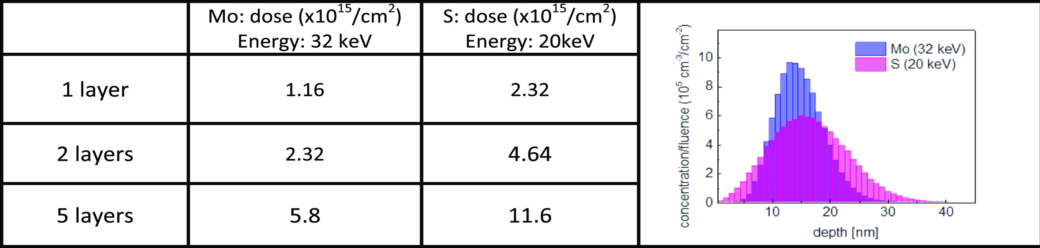
The figure on the right-hand side shows the simulated profiles (using the SRIM software16) of Mo and S inside Al2O3 (amorphous) after implantation at 32 and 20 keV, respectively. For those implantation energies, the common projected range is around 15 nm.
First, we characterized the substrates just after ion implantation. Figure 1 shows a cross section HRTEM observation of the sapphire substrate after the co-implantation of two-layer doses of MoS2 and before any intentional annealing. The cross section (just as all other cross sections in this paper) was prepared by focused ion beam (FIB) machining using an FEI “Scios” dual beam scanning electron microscope/FIB equipment (see the section Methods). The HRTEM image is further analyzed using fast Fourier transforms (FFTs) of chosen regions. First of all, we see that the sapphire substrate has been amorphized by the co-implantation process down to a depth of ∼33 nm, which is about twice the value of the projected ranges shown in Table 1 for S and Mo. Quite interestingly, this depth appears to be constant, defining a remarkably neat, close to flat, and abrupt interface with the still crystalline underlying sapphire. This resembles the situation of Si amorphization, for instance, by As or other heavy dopant implantation, which has been thoroughly studied in the past.14,15
Figure 1.

TEM cross section recorded in the sapphire [1–100] zone axis of an unannealed implanted sample (2-layer doses, S implanted first). (a) HRTEM image. (b) FFTs of the regions squared in (a) (scale bar in 1 is valid for the three FFTs): in FFTs 1 and 2, the diffuse intensity shows that the implanted part of the sapphire substrate is essentially amorphous; in FFT 2, the presence of 0002 reflections at (0.62 nm)−1 (red oval) indicates the early formation of MoS2; in FFT 3, the well-defined zone pattern shows that the substrate just beneath the interface is still single-crystal sapphire.
Another striking feature is that (very) small crystallites of MoS2 can already be observed in the amorphized sapphire even though no intentional annealing was performed at this stage. Those MoS2 crystallites, in the form of few-nanometer, round-shaped precipitates, lie in an ∼10 nm thick region roughly situated in the middle of the amorphized layer, around a depth corresponding to the projected ranges. We note that this is where the concentrations of S and Mo atoms are the highest after implantation and before annealing. This phenomenon is even more pronounced for implantations at higher doses (see Figure S1 of the Supporting Information), where the MoS2 crystallites are much larger and are localized in a 12 nm wide region of the substrate, situated ∼10 nm beneath the surface. Even though the implantation current was kept very low (2.4 × 10¹¹ ions/cm2/s for Mo and 1.7 × 10¹¹ ions/cm2/s for S, see the section Methods), this early MoS2 crystallization is probably due to an ion beam-induced heating phenomenon during ion implantation.17
Figure 2 displays some Raman spectra obtained after various annealing treatments, following the co-implantation of doses corresponding to 5 layers of MoS2 (see Table 1). The E2g1 (around 384 cm–1) and A1g (around 408 cm–1) Raman peaks, which are characteristic of MoS2,18,19 are well resolved. Clearly, the samples annealed at 850 °C for 1 h or at 800 °C for 3 h give the most intense signals, with the smallest full width at half-maximum, which we take as an indication of a better crystallization/larger coverage fraction.20 Note that annealing at 950 °C annihilates the Raman signal of MoS2.
Figure 2.

Raman spectra as a function of annealing temperature for MoS2 samples implanted in sapphire with 5-layer doses. The right-hand side has been separated for the sake of clarity; the color code for the annealing conditions is the same as for the left-hand part of the figure.
Samples co-implanted with 1- and 2-layer doses also exhibit a maximum Raman intensity when the annealing is performed in the 800–850 °C range. However, compared to the 5-layer doses, those Raman intensities are much lower, as shown in Figure S2 of the Supporting Information. Moreover, we have observed that some fractions of the implanted species disappear during annealing, particularly S, probably by out-diffusion. For instance, when one-layer doses are co-implanted, there is no Raman signal appearing at any annealing temperature, unless some sulfur (a few μg) is added inside the ampule before sealing (and before annealing); the S vapor pressure in the ampule (at the annealing temperature) decreases the concentration gradient of the sulfur inside the substrate (an extension of Henry’s law21), thus limiting out-diffusion. The Raman signal shown in the inset of Figure S2 for the 1-layer doses was obtained in those conditions of S addition inside the sealed ampule.
Figure 3 shows a TEM cross section realized after 850 °C annealing (1 h) of a sample co-implanted with 2-layer doses. It came as a surprise to see that, despite the concentration of MoS2 clusters in the central region of the amorphized zone before annealing (Figures 1 and S1), the MoS2 crystallization seems to occur mainly at the interface between the amorphized sapphire and the underlying crystalline part of the substrate.
Figure 3.

TEM cross-sectional view of a sample co-implanted with two-layer MoS2 doses and annealed at 850 °C (1 h) in a sealed quartz ampule. Annealing has been performed with some sulfur (∼10 μg) added in the ampule before sealing it. We note that some MoS2 crystallites, marked by red arrows, are randomly distributed/oriented in the central region of the regrown sapphire.
This means that the crystallites we have observed before annealing were in a metastable state, and most of them have disappeared during annealing. However, we do observe that some MoS2 crystallites, marked by red arrows in Figure 3, are randomly distributed/oriented in the central region of the regrown sapphire. They probably originate from those clusters (observed in Figures 1 and S1) that have managed to reach the critical size necessary for growth. Another observation is that the thickness of the flakes in Figure 3 corresponds to approximately 3 layers of MoS2. However, the MoS2 film is obviously not continuous, covering less than one-half of the interface, which means that some of its constituting elements have either out-diffused or have formed other compounds with Al and/or O. Since, for this particular experiment, we had added some sulfur microparticles inside the ampule before sealing and annealing, we cannot suspect S to have out-diffused from the sapphire during annealing (the equilibrium vapor pressure of S is >1 atm already at 500 °C). We note that Al can react with S, forming, e.g., Al2S3, which can crystallize as a hexagonal allotrope, but we have not detected any Raman signal for this compound in our samples. On the other hand, S can be trapped on defects in the regrown sapphire, forming local Al–S bonds. Also, some of the Mo can be lost to parasitic Mo–O bonds.
Figure 4 shows some TEM cross sectional viewgraphs of a sample co-implanted with 5-layer doses and annealed at 850 °C for 1 h. Again, MoS2 crystallization seems to occur mainly at the interface between the amorphous and crystalline sapphire. It clearly appears that by increasing the implanted doses, we have increased the size of the MoS2 flakes, from ∼15 to 20 nm in Figure 3 to more than 200 nm in Figure 4. As with the situation depicted in Figure 3, in some places, the crystallization did not occur parallel to the interface (see Figure S3, Supporting Information), probably because some of the MoS2 crystallites observed just after implantation (and evidenced in Figure S1) already had a critical size and have managed to grow during the annealing step.
Figure 4.

TEM and STEM cross-sectional viewgraphs of a sample co-implanted with 5-layer doses and annealed at 850 °C (1 h). (a) The lateral extension of a MoS2 flake, here about 220 nm, is much larger than with the two-layer doses (compare with Figure 3, where the extension is at best ∼15–20 nm). (b) HAADF imaging (STEM mode) of a part of the film of (a); the HAADF image is superimposed with EDX images of S, Mo, and Al, clearly showing 5 layers of MoS2. (c) Enlarged view of (b). (d) Layer counting of (b) was performed by contrast analysis.
We note that the MoS2 film seems to develop preferentially parallel to the interface between the amorphous and crystalline sapphire. This point will be further developed in the “Discussion” section.
MoS2 Synthesis When Mo Is Implanted First
For the same implantation energies and doses (Table 1), we observed marked differences in Raman intensity after annealing, depending on whether S was implanted before or after Mo; this is shown in Figure 5. Hence, the implantation order seems to matter.
Figure 5.

Comparison of Raman intensities from five-layer samples where (a) S was implanted first and (b) Mo was implanted first, after the heat treatments indicated in the insets. The ordinate scale is the same for (a,b).
Figure 6 shows a TEM cross section picture of a co-implanted sample (5-layer doses) where Mo was implanted first. Again, we see that the sapphire substrate has been amorphized by the co-implantation process, down to a depth of ∼30 nm, which is very similar to the situation depicted Figure 1, where S was implanted first. Here as well, there is a neat interface with the still crystalline underlying sapphire. However, this interface seems to be more disturbed in places, see the bottom part of Figure 6b where small particles of the starting sapphire protrude from the still crystalline part of the substrate. Also, and as with the situation depicted in Figures 1 and S1, small crystallites of MoS2 can already be observed in the amorphous alumina, even though no intentional annealing was performed at this stage.
Figure 6.

TEM cross section of an unannealed implanted sample (5-layer doses), where Mo is implanted first; sapphire substrate in [11-20] zone axis. (a) General view. (b) Zoom on the amorphized layer. (c) FFTs of the yellow squared areas in (b). Note in the FFT of the amorphous layer, the presence of a ring at 0.61 ± 0.02 nm, characteristic of MoS2 precipitates [red oval in (b)] and the fact that the 2-2010 and 00012 spots have not completely disappeared: they are the remains of a crystalline short-range order in the amorphous layer.
When looking at the Mo-implanted first samples in the TEM, after annealing (850 °C—1 h), see Figure 7, one first observes that the interface with the undamaged sapphire is now rough, in stark contrast with what was observed when S was implanted first (compare Figures 3 and 4 with Figure 7a). Large crystals of MoS2 indeed appear at the interface between damaged and undamaged sapphire; those crystals are relatively thick, and the interface is no longer flat. Thus, implanting Mo first allows one to get larger MoS2 crystals than that obtained by implanting S first (see Raman spectra, Figure 5). In Figure 7, one can also notice that the recrystallized alumina adopted the metastable γ-phase. More details will be given in the Discussion Section.
Figure 7.

TEM cross section of an Mo-implanted-first sample, with five-layer doses, 850 °C, 1 h anneal, oriented in a [1–120] zone axis of sapphire. (a) General view: contrary to the S-implanted-first cases, the interface between the substrate and the recrystallized materials is not flat. (b) HRTEM of a MoS2 crystal at the interface. (c) FFTs of the squared areas in (b), showing the structure of the MoS2 crystal and that of the recrystallized sapphire. The FFT of MoS2 (c-2) exhibits no visible epitaxial relationship; the upper part of MoS2 is superimposed in the beam direction with the recrystallized sapphire.
Discussion
Orientation of the Interfacial MoS2
As the MoS2 orientation has set during nucleation, upon annealing, we start by comparing the distribution of implanted species prior to annealing (Figures 1 and 6) and after annealing (Figures 4 and 7). Obviously, the annealing operation has redistributed matter, allowing it to diffuse to and precipitate at the interface between damaged and undamaged sapphire. The crystallites we have observed before annealing (Figures 1, 6 and S1) have formed at the temperature generated by the ion implantation process, which was probably low; i.e., they have benefited from a large supersaturation (remember that those crystallites appear at a depth corresponding to the projected range, where the concentration of implanted species is the highest), delivering a high density of stable clusters. The lower supersaturation at the higher annealing temperature has the effect of dissolving those clusters, allowing the Mo and S atoms to move to more favorable precipitation places; this low supersaturation has also the effect of limiting the density of nucleation sites, which, in turn, promotes the development of large individual MoS2 crystals. However, we did observe that some MoS2 crystallites, marked by red arrows in Figure 3, were randomly distributed and/or oriented in the central region of the regrown sapphire. As quoted above, they probably originated from those clusters (observed in Figures 1, 6, and S1) that have managed to reach, at the end of the implantation process, a size large enough to avoid dissolution upon temperature increase.
Although several precipitate orientations may be found in the samples we observed, the interfacial MoS2 layers appear to crystallize preferentially with their (0002) planes parallel to the interface between amorphous and crystalline sapphire. Thermodynamically, such an orientation minimizes interfacial energy during nucleation, as the energy of the interface between crystalline and amorphized sapphire is gained in this operation and as the MoS2 (0002) surface, which is maximized, has a low energy (no dangling bonds). Such a scenario assumes that there exists an interface between the damaged and undamaged aluminas; viz., that the damaged alumina has not recrystallized in the continuity of sapphire prior to MoS2 precipitation. Thus, MoS2 precipitation would occur before the amorphized alumina recrystallizes, which is supported by inspection of Figures 1 and 6 where alumina is still amorphous, whereas some small MoS2 crystallites have already appeared, before any intentional annealing. Thus, whatever the implantation conditions, MoS2 appears to precipitate preferentially at the interface between the original sapphire substrate and its part that has been amorphized during implantation. However, there is a marked difference between the situation when S was implanted first, where the interfacial precipitates may extend laterally and remain thin (with a thickness approximately equal to that anticipated by the choice of implantation doses, Figures 3 and 4) and the case of Mo implanted first, where those precipitates are shorter and thicker (Figure 7). Quite remarkably, the interface between the two aluminas after annealing is correlatively flat in the first case and rough in the second one.
To understand this difference, let us briefly discuss the phase of MoS2 and the orientation of the layers in their plane. First of all, we emphasize that considering the structure of the edges of TMDCs (e.g., zigzag or armchair for faceted crystals), epitaxy can only happen through lateral bonding with atoms of the substrate, thus eliminating dangling bonds. Indeed, we note that, when the sapphire is in a zone axis in the TEM, MoS2 rarely is; the (0002) planes are visible almost all the time, but the atomic order in the planes is generally not. The periodic contrasts that sometimes appear are most often associated with superimposed sapphire in the beam direction. Thus, the MoS2 layers are generally not aligned with their substrate in the plane. We found a precipitate in the zone axis in only one case where the substrate was not in the zone axis (see Supporting Information, Figure S4). The particular precipitate orientation in that case allowed us to characterize the phase of the MoS2, which was the equilibrium hexagonal 2H phase (Figure S4).
Although we found only a few visible vertical planes of the MoS2 2H structure, we could measure the (0002) interplanar distance in many occurrences. We found it to be systematically larger than the theoretical 2H interplanar distance, by as much as 10%. By analyzing the precipitate lateral walls in the Mo-implanted-first samples, we found them to be epitaxially related to the nearby sapphire substrate with one (0002) plane corresponding to three (0006) planes in sapphire. Three times the (0006) interplanar distance in sapphire is indeed 0.65 nm, which represents a 6% dilatation for MoS2. Let us mention here that an equivalent geometry with the regrown γ-phase of alumina was rarely observed (see discussion on the γ-phase below). Indeed, in this case, the (222) (0.228 nm) and (111) (0.456 nm) planes replace the (0006) of sapphire; they are less favorable for this type of fit, as three times the (222) distance does not represent a crystalline period and as that hypothetical period would correspond to a 11.2% dilatation.
Anyway, one can keep in mind that large variations occur in the interplanar MoS2 (0002) distance, most likely thanks to the weak van der Waals binding between the MoS2 layers. One could think of intercalation of foreign atoms between the MoS2 planes, allowing the system to adjust the interplanar distance to the local tilt conditions between the precipitates and alumina.
To summarize, the interaction of the MoS2 layers with the alumina host appears to be weak in the plane, in accordance with the absence of dangling bonds on the MoS2 (0002) surfaces. In contrast, it is stronger on the sides of those layers, especially with the α-alumina substrate, generating a vertical periodic connection to the basal alumina planes. One may note that this is particularly the case in the Mo-implanted-first samples, where the interface provides lateral sapphire walls. In the S-implanted-first samples, the flatter interface provides less such nucleation places. Interestingly, although this absence decreases the amount of crystalline MoS2, it opens the way to lateral growth of this material in the form of large 2D layers.
Structure of the Recrystallized Sapphire
Let us now analyze the way alumina recrystallizes. To summarize, even if the recrystallized alumina sometimes recovers the α-phase of the substrate, often with a twin relationship with the latter, most of the time, it chooses the metastable γ-phase. It does so with a natural epitaxial relationship: <111>, <110> and <211> cubic axes, respectively, parallel to the <0001>, <1–100> and <11–20> hexagonal axes of the rhombohedral α-Al2O3 substrate (Figure 8). These specific phase and orientation occur on top of MoS2 layers (Figure 7) as well as directly on the (0006) surface of undamaged sapphire (Figure 8). We note that this configuration preserves the continuity of the compact stacking of oxygen ions.
Figure 8.

HRTEM cross section of the interface between the original and recrystallized sapphire. (a) HRTEM image. (b,c) FFTs of, respectively, the recrystallized film and the original sapphire. Same sample as in Figure 7. Note the coincidence between the −3300 and 4–40 spots in the Fourier spectra, corresponding to the planes underlined in yellow in (a).
Let us mention that this type of interface, although illustrated in Figure 8 by an example in the Mo-implanted-first sample, is more common in the S-implanted-first samples. The occurrence of γ-alumina upon recrystallization is a well-known phenomenon22 occurring as kinetically favored compared to α-alumina. Thanks to this preference, an interface remains after annealing between the recrystallized and undamaged sapphire, which could, perhaps, be used for further redistribution of the implanted species.
Finally, we note that the 850 °C annealing operation does not always recrystallize the amorphized sapphire, especially in the case of the Mo-implanted-first samples. The pictures of Figure 9, taken with the same sample as in Figures 7 and 8, show how variable the structure of amorphized alumina can be after annealing, in the configuration where the interface is very rough. In this image, that structure appears to remain amorphous-like in different places, including places in contact with MoS2 and places in contact with the sapphire substrate.
Figure 9.

HRTEM cross section showing that the amorphized sapphire has stayed amorphous upon annealing, on top of MoS2 layers, as well as on top of sapphire. Same sample as that in Figures 7 and 8.
Roughness of the Amorphous–Crystal Interface after Annealing When Mo Is Implanted First
As quoted above, there is a striking difference in the structure of the interface between amorphous and crystalline sapphire after annealing, depending on whether S or Mo is implanted first. When S is implanted first, the interface is flat and the MoS2 crystallites tend to be thin, with a thickness roughly corresponding to the chosen doses (Figures 3 and 4); when Mo is implanted first, the MoS2 crystals are much thicker; they do not preferentially develop at the interface between amorphous and crystalline sapphire, and the latter appears extremely rough after annealing.
First, we note that Mo atoms are 3 times heavier than S atoms. Hence, Mo atoms will be much more efficient at displacing target atoms than S atoms. When S is implanted first, the sapphire matrix is already highly damaged at the time Mo implantation is performed. Hence, Mo atoms impinging on atoms of the target cannot propel those atoms (recoil atoms) deep inside the substrate by channeling. The situation is different when Mo is implanted first, since the sapphire matrix is originally devoid of implantation-induced defects, so that recoil atoms can be channeled and may induce defects deeper in the substrate, leading to a more perturbed, broader, and less flat interface (see Figure 6b). Such a perturbed interface would provide more nucleation sites for MoS2, thus leading to thicker layers.
An alternative or additional phenomenon that may also be responsible for the differences observed when Mo or S is implanted first is the heating induced by the ion beam, which we have also argued above to be responsible for some MoS2 early crystallization observed in the as-implanted state. Although the fluence rates were low (see Methods), considering the higher energy and fluence rate of the Mo implants, the deposited power density (power per unit area) is more than twice as large for the Mo implants compared to S. This significant difference in deposited power density can be expected to result in a higher local temperature during the Mo implantation, which, in turn, may induce some enhanced diffusion of the Mo atoms, leading to local accumulation and to a different crystallization behavior for MoS2.
Conclusions
We studied the synthesis of MoS2 layers by ion implantation of the parent atoms (Mo and S) into chemically neutral sapphire. Various doses have been tested, corresponding to atom counts of 1 to 5 layers of MoS2. The sapphire was (0001)-oriented. We have first observed that the subsurface region of the sapphire substrates is amorphized by the ion implantation process, even for low doses corresponding to two-layer counts of MoS2. An annealing step in the 800–850 °C temperature range results in the precipitation of MoS2 crystals inside the sapphire. Those crystals are preferably aligned at the interface between the amorphous sapphire and the remaining substrate. When S is implanted first, large and thin MoS2 flakes (larger than 200 nm for implantation doses corresponding to 5 MoS2 layers) can be obtained after annealing. When Mo is implanted first, the MoS2 flakes are (much) thicker, and the interface with the underlying sapphire is rough. Hence, the order of implantation is an important parameter for the synthesis of MoS2 under the conditions used in this work. Finally, Figure S5 of the Supporting Information shows a possible fabrication sequence for a field effect transistor using recrystallized sapphire as a gate dielectric material.
Methods
Ion Implantation
Ion implantation was performed using a Danfysik 1090 implanter (mass resolving power M/ΔM ∼150–250), at the Ion and Molecular Beam Laboratory, KU Leuven. Mo+ ions were implanted at 32 keV with a fluence rate of 2.4 × 10¹¹ ions/cm2/s, whereas S+ ions were implanted at 20 keV with a fluence rate of 1.7 × 10¹¹ ions/cm2/s. The implantation was performed at room temperature (without active heating nor cooling) in a vacuum chamber with a pressure of approximately 1 × 10⁻⁵ mbar.
FIB Preparation of TEM Lamellas
The cross section lamella preparation for all the considered samples was performed using Thermo Fisher Scios dual beam equipment. Since all the samples were synthesized using sapphire substrates, we used a high current of the Ga ion source during the sample preparation.
TEM Analyses
TEM was performed with four pieces of equipment: (i) a Thermo Fisher Themis working at 200 kV, equipped with a Cs-corrector of the condenser system and a ChemiSTEM Super-X four-quadrant energy-dispersive X-ray (EDX) detector, for high-resolution HAADF and chemical images, (ii) a Thermo Fisher Titan working at 300 kV, with a Cs-corrector of the objective lens, for high-resolution images, (iii) a Thermo Fisher Themis working at 300 kV, for standard high-resolution images, and (iv) a Jeol 2010F for standard TEM.
Acknowledgments
This work was performed under the SIMPLANT (FLAG-ERA 2017 program) and 2D-on-Demand projects, overseen by the French National Research Agency (ANR). R.B., I.V., I.F., J.L.M., P.L., and D.P. would also like to acknowledge financial support from the French state managed by the National Research Agency under the Investments for the Future program under the references ANR-10-EQPX-50 pole NanoTEM and Pole NanoMAX. Part of TEM analyses were performed at the Centre Interdisciplinaire de Microscopie Electronique de l’X (CIMEX), which is gratefully acknowledged. L.M.C.P., H.B., and R.V. also acknowledge financial support from the KU Leuven and the Research Foundation Flanders (FWO, Belgium).
Supporting Information Available
The Supporting Information is available free of charge at https://pubs.acs.org/doi/10.1021/acsomega.3c03179.
Additional TEM characterization after 5-layer dose implantations and before annealing; comparison of Raman signals from MoS2 synthesized with 1-, 2-, and 5-layer doses; additional TEM observation of “parasitic” MoS2 growth away from the interface; structure of the MoS2 determined by HRTEM; and possible transistor configuration using the recrystallized sapphire as the dielectric gate (PDF)
Author Present Address
# TE-OX, 21 Rue Jean Rostand, 91400 Orsay, France
Author Present Address
¶ Safran Electronics & Defense, 100 Av de Paris, 91344 Massy, France.
Author Present Address
∇ CRHEA, CNRS, UMR7073, Rue Bernard Grégory, 06905 Sophia-Antipolis Cedex, France.
The authors declare no competing financial interest.
Supplementary Material
References
- Zhu K.; Wen C.; Aljarb A. A.; Xue F.; Xu X.; Tung V.; Zhang X.; Alshareef H. N.; Lanza M. The Development of Integrated Circuits Based on Two-Dimensional Materials. Nat. Electron. 2021, 4, 775–785. 10.1038/s41928-021-00672-z. [DOI] [Google Scholar]
- Xia F.; Wang H.; Xiao D.; Dubey M.; Ramasubramaniam A. Two-Dimensional Material Nanophotonics. Nat. Photonics 2014, 8, 899–907. 10.1038/nphoton.2014.271. [DOI] [Google Scholar]
- Schaibley J. R.; Yu H.; Clark G.; Rivera P.; Ross J. S.; Seyler K. L.; Yao W.; Xu X. Valleytronics in 2D Materials. Nat. Rev. Mater. 2016, 1, 16055. 10.1038/natrevmats.2016.55. [DOI] [Google Scholar]
- Geim A. K.; Grigorieva I. V. Van Der Waals Heterostructures. Nature 2013, 499, 419–425. 10.1038/nature12385. [DOI] [PubMed] [Google Scholar]
- Choukroun J.; Pala M.; Fang S.; Kaxiras E.; Dollfus P. High Performance Tunnel Field Effect Transistors Based on In-Plane Transition Metal Dichalcogenide Heterojunctions. Nanotechnology 2019, 30, 025201. 10.1088/1361-6528/aae7df. [DOI] [PubMed] [Google Scholar]
- Li H.; Li Y.; Aljarb A.; Shi Y.; Li L.-J. Epitaxial Growth of Two-Dimensional Layered Transition-Metal Dichalcogenides: Growth Mechanism, Controllability, and Scalability. Chem. Rev. 2018, 118, 6134–6150. 10.1021/acs.chemrev.7b00212. [DOI] [PubMed] [Google Scholar]
- Choudhury T. H.; Zhang X.; Al Balushi Z. Y.; Chubarov M.; Redwing J. M. Epitaxial Growth of Two-Dimensional Layered Transition Metal Dichalcogenides. Annu. Rev. Mater. Res. 2020, 50, 155–177. 10.1146/annurev-matsci-090519-113456. [DOI] [Google Scholar]
- Li X.; Cai W.; An J.; Kim S.; Nah J.; Yang D.; Piner R.; Velamakanni A.; Jung I.; Tutuc E.; et al. Large-Area Synthesis of High-Quality and Uniform Graphene Films on Copper Foils. Science 2009, 324, 1312–1314. 10.1126/science.1171245. [DOI] [PubMed] [Google Scholar]
- Tsai H.-S.; Liou J.-W.; Wang Y.-C.; Chen C.-W.; Chueh Y.-L.; Hsiao C.-H.; Ouyang H.; Woon W.-Y.; Liang J.-H. Vertical Al2Se3/MoSe2 Heterojunction on Sapphire Synthesized Using Ion beam. RSC Adv. 2017, 7, 10154–10157. 10.1039/C6RA28273C. [DOI] [Google Scholar]
- Tsai H.-S.; Liou J.-W.; Setiyawati I.; Chiang K.-R.; Chen C.-W.; Chi C.-C.; Chueh Y.-L.; Ouyang H.; Tang Y.-H.; Woon W.-Y.; et al. Photoluminescence Characteristics of Multilayer HfSe2 Synthesized on Sapphire Using Ion Implantation. Adv. Mater. Interfaces 2018, 5, 1701619. 10.1002/admi.201701619. [DOI] [Google Scholar]
- Rubin L.; Poate J.. Ion Implantation in Silicon Technology. 2003, https://www.axcelis.com/wp-content/uploads/2019/02/Ion_Implantation_in_Silicon_Technology.pdf (accessed Apr 21, 2023).
- Baraton L.; He Z.; Lee C. S.; Maurice J.-L.; Cojocaru C. S.; Gourgues-Lorenzon A.-F.; Lee Y. H.; Pribat D. Synthesis of Few-Layered Graphene by Ion Implantation of Carbon in Nickel Thin Films. Nanotechnology 2011, 22 (8), 085601. 10.1088/0957-4484/22/8/085601. [DOI] [PubMed] [Google Scholar]
- Baraton L.; He Z. B.; Lee C. S.; Cojocaru C. S.; Châtelet M.; Maurice J.-L.; Lee Y. H.; Pribat D. On the Mechanisms of Precipitation of Graphene on Nickel Thin Films. Europhys. Lett. 2011, 96 (4), 46003. 10.1209/0295-5075/96/46003. [DOI] [Google Scholar]
- Williams J. S. Ion implantation of semiconductors. Mater. Sci. Eng., A 1998, 253, 8–15. 10.1016/S0921-5093(98)00705-9. [DOI] [Google Scholar]
- Christel L. A.; Gibbons J. F.; Sigmon T. W. Displacement Criterion for Amorphization of Silicon During Ion Implantation. J. Appl. Phys. 1981, 52, 7143–7146. 10.1063/1.328688. [DOI] [Google Scholar]
- Ziegler J. M.Stopping and Range of Ions in Matter. 2023, http://www.srim.org/ (accessed Apr 21, 2023).
- Parry P. D. Target Heating During Ion Implantation. J. Vac. Sci. Technol. 1976, 13, 622–629. 10.1116/1.569046. [DOI] [Google Scholar]
- Lee C.; Yan H.; Brus L.; Heinz T. F.; Hone J.; Ryu S. Anomalous Lattice Vibrations of Single-and Few-Layer MoS2. ACS Nano 2010, 4 (5), 2695–2700. 10.1021/nn1003937. [DOI] [PubMed] [Google Scholar]
- Molina-Sanchez A.; Wirtz L. Phonons in Single-Layer and Few-Layers MoS2 and WS2. Phys. Rev. B: Condens. Matter Mater. Phys. 2011, 84, 155413. 10.1103/PhysRevB.84.155413. [DOI] [Google Scholar]
- Lukas S.; Hartwig O.; Prechtl M.; Capraro G.; Bolten J.; Meledin A.; Mayer J.; Neumaier D.; Kataria S.; Duesberg G. S.; Lemme M. C. Correlating Nanocrystalline Structure with Electronic Properties in 2D Platinum Diselenide. Adv. Funct. Mater. 2021, 31 (35), 2102929. 10.1002/adfm.202102929. [DOI] [Google Scholar]
- Deal B. E.; Grove A. S. General Relationship for the Thermal Oxidation of Silicon. J. Appl. Phys. 1965, 36, 3770–3778. 10.1063/1.1713945. [DOI] [Google Scholar]
- Levin I.; Brandon D. Metastable Alumina Polymorphs: Crystal Structures and Transition Sequences. J. Am. Ceram. Soc. 1998, 81, 1995–2012. 10.1111/j.1151-2916.1998.tb02581.x. [DOI] [Google Scholar]
Associated Data
This section collects any data citations, data availability statements, or supplementary materials included in this article.