Abstract
We introduce an optical microscopy technique, circularly polarized microscopy or CPM, able to afford spatially resolved electronic circular dichroism (ECD) of thin films of chiral organic semiconductors through a commercial microscope equipped with a camera and inexpensive optics. Provided the dichroic ratio is sufficiently large, the spatial resolution is on the order of the μm and is only limited by the magnification optics integrated in the microscope. We apply CPM to thin films of small chiral π-conjugated molecules, which gave rise to ordered aggregates in the thin layer. Primarily, conventional ECD can reveal and characterize chiral supramolecular structures and possible interferences between anisotropic properties of solid samples; however, it cannot generally account for the spatial distribution of such properties. CPM offers a characterization of supramolecular chirality and of commingling polarization anisotropies of the material, describing their local distribution. To validate CPM, we demonstrated that it can be adopted to quantify the local ECD of samples characterized by intense signals, virtually on any standard optical microscope.
Keywords: optical microscopy, chirality, ECD, thin films, π-conjugated materials
1. Introduction
There is tremendous interest in the development of organic materials for applications in optical and electronic (optoelectronic) devices.1,2 Both low molecular weight and macromolecular organic semiconductors are one key point of the materials,3,4 aiming at replacing inorganic systems based on silicon. This responds to several needs: foldable devices; avoiding the use of rare elements; ease of fabrication; reduced impact at the end of life.1 Furthermore, crucial features, such as band gap, optical properties or charge mobility, can be modulated by chemical modifications with standard organic chemistry reactions. One aspect that needs to be carefully kept under control is the structural homogeneity of thin films, because this can affect their performances,5 sometimes with the appearance of new features.6,7 The first tool to check this aspect is optical microscopy. Primarily, it reveals thickness differences and, in the case of blends, phase segregations.8 In the following, we shall deal with thin layers made by spin coating glass substrates with solutions of small organic chromophoric molecules. Under these conditions, compositional and thickness homogeneities are ensured. However, one aspect that remains open is the supramolecular organization. One may expect that, during solvent evaporation and during post-deposition annealing, molecules order themselves, at least to some extent. If multiple aggregation modes coexist, polymorphs can give rise to phase boundaries, which one would like to visualize.9 Unfortunately, standard microscopy, even taking advantage of phase contrast techniques, does not meet this need, because the variation of refractive index in response to different local order is not sufficiently pronounced. On the contrary, thanks to supramolecular chirality, ordered structures can lead to strong discrimination of light circular polarization, both in absorption and in emission.6 At least in absorption, in the following, we shall demonstrate how this can be revealed on microscopic scale by simple modifications of a standard optical microscope, providing useful information, which would not be accessible otherwise.
The differential absorption of left and right circularly polarized (CP) light in the UV–vis spectral range gives rise to electronic circular dichroism (ECD), which is one of the most significant manifestations of chirality in light–matter interactions.10 It provides important information regarding the absolute configuration of chiral molecules bearing chromophores.11−13 Conformational aspects can also be rationalized by ECD characterization.14 Besides molecular insights, ECD is even a fundamental tool to investigate noncovalent chiral assemblies or aggregates.15
ECD finds application in the study of small biomolecules13,16 and biomacromolecules17 and in the investigation of their interactions.18 ECD is also widely adopted in the investigation of chiral inorganic metal complexes.19 More recently, it found a role in the characterization of synthetic organic chiral π-conjugated systems designed for optoelectronic applications.20,21 Within this field, CD is fundamental to understand the chiral aggregation modes at various hierarchical levels of these materials in thin film, which represents the most common form in which they are employed in optoelectronic devices.3,22
Getting information on the spatial distribution of ECD on materials of various natures sheds light on samples presenting chirality at a particular scale but characterized by its absence on a different hierarchical level.23 ECD can be extremely sensitive to supramolecular chiral arrangements, and for this reason, it is ideal to investigate a difficult dimensional range, going from the subnm to the μm scale throughout several orders of magnitude. Unfortunately, commercial benchtop ECD spectropolarimeters are not conceived for performing localized analysis and they are unable to detect submm spatial distributions of chiral aggregates, as the typical observation area is about 3 × 3 mm. Selecting a restricted area by covering the surrounding while using a conventional light source would not solve the issue, since not enough photons will reach the photomultiplier tube to be detected, so a collimation of the light beam and a powerful source are required.
An idea of ECD microscopy was first developed several years ago to allow measurements on single eukaryotic cells.24 More recently, the unique highly collimated synchrotron radiation circular dichroism (SRCD) of Diamond Light Source B23 beamline allowed us to scan the surface of materials and to produce spatially resolved ECD maps. This takes advantage of a high density photon flux joint with the optical elements and the electronics typical of conventional spectropolarimeters, such as photoelastic modulator (PEM) and lock-in detection. This concept found application in the spatially resolved ECD characterization of chiral π-conjugated materials in thin film25−27 with a maximum spatial resolution of about 50 μm, the so-called ECD imaging or ECDi.28 In these conditions, one can very accurately record localized ECD spectra over the whole UV–vis spectral range and with full sensitivity, allowing the accurate detection and quantification of even small signals. The current limitation of SRCD using B23 is not capturing features smaller than 50 μm.
Okamoto and co-workers designed a near-field ECD microscope keeping all the optical components of commercial instruments, which overcame this limitation, reaching a spatial resolution on the nanoscale. These authors integrated this instrumentation with a XY-stage to be able to scan the spatial distribution of CD signals of chiral metal 2D nanostructures29,30 as well as to show the local ECD distribution of globally ECD-inactive gold 2D nanostructures.31 Although powerful, this technique suffers from the limitation of requiring specialized equipment not readily available in every laboratory.
All the mentioned setups capable of measuring spatially resolved ECD adopt a linear polarizer followed by a photoelastic modulator (PEM) to generate circularly polarized light, as commercial spectropolarimeters.32 In this manner, the light is continuously modulated between left and right handedness, passing through linear polarization (LPn). If part of the LPn is retained because of possible imperfections in the optics and the electronics, the outcoming beam will be elliptically polarized and the resulting ECD measurements in transmission may be affected by instrumental artifacts because of the interaction with possible linear anisotropies present in the sample and in the detection optics.33,34 A practical solution is isolating in time left CP (LCP) and right CP (RCP) light (the so-called discrete approach). It was successfully applied to a map at a sub-μm scale chiral chromium complex layer,35 thin films of plasmonic nanocomposites,36 and organic materials showing strong chiral induced spin selectivity.37 The final solution to the problem of spurious contributions to ECD requires the determination of the full Mueller matrix, which is by far a nonstandard technique.38−40
Despite the progress of spatially resolved ECD, all the setups cited above require the utilization of a XY-stage to move the sample so that the signal may be recorded point by point, requiring long acquisition times. A discrete ECD microscopy technique adopting a CMOS camera as the detector and, thus, simultaneously acquiring the signal over all the pixels of the area studied was reported by Kahr et al. to elucidate the enantiomorphous twinning of crystals of 1,8-dihydroxyanthraquinone.41 Besides ECD, microscopies based on the differential emission of left and right CP light (circularly polarized luminescence) from emitting chiral compounds were reported.42−45
Among various forefronts of current research in the field of chiral organic materials for optoelectronic applications, there is the quest for systems affording conspicuous discrimination of light circular polarization. These materials will find application for fabricating devices responding to or producing CP light, such CP-sensitive organic transistors21 or circularly polarized OLEDs (CP-OLEDs).46 In these conditions, giant ECD signals arise and the use of sophisticated polarization elements for ECD detection and quantification may be circumvented, at least within well-defined limits of accuracy and of wavelength selection.
In the following, we show that a regular microscope equipped with a commercial camera and inexpensive optics can be successfully employed to obtain ECD mapping with a μm scale resolution of materials characterized by intense ECD signals. In this way, circularly polarized microscopy (CPM) images of chiral materials may be easily obtained.
Herein, we have applied a discrete ECD microscopy method to simultaneously reveal the local signals at a μm spatial resolution on thin films made of compounds 1 and 2. Compound 1, based on carbazole, provides a very homogeneous film and will be used to demonstrate the principle. On the contrary, compound 2, (S,S)-PTPO (phenylene bis-thiophenyl propynone), is an organic chiral π-conjugated molecule previously reported by us and fully characterized with standard chiroptical techniques as well as by scanning electron microscopy.47 Thin films of 2 are characterized by a very uncommon feature of the apparent ECD spectrum. In fact, the ECD signals instead of being independent of sample orientation, as one would expect, invert upon sample flipping. On similar compounds, we had put forward that this peculiarity arises from a self-organization into ordered domains.20,48 This apparent, nonreciprocal, ECD spectrum, which has also been referred to as LDLB coupling, can have paramount consequences in devices, such as CP-OLEDs47,49 or resonating cavities.50 Its foundations are rooted in classical literature,33,51,52 but they have been the object of recent theoretical investigation by Tempelaar and co-workers, who determined minimal conditions for the appearance of this effect.53
Here, we found that, despite appearing homogeneous when retro-illuminated with unpolarized light, 2 has a complex CP light-sensitive texture deeply affecting the resulting properties. Moreover, it presents the advantage of a sizable chiroptical activity.
2. Results and Discussion
Before undertaking any more significant and quantitative analysis, we must demonstrate and validate the setup and the subsequent data elaboration to extract ECD information by means of CPM. Compound 1, shown in Scheme 1, is known to produce homogeneous films3 and can be used as reference.
Scheme 1. Carbazole-Based Material 1 and (S,S)-PTPO 2 Chemical Structures.
Interestingly, thin films of compound 1 are photo- and electroluminescent and they display circularly polarized (CP) luminescence, which allowed us to produce the first CP-OLED where the emitting layer is made of a single small organic molecule, rather than one of the usual blends of different components.3
We prepared the film samples by spin coating a dichloromethane solution of the material to be analyzed on a glass substrate.
With reference to Figure 1, our CPM setup enables the detection of the differential transmission of CP light as described in the following.
Figure 1.
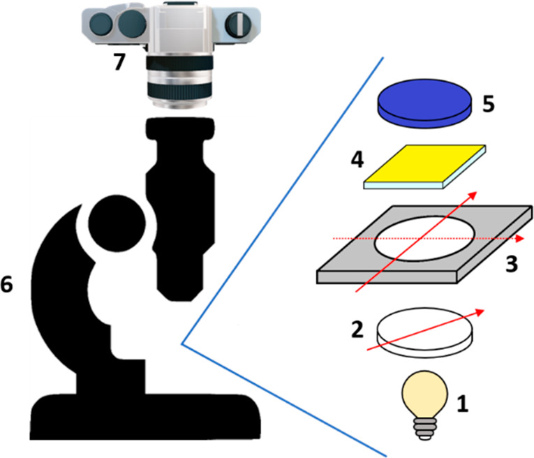
Schematic representation of the optical setup adopted. (1) White light source, (2) linear polarizer, (3) QWP rotated at 90° steps, (4) thin film sample, (5) 450 nm blue bandpass filter, (6) Zeiss Discovery V8 microscope, (7) digital camera.
A Zeiss Discovery V8 microscope has a housing to host a linear polarizer (LP) above the lamp, which can be used to obtain linearly polarized light along a known direction. To achieve CP-sensitive images, we placed the LP in its housing and above this we placed a birefringent quarter-wave plate (QWP). By positioning the QWP fast axis at +45° or −45° with respect to the LP axis, RCP and LCP back-illumination was generated (Figure 1). It is important to highlight that the transmission/DIC imaging de Sénarmont compensator of the microscope was not in use. The absence of this component allowed a reliable chiroptical selection. The analysis of a pair of pictures taken with RCP and LCP illumination provides quantitative data of the CP-selective transmittance of the thin film analyzed.
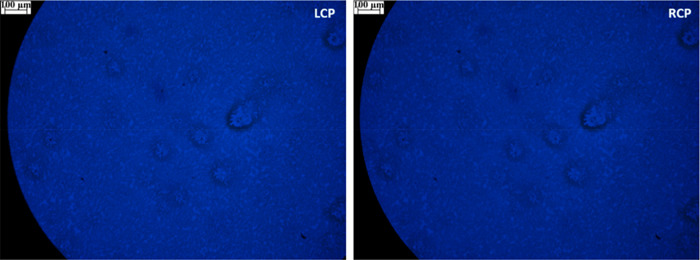
The two pictures shown in Figure 2 are taken under LCP and RCP light illumination of 1 thin film, respectively. Overall, one may appreciate that the film is indeed homogeneously dispersed, apart from a few spots. By comparing these two pictures, we may observe the presence of a slightly different hue, which can be related to the differential transmission of the two CP light beams, due to the sample ECD. This quantity is the dimensionless differential absorbance between LCP (AbsL) and RCP (AbsR) light:54
| 1 |
The differential transmittance of LCP and RCP of a homogeneous sample can be extrapolated from the ECD spectrum measured with a standard benchtop spectropolarimeter, which is reported for compound 1 in Figure S1b and displays a negative signal around 450 nm. Above this wavelength, both absorbance and ECD rapidly decay (Figure S1). To match the same wavelength with our microscope, we placed an Edmund Optics bandpass filter centered at 450 nm (fwhm = 80 nm) above the film (Figure 1) and we obtained the set of images in Figure 2. By comparing the LCP and RCP retro-illuminated images in Figure 2, we notice that they show a small but clear difference in hue, which is related with the sample ECD. In particular, the LCP backlit picture appears brighter than the RCP backlit one, meaning that AbsR > AbsL, so that the ECD is negative, in agreement with the ECD spectrum recorded with a standard instrument.
Figure 2.
Microscopy images of compound 1 thin film acquired backlighting with LCP and RCP light in the blue region (450 nm, fwhm = 80 nm).
The spectrum in Figure S1b shows a ΔAbs of about −0.013 at 450 nm. With I0L and I0R defined as the intensities of incident LCP and RCP light and IL and IR defined as the intensities exiting the film, we have
| 2 |
Temporarily assuming that I0L = I0R, it follows:
| 3 |
With ΔAbs = −0.013, we derive
| 4 |
That is, we predict that at 450 nm the intensity of LCP light must be about 3% stronger than that of RCP light, which can indeed be appreciated in the LCP labeled picture of Figure 2, appearing with a slightly lighter hue than the RCP one. Given the small difference, any quantitative analysis is precluded.
After this preliminary investigation on a homogeneous sample, we faced the more complex case of a thin film of product 2, which we define also as (S,S)-PTPO. The compound 2 thin film was thermally treated at 80 °C for 1 h, as reported in our previous work.47
In standard bright-field microscopy with unpolarized light (Figure 3), apart from some visible and clearly discernible scratches and imperfections on the surface, the film appears homogeneous.
Figure 3.
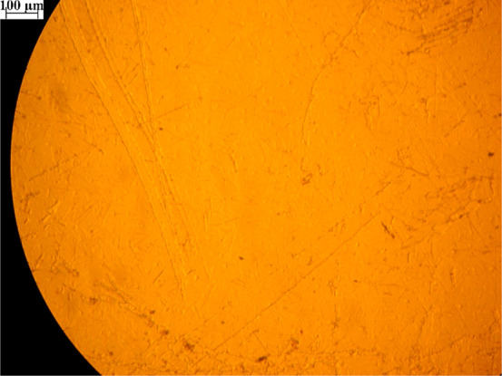
Bright-field microscopy image of (S,S)-PTPO thin film (sample backlit with unpolarized light).
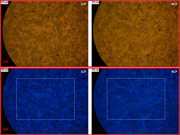
Oppositely, when the film is retro-illuminated with CP light, its partition into grains becomes evident. We can appreciate a remarkable contrast with sharp polygonal boundaries among regions which appear more transparent to LCP light and other ones to RCP light. Such grain-like structures of approximately 100 μm in size are comparable with the domains previously observed in HR-TEM microscopy.47 This is best observed by taking into account pictures of the same film area which are retro-illuminated with opposite handedness of CP light (Figure 4a). In fact, an inspection of the two pictures reveals domains that are bright yellow when the sample is backlit with LCP light but become darker when the sample is backlit with RCP light and vice versa. To summarize the concept and relate it to ECD, grains that appear darker when retro-illuminating with LCP light preferentially absorb this circular polarization, so that AbsL > AbsR and ECD > 0. Vice versa, grains that appear darker when retro-illuminating with RCP light are characterized by AbsR > AbsL and ECD < 0.
Figure 4.
Microscopy images of (S,S)-PTPO thin film (a) acquired backlighting with LCP and RCP white light; (b) acquired backlighting with LCP and RCP light in the blue region (450 nm, fwhm = 80 nm). The white dashed rectangles in the blue region images indicate the clippings considered for the calculation of ECD.
We can appreciate that the heterogeneity characterizing (S,S)-PTPO 2 is absent in the pictures discussed for compound 1.
For 1, we had a homogeneous sample with an identical ECD spectrum for every point of the film. On the contrary, for (S,S)-PTPO, the ECD measured on a large surface (i.e., with a standard spectropolarimeter, Figure S2b) is the result of an average of very different values, not only in magnitude but even in sign.
After this qualitative observation, we managed to quantify the ECD of (S,S)-PTPO at the same spatial resolution of the pictures acquired.
Nonetheless, we observe that above 450 nm the total absorbance of this film quickly decays to zero (Figure S2a) and, for this reason, we chose again to adopt a 450 nm bandpass filter.
Essentially, we repeated the same experiments as described above, taking pictures of the sample and of the blank, upon illumination with LCP and RCP light, as shown in Figure 4b.
The domains are evident also in the blue spectral region (Figure 4b). We then isolated two superimposable rectangular selections on both pictures of Figure 4b to quantify the ECD exclusively on the chosen area (Figure S3a). The clippings were converted in matrices of total intensities, corresponding to black and white (BW) images (Figure S3b).
The spatially resolved ECD matrix (ECD) has been calculated following its definition in eq 1, in which the absorbances relative to the two circular polarizations are obtained through the incoming and outcoming light intensity matrices with respect to the sample. IL and IR are, respectively, the LCP and RCP outcoming light intensity matrices, while I0L and I0R are the respective incoming light intensity matrices. Each element ecdi,j of ECD has been obtained from the corresponding elements in the light intensity matrices by the following equation:
| 5 |
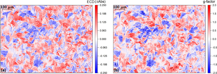
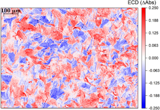
We obtained the incoming light intensities (I0L/R) through the acquisition of images of blank glasses illuminated with LCP or RCP light, while keeping the 450 nm bandpass filter. The same rectangular selections as in Figure 4b were converted into BW total light intensity matrices. After the calculation of ECD from eq 5, the matrix was converted back to a spatially resolved map at the same resolution of the original images adopted for the light intensity estimation (Figure 5a). As hypothesized earlier through the observation of images reported in Figure 4, the ECD map clearly shows the presence of an actual separation of the material among domains with positive ECD and domains with negative ECD. The domains depicted in red in Figure 5a are characterized by positive ECD, therefore by AbsL > AbsR. Vice versa, for the blue domains in the same figure (negative ECD), AbsR > AbsL. The intensity in ΔAbs within each domain is reaching absolute values of ∼0.2, considerably high if compared with what is commonly found for organic chiral π-conjugated molecules with similar structural design in thin film.6
Figure 5.
(a) ECD image of the area of interest of (S,S)-PTPO 2 thin film. Domains with AbsL > AbsR (red) can be clearly distinguished from domains with AbsR > AbsL (blue). (b) g-factor image of the same area. The g-factor, in the case of some of the distinguishable domains, is reaching values close to theoretical maximum absolute value of 2.
At this point, we must give an estimation of the sensitivity and limit of detection of the procedure we adopted to quantify the spatially resolved ECD using the setup proposed. In 32-bit gray scale representation, each value has 3 significant divisions per unit; therefore, the intensity of each pixel is mapped onto 768 overall divisions. This scale of gray sets a theoretical limit to the smallest detectable ECD. In optimal absorbance conditions (i.e., Abs ∼ 0.7–0.8), such resolution corresponds to a minimum detectable ECD of 2.7–3.5 × 10⁻³ (corresponding to 90–110 mdeg of ellipticity) and to a dissymmetry factor (see below) of approximately 5 × 10⁻³. Although this minimum value is relatively large compared to most dedicated ECD instruments, it is completely suitable for the task at hand. Moreover, the use of static optics (QWP), as opposed to a photoelastic modulator, poses more stringent limitations on the smallest reliably measurable dissymmetry factor, which we can estimate in the order of 10–2.
A convenient and alternative metric to quantify the ECD is the absorption dissymmetry factor (gabs). This parameter is defined as the ECD signal (reported in ΔAbs) normalized on the overall absorbance, so it is in principle independent of sample thickness (eq 6).
| 6 |
The g-factor can assume values comprised between −2 and +2, with −2 meaning the material is exclusively absorbing RCP light and +2 meaning the material is exclusively absorbing LCP light. We calculated the g-factor matrix G, to be then converted into the relative map, by taking into account IL, IR, I0L, and I0R elements already adopted for the calculation of ECD elements in eq 5. The overall absorbance matrix (relative map reported in Figure S4) has been calculated as the average between LCP and RCP light absorbances, as reported in eq 6. From the combination of eqs 5 and 6, we obtained the G element gi,j as follows:
 |
7 |
The matrix G obtained from eq 7 was consequently plotted to afford the relative g-factor map (Figure 5b). The spatially resolved depiction of the g-factor reports a situation in which domains of the same sign are characterized by g-factors close to the theoretical maximum absolute value of 2. Such local values are much higher than the emergent g-factor (+0.078, considering a spectral range of 80 nm centered at 450 nm) as measured on a commercial benchtop instrument which operates on a much larger surface area containing approximately 104 grains (Figure S2c). In fact, averaging the pixels over all the area of the film considered gives a value of +0.135, which is much lower than the g-factors (absolute value) visually appreciable on the color scale used in Figure 5b within every single domain. As expected, the average g-factor obtained is in reasonable agreement with the g-factor of +0.078 obtained from a commercial benchtop spectropolarimeter.
We subsequently focused on quantifying the spatial partition among opposite sign g-factor domains. We applied the Boolean Algebra to isolate domains characterized by the same sign of the g-factor.55 For each sign, we built Boolean matrices of the same dimension of the g-factor one. In these matrices, elements corresponding to G elements with the sign of interest are defined to be equal to 1, while elements corresponding to G elements with opposite sign are set to 0. In this way, we define two matrices, B+ as the Boolean Matrix for positive g-factor domains and, oppositely, B– as the Boolean Matrix for negative g-factor domains as
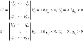 |
8 |
By averaging all the elements of matrices B+ and B–, we obtained the fractions of positive and negative g-factor areas, which, respectively, are 0.60 and 0.40. The area of the thin film studied is, thus, partitioned in 60% of positive and 40% negative g-factors domains. The slight imbalance between positive and negative sign domains ultimately affects the global g-factor value of +0.135, which is indeed positive.
After the evaluation of the spatial partition between domains characterized by opposite g-factor signs, we calculated the two actual g-factors coming out from the two domains’ group with opposite sign. We multiplied each element of B+ and B– (respectively, b+i,j and b–i,j) by the corresponding element of the g-factor matrix G (gi,j). The two obtained matrices G+ and G– are exclusively reporting g-factor values of the same sign within the matrix G, and all the other elements with opposite sign with respect to the one of interest are substituted with 0.
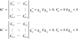 |
9 |
Afterward, we averaged all the nonzero elements of matrices G+ and G– to calculate the two overall opposite sign g-factors on the analyzed area of the material. For the positive g-factor domains, we obtained an emergent value of +0.585, while for the negative ones, an emergent value of −0.527 was obtained. This evidence suggests that the globally positive g-factor obtained is exclusively dominated by the ratio between positive and negative g-factor domains and the magnitude of each sign does not play a relevant role.
In other words, with reference to our previous papers,20,47 we can say that product 2 self-organizes in domains which are characterized by a |g-factor| around 0.55, but these domains prefer to lay 60:40 on the face providing positive apparent ECD.
3. Conclusions
With the aid of a standard optical microscope equipped with a digital camera and inexpensive optical elements, we evaluated the spatially resolved ECD of two thin film samples made by the organic chiral π-molecules 1 and 2. CPM images revealed marked differences between the ECD-homogeneous 1 thin film and the ECD-inhomogeneous (S,S)-PTPO 2 thin film. Despite the simplicity of the technique and its instrumental limitations in terms of sensitivity (actual limit of detection of 10–2 in optimal absorbance conditions), CPM allows for a quantitative evaluation of the spatially resolved ECD. For the film of 2, a spatial partition between domains characterized by equal and opposite ECD was highlighted, with a spatial resolution on the μm scale, which is smaller than the typical domains’ scale of π-conjugated materials in thin film. Through comparison between the ECD measured with a conventional spectropolarimeter (i.e., the spatially averaged ECD) and the spatially resolved ECD obtained with the microscope, we established that the overall positive emergent ECD signal of 2 thin film is solely dictated by the excess of domains with positive ECD on the surface. The possibility to employ a standard microscope and a simple experimental protocol to extract localized ECD data may prove useful in several fields ranging from materials science to biochemistry and biology.
Acknowledgments
This work was financially supported by the European Commission Research Executive Agency, Horizon 2020 Research, and Innovation Programme under the Marie Sklodowska-Curie grant agreement No. 859752-HEL4CHIROLED-H2020-MSCAITN-2019. The authors are grateful to Paolo Nardini, who realized a mount for holding optical elements of the microscope.
Supporting Information Available
The Supporting Information is available free of charge at https://pubs.acs.org/doi/10.1021/cbmi.3c00049.
Full experimental details, benchtop ECD characterization data of all compounds, and data processing images (PDF)
Author Contributions
A.T., F.Z., and L.D.B. designed the CPM setup, the experiments, and the analyses. A.T. prepared the samples, took CPM images, and ran numerical analyses. All data were discussed jointly with F.Z. and L.D.B. The results were critically analyzed by all coauthors in light of previous collaborations. A.T. drafted the manuscript, which was elaborated to its final form by all authors.
The authors declare no competing financial interest.
Supplementary Material
References
- Ostroverkhova O. Organic Optoelectronic Materials: Mechanisms and Applications. Chem. Rev. 2016, 116, 13279–13412. 10.1021/acs.chemrev.6b00127. [DOI] [PubMed] [Google Scholar]
- Brandt J. R.; Salerno F.; Fuchter M. J. The added value of small molecule chirality in technological applications. Nat. Chem. Rev. 2017, 1, 0045. 10.1038/s41570-017-0045. [DOI] [Google Scholar]
- Albano G.; Aronica L. A.; Minotto A.; Cacialli F.; Di Bari L. Chiral Oligothiophenes with Remarkable Circularly Polarized Luminescence and Electroluminescence in Thin Films. Chem.—Eur. J. 2020, 26, 16622–16627. 10.1002/chem.202003547. [DOI] [PubMed] [Google Scholar]
- Di Nuzzo D.; Kulkarni C.; Zhao B.; Smolinsky E.; Tassinari F.; Meskers S. C. J.; Naaman R.; Meijer E. W.; Friend R. H. High Circular Polarization of Electroluminescence Achieved via Self-Assembly of a Light-Emitting Chiral Conjugated Polymer into Multidomain Cholesteric Films. ACS Nano 2017, 11, 12713–12722. 10.1021/acsnano.7b07390. [DOI] [PubMed] [Google Scholar]
- Hutchins D. O.; Weidner T.; Baio J.; Polishak B.; Acton O.; Cernetic N.; Ma H.; Jen A. K.-Y. Effects of self-assembled monolayer structural order, surface homogeneity and surface energy on pentacene morphology and thin film transistor device performance. J. Mater. Chem. 2013, 1, 101–103. 10.1039/C2TC00378C. [DOI] [PMC free article] [PubMed] [Google Scholar]
- Albano G.; Pescitelli G.; Di Bari L. Chiroptical Properties in Thin Film of π-Conjugated Systems. Chem. Rev. 2020, 120 (18), 10145–10243. 10.1021/acs.chemrev.0c00195. [DOI] [PubMed] [Google Scholar]
- Wade J.; Salerno F.; Kilbride R. C.; Kim D. K.; Schmidt J. A.; Smith J. A.; LeBlanc L. M.; Wolpert E. H.; Adeleke A. A.; Johnson E. R.; Nelson J.; Mori T.; Jelfs K. E.; Heutz S.; Fuchter M. J. Controlling anisotropic properties by manipulating the orientation of chiral small molecules. Nat. Chem. 2022, 14, 1383–1389. 10.1038/s41557-022-01044-6. [DOI] [PubMed] [Google Scholar]
- Wan L.; Shi X.; Wade J.; Campbell A. J.; Fuchter M. J. Strongly Circularly Polarized Crystalline and β- Phase Emission from Poly(9,9-dioctylfluorene)-Based Deep-Blue Light-Emitting Diodes. Adv. Optical Mater. 2021, 9, 2100066. 10.1002/adom.202100066. [DOI] [Google Scholar]
- Korevaar P. A.; de Greef T. F.; Meijer E. W. Pathway Complexity in π-Conjugated Materials. Chem. Mater. 2014, 26, 576–586. 10.1021/cm4021172. [DOI] [Google Scholar]
- Schellman J. A. Circular Dichroism and Optical Rotation. Chem. Rev. 1975, 75 (3), 323–331. 10.1021/cr60295a004. [DOI] [Google Scholar]
- Stanchev S.; Rakovska R.; Berova N.; Snatzke G. Synthesis, Absolute Configuration and Circular Dichroism of Some Diarylmethane Derivatives. Tetrahedron 1995, 6 (1), 183–198. 10.1016/0957-4166(94)00374-K. [DOI] [Google Scholar]
- Wakai A.; Fukasawa H.; Yang C.; Mori T.; Inoue Y. Thoretical and Experimental Investigations of Circular Dichroism and Absolute Configuration Determination of Chiral Anthracene Photodimers. J. Am. Chem. Soc. 2012, 134, 4990–4997. 10.1021/ja300522y. [DOI] [PubMed] [Google Scholar]
- Politi M.; De Tommasi N.; Pescitelli G.; Di Bari L.; Morelli I.; Braca A. Structure and Absolute Configuration of New Diterpenes from Lavandula multifida. J. Nat. Prod. 2002, 65, 1742–1745. 10.1021/np020260p. [DOI] [PubMed] [Google Scholar]
- Pescitelli G.; Di Bari L.; Berova N. Conformational aspects in the studies of organic compounds by electronic circular dichroism. Chem. Soc. Rev. 2011, 40, 4603–4625. 10.1039/c1cs15036g. [DOI] [PubMed] [Google Scholar]
- Pescitelli G.; Di Bari L.; Berova N. Application of electronic circular dichroism in the study of supramolecular systems. Chem. Soc. Rev. 2014, 43, 5211. 10.1039/C4CS00104D. [DOI] [PubMed] [Google Scholar]
- Hempel J.; Schädle N.; Leptihn S.; Carle R.; Schweiggert R. M. Structure related aggragation behaviour of carotenoids and carotenoid esters. J. Photochem. Photobiol., A 2016, 317, 161–174. 10.1016/j.jphotochem.2015.10.024. [DOI] [Google Scholar]
- Kypr J.; Kejnovská I.; Renčiuk D.; Vorlíčková M. Circular dichroism and conformational polymorphism of DNA. Nucleic Acid Res. 2009, 37 (6), 1713–1725. 10.1093/nar/gkp026. [DOI] [PMC free article] [PubMed] [Google Scholar]
- Tian J.; Liu J.; He W.; Hu Z.; Yao X.; Chen X. Probing the Binding of Scutellarin to Human Serum Albumin by Circular Dichroism, Fluorescence Spectroscopy, FTIR, and Molecular Modeling Method. Biomacromolecules 2004, 5, 1956–1961. 10.1021/bm049668m. [DOI] [PubMed] [Google Scholar]
- Enamullah M.; Uddin A. K. M. R.; Pescitelli G.; Berardozzi R.; Makhloufi G.; Vasylyeva V.; Chamayou A.-C.; Janiak C. Induced chirality-at-metal and diastereoselectivity Δ/Λ-configured distorted square-planar copper complexes by enantiopure Schiff base ligands: combined circular dichroism, DFT and X-ray structural studies. Dalton Trans. 2014, 43, 3313–3329. 10.1039/C3DT52871E. [DOI] [PubMed] [Google Scholar]
- Albano G.; Salerno F.; Portus L.; Porzio W.; Aronica L. A.; Di Bari L. Outstanding Chiroptical Features of Thin Films of Chiral Oligothiophenes. ChemNanoMat 2018, 4, 1059–1070. 10.1002/cnma.201800244. [DOI] [Google Scholar]
- Yang Y.; Correa da Costa R.; Fuchter M. J.; Campbell A. J. Circularly polarized light detection by a chiral organic semiconductor transistor. Nature Photon 2013, 7, 634–638. 10.1038/nphoton.2013.176. [DOI] [Google Scholar]
- Hume P. A.; Monks J. P.; Pop F.; Davies E. S.; MacKenzie R. C. I.; Amabilino D. B. Self-Assembly of Chiral-at-End Diketopyrrolopyrroles: Symmetry Dependent Solution and Film Optical Activity and Photovoltaic Performance. Chem.—Eur. J. 2018, 24, 14461–14469. 10.1002/chem.201802610. [DOI] [PubMed] [Google Scholar]
- Huang X.; Li C.; Jiang S.; Wang X.; Zhang B.; Liu M. Self-Assembled Spiral Nanoarchitecture and Supramolecular Chirality in Langmuir-Blodgett Films of an Achiral Amphiphilic Barbituric Acid. J. Am. Chem. Soc. 2004, 126, 1322–1323. 10.1021/ja036878i. [DOI] [PubMed] [Google Scholar]
- Maestre M. F.; Katz J. E. A Circular Dichroism Microspectrophotometer. Biopolymers 1982, 21, 1899–1908. 10.1002/bip.360210916. [DOI] [Google Scholar]
- Zinna F.; Resta C.; Górecki M.; Pescitelli G.; Di Bari L.; Jávorfi T.; Hussain R.; Siligardi G. Circular Dichroism Imaging: Mapping the Local Supramolecular Order in Thin Films of Chiral Functional Polymers. Macromolecules 2017, 50, 2054–2060. 10.1021/acs.macromol.6b02590. [DOI] [Google Scholar]
- Albano G.; Górecki M.; Pescitelli G.; Di Bari L.; Jávorfi T.; Hussain R.; Siligardi G. Electronic circular dichroism imaging (CDi) maps local aggregation modes in thin films of chiral oligothiophenes. New J. Chem. 2019, 43, 14584–14593. 10.1039/C9NJ02746G. [DOI] [Google Scholar]
- Albano G.; Górecki M.; Jávorfi T.; Hussain R.; Siligardi G.; Pescitelli G.; Di Bari L. Spatially resolved chiroptical study of benzo[1,2-b:4,5-b’]dithiophene-based oligothiophenes by synchrotron radiation electronic circular dichroism imaging (SR-ECDi) technique. Aggregate 2022, 3, 193. 10.1002/agt2.193. [DOI] [Google Scholar]
- Hussain R.; Jávorfi T.; Siligardi G. CD Imaging at High Spatial Resolution at Diamond B23 Beamline: Evolution and Applications. Front. Chem. 2021, 9, 616928. 10.3389/fchem.2021.616928. [DOI] [PMC free article] [PubMed] [Google Scholar]
- Narushima T.; Okamoto H. Circular dichroism nano-imaging of two-dimensional chiral metal nanostructures. Phys. Chem. Chem. Phys. 2013, 15, 13805. 10.1039/c3cp50854d. [DOI] [PubMed] [Google Scholar]
- Narushima T.; Okamoto H. Strong Nanoscale Optical Activity Localized in Two-Dimensional Chiral Metal Nanostructures. J. Phys. Chem. C 2013, 117, 23964–23969. 10.1021/jp409072h. [DOI] [PubMed] [Google Scholar]
- Hashiyada S.; Narushima T.; Okamoto H. Local Optical Activity in Achiral Two.Dimensional Gold Nanostructures. J. Phys. Chem. C 2014, 118, 22229–22233. 10.1021/jp507168a. [DOI] [Google Scholar]
- Drake A. F. Polarisation modulation-the measurement of linear and circular dichroism.hue. J. Phys. E: Sci. Instrum. 1986, 19, 170–181. 10.1088/0022-3735/19/3/002. [DOI] [Google Scholar]
- Shindo Y.; Ohmi Y. Problems of CD spectrometers. 3. Critical comments on liquid crystal induced circular dichroism. J. Am. Chem. Soc. 1985, 107, 91–97. 10.1021/ja00287a017. [DOI] [Google Scholar]
- Shindo Y.; Nakagawa M. Circular dichroism measurements. I. Calibration of a circular dichroism spectrometer. Rev. Sci. Instrum. 1985, 56, 32–39. 10.1063/1.1138467. [DOI] [Google Scholar]
- Narushima T.; Okamoto H. Circular Dichroism Microscopy Free from Commingling Linear Dichroism via Descretely Modulated Circular Polarization. Sci. Rep. 2016, 6, 35731. 10.1038/srep35731. [DOI] [PMC free article] [PubMed] [Google Scholar]
- Szustakiewicz P.; Kowalska N.; Grzelak D.; Narushima T.; Góra M.; Bagiński M.; Pociecha D.; Okamoto H.; Liz-Marzán L. M.; Lewandowaski W. Supramolecular Chirality Synchronization in Thin Films of Plasmonic Nanocomposites. ACS Nano 2020, 14, 12918–12928. 10.1021/acsnano.0c03964. [DOI] [PMC free article] [PubMed] [Google Scholar]
- Nakajima R.; Hirobe D.; Kawaguchi G.; Nabei Y.; Sato T.; Narushima T.; Okamoto H.; Yamamoto H. M. Giant spin polarization and a pair of antiparallel spins in a chiral superconductor. Nature 2023, 613, 479–484. 10.1038/s41586-022-05589-x. [DOI] [PubMed] [Google Scholar]
- Jensen H. P.; Schellman J. A.; Troxell T. Modulation Techniques in Polarization Spectroscopy. Appl. Spectrosc. 1978, 32, 192–200. 10.1366/000370278774331567. [DOI] [Google Scholar]
- Shindo Y.; Nakagawa M.; Ohmi Y. On the Problems of CD Spectropolarimeters. II: Artifacts in CD Spectrometers. Appl. Spectrosc. 1985, 39, 860–868. 10.1366/0003702854250022. [DOI] [Google Scholar]
- Arteaga O.; Freudenthal J.; Wang B.; Kahr B. Mueller matrix polarimetry with four photoelastic modulators: theory and calibration. Appl. Opt. 2012, 51 (28), 6805–6817. 10.1364/AO.51.006805. [DOI] [PubMed] [Google Scholar]
- Claborn K.; Puklin-Faucher E.; Kurimoto M.; Kaminsky W.; Kahr B. Enantiomorphous twinning in biaxial crystals of 1,8-Dihydroxyanthraquinone. J. Am. Chem. Soc. 2003, 125, 14825–14831. 10.1021/ja035644w. [DOI] [PubMed] [Google Scholar]
- Frawley A. T.; Pal R.; Parker D. Very bright, enantiopure europium(III) complexes allow time-gated chiral contrast imaging. Chem. Commun. 2016, 52, 13349–13352. 10.1039/C6CC07313A. [DOI] [PubMed] [Google Scholar]
- Kitagawa Y.; Wada S.; Islam M. D. J.; Saita K.; Gon K.; Fushimi K.; Tanaka K.; Maeda S.; Hasegawa Y. Chiral lanthanide lumino-glass for a circularly polarized light security device. Commun. Chem. 2020, 3, 119. 10.1038/s42004-020-00366-1. [DOI] [PMC free article] [PubMed] [Google Scholar]
- Stachelek P.; MacKenzie L.; Parker D.; Pal R. Circularly polarised luminescence laser scanning confocal microscopy to study live cell chiral molecular interactions. Nat. Commun. 2022, 13, 553. 10.1038/s41467-022-28220-z. [DOI] [PMC free article] [PubMed] [Google Scholar]
- De Rosa D. F.; Stachelek P.; Black D. J.; Pal R. Rapid handheld time-resolved circularly polarised luminescence photography camera for life and material sciences. Nat. Commun. 2023, 14, 1537. 10.1038/s41467-023-37329-8. [DOI] [PMC free article] [PubMed] [Google Scholar]
- Yang Y.; Correa da Costa R.; Smilgies D.-M.; Campbell A. J.; Fuchter M. J. Induction of Circularly Polarized Electroluminescence from an Achiral Light-Emitting Polymer via a Chiral Small-Molecule Dopant. Adv. Mater. 2013, 25, 2624–2628. 10.1002/adma.201204961. [DOI] [PMC free article] [PubMed] [Google Scholar]
- Zinna F.; Albano G.; Taddeucci A.; Colli T.; Aronica L. A.; Pescitelli G.; Di Bari L. Emergent Nonreciprocal Circularly Polarized Emission fron an Organic Thin Film. Adv. Mater. 2020, 32, 2002575. 10.1002/adma.202002575. [DOI] [PubMed] [Google Scholar]
- Albano G.; Lissia M.; Pescitelli G.; Aronica L. A.; Di Bari L. Chiroptical response inversion upon sample flipping in thin films of a chiral benzo[1,2-b:4,5-b’]-dithiophene-based oligothiophene. Mater. Chem. Front. 2017, 1, 2047–2056. 10.1039/C7QM00233E. [DOI] [Google Scholar]
- Zinna F.; Pescitelli G.; Di Bari L. Circularly polarized light at the mirror: Caveats and opportunities. Chirality 2020, 32, 765–769. 10.1002/chir.23217. [DOI] [PubMed] [Google Scholar]
- Salij A. H.; Goldsmith R. H.; Tempelaar R.. Chiral polaritons based on achiral Fabry-Perot cavities using apparent circular dichroism. arXiv 2022, arXiv:2208.14461. [DOI] [PMC free article] [PubMed] [Google Scholar]
- Shindo Y. Application of polarized modulation technique in polymer science. Opt. Eng. 1995, 34, 3369–3384. 10.1117/12.213252. [DOI] [Google Scholar]
- Kuroda R.; Harada T.; Shindo Y. A solid-state dedicated circular dichroism spectrophotometer: Development and application. Rev. Sci. Instrum. 2001, 72, 3802–3810. 10.1063/1.1400157. [DOI] [Google Scholar]
- Salij A.; Goldsmith R. H.; Tempelaar R. Theory of Apparent Circular Dichroism Reveals the Origin of Inverted and Noninverted Chiroptical Response under Sample Flipping. J. Am. Chem. Soc. 2021, 143, 21519–21531. 10.1021/jacs.1c06752. [DOI] [PubMed] [Google Scholar]
- Berova N., Nakanishi K., Woody R. W., Eds. Circular Dichroism: Principles and Applications, 2nd ed.; Wiley-VCH: New York, 2000. [Google Scholar]
- Goodstein R. L., Ed. Boolean Algebra; Dover Publications: New York, 2012. [Google Scholar]
Associated Data
This section collects any data citations, data availability statements, or supplementary materials included in this article.


