Abstract
Na1/2Eu1/2Cu3Ti4O12 and Na1/2Sm1/2Cu3Ti4O12 dielectric ceramics were synthesized at different sintering temperatures (950, 975 and 1000 °C) by a solid-state reaction method. Phase structure, cation valence state, and dielectric properties of all sintered ceramics were systematically investigated. When the preparation temperature was changed, the Cu+ ion concentration of (Na+, Eu3+) co-doped ceramics changed faster than that of (Na+, Sm3+) co-doped ceramics. Abnormally high dielectric constants of ~ 3.17 × 10⁴ and ~ 1.06 × 10⁴ (at 10 Hz and 303 K) were achieved in Na1/2Sm1/2Cu3Ti4O12 and Na1/2Eu1/2Cu3Ti4O12 ceramics prepared at 950 °C, respectively. However, Na1/2Sm1/2Cu3Ti4O12 and Na1/2Eu1/2Cu3Ti4O12 prepared in high sintering temperature (1000 °C) exhibited a good frequency stability of dielectric permittivity. It was demonstrated that an increasing number of charge carriers induced by the increase of sintering temperature could lead to a competitive coexistence of two polarization mechanisms (surface barrier layer capacitor and internal barrier layer capacitor), further changing the dielectric properties of CaCu3Ti4O12-based ceramics.
Subject terms: Ceramics, Solid-state chemistry
Introduction
With the rapid development of network and information technology, the fifth generation (5G) network, online classroom and other technologies that are inseparable from people’s lives are increasingly demanding the performance of capacitors, the basic components of electronic products1–3. Therefore, the research on the dielectric properties of different dielectric materials has always been a hot issue4–7. As a traditional dielectric material, CaCu3Ti4O12 (CCTO) has been closely watched since its giant dielectric properties were found8–11. Two major aspects ways are used to optimize the dielectric properties of CCTO-like ceramics: (1) use of different preparation methods, for instance, solid-state reaction method12, sol–gel13, and spark plasma sintering14, (2) the substitution of ions in the lattice, like La2O315, Y2/3Cu3Ti4O1216,Mg0.05Al0.0517, Na1/2Y1/2Cu3Ti4O1218, Na1/2La1/2Cu3Ti4O1219, Ca1-xSrxCu3Ti4O12-xFx20 and Na1/3Yb1/3Ca1/3Cu3Ti4O1221, etc. Simultaneously, internal barrier layer capacitors (IBLC), as a major polarization mechanism, is used to explain the origin of dielectric behaviors for CCTO-based family materials22,23.
The IBLC model is considered to be an internal capacitor composed of semiconductor grains surrounded by insulating grain boundaries, which has also been discovered in other dielectric materials, such as the BaTiO3− type ceramics24 and rutile TiO2-related ceramics25,26. Among them, the conductivity level of grain and grain boundary plays an important role in IBLC effect, which is affected by the number of charge carriers in the ceramic. For example, a high dielectric constant and a low loss tangent observed in Na1/3Ca1/3Bi1/3Cu3Ti4O12 has been attributed to the electrically heterogeneous and comprised of semiconducting grains and insulating grain boundaries, while the semiconducting grains is primarily due to electron hopping between Cu+ ↔ Cu2+ and Ti3+ ↔ Ti4+ sites27. The colossal dielectric of Na1/2Y1/2Cu3Ti4O12 ceramic are closely related to the electrically heterogeneous microstructure at the insulating grain boundary, and the origin of semiconducting grains is likely correlated with the Cu2O phase and the large amount of Ti3+/Ti4+ ions28. For (Al3+,Nb5+) co-doped CaCu3Ti4O12 ceramics, the high dielectric permittivities with good temperature stability has been attributed to the internal barrier layer capacitor model of Schottky barriers at grain boundaries, meanwhile electron hopping can occur in both Ti3+–O–Ti4+ and Cu+–O–Cu2+ ions29.
It is obvious that the dielectric properties of CCTO-related ceramics can be effectively improved by the doping of ions, especially multiple cations (shown in the Table 1). But few reports explained the relationship between the preparation conditions (especially sintering temperature), grain conductivity, internal polarization mechanism, and dielectric properties of ceramics. Thus, it is fundamentally important to build a clear picture for the evolution of internal polarization mechanism along with the number of charge carriers in grain. Up to the present time, little work has been done on the sintering temperature, structural and dielectric properties of the signal phase (Na+, Eu3+) or (Na+, Sm3+) co-doped CCTO ceramics, specifically Na1/2Eu1/2Cu3Ti4O12 and Na1/2Sm1/2Cu3Ti4O12. Boonlakhorn et al. and Somphan et al. reported the good dielectric properties of Na1/2Sm1/2Cu3Ti4O12 ceramics respectively, but a little impurity phase of Sm4Ti3O12 or CuO was detected in ceramics31,32. Considering the comparison with Sm doped ACu3Ti4O12 ceramics, the Eu ion closest to Sm in the periodic table of the elements was selected as doping ion to study the polarization mechanism and dielectric properties for CCTO-related ceramics. And, there is no discussion on the relationship between sintering temperature, the number of charge carriers, polarization mechanism and dielectric properties of Na1/2Eu1/2Cu3Ti4O12 and Na1/2Sm1/2Cu3Ti4O12 ceramics. A better understanding of the effect of polarization mechanism could be helpful for designing oxide ceramics with superior dielectric properties.
Table 1.
Sintering process, mean grain size and dielectric properties of some LnCu3Ti4O12 (Ln = Na1/2Bi1/2, Na1/2Sm1/2, Na1/2Eu1/2, Na1/2La1/2, Na1/2Y1/2, Na1/3Ca1/3Bi1/3 and Na1/3Ca1/3Yb1/3 etc.) ceramics.
| Samples | Preparation method | Sintering conditions | Mean grain size (μm) | Dielectric constant (1 kHz) | Dielectric loss (1 kHz) | References |
|---|---|---|---|---|---|---|
| Bi1/2Na1/2Cu3Ti4O12 | Pechini method | 1000 °C for 10 h | 3.2 | 2.77 × 10³ | 0.11 | 30 |
| Na1/2Bi1/2Cu3Ti4O12 | Sol–gel | 1000 °C for 3 h | 2.2 | ≈ 104 | – | 9 |
| Na1/3Ca1/3Bi1/3Cu3Ti4O12 | Solid state method | 1060 °C for 5 h | 2–20 | 2.59 × 10⁴ | 0.038 | 27 |
| Na1/2Sm1/2Cu3Ti4O12 | Sol–gel | 1050 °C for 18 h | 3.67 | 8.04 × 10³ | 0.045 | 31 |
| Na1/2Sm1/2Cu3Ti4O12 | Solid state method | 1110 °C for 10 h | – | 7.02 × 10³ | 0.041 | 32 |
| Na1/2La1/2Cu3Ti4O12 | Solid state method | 1080 °C for 5 h | 2–4 | 6.1 × 10³ | 0.037 | 33 |
| Na1/2La1/2Cu3Ti4O12 | Spark plasma sintering | 925 °C for 10 min | 0.3 | > 103 | – | 14 |
| Na1/2Y1/2Cu3Ti4O12 | Solid state method | 1085 °C for 5 h | 11 | 1.4 × 10⁴ | 0.04 | 18 |
| Na1/2Y1/2Cu3Ti4O12 | Solid state method | 1110 °C for 10 h | 10.32 | 1.8 × 10⁴ | 0.03 | 28 |
| Na1/2Y1/2Cu3Ti4.1O12 | Solid state method | 1090 °C for 5 h | 4.06 | 2.56 × 10⁴ | 0.022 | 8 |
| (Na1/3Ca1/3Yb1/3)Cu3Ti4O12 | Sol–gel | 1075 °C for 12 h | 0.18–0.4 | 5488 | 0.075 | 21 |
| Na1/2Sm1/2Cu3Ti4O12 | Solid state method | 1000 °C for 10 h | 19.73 | 5.5 × 10³ | 0.055 | This work |
| Na1/2Eu1/2Cu3Ti4O12 | Solid state method | 1000 °C for 10 h | 16.9 | 4.7 × 10³ | 0.066 | This work |
In this study, the Na1/2Ln1/2Cu3Ti4O12 (Ln = Eu or Sm) ceramics were synthesized by solid-state reaction. The relationship among microstructure, polarization mechanism and dielectric properties of Na1/2Ln1/2Cu3Ti4O12 (Ln = Eu or Sm) ceramics had been conformed for the first time by carefully tuning the number of charge carriers in grain via the change of sintering temperature. It could be notable that the sintering temperature altered the number of charge carriers in grain, induce different polarization mechanism, resulting in varied dielectric properties of the Na1/2Ln1/2Cu3Ti4O12 ceramics.
Materials and methods
Sample preparation
Na1/2Eu1/2Cu3Ti4O12 and Na1/2Sm1/2Cu3Ti4O12 ceramics were prepared via a solid state reaction method. The raw materials, TiO2 (99.99%), CuO (99.95%), CaCO3 (99.9%), Eu2O3 (99.9%) and Sm2O3 (99.9%) were carefully weighed and milled. First, the green pellets obtained with a uniaxial press were calcined at 600 °C for 10 h in air. The calcined pellets were ground into powders, and the obtained powders were pressed into pellets again. Then, the ceramic samples were obtained by sintering compacted powder at different temperatures from 950 to 1000 °C for 10 h. For clarity, the obtained ceramics are named based on the composition (Na1/2X1/2Cu3Ti4O12 expressed as NXCTO), and the sintering temperature (T in °C) as NXCTO-T. For example, the Na1/2Eu1/2Cu3Ti4O12 ceramic sintered at 950 °C is named as NECTO-950.
Characterization
Crystal structure of these samples characterized using Powder X-ray diffraction (XRD) with a D8-focu Bruker apparatus (Cu Kα, λ = 0.15418 nm). The structural study was further performed by Raman spectra (RS) using a T64000 instrument under a 532 nm laser beam. The microstructural texture, and oxidation states were also analyzed by canning electron microscope (SEM) (FEI XL-30, America) and X-ray photoelectron spectroscopy (XPS, Escalab 250XI), respectively. The C1s photoemission line (284.6 eV) was used to calibrate the positions of the photoelectron spectra.
All pellets were carefully polished, and then coated surfaces with an Au layer film using a LJ-16 sputter coating unit. The dielectric properties of the ceramics were measured using a dielectric spectrometer (Novocontrol Concept 41) over the frequency and temperature ranges of 10 to 2 ⨯ 107 Hz and − 70 to 200 °C.
Results and discussion
X-ray diffraction analysis
Sintered Na1/2Eu1/2Cu3Ti4O12 and Na1/2Sm1/2Cu3Ti4O12 ceramics were first characterized using an XRD technique to confirm its phase structures. Figure 1a demonstrates the XRD patterns of the NECTO and NSCTO ceramics sintered under various temperatures from 950 to 1000 °C. A main phase of CaCu3Ti4O12 (JCPDS 75-2188) with a cubic structure was defected in all ceramic samples. No impurity phase was observed. As shown in the Fig. 1b, the (220) peak shifts to a lower degree with increasing sintered temperature in the NECTO and NSCTO samples. The relevant lattice parameters, a, were calculated from the XRD patterns. The a values of the CaCu3Ti4O12 was 7.391 Å21. The a values of the NECTO and NSCTO ceramics sintered at 950 °C were respectively found to be 7.379 and 7.381 Å, respectively. The lattice parameters (a) of NECCTO-950 and NSCCTO-975 were slightly smaller than that of CaCu3Ti4O12, which was due to the small difference in the ionic radii in Na+ ( = 1.39 Å), Sm3+ ( = 1.24 Å), Eu3+ ( = 1.12 Å) and Ca2+ ( = 1.34 Å).
Figure 1.
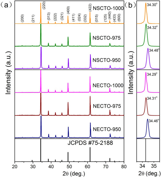
(a) XRD patterns of Na1/2Eu1/2Cu3Ti4O12 and Na1/2Sm1/2Cu3Ti4O12 ceramics sintered under different temperature; (b) changes of (220) diffraction peaks of these ceramic samples.
Although the radius of Na+ ion is larger than that of Ca2+, the lattice of NECCTO-950 and NSCCTO-950 sample shrined with the occupation of Sm3+ and Eu3+ ions with a smaller radius in the CCTO-type structure. The a values of the NECTO and NSCTO samples sintered at 975 and 1000 °C were 7.388, 7.399 and 7.387, 7.392 Å, respectively. Interestingly, a values of the NECTO and NSCTO samples sintered at high temperature were significantly larger than that of ceramics prepared at low temperature, which could be attributed to the change in the cation valence state in the rutile crystal structure.
Raman spectrogram analysis
Raman spectra of NECTO and NSCTO pellets sintered at different temperature are depicted in Fig. 2a,b. In Fig. 2, five modes at around 153, 358, 450 and 552 cm−1 were observed for six ceramics, in agreement with previous reports10. The Raman active modes of NECTO and NSCTO ceramics, like CaCu3Ti4O12, could be similarly expressed as ΓRaman = 2Ag + 2Eg + 4Fg34. These Raman modes corresponded to Fg (1), Ag (1), Ag (2) and Fg (3), respectively. Among these modes, the Ag (1), Ag (2) and Fg (1) modes was attributed to TiO6 rotation like lattice vibrations, and the Fg (3) mode was associated with an O–Ti–O antistretching lattice vibrations.
Figure 2.
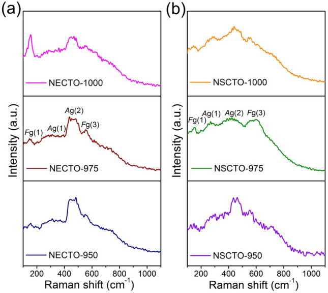
Raman spectra of (a) Na1/2Eu1/2Cu3Ti4O12 and (b) Na1/2Sm1/2Cu3Ti4O12 ceramics samples prepared in different sintering temperatures.
Microstructure
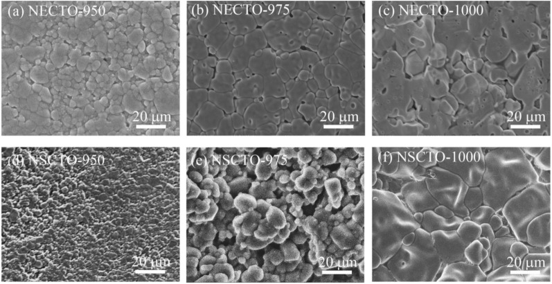
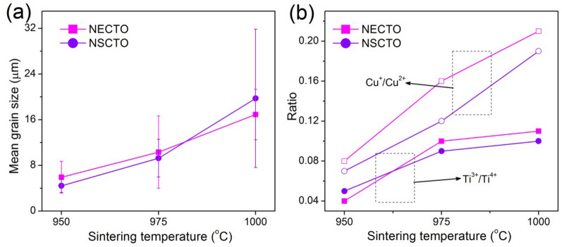
The microstructures of the NECTO-950, NECTO-975, NECTO-1000, NSCTO-950, NSCTO-975 and NSCTO-1000 are shown in Fig. 3a–f, respectively. The mean grain size of all the ceramics are revealed in Fig. 4a. Figure 3 shows that all the ceramic samples had a relatively dense microstructure. Grains and grain boundaries were clearly observed. However, a very small amount of pores appeared on the microscopic surface for the ceramic samples sintered in the low temperature (e.g. NECTO-950, NECTO-975, NSCTO-950 and NSCTO-975). To study the microscopic surface for the NECTO and NSCTO ceramics sintered at different temperature, as shown in Fig. 4a, it was found that the sintering temperature had a significant influence on the microstructure. The results showed that the mean grain size of Na1/2Eu1/2Cu3Ti4O12 samples prepared at various temperature increased slightly as the sintering temperature increased from 950 to 1000 °C, ≈ 5.93, ≈ 11.32, ≈ 16.9 μm, respectively. Similarly, the mean grain size of NSCTO ceramics also increased with the increase of sintering temperature. The change in the grain size of the ceramics is usually associated with the liquid phase sintering mechanism, as reported in other CCTO-related ceramics30,35–37. However, in case of the NSCTO ceramics, the microstructure largely changed when the sintering temperature changed by only 25 °C. This phenomenon was similar to the Na1/2Ln1/2Cu3Ti4O12-type ceramics reported by other researchers (shown in the Table 1). When the doping elements of Na1/2Ln1/2Cu3Ti4O12-type ceramics changed from Y, La, Sm, Yb to Bi, the grain size of the prepared ceramics also showed significant changes. It may be related to the state of the extranuclear electron of the element. The Sm element is one atomic number lower than the Eu element, and the electrons of the 4f electron orbit are also one less, which may result in different grain growth trends of the NSCTO and NECTO ceramics under the same preparation conditions. The density of the samples has been measured by Archimedes method. As sintering temperature increased, the relative density of the NECTO ceramics increased monotonically from 83% for T = 950 °C and 87% for T = 975 °C to 91% for T = 1000 °C. And the relative density of NSCTO ceramics also increased with sintering temperature, reaching 81%, 85% and 92%, respectively.
Figure 3.
SEM images of Na1/2Eu1/2Cu3Ti4O12 and Na1/2Sm1/2Cu3Ti4O12 ceramics sintered under various temperature: (a) NECTO-950, (b) NECTO-975, (c) NECTO-1000, (d) NSCTO-950, (e) NSCTO-975 and (f) NSCTO-1000.
Figure 4.
(a) Curves of mean grain size vs. sintering temperature for Na1/2Eu1/2Cu3Ti4O12 and Na1/2Sm1/2Cu3Ti4O12 ceramics. (b) Relationship between the atomic ratio of Cu+/Cu2+ or Ti3+/Ti4+ and sintering temperature for these samples. Solid dots and hollow dots in (b) correspond to the ratio of Ti3+/Ti4+ and the ratio of Cu+/Cu2+, respectively.
XPS analysis
To identify the oxidation states of the polyvalent cations, the XPS spectrum was corrected. Figures 5 and 6 displayed the spectra of Ti 2p, Cu 2p for NECTO and NSCTO ceramics sintered at different temperature. Meanwhile, atomic ratios of Cu+/Cu2+ and Ti3+/ Ti4+ estimated by XPS analysis were shown in the Fig. 4b in order to study the change of variable valence ion content in these ceramic samples. As presented in Fig. 5, two asymmetrically shaped Ti 2p3/2 and Ti 2p1/2 are observed, indicating overlapping peaks of Ti3+ and Ti4+ ions30,33,38. According to the Gaussian–Lorentzian profile fitting, four peaks were obtained as displayed in the Fig. 5. This was observed in all sintered ceramics. For the intensive peak Ti 2p3/2 of NECTO and NSCTO ceramics, binding energy positions defining Ti3+ and Ti4+ were ~ 456.55–456.98 eV and ~ 457.62–457.96 eV, respectively. Figure 4b shows the radios of Cu+/Cu2+ or Ti3+/Ti4+ for NECTO and NSCTO ceramics. It was clearly that the content of Ti3+ ions in NECTO and NSCTO ceramics sintered in low temperature (950 °C) maintained a minor amount, and it increased slightly with the increase of sintering temperature.
Figure 5.
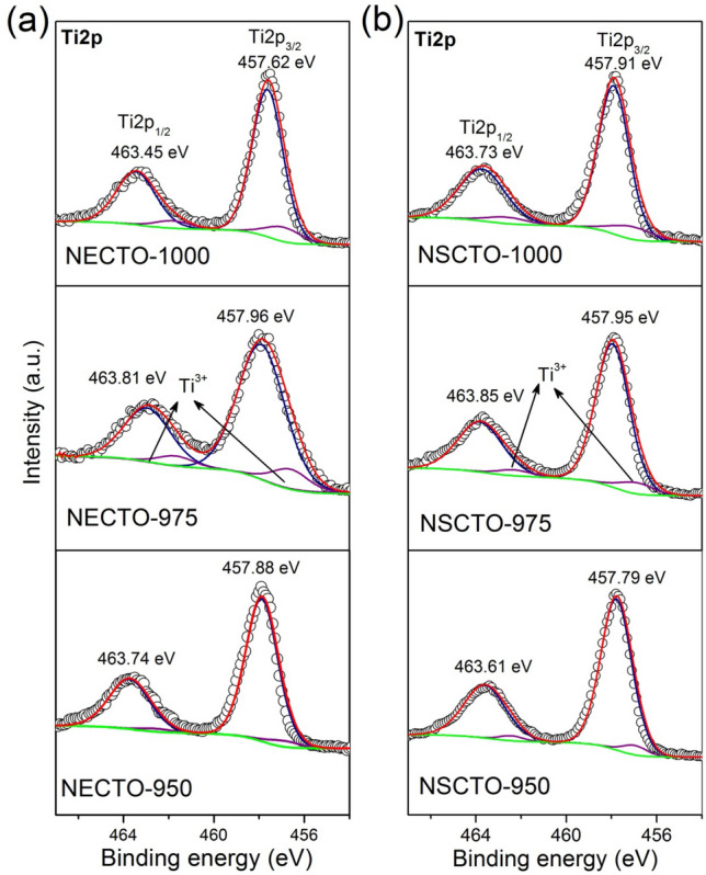
XPS spectra for the Ti 2p region for the (a) Na1/2Eu1/2Cu3Ti4O12 and (b) Na1/2Sm1/2Cu3Ti4O12 ceramics prepared at different sintering temperature.
Figure 6.
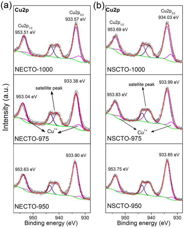
XPS spectra for the Cu 2p region for the (a) Na1/2Eu1/2Cu3Ti4O12 and (b) Na1/2Sm1/2Cu3Ti4O12 ceramics prepared at different sintering temperature.
Simultaneously, the Cu 2p spectrum in Fig. 6 indicate the presence of Cu+. The main signal corresponding to Cu 2p3/2 of all ceramic samples could be deconvoluted into two signals: the binding energy positions of Cu+ and Cu2+ are ~ 932.1–932.56 eV and ~ 933.38–934.03 eV, respectively. That is similar to that reported in the literature for CCTO and TiO2-related ceramics16,39,40. The appearance of Ti3+ and Cu+ detected in Na1/2Eu1/2Cu3Ti4O12 and Na1/2Sm1/2Cu3Ti4O12 ceramics might have been related to the charge compensation caused by oxygen loss in its lattice structure during the sintering process5,41. As shown in the Fig. 4b, the concentration of Cu+ in NECTO and NSCTO ceramics samples significantly increased with the rise of sintering temperature, which was different from that of Ti3+ in these ceramics.
Simultaneously, it could be clearly confirmed that the content of Cu+ in (Na+, Eu3+) co-doped CCTO ceramics was generally higher than that in (Na+, Sm3+) co-doped CCTO ceramics for calcium copper titanate related ceramics, which may be related to the different electronic structures of Eu and Sm elements. Obviously, the ionic radius of the low valence state was larger than it of the high valence state. Therefore, the lattice structure of ceramics expands and the lattice parameters increase with the reduction of Cu2+ and Ti4+ in the grains. The NECTO-1000 and NSCTO-1000 samples with high concentration of Cu+ ions had the higher lattice parameters than other ceramics samples, which corresponded to the results observed by XRD.
Dielectric properties
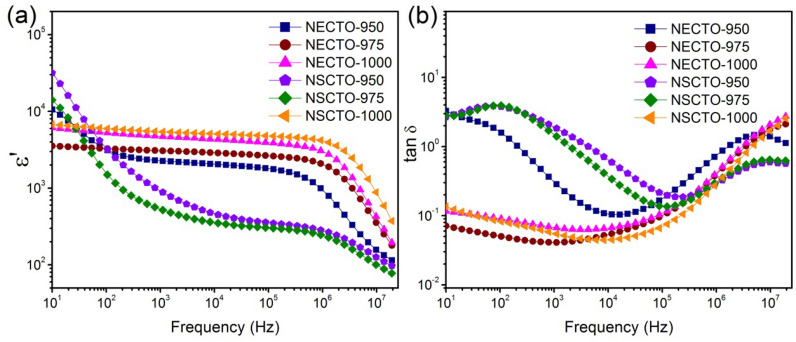
In order to comprehend how the sintering temperature and mixing ions affects the dielectric responses, frequency dependences of dielectric constant (ε′) and dielectric loss (tan δ) for all samples at room temperature are shown in Fig. 7. Clearly, the overall frequency dependent behaviors of the NECTO and NSCTO ceramics differed obviously. As shown in Fig. 7a, ε′ of NSCCTO-950 sample rapidly decreased from 16,116 to 881 as frequency increased in the low frequency region. This is similar to that observed in NECTO-950 and NSCTO-975 ceramics also prepared at low sintering temperature. However, the permittivity was nearly independent of frequency from 10 to 106 Hz for NECTO-975, NECTO-1000 and NSCTO-1000 samples. Notably, the frequency stabilities of ε′ for NECTO-1000 and NSCTO-1000 samples were better than that of the NECTO-975 sample. The drastic decrease of dielectric constants for these samples at high frequency (> 106 Hz) could be attributed to the interfacial space charge polarization16. Figure 7b shows that the tan δ value of the NECTO-975, NECTO-1000 and NSCTO-1000 ceramics in the low frequency were obviously smaller than that of the NECTO-950, NSCTO-950 and NSCTO-975 ceramics. The peaks of dielectric loss (tan δ) for NECTO-950, NSCTO-950 and NSCTO-975 ceramics are presented at low frequencies. The tan δ values at 303 K and 1 kHz of the NECTO-950, NECTO-975, NECTO-1000, NSCTO-950, NSCTO-975 and NSCTO-1100 ceramics were approximately 0.285, 0.041, 0.066, 1.841, 1.407 and 0.055, respectively. Notably, When (Na+, Eu3+) or (Na+, Sm3+) was co-doped in CCTO-related ceramic prepared at high sintering temperature (975 or 1000 °C), the ceramic could retain low tan δ value and giant permittivity with good frequency stability.
Figure 7.
(a) Dielectric constant (ε′) and (b) dielectric loss (tan δ) at 303 K as a function of frequency for Na1/2Eu1/2Cu3Ti4O12 and Na1/2Sm1/2Cu3Ti4O12 ceramics sintered at different temperature.
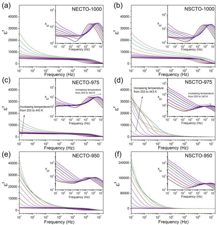
The frequency of real part ε′ and imaginary part ε″ for NECTO and NSCTO ceramics at different temperature were shown in the Fig. 8 and its insets. Three plateau characteristics in the plots of ε′ versus frequency were observed in the temperature range from 203 to 443 K, which corresponded to three main parts of dielectric responses, respectively. The first plateau in a low frequency range was observed at the high temperature, which is attributed to an sample-electrode interface response21,36. In the low frequency region, as the test temperature increased, the dielectric constant changed more sharply with frequency, indicating that the sample-electrode interface response, i.e. the surface barrier layer capacitor (SBLC) polarization mechanism, was more obvious. Therefore, as shown in Fig. 8, there was a strong SBLC effect inside the NECTO-950, NECTO-975 and NSCTO-950 ceramics prepared at low sintering temperature, which leads to the abnormal high dielectric constant of these ceramics in the low-frequency region (shown in the Fig. 7a). As the Fig. 7b, the dielectric loss peaks of these three ceramics observed at low frequencies were also related to the SBLC effect. The primary plateau observed at intermediate frequency was attributed to the dielectric response of the grain boundaries27,42, which was evident in the NECTO-1000, NSCTO-1000, and NECTO-975 ceramics prepared at high sintering temperature. However, the high frequency plateau observed at the low testing temperature was originated from the bulk response23. The dielectric responses of these three parts were clearly observed in CCTO-related ceramics27,42,43. As shown in the Fig. 8 insets, the peak of ε″ shifted to higher frequencies with increasing temperature, indicating that the dielectric relaxation process was thermally activated. It was found that the high frequency relaxation activation energies of the NECTO-950, NECTO-975, NECTO-1000, NSCTO-950, NSCTO-975, NSCTO-1000 ceramics were 0.116, 0.106, 0.102, 0.114, 0.113 and 0.100 eV, respectively. These activation energies were related to the electric response of the bulks or grains, which were similar to other CCTO-like ceramics44–46.
Figure 8.
Frequency dependence of ε′ at various temperatures for (a) NECTO-1000, (b) NSCTO-1000, (c) NECTO-975, (d) NSCTO-975, (e) NECTO-950 and (f) NSCTO-950; their insets show the frequency dependence of ε″ in a temperature range from 203 to 343 K.
Impedance spectroscopy analysis
To describe the dielectric behaviors of these ceramics, the impedance spectroscopy for NECTO and NSCTO ceramics was employed to illuminate this. In Fig. 9 and its inset, the linear part of the semicircular arcs with nonzero intercept on the Z′ axis was observed at 283 K. However, the semicircular arcs became apparent in low frequency region for NECTO-950, NSCTO-950 and NSCTO-975 ceramics (Fig. 9). For, CCTO-related ceramics, these electrical response are associated with the contributions from grain boundaries and grains, respectively47.
Figure 9.
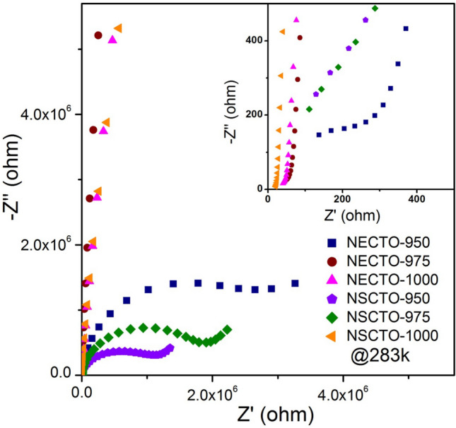
Impedance complex plane (Z*) plot at 283 K for Na1/2Eu1/2Cu3Ti4O12 and Na1/2Sm1/2Cu3Ti4O12 ceramics with different sintering temperature. Inset shows an expanded view of the Z* plot at 283 K in high frequency range.
The resistance values of grain, grain boundary and surface for NECTO and NSCTO ceramics were estimated using the equivalent R(RQ) circuit23 shown in Table 2. As displayed in the Table 2, the grain resistance (Rg) values of these Na1/2Ln1/2Cu3Ti4O12 (Ln = Eu or Sm) ceramics evidently decreased with increasing sintering temperature. The variation of Rg values for these ceramics was related to the appearance of low valent ions (Cu+ and Ti3+) at the grain during high-temperature sintering process14,21,31.
Table 2.
Grain resistance (Rg), grain boundary resistance (Rgb), surface resistance (Rs) and various activation energies (Eg for grain, Egb for grain boundary and Es for surface) data for Na1/2Eu1/2Cu3Ti4O12 and Na1/2Sm1/2Cu3Ti4O12 ceramics prepared at different temperature.
| Sample | Sintering temperature (°C) | Rg (Ω) | Rgb (Ω) | Rs (Ω) | Eg (eV) | Egb (eV) | Es (eV) |
|---|---|---|---|---|---|---|---|
| NECTO | 950 | 338 | 3.11 × 10⁶ | 2.76 × 10⁶ | 0.110 | 0.480 | 0.454 |
| 975 | 68.2 | 2.44 × 10⁸ | – | 0.0920 | 0.747 | – | |
| 1000 | 48.2 | 2.34 × 10⁸ | – | 0.0868 | 0.739 | – | |
| NSCTO | 950 | 1091 | 8.12 × 10⁵ | 7.9 × 10⁵ | 0.0947 | 0.502 | 0.648 |
| 975 | 961 | 1.79 × 10⁶ | 1.39 × 10⁶ | 0.0942 | 0.493 | 0.579 | |
| 1000 | 34.3 | 9.51 × 10⁷ | – | 0.0837 | 0.783 | – |
The resistance data were obtained by fitting the impedance spectra in Fig. 9 using equivalent R(RQ) circuit.
Combined with XPS data, the Cu+ and Ti3+ ions were prone to occur in ceramics due to the occupation of multiple cations (Na+, Eu3+) or (Na+, Sm3+) in CCTO-related ceramics. The higher the sintering temperature, the higher the concentration of low-valence ions (Cu+ and Ti3+) in NECTO or NSCTO ceramic (shown in the Fig. 4b), and the higher the conductivity of the grain. Hence Rg of NECTO-975, NECTO-1000 and NSCTO-1000 samples was much smaller than that of the other samples. The semiconducting conduction of grain in these samples was highly related with the electron hopping between Cu+ ↔ Cu2+ and Ti3+ ↔ Ti4+. However, we have found that Rgb values of the Na1/2Ln1/2Cu3Ti4O12 (Ln = Eu or Sm) ceramics increased significantly with the rise of sintering temperature. The insulation of grain boundaries may be related to the enrichment of Cu at grain boundaries in these ceramics, which has been observed in other ACTO-type ceramics8,15,35,48. Moreover, the high insulating grain boundaries could reduce the dielectric loss of the ceramic materials14. So the NECTO-975 ceramic with the highest grain boundary resistance in the NECTO system had the lowest dielectric loss about 0.041 at 303 K and 1 kHz (observed in Fig. 7b). Similarly, the NSCTO-1000 ceramic in the NSCTO series also had the lowest dielectric loss about 0.055 (at 303 K and 1 kHz). It was clearly demonstrated that Rg was more than 5 orders of magnitude smaller than Rg for NECTO-975, NECTO-1000 and NSCTO-1000 samples. Hence this suggests that the origin of giant dielectric response of these ceramics sintered in high temperature was correlated with a typical IBLC polarization mechanism.
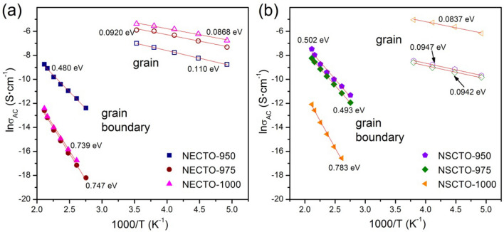
To optimize the results, the temperature dependence of AC conductivities (σAC) was measured in the temperature range of 103–473 K for NECTO and NSCTO ceramics, as illustrated in Fig. 10. Moreover, the activation energy required for the AC conductivities of charge carriers in the grains and grain boundaries can be calculated using the Arrhenius law41:
| 1 |
where σAC is the AC conductivity, σo is the pre-exponential term, Ea is the activation energy, and κB (J/K) and T are the Boltzmann constant and absolute temperature (K), respectively. According to Eq. (1), the values of activation energies (Eg for grain, Egb for grain boundary and Es for surface) can be calculated by fitting the curves in Fig. 10. Both Eg and Egb values of NECTO ceramics had different trends with the change of sintering temperature, as displayed in the Fig. 10a. The Eg of NECTO-950, NECTO-975 and NECTO-1000 ceramics were 0.110, 0.092 and 0.0868 eV, respectively. A slight decrease in Eg is consistent with the increase of grain conductivity shown in the Table 2. Meanwhile, with the increase of sintering temperature, the Egb values of NECTO ceramics were 0.480, 0.747 and 0.739 eV, respectively. As shown in the Fig. 10b, the observed Eg values of NSCTO-900, NSCTO-975 and NSCTO-1000 ceramics were 0.0947, 0.0942 and 0.0837 eV, respectively, while the observed Egb values were 0.502, 0.493 and 0.783 eV, respectively. The Eg values of NECTO and NSCTO ceramics were basically similar to the values of high-frequency relaxation activation energy obtained in Fig. 8, which further indicated that the dielectric response in the high frequency region was related to the grain. The changing trend of Eg and Egb values of NSCTO samples with sintering temperature was very similar to that of NECTO samples. Compared with NECTO-950, NSCTO-950 and NSCTO-975 ceramics sintered at low temperature, Egb and Eg values of the other ceramics prepared at high sintering temperature differed significantly, indicating that the IBLC polarization mechanism was formed, which will caused the giant dielectric response observed in NECTO-975, NECTO-1000 and NSCTO-1000 ceramics. The calculated Egb and Eg values were nearly same as other reported in CCTO and TiO2-related ceramics29,49–51.
Figure 10.
Arrhenius plots for the temperature dependence of σAC for (a) NECTO and (b) NSCTO samples. Red solid lines are the linear fitting curves.
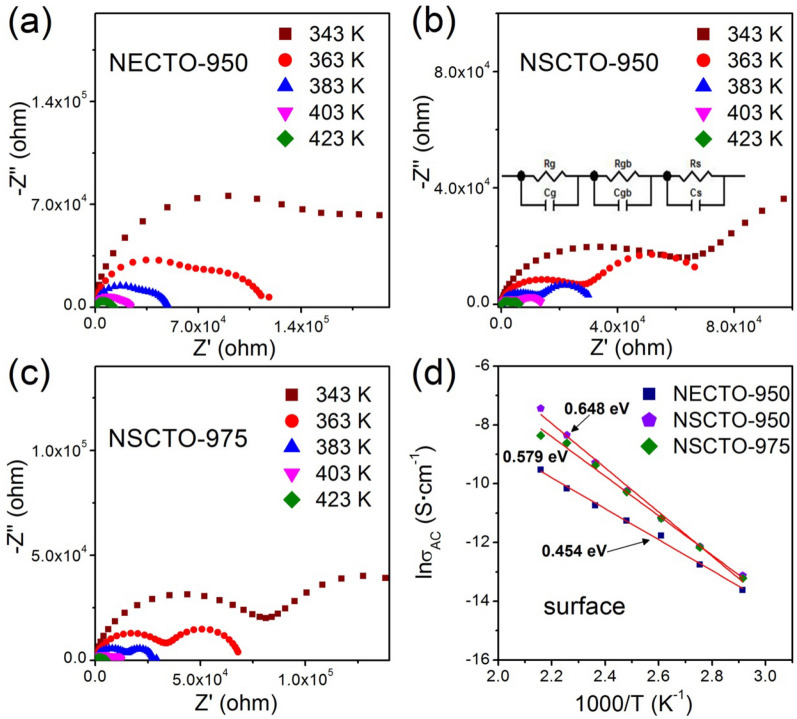
However, the abnormal high dielectric constant and dielectric loss observed in the low frequency for NECTO-950, NSCTO-950 and NSCTO-975 ceramics (shown in the Fig. 7) cannot be attributed to the IBLC effect. According to the analysis of Fig. 8, it could be governed by the polarization mechanism of SBLC. To confirm the possible source of the abnormal dielectric response in these ceramics, impedance complex spectrum of variable temperature (343–423 K) was displayed in the Fig. 11a–c, respectively. Because polycrystalline ceramic materials generally exhibit grain, grain boundary or surface impedances23, they can be represented by the equivalent circuit shown in Fig. 11b. Meanwhile, the Arrhenius plots of ac conductivity (σAC) for these three samples displayed in the Fig. 11d. It was observed that a new diameter of the semicircle arcs of the NECTO-950, NSCTO-950 and NSCTO-975 samples in the low frequency decreased with increasing temperature, which was a thermal activation process. As displayed in the Fig. 11d and Table 2, the activation energy of Na1/2Eu1/2Cu3Ti4O12 and Na1/2Sm1/2Cu3Ti4O12 ceramics sintered at 950 or 975 °C were 0.454, 0.648 and 0.579 eV, respectively. Considering the activation energy obtained in Fig. 11d, this thermal excitation process at low frequency region did not represent the electrical response of the grain or grain boundary, but was caused by the surface effect12,36,38. It was indicated that abnormal dielectric response for NECTO-950, NSCTO-950 and NSCTO-975 ceramics could be attributed to interfacial polarization based on SBLC effect. This was also consistent with the result obtained in Fig. 8. Interestingly, the doping of (Na+, Eu3+) or (Na+, Sm3+) in CCTO lattice could induce the appearance of Cu+ and Ti3+ in the grain during the sintering process. The low concentration of variable valence ions in the lattice could result in a small conductivity inside the grain at relatively low sintering temperature (950 °C). The abnormal permittivity and dielectric loss was contributed from the SBLC polarization mechanism for NECTO-950 and NSCTO-950 ceramics. NECTO and NSCTO ceramics prepared at high sintering temperature (1000 °C) would have more charge carriers with the increase of Cu+ and Ti4+ ions in ceramic structure, resulting in the formation of semiconductive region inside the grain. So, the giant dielectric constant and low dielectric loss for NECTO-1000 and NSCTO-1000 ceramics had been derived from an IBLC effect. According to the conclusion of XPS, the doping of (Na+, Eu3+) in CCTO-based ceramic was more likely to produce Cu+ ions than the doping of (Na+, Sm3+) in these ceramic. Therefore, the IBLC polarization mechanism appeared in the NECTO-975 ceramic containing high concentration of Cu+, and the ceramic showed good dielectric stability. On the contrary, SBLC polarization mechanism appeared in NSCTO-975 with abnormal dielectric response, while Cu+ ion was relatively low in the ceramic. In summary, the number of charge carriers (vacancies or free electrons) in the ceramic lattice will impress the conductivity of the grains, resulting in a competitive coexistence between SBLC and IBLC effects, thereby affecting the dielectric properties of ceramic.
Figure 11.
Impedance complex plane plots in the temperature range of 343–423 K for (a) NECTO-950, (b) NSCTO-950 and (c) NSCTO-975 ceramics; (d) Arrhenius plots of ac conductivity (σAC) for these three samples. Red solid lines are the linear fitting curves. Equivalent circuit indicated in frame (b) is used to represent the electrical properties of grain, grain boundary and surface effects.
Conclusion
This work systematically dealt with the structural, ion valence and dielectric properties of Na1/2Eu1/2Cu3Ti4O12 and Na1/2Sm1/2Cu3Ti4O12 ceramics sintered at different temperature. According to the XRD and RS data, all ceramics showed a single phase of CCTO-related ceramics. The substitutions of (Na+, Eu3+) or (Na+, Sm3+) in the CCTO lattice could induce the appearance of Cu+ and Ti3+ in grain. The higher sintering temperature, the more content of Cu+ and Ti3+, and the higher conductivity of grain in Na1/2Eu1/2Cu3Ti4O12 and Na1/2Sm1/2Cu3Ti4O12 ceramics, which also led to the gradual transformation of the polarization mechanism inside the ceramics from SBLC to IBLC. Therefore, Na1/2Eu1/2Cu3Ti4O12 and Na1/2Sm1/2Cu3Ti4O12 ceramics sintered at 1000 °C had giant dielectric permittivity of about 104, a low dielectric loss of about 10−2 and good frequency stability of about 102–106 Hz. At the same sintering temperature, the doping of Eu ions in the Na1/2Ln1/2Cu3Ti4O12 system would induce from more Cu+ ions inside the ceramics than the doping of Sm ions during the process of preparation. This resulted in a more pronounced IBLC polarization mechanism in Na1/2Eu1/2Cu3Ti4O12 ceramics than in Na1/2Sm1/2Cu3Ti4O12 ceramics. Therefore, Na1/2Eu1/2Cu3Ti4O12 ceramic prepared at 975 °C had better dielectric stability than Na1/2Sm1/2Cu3Ti4O12 ceramic sintered at same temperature.
Acknowledgements
This work was financially supported in part by Youth Science Foundation of Guizhou Province Education Ministry (QJHKY[2020]098), Scientific Research Foundation of Guizhou Province (QKHPTRC[2018]5784-02) and Doctor Foundation of Zunyi Normal collage (ZSBS[2019]03).
Author contributions
L.-F.Y. and D.-D.H. did the material prepared/characterizations and electrical measurements of the samples. L.-F.Y. and T.Z. clarified the experimental data and came out with the manuscript. L.-F.Y. is the group leader and conducted the investigation of this work. All authors reviewed the manuscript.
Data availability
All data generated or analysed during this study are included in this published article.
Competing interests
The authors declare no competing interests.
Footnotes
Publisher's note
Springer Nature remains neutral with regard to jurisdictional claims in published maps and institutional affiliations.
References
- 1.Wang L, et al. Study on the preparation and mechanical properties of purple ceramics. Sci. Rep. 2023;13:8755. doi: 10.1038/s41598-023-35957-0. [DOI] [PMC free article] [PubMed] [Google Scholar]
- 2.Cao Z, An S, Song X. Effect of thermal treatment at high temperature on phase stability and transformation of Yb2O3 and Y2O3 co-doped ZrO2 ceramics. Sci. Rep. 2022;12:9955. doi: 10.1038/s41598-022-13705-0. [DOI] [PMC free article] [PubMed] [Google Scholar]
- 3.Du C, et al. Fabrication of high radiation efficiency dielectric resonator antenna array using temperature stable 0.8Zn2SiO4–0.2TiO2 microwave dielectric ceramic. Adv. Mater. Technol. 2023;8:2201985. doi: 10.1002/admt.202201985. [DOI] [Google Scholar]
- 4.Chen Z, Zheng Y, Li B. A new microwave dielectric ceramic TmVO4 with high-quality factor and the effect of TiO2 on its microwave dielectric properties. J. Mater. Sci. Mater. Electron. 2023;34:828. doi: 10.1007/s10854-023-10254-8. [DOI] [Google Scholar]
- 5.Boonlakhorn J, Chanlek N, Suksangrat P, Thongbai P, Srepusharawoot P. Colossal dielectric properties of Na1/3Ca1/3Sm1/3Cu3Ti4O12 ceramics: Computational and experimental investigations. Ceram. Int. 2023;49:1690–1699. doi: 10.1016/j.ceramint.2022.09.131. [DOI] [Google Scholar]
- 6.Li Z, Wu J, Wu W. Composition dependence of colossal permittivity in (Sm0.5Ta0.5)xTi1−xO2 ceramics. J. Mater. Chem. C. 2015;3:9206–9216. doi: 10.1039/c5tc01659b. [DOI] [Google Scholar]
- 7.Tang H, Zhou Z, Sodano HA. Relationship between BaTiO3 nanowire aspect ratio and the dielectric permittivity of nanocomposites. ACS Appl. Mater. Interfaces. 2014;6:5450. doi: 10.1021/am405038r. [DOI] [PubMed] [Google Scholar]
- 8.Saengvong P, et al. Effects of sintering conditions on giant dielectric and nonlinear current–voltage properties of TiO2-excessive Na1/2Y1/2Cu3Ti4.1O12 ceramics. Molecules. 2022;27:5311. doi: 10.3390/molecules27165311. [DOI] [PMC free article] [PubMed] [Google Scholar]
- 9.Xu B, Zhang J, Tian Z, Yuan SL. Synthesis, dielectric and nonlinear electrical properties of Na1/2Bi1/2Cu3Ti4O12 ceramics by a sol–gel technique. Mater. Lett. 2012;75:87–90. doi: 10.1016/j.matlet.2012.01.025. [DOI] [Google Scholar]
- 10.Schmidt R, et al. Effects of sintering temperature on the internal barrier layer capacitor (IBLC) structure in CaCu3Ti4O12 (CCTO) ceramics. J. Eur. Ceram. Soc. 2012;32:3313–3323. doi: 10.1016/j.jeurceramsoc.2012.03.040. [DOI] [Google Scholar]
- 11.Subramanian MA, Li D, Duan N, Reisner BA, Sleight AW. High dielectric constant in ACu3Ti4O12 and ACu3Ti3FeO12 phases. J. Solid State Chem. 2000;151:323–325. doi: 10.1006/jssc.2000.8703. [DOI] [Google Scholar]
- 12.Variar L, Muralidharan MN, Narayanankutty SK, Ansari S. High dielectric constant and low-loss, carbon black/CaCu3Ti4O12/epoxy composites for embedded capacitor applications. Mater. Res. Bull. 2022;152:111835. doi: 10.1016/j.materresbull.2022.111835. [DOI] [Google Scholar]
- 13.Li J, Liang P, Yi J, Chao X, Yang Z. Phase formation and enhanced dielectric response of Y2/3Cu3Ti4O12 ceramics derived from the Sol–Gel process. J. Am. Ceram. Soc. 2015;98:795–803. doi: 10.1111/jace.13355. [DOI] [Google Scholar]
- 14.Kotb HM, Ahmad MM, Ansari SA, Kayed TS, Alshoaibi A. Dielectric properties of colossal-dielectric-constant Na1/2La1/2Cu3Ti4O12 ceramics prepared by spark plasma sintering. Molecules. 2022;27:779. doi: 10.3390/molecules27030779. [DOI] [PMC free article] [PubMed] [Google Scholar]
- 15.Gecil Evangeline T, Raja Annamalai A. Dielectric properties of conventional and microwave sintered Lanthanum doped CaCu3Ti4O12 ceramics for high-frequency applications. Ceram. Int. 2022;48:25705–25713. doi: 10.1016/j.ceramint.2022.05.179. [DOI] [Google Scholar]
- 16.Liang P, Yang Z, Chao X, Liu Z, Chen XM. Giant dielectric constant and good temperature stability in Y2/3Cu3Ti4O12 ceramics. J. Am. Ceram. Soc. 2012;95:2218–2225. doi: 10.1111/j.1551-2916.2012.05152.x. [DOI] [Google Scholar]
- 17.Boonlakhorn J, Manyam J, Krongsuk S, Thongbai P, Srepusharawoot P. Enhanced dielectric properties with a significantly reduced loss tangent in (Mg2+, Al3+) co-doped CaCu3Ti4O12 ceramics: DFT and experimental investigations. RSC Adv. 2021;11:25038–25046. doi: 10.1039/d1ra02896k. [DOI] [PMC free article] [PubMed] [Google Scholar]
- 18.Jumpatam J, et al. Effects of Mg2+ doping ions on giant dielectric properties and electrical responses of Na1/2Y1/2Cu3Ti4O12 ceramics. Ceram. Int. 2016;42:16287–16295. doi: 10.1016/j.ceramint.2016.07.167. [DOI] [Google Scholar]
- 19.Mahfoz Kotb H, Ahmad MM. Electrical and dielectric properties of Na1/2La1/2Cu3Ti4O12 ceramics prepared by high energy ball-milling and conventional sintering. Chin. Phys. B. 2016;25:128201. doi: 10.1088/1674-1056/25/12/128201. [DOI] [Google Scholar]
- 20.Jumpatam J, et al. Significantly improving the giant dielectric properties of CaCu3Ti4O12 ceramics by co-doping with Sr2+ and F- ions. Mater. Res. Bull. 2021;133:111043. doi: 10.1016/j.materresbull.2020.111043. [DOI] [Google Scholar]
- 21.Jumpatam J, Boonlakhorn J, Putasaeng B, Chanlek N, Thongbai P. Preparation, characterizations, dielectric properties and nonlinear behavior of (Na+1/3Ca2+1/3Yb3+1/3)Cu3Ti4O12 ceramics. Solid State Sci. 2022;132:106994. doi: 10.1016/j.solidstatesciences.2022.106994. [DOI] [Google Scholar]
- 22.Adams TB, Sinclair DC, West AR. Giant barrier layer capacitance effects in CaCu3Ti4O12 ceramics. Adv. Mater. 2002;14:1321–1323. doi: 10.1002/1521-4095(20020916)14:18<1321::AID-ADMA1321>3.0.CO;2-P. [DOI] [Google Scholar]
- 23.Sinclair DC, Adams TB, Morrison FD, West AR. CaCu3Ti4O12: One-step internal barrier layer capacitor. Appl. Phys. Lett. 2002;80:2153–2155. doi: 10.1063/1.1463211. [DOI] [Google Scholar]
- 24.Lindman A, Helgee EE, Wahnström G. Comparison of space-charge formation at grain boundaries in proton-conducting BaZrO3 and BaCeO3. Chem. Mater. 2017;29:7931–7941. doi: 10.1021/acs.chemmater.7b02829. [DOI] [Google Scholar]
- 25.Hu W, et al. Electron-pinned defect-dipoles for high-performance colossal permittivity materials. Nat. Mater. 2013;12:821. doi: 10.1038/nmat3691. [DOI] [PubMed] [Google Scholar]
- 26.Nachaithong T, Thongbai P, Maensiri S. Colossal permittivity in (In1/2Nb1/2)xTi1-xO2 ceramics prepared by a glycine nitrate process. J. Eur. Ceram. Soc. 2017;37:655–660. doi: 10.1016/j.jeurceramsoc.2016.09.006. [DOI] [Google Scholar]
- 27.Kum-onsa P, Thongbai P, Putasaeng B, Yamwong T, Maensiri S. Na1/3Ca1/3Bi1/3Cu3Ti4O12: A new giant dielectric perovskite ceramic in ACu3Ti4O12 compounds. J. Eur. Ceram. Soc. 2015;35:1441–1447. doi: 10.1016/j.jeurceramsoc.2014.11.028. [DOI] [Google Scholar]
- 28.Jumpatam J, et al. Non-ohmic properties and electrical responses of grains and grain boundaries of Na1/2Y1/2Cu3Ti4O12 ceramics. J. Am. Ceram. Soc. 2017;100:157–166. doi: 10.1111/jace.14473. [DOI] [Google Scholar]
- 29.Boonlakhorn J, Kidkhunthod P, Chanlek N, Thongbai P. (Al3+, Nb5+) co–doped CaCu3Ti4O12: An extended approach for acceptor–donor heteroatomic substitutions to achieve high–performance giant–dielectric permittivity. J. Eur. Ceram. Soc. 2018;38:137–143. doi: 10.1016/j.jeurceramsoc.2017.08.040. [DOI] [Google Scholar]
- 30.Qiu Y, et al. Grain size effect on the giant dielectric and nonlinear electrical behaviors of Bi1/2Na1/2Cu3Ti4O12 ceramics. Appl. Phys. A. 2012;107:379–383. doi: 10.1007/s00339-012-6806-9. [DOI] [Google Scholar]
- 31.Boonlakhorn J, et al. Dielectric properties with high dielectric permittivity and low loss tangent and nonlinear electrical response of sol-gel synthesized Na1/2Sm1/2Cu3Ti4O12 perovskite ceramic. J. Eur. Ceram. Soc. 2022;42:5659–5668. doi: 10.1016/j.jeurceramsoc.2022.06.030. [DOI] [Google Scholar]
- 32.Somphan W, Thongbai P, Yamwong T, Maensiri S. High Schottky barrier at grain boundaries observed in Na1/2Sm1/2Cu3Ti4O12 ceramics. Mater. Res. Bull. 2013;48:4087–4092. doi: 10.1016/j.materresbull.2013.06.028. [DOI] [Google Scholar]
- 33.Thongbai P, Yamwong T, Maensiri S. Dielectric properties and electrical response of grain boundary of Na1/2La1/2Cu3Ti4O12 ceramics. Mater. Res. Bull. 2012;47:432–437. doi: 10.1016/j.materresbull.2011.10.027. [DOI] [Google Scholar]
- 34.Kolev N, et al. Raman spectroscopy of CaCu3Ti4O12. Phys. Rev. B. 2002;66:132102. doi: 10.1103/PhysRevB.66.132102. [DOI] [Google Scholar]
- 35.Capsoni D, et al. Role of doping and CuO segregation in improving the giant permittivity of CaCu3Ti4O12. J. Solid State Chem. 2004;177:4494–4500. doi: 10.1016/j.jssc.2004.09.009. [DOI] [Google Scholar]
- 36.Lunkenheimer P, Fichtl R, Ebbinghaus SG, Loidl A. Nonintrinsic origin of the colossal dielectric constants in CaCu3Ti4O12. Phys. Rev. B. 2004;70:172102. doi: 10.1103/PhysRevB.70.172102. [DOI] [Google Scholar]
- 37.De la Rubia MA, et al. Dielectric behaviour of Hf-doped CaCu3Ti4O12 ceramics obtained by conventional synthesis and reactive sintering. J. Eur. Ceram. Soc. 2012;32:1691–1699. doi: 10.1016/j.jeurceramsoc.2012.01.024. [DOI] [Google Scholar]
- 38.Hu W, et al. Colossal dielectric permittivity in (Nb+Al) codoped rutile TiO2 ceramics: Compositional gradient and local structure. Chem. Mater. 2015;27:4934–4942. doi: 10.1021/acs.chemmater.5b01351. [DOI] [Google Scholar]
- 39.Biesinger MC, Lau LWM, Gerson AR, Smart RSC. Resolving surface chemical states in XPS analysis of first row transition metals, oxides and hydroxides: Sc, Ti, V, Cu and Zn. Appl. Surf. Sci. 2010;257:887–898. doi: 10.1016/j.apsusc.2010.07.086. [DOI] [Google Scholar]
- 40.Morita Y, et al. Valence fluctuations and correlated metallic states in A-site ordered perovskite oxides ACu3V4O12 (A=Na, Ca, and Y) Phys. Rev. B. 2010;81:165111. doi: 10.1103/PhysRevB.81.165111. [DOI] [Google Scholar]
- 41.Liu Z, Chao X, Liang P, Yang Z, Zhi L. Differentiated electric behaviors of La2/3Cu3Ti4O12 ceramics prepared by different methods. J. Am. Ceram. Soc. 2014;97:2154–2163. doi: 10.1111/jace.12940. [DOI] [Google Scholar]
- 42.Li M, et al. Origin(s) of the apparent high permittivity in CaCu3Ti4O12 ceramics: clarification on the contributions from internal barrier layer capacitor and sample-electrode contact effects. J. Appl. Phys. 2009;106:104106. doi: 10.1063/1.3253743. [DOI] [Google Scholar]
- 43.Thongbai P, Jumpatam J, Putasaeng B, Yamwong T, Maensiri S. The origin of giant dielectric relaxation and electrical responses of grains and grain boundaries of W-doped CaCu3Ti4O12 ceramics. J. Appl. Phys. 2012;112:114115. doi: 10.1063/1.4768468. [DOI] [Google Scholar]
- 44.Liu J, et al. Large dielectric constant and Maxwell–Wagner relaxation inBi2∕3Cu3Ti4O12. Phys. Rev. B. 2004;70:144106. doi: 10.1103/PhysRevB.70.144106. [DOI] [Google Scholar]
- 45.Ni L, Chen XM. Enhancement of giant dielectric response in CaCu3Ti4O12 ceramics by Zn substitution. J. Am. Ceram. Soc. 2010;93:184–189. doi: 10.1111/j.1551-2916.2009.03384.x. [DOI] [Google Scholar]
- 46.Somphan W, Sangwong N, Yamwong T, Thongbai P. Giant dielectric and electrical properties of sodium yttrium copper titanate: Na1/2Y1/2Cu3Ti4O12. J. Mater. Sci. Mater. Electron. 2011;23:1229–1234. doi: 10.1007/s10854-011-0578-4. [DOI] [Google Scholar]
- 47.Thongbai P, Jumpatam J, Yamwong T, Maensiri S. Effects of Ta5+ doping on microstructure evolution, dielectric properties and electrical response in CaCu3Ti4O12 ceramics. J. Eur. Ceram. Soc. 2012;32:2423–2430. doi: 10.1016/j.jeurceramsoc.2012.02.048. [DOI] [Google Scholar]
- 48.Yuan L, et al. CdO–CuO–TiO2 ternary dielectric systems: Subsolidus phase diagram and the effects of Cu segregation. J. Eur. Ceram. Soc. 2018;38:4978–4985. doi: 10.1016/j.jeurceramsoc.2018.07.038. [DOI] [Google Scholar]
- 49.Zheng P, Zhang JL, Shao SF, Tan YQ, Wang CL. Piezoelectric properties and stabilities of CuO-modified Ba(Ti, Zr)O3 ceramics. Appl. Phys. Lett. 2009;94:032902. doi: 10.1063/1.3072347. [DOI] [Google Scholar]
- 50.Bharti B, Kumar S, Lee H-N, Kumar R. Formation of oxygen vacancies and Ti3+ state in TiO2 thin film and enhanced optical properties by air plasma treatment. Sci. Rep. 2016;6:32355. doi: 10.1038/srep32355. [DOI] [PMC free article] [PubMed] [Google Scholar]
- 51.Wang C, et al. Relaxor-like behaviors in Na1/2Bi1/2Cu3Ti4O12 ceramics. J. Am. Ceram. Soc. 2017;100:2016–2023. doi: 10.1111/jace.14720. [DOI] [Google Scholar]
Associated Data
This section collects any data citations, data availability statements, or supplementary materials included in this article.
Data Availability Statement
All data generated or analysed during this study are included in this published article.


