Abstract
Thermomechanical analysis (TMA) is widely used to characterize materials and determine transition temperatures and thermal expansion coefficients. Atomic-force microscopy (AFM) microcantilevers have been used for TMA. We have developed a micromachined probe that includes two embedded sensors: one for measuring the mechanical movement of the probe (deflection) and another for providing localized heating. The new probe reduces costs and complexity and allow for portability thereby eliminating the need for an AFM. The sensitivity of the deflection element ((ΔR/R)/deflection) is 0.1 ppm/nm and its gauge factor is 3.24. The melting temperature of naphthalene is measured near 78.5 °C.
I. INTRODUCTION
Thermomechanical analysis (TMA) is widely used to characterize materials such as polymers and determine transition temperatures and thermal expansion coefficients. Typically a probe is placed on a sample with a known force. As temperature is increased, changes in the mechanical properties are recorded.1 Atomic-force microscopy (AFM) micro-cantilevers have been used for TMA to reduce analysis times, analyze small samples and provide spatial information.2–4 This is done by using a miniature heater probe with an AFM. The miniature cantilever probe is locally heated while the AFM photo-detector is used to monitor the deflection of the cantilever. Any changes such as transition temperatures can be identified from the probe movement.3,4
In this work we have developed a micromachined probe (piezo-thermal probe) that includes two embedded sensors: one for measuring deflection and another for providing localized heating. This probe reduces the cost and complexity associated with TMA by eliminating the need for an AFM or other TMA systems, while at the same time enhancing portability. Furthermore, this probe can be scaled to a probe array for high throughput melting point measurements.
Heating and deflection-sensing cantilevers have been independently developed in the past. These sensing elements are made by doping silicon5–7 or by depositing metal films on cantilevers.8 Cantilever metal sensing elements typically range in thickness from 100 nm to 30 nm.8 Metallic thin film sensing elements can have high temperature coefficients of resistance9 and high gauge factors.10 Thin film elements have other important advantages, including simplified fabrication and a lower manufacturing cost.9 Metallic sensing elements also enable the use of alternative substrate materials (such as polymers), that tend to exhibit higher compliance properties and improved thermal isolation.9
The probes described in this paper include a monolithic integration of a heating element (which can also be used for temperature sensing) and a deflection (or displacement) sensing element. Gold films of 10 nm thickness were deposited on a silicon cantilever to form both sensing elements. Integration of these functions within a single cantilever is expected to increase sensitivity, reduce the overall complexity of the setup and reduce cost.
II. DEVICE and FABRICATION
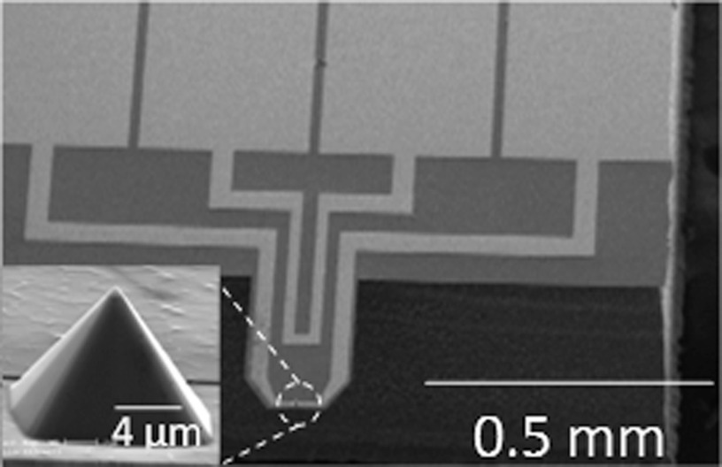
Figure 1 shows the piezo-thermal probe developed in this effort. This design includes two sensing elements on one cantilever, each of which consists of a 10 nm gold film located on a silicon cantilever. The resistor covering the tip area forms a microbolometer/microheater and the resistor near the base of the cantilever forms a deflection sensing element. The rectangular cantilever is 200 μm wide and 300 μm long. It is a stacked structure of silicon and silicon oxide layers with a total thickness of 2 μm. A (3 × 1.4 × 0.5) mm3 chip serves as the base of the cantilever.
FIG. 1.
SEM picture of fabricated piezo-thermal probe. Inset: Probe tip (<1 μm).
The device is fabricated with a four-mask process. The process starts with a silicon oxide insulator (SOI) wafer. A thermal oxide masking layer is deposited and patterned for the probe tip. The tip is formed using potassium hydroxide (KOH, 30 wt. %) anisotropic etching. The oxide masking layer is then removed and the tip is sharpened with several oxide sharpening steps.11 A silicon oxide layer 100 nm thick is thermally grown on the wafer to provide electrical insulation. The cantilever is patterned on the front side of the wafer. Metal lines are deposited on top of the cantilever structure to form the sensing and heating elements. The chip is then shaped by a back side deep reactive-ion etching (DRIE) process. The buried oxide layer of the SOI wafer acts as an etch stop to prevent the DRIE from attacking the silicon (Si) cantilever structures. The probes are finally released by removing the buried oxide layer using buffered hydrofluoric acid etchant.
III. SCANNING SYSTEM
For these measurements a scanning system is developed. The system includes a closed loop piezoelectric XYZ stage with 100 μm range on each axis and nanometer resolution (Tritor 100 PiezoJena) and an XYZ motorized stage with motion range of 28 mm on each axis and 0.05 μm microstep resolution (Zaber, model KT-LS28-MV). The system includes a holder for the piezo-thermal probe. A microscope is used to focus on the probe. The sample is brought in contact with the probe while monitoring the probe optically and electrically via the response of the deflection sensing element. All measurements were conducted in room temperature and atmospheric pressure.
The resistive change with distance of the deflection sensing element was directly measured using a micro-Ohm meter (Agilent, model 34420A), without the need of an interface amplifying circuit. The data are acquired with a LABVIEW program. A piezoelectric XYZ stage, described previously, is used to move the sample underneath the probe.
IV. EXPERIMENTAL RESULTS
A. Displacement sensing
After removing the parasitic resistance, the resistance of the displacement sensing element is approximately 105.4 Ω. Additional resistances from cabling and wirebonding are less than 1 Ω and, therefore, do not have a significant contribution to the overall resistance. The noise spectrum of the deflection sensing element is measured and found to be dominated by Johnson noise. 1/f noise is not observed.
The attractive and repulsive forces between a probe tip and sample surface are of interest as they can provide information about mechanical properties of the probe and of the sample (such as adhesion and elasticity). On AFMs, this can be done by analyzing the force vs. displacement (or distance) curves that can be routinely generated with the optical deflection measurement. Typically, the cantilever is moved vertically toward the sample (trace) and then away from the sample (re-trace). The deflection of the cantilever is plotted against the Z-axis scanner movement and then analyzed.
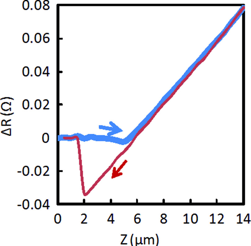
The change in resistance of the deflection sensing element with displacement (piezoresistance vs. distance curve) of the probe generated on glass is shown in Fig. 2. The curve is similar to a force-curve obtained with an AFM. However, in an AFM this measurement is limited by the piezoelectric tube scanner range, which is usually about 5 μm. In contrast the closed-loop piezoelectric XYZ stage we used allows us to monitor and measure interactions at a much larger range. The change in resistance can then be translated into the change in force as described in Ref. 12, which can then be used to extract the attractive and repulsive forces, as well as corresponding material properties.
FIG. 2.
The vertical axis is the change of the resistance of the deflection sensing element measured with a multimeter, whereas the horizontal axis is the Z-axis movement toward and away from the probe. The blue thick line represents the trace (i.e., the glass substrate moving toward the probe) and the red thin line represents the re-trace (i.e., glass substrate moving away from the probe).
At the value of 0 μm on the Z-axis the probe tip is not touching the sample. As the value on the Z-axis increases, the sample is brought closer to the tip. An attractive force deflects the probe toward the sample and, thus, there is a decrease in the resistance of the sensing element. A repulsive force deflects the probe away from the sample and there is an increase in resistance. When the probe gets very close to the sample (Fig. 2), it jumps into contact due to a sufficiently strong attractive force. As soon as the tip is in contact with the sample, the probe starts being pushed into the sample and the deflection will increase. This is translated into an increase in the slope of the curve in Fig. 2, which indicates that contact occurs around a value of 5 μm on the Z-axis. This value is arbitrary because the initial probe-sample distance is randomly chosen for this measurement. The slope and shape of the line is a measure of the elasticity of both the sample and the probe. The slope of the line on a hard glass is 0.01 Ω/μm (Fig. 2). Therefore, a 1 μm movement corresponds to ∼0.01 Ω change in the resistance. In addition, from Fig. 2 the deflection sensitivity of the probe ((ΔR/R)/deflection) is calculated to be 0.1 ppm/nm.
After reaching a certain predetermined Z-axis value the sample is moved away from the probe (re-trace). Initially, the curve is similar to the trace curve (approach). The adhesive forces cause the probe to stay adhered to the sample even after passing the initial contact point. After moving a further distance away from the sample the adhesion is broken, and this value corresponds to the rupture force, which is the force required to break the adhesion from the surface. For Fig. 2, this value represents a change in resistance of ΔR = 0.03 Ω.
The change in resistance, ΔR, can be converted into a corresponding force value using the gauge factor. The gauge factor of the deflection sensing element is given by the following equation:
| (1) |
where K is the gauge factor, E is the Young's modulus of the cantilever material, and σ is the average stress of the metal sensor. The average stress of the sensor can be estimated using cantilever analysis.13,14 The overall equation thus becomes
| (2) |
where λ is the length of the deflection sensing element from the base of the cantilever, L and t are the length and thickness of the cantilever, respectively, Δz is the displacement of the cantilever at the tip. Using Eq. (2) and the experimental data shown in Fig. 2, the gauge factor of the sensor is calculated to be 3.24.
B. Thermomechanical analysis
Precise temperature calibration is required for melting point measurements where temperature must be controlled with accuracy. A number of ways used to calibrate a thermal probe have been comprehensively reviewed15–17 and include: isothermal (hotplate) calibration,18 melting point standard calibration,19–21,24 using the linearity of heater resistance with temperature,25 and calibration methodology using Raman thermometry.16 Here we use a small thermocouple of the same size as the tip to calibrate the probe. The difficulty in determining the temperature at the interface of the probe-sample has been identified by others.17,22 Since the relation between power or resistance and temperature is dependent on substrate heat losses, all of the existing calibration methods will be somewhat affected by different samples. In order to estimate the temperature at the interface, thermal resistance circuits of the probe and sample have been developed.22,23 The main mechanism of heat transfer from the tip to the substrate is by conduction.15,22,26–28 In our case the tip is covered with a thin film of gold, which has a thermal conductivity of 318 W/mK. The thermal conductivity of naphthalene is 0.12 W/mK. The temperature of the tip, as derived from the thermal circuit, is very close to the temperature at the interface given that the thermal conductivity of naphthalene is very small compared to the thermal conductivity of gold. Thermal conduction (and contact resistance) at the interface depends on the contact area and the contact pressure.17,29 In this work we use the force vs. displacement curve to control the contact pressure. Based on our thermal calibration method, as described below, we have experimentally measured the melting point of naphthalene with 3.6% deviation from the standard value provided by the manufacturer.
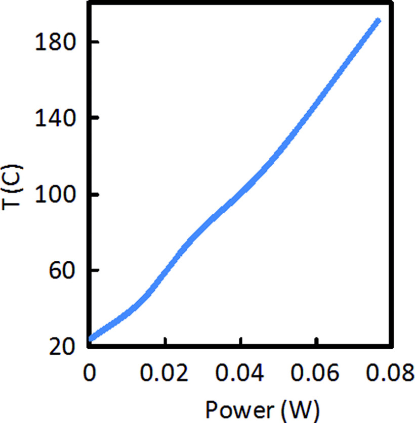
As discussed above, the heater is independently calibrated using a 12 μm size thermocouple (Omega, CHAL-0005) that is brought into contact with the heating element. The cantilever is placed on a motorized stage. A variable power supply (Keithley 2400) is used to increase the power through the heating element while monitoring the temperature with the thermocouple. Figure 3 shows the near linear relationship of the power through the heating element with temperature. Figure 3 is used to derive the temperature from a known value of power through the heating element.
FIG. 3.
A near linear relationship of power with temperature is observed. A variable power supply (Keithley 2400) was used to increase the power through the heating element while monitoring the temperature with an external thermocouple brought in contact with the tip.
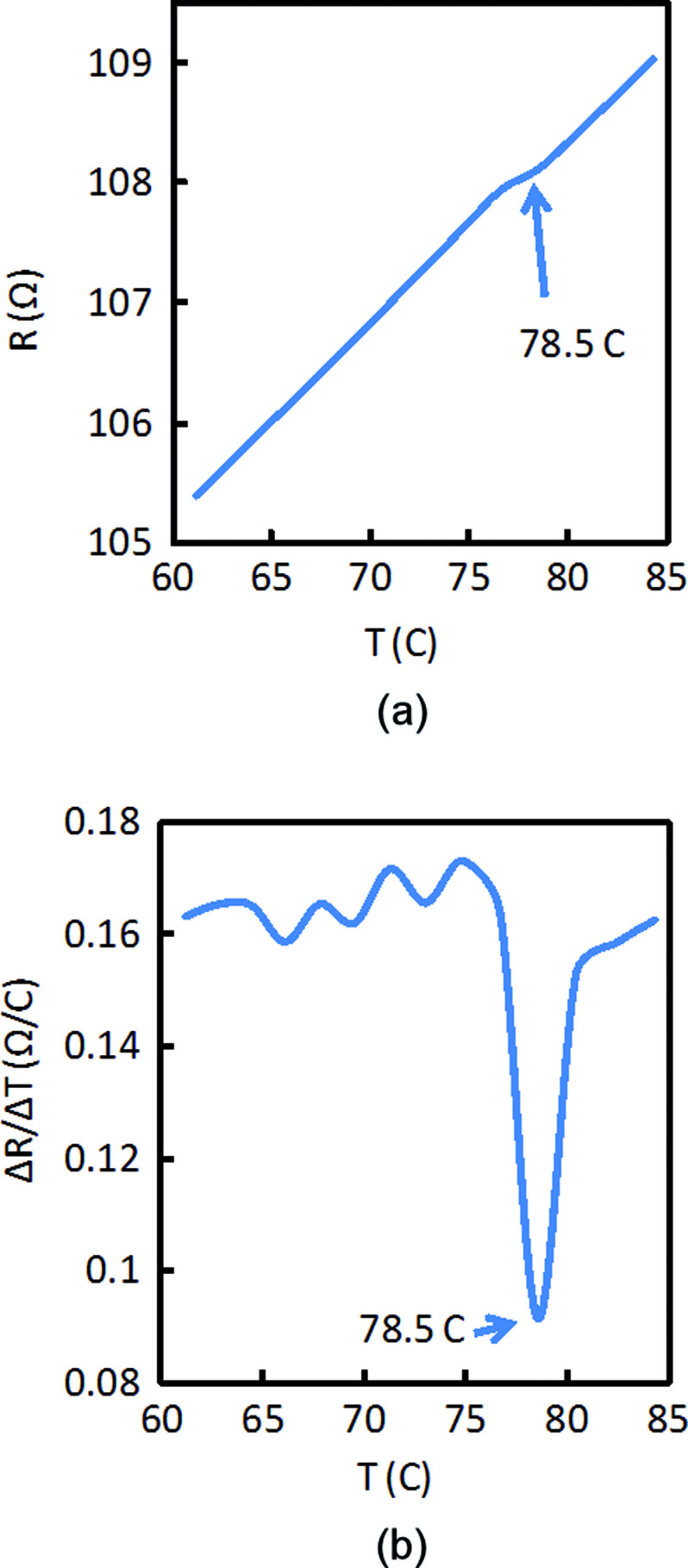
The melting temperature of naphthalene C10H8 (Sigma-Aldrich, Inc., 01422-250MG, Melting Point Standard) with a melting point between 79 °C —81 °C (±0.3 °C) is measured with the piezo-thermal probe. First, the sample and probe are brought in contact and a curve similar to Fig. 2 is produced to estimate the exact point of contact. A variable power supply is used to increase the power through the heating element in small increments (with heating rates up to 25 °C/sec), while the change in resistance of the deflection sensing element is directly measured using a micro-Ohm meter. The calibration curve of Fig. 3 is used to convert power to the corresponding temperature. Figures 4(a) and 4(b) show the change in resistance (Fig. 4(a)) and the change in the first order derivative (dRpiezo/dT) (Fig. 4(b)) of the deflection sensing element on the vertical axis with temperature increase of the heating element on the horizontal axis. As expected the increase in temperature caused by incremental increase in power through the heating element also increases the resistance of the nearby deflection sensing element. However, near the reported melting temperature a local decrease in resistance is observed in Fig. 4(a) at 78.5 °C. In Fig. 4(b), a local minimum is observed at 78.5 °C. The local decrease in resistance is interpreted as a movement of the probe toward the sample, an indent, caused from the melting.
FIG. 4.
The melting temperature of naphthalene was measured with the piezo-thermal probe. Figure 4(a) shows the change in resistance of the deflection sensing element on the vertical axis with temperature increase of the heating element on the horizontal axis. As expected the increase in temperature caused by incremental increase in power through the heating element also increases the resistance of the deflection sensing element. Figure 4(b) shows the first order derivative (dRpiezo/dT) of the deflection sensing element on the vertical axis with temperature increase of the heating element on the horizontal axis. Near the reported melting temperature a local decrease in resistance is observed in both Figs. 4(a) and 4(b) at 78.5 °C indicating a glass transition.
V. CONCLUSION
In conclusion, we developed a micromachined piezo-thermal probe that includes two monolithically integrated sensors: one for measuring the mechanical movement of the probe and another for providing localized heating, therefore, eliminating the need for an AFM. An ultrathin gold film with 10 nm thickness was deposited on a silicon cantilever to form both sensing and heating elements. The change in resistance of the deflection sensing element with displacement is used to estimate the point of contact. The sensitivity of the deflection sensing element ((ΔR/R)/deflection) is 0.1 ppm/nm and its gauge factor is 3.24. The melting temperature of naphthalene is measured (with heating rates up to 25 °C/sec) near 78.5 °C, which is close to the reported melting point (79–81 °C ±0.3 °C).
ACKNOWLEDGMENTS
We are grateful to Professor Yogesh Gianchandani, Professor Paddy French, and Dr. Cheryl Albus for their useful advice and help. This work was supported by the National Science Foundation (NSF) Award No. 0822810.
REFERENCES
- 1. Riga A. T., Materials Characterization by Thermomechanical Analysis (ASTM Special Technical Publication), edited by Neag C. M. (ASTM Intl., 1991). [Google Scholar]
- 2. Hammiche A., Pollock H. M., and Reading M., U.S. patent 6,200,022 (13 March, 2001).
- 3. Price D. M., Reading M., Hammiche A., and Pollock H. M., Int. J. Pharm. 192(1), 85 (1999). 10.1016/S0378-5173(99)00275-6 [DOI] [PubMed] [Google Scholar]
- 4. Hammiche A., Bozec L., Conroy M., Pollock H. M., Mills G., Weaver J. M. R., Price D. M., Reading M., Hourston D. J., and Song M., J. Vac. Sci. Technol. B 18, 1322 (2000). 10.1116/1.591381 [DOI] [Google Scholar]
- 5. Chui B. W., Mamin H. J., Terris B. D., Stowe T. D., Rugar D., and Kenny T. W., Appl. Phys. Lett. 69, 2767 (1996). 10.1063/1.117669 [DOI] [Google Scholar]
- 6. Chui B. W., Stowe T. D., Ju Y. S., Goodson K. E., Kenny T. W., Mamin H. J., Terris B. D., J. Microelectromech. Syst. 7(1), 69 (1998). 10.1109/84.661386 [DOI] [Google Scholar]
- 7. Tortonese M., Barrett R. C., and Quate C. F., Appl. Phys. Lett. 62, 834 (1993). 10.1063/1.108593 [DOI] [Google Scholar]
- 8. Li M., Tang H. X., and Roukes M. L., Nat. Nanotechnol. 2, 114 (2007). 10.1038/nnano.2006.208 [DOI] [PubMed] [Google Scholar]
- 9. Gaitas A., Zhu W., Gulari N., Covington E., and Kurdak C., Appl. Phys. Lett. 95, 153108 (2009). 10.1063/1.3250434 [DOI] [Google Scholar]
- 10. Li C., Hesketh P., and Maclay G., J. Vac. Sci. Technol. A 12, 813 (1994). 10.1116/1.578828 [DOI] [Google Scholar]
- 11. Akamine S., Barrett R. C., and Quate C., Appl. Phys. Lett. 57, 316 (1990). 10.1063/1.103677 [DOI] [Google Scholar]
- 12. Calleja M., Rasmussen P. A., Johansson A., and Boisen A., Proc. SPIE 5116, 314 (2003). 10.1117/12.498934 [DOI] [Google Scholar]
- 13. Thaysen Jacob, Ph.D. dissertation (Technical University of Denmark, 2001). [Google Scholar]
- 14. Sarid D., Scanning Force Microscopy: With Applications to Electric, Magnetic, and Atomic Forces I–XI, (Oxford University Press, New York, 1991), p. 253. [Google Scholar]
- 15. Nelson Brent A., “Nanoscale Thermal Processing Using A Heated Atomic Force Microscope Tip,” Ph.D. dissertation (Georgia Institute of Technology, 2007). [Google Scholar]
- 16. Nelson B. A. and King W. P., Sens. Actuators, A 140, 51 (2007). 10.1016/j.sna.2007.06.008 [DOI] [Google Scholar]
- 17. Fischer H., J. Therm Anal. Calorim. 92(2), 625 (2008). 10.1007/s10973-007-8554-1 [DOI] [Google Scholar]
- 18. Chui B. W., Stowe T. D., Ju Y. S., Goodson K. E., Kenny T. W., Mamin H. J., Terris B. D., Ried R. P., and Rugar D., J. Microelectromech. Syst. 7, 69 (1998). 10.1109/84.661386 [DOI] [Google Scholar]
- 19. Gianchandani J.-H. Lee and Y. B., Rev. Sci. Instrum. 75, 1222 (2004). 10.1063/1.1711153 [DOI] [Google Scholar]
- 20. Fryer D. S., Nealey P. F., and de Pablo J. J., Macromolecules 33, 6439 (2000). 10.1021/ma0003349 [DOI] [Google Scholar]
- 21. Blaine Roger L., Slough C. Gray, and Price Duncan M., in Proceedings of the Twenty-Seventh Conference of the North American Thermal Analysis Society, Savannah, GA, 20-22 September 1999, edited by Williams K. R. (North American Thermal Analysis Society, 1999). [Google Scholar]
- 22. Nelson B. A. and King W. P., Rev. Sci. Instrum. 78, 023702 (2007). 10.1063/1.2435589 [DOI] [PubMed] [Google Scholar]
- 23. Yue Zhaoyang and Liu Xianping, Key Eng. Mater. 437, 374 (2010). 10.4028/www.scientific.net/KEM.437.374 [DOI] [Google Scholar]
- 24. Hammiche A., Hourston D. J., Pollock H. M., Reading M., and Song M., J. Vac. Sci. Technol. B 14, 1486 (1996). 10.1116/1.589124 [DOI] [Google Scholar]
- 25. Lee J. and Gianchandani Y. B., J. Microelectromech. Syst. 14, 44 (2005). 10.1109/JMEMS.2004.839011 [DOI] [Google Scholar]
- 26. King W. P. and Goodson K. E., “Thermomechanical formation and thermal imaging of polymer nanostructures,” in Heat Transfer and Fluid Flow in Microscale and Nanoscale Devices, edited by Faghri M. and Sunden B., (WIT Press, Southampton, UK, 2002), pp. 131–171 [Google Scholar]
- 27. Li Mo-Huang, “Surface Micromachined Polyimide Scanning Thermocouple and Bolometer Probes,” Ph.D. dissertation (University of Wisconsin-Madison, 2001). [Google Scholar]
- 28. Lefèvrea Stéphane, Volzb Sebastian, and Chapuis Pierre-Olivier, Int. J. Heat Mass Trans. 49(1–2), 251 (2006). 10.1016/j.ijheatmasstransfer.2005.07.010 [DOI] [Google Scholar]
- 29. Nikiforov M. P. and Proksch Roger, “Dynamic SPM methods for local analysis of thermo-mechanical properties,” in Scanning Probe Microscopy of Functional Materials, Part 3, pp. 199–229.


