Abstract
The current demand for high-channel-count neural-recording interfaces calls for more area- and power-efficient readout architectures that do not compromise other electrical performances. In this paper, we present a miniature 128-channel neural recording integrated circuit (NRIC) for the simultaneous acquisition of local field potentials (LFPs) and action potentials (APs), which can achieve a very good compromise between area, power, noise, input range and electrode DC offset cancellation. An AC-coupled 1st-order digitally-intensive architecture is proposed to achieve this compromise and to leverage the advantages of a highly-scaled technology node. A prototype NRIC, including 128 channels, a newly-proposed area-efficient bulk-regulated voltage reference, biasing circuits and a digital control, has been fabricated in 22-nm FDSOI CMOS and fully characterized. Our proposed architecture achieves a total area per channel of 0.005 mm2, a total power per channel of 12.57 , and an input-referred noise of 7.7 ± 0.4 in the AP band and 11.9 ± 1.1 in the LFP band. A very good channel-to-channel uniformity is demonstrated by our measurements. The chip has been validated in vivo, demonstrating its capability to successfully record full-band neural signals.
Keywords: Neural recording, high-density, electrophysiology, analog-to-digital converter, brain-machine interface, continuous-time delta-sigma conversion
I. INTRODUCTION
FULLY-integrated and high-density neural recording probes are becoming vital neuroscience tools to perform massive recording of single-cell neural activity across different brain regions [1]-[5]. Thanks to the progress in neural recording devices, an exponential Moore’s-Law-like growth in recording density has been observed in the last decades [6]. However, this growth is still insufficient to enable large brain coverage with implantable probes. To further scale the capabilities of existing CMOS neural probes, several design challenges need to be tackled. First, higher channel area and power efficiencies need to be achieved to enable higher-density recording. For this, system-level co-optimization is crucial to obtain the best trade-off with other important specifications such as input range and noise. Since the frequency bandwidth of the neural local filed potentials (LFPs, 0.5-1000 Hz) lies in the flicker noise band and the bandwidth of the neural action potentials (APs, 0.3-10 kHz) is affected by thermal noise, the power-area-noise trade-off is not easy to address. The second challenge comes from the electrode DC offset (EDO) present at the electrode-tissue interface. This offset can be as large as tens or even hundreds of mV, and it can vary over time due to the electrochemical changes and reactions happening during a chronic implant. Since this offset is much larger than the neural-signal amplitudes (APs: 10’s of to ~1 mV; LFPs: 100’s of to ~5 mV [7]), it can easily saturate the readout circuits. Finally, the recording electrodes may also be subject to artifacts caused by body movement or concurrent electrical stimulation. The amplitudes of such artifacts are very difficult to quantify because they depend on many factors such as the electrode size, impedance and location, the type of motion the animal is doing, the location of the reference electrode, the distance between the recording and stimulation electrodes, and the amplitude of the stimulation current. Thus, the input range of the readout channel should be large enough to accommodate the LFP signals plus a certain amount of motion/stimulation artifacts without saturation. The input range will then determine the type of experiments that can be supported by the readout system (e.g. freely-moving animal or concurrent micro/macro stimulation experiments).
To tackle the forementioned challenges, diverse circuit techniques have been proposed. The most common neural readout architecture consists of multiple amplification channels which are multiplexed into one analog-to-digital converter (ADC) [3], [5], [8]-[23]. The amplification stage is typically implemented as an AC-coupled instrumentation amplifier (IA) which can easily reject the EDO. The electrical performance and robustness of such architecture have been extensively validated in large-scale and long-term recordings [24], [25], but it has not achieved yet a good trade-off between the different performance metrics. For instance, a very power- and area-efficient AC-coupled readout channel has been recently reported in [13], but its input range is too limited to tolerate possible movement/stimulation artifacts. In order to reduce the channel area, a multiplexed AC-coupled readout has been proposed in [26]. By multiplexing at the input of the channel, the equivalent area and power per electrode get significantly reduced by the multiplexing ratio. However, due to the lack of anti-aliasing filters before the multiplexer, the biological and electrode noise gets folded into the Nyquist band, thus increasing its contribution proportionally to the square root of the multiplexing ratio [4], [27]. Although this noise will dominate the total noise of the recording system, especially when using small and large-impedance electrodes, this contribution has not been properly included in the noise reported in [26]. Additionally, directly multiplexing at the electrode results in switching currents injected to/from the tissue, potentially posing safety issues in large-scale neural recording.
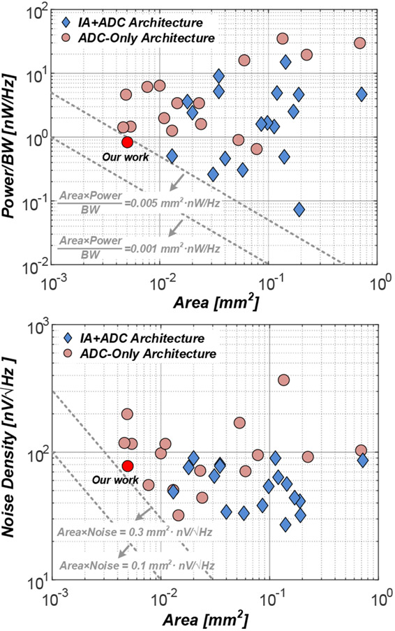
Direct-digitization topologies have been proposed as good alternatives to dramatically reduce the readout area and provide scalability in advanced technology nodes [2], [19], [28]-[44]. These architectures normally use or -like modulators since they can achieve good noise performance by combing oversampling and noise-shaping techniques. The low-noise front-end stage is then embedded in the mixed-signal loop of the modulator. Impressive area reductions have been achieved in some of these designs [2], [30], [37]. In [30], a 2nd-order DC-coupled ADC achieves a large dynamic range, small area and low noise, while the EDO is tolerated by the large input range of the ADC. However, the required high-order modulation loop and complex decimation filter lead to high power consumption. This limitation has been tackled in [37] by introducing an EDO compensation loop. In this way, a simplified first-order modulation loop could be implemented. However, the noise contribution from the extra compensation loop is not negligible, resulting in high noise in the presence of large EDOs. Fig. 1 compares the channel power and noise performances versus area for recently reported neural readout chips. The IA+ADC architectures can be made more power and noise efficient, but the smallest areas are achieved with direct-digitization architectures.
Fig. 1.
Performance comparison of state-of-art neural recording integrated circuits: IA+ADC architectures vs. ADC-only architectures. Data obtained from [1]-[3], [5], [8]-[23], [28]-[45]. Architectures with input multiplexers are not considered here since their noise performance is dominated by the aliased electrode/tissue noise.
In this paper, we propose an AC-coupled 1st-order neural recording integrated circuit (NRIC). By implementing a novel combination of system and block-level topologies, we achieve a good compromise between power, area, noise, input range and EDO tolerance. In this design, a integrator together with a current digital-to-analog converter (IDAC) are used to offer high-input impedance and enable AC-coupling for rail-to-rail EDO rejection. Delta-modulation around a core is used to extend the input range. The -modulation loop is implemented in the digital domain, thus requiring no extra IDAC and benefitting from scaled technologies. To validate the proposed architecture and demonstrate its performance and scalability, a 128-channel prototype chip has been fabricated in a 22-nm FDSOI CMOS technology. The prototype chip has been used to develop a small and lightweight headstage (HS) that can enable saline and in vivo measurements with passive neural probes. This paper is an extension of our previous report [45]. The rest of the paper is organized as follows. The complete system-level design and the working principle of the proposed architecture is presented in Section II. Section III covers the detailed circuit implementation of the main building blocks. The measurement results are summarized in Section IV and conclusions are drawn in Section V.
II. System Design
A. High-level NRIC Architecture
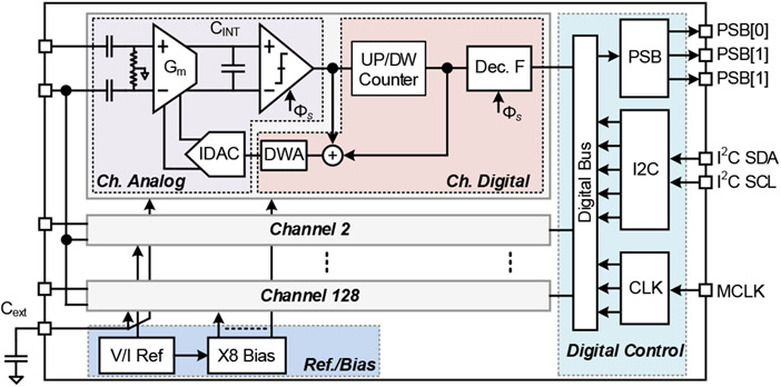
The complete system architecture of the NRIC is shown in Fig. 2. It consists of 128 recording channels, a reference and bias generator, and a digital control. The latter includes a digital serializer, an I2C interface, and a clock and control-signal generator to operate the channels. The NRIC operates with a supply voltage of 0.8 V and is clocked by a master clock of 48 MHz from which the internal clocks are derived.
Fig.2.
System architecture of the prototype NRIC
Each recording channel is based on a hybrid discrete-time continuous-time (DT-CT) modulator. Here, a based 1st-order core is embedded into a -modulation loop to provide multi-bit feedback from a one-bit quantizer. An up-down counter is used to form a digital integrator in the feedback loop and to achieve the -modulation. The quantizer consists of only a comparator, thus eliminating the need for a power-hungry reference buffer. Finally, data weighted averaging (DWA) provides 1st-order mismatch shaping for the elements in the IDAC. Compared with a single-bit modulator (e.g. [2]), the proposed topology increases the dynamic range and reduces the quantization error [30],[21]. Furthermore, the multi-bit feedback IDAC reduces the sensitivity to clock jitter which negatively affects CT modulators [46]. The input range of the modulator is determined by the total feedback current and the transconductance.
An AC-coupled stage is placed in front of the modulator to provide rail-to-rail EDO cancellation in a power- and area-efficient way. This enables the connection of the readout channel to any type of electrode, thus decoupling the circuit design constraints from the electrode performance. AC-coupling further reduces the area and power consumption of the whole modulator since only AC signals are digitized. The feedback integrator used for -modulation, as well as the summation with the feedback, are implemented in the digital domain to fully benefit from the scaled technology. First-order noise-shaping is used to minimize the power and area of the digital decimation filter and eliminate the need for additional integrators. All the above characteristics enabled a significantly lower power and smaller area compared with our previous DC-coupled 2nd-order design in [30], which has other important architectural differences such as the analog-domain delta-modulated feedback and the power-hungry 3rd-order decimation filter.
B. Proposed Hybrid CT-DT Front-End
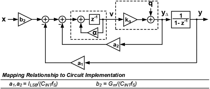
Figure 3 shows the DT-equivalent model of the proposed modulator. The feedback path employs a non-delaying integrator, thus corresponding to a cascade-of-resonators-feedback (CRFB) structure with zero coefficients for positive feedback [47]. Here, the DT equivalent of the CT integrator, formed by the operational transconductance amplifier (OTA) and , is determined considering the following correspondence valid over a full clock-cycle:
| (1) |
where , , , and . The parameter accounts for the leaky integration with time constant , where is the output impedance of the OTA. Note that when this pole is at a much lower frequency compared with the sampling rate , , hence .
Fig. 3.
DT equivalent model of the proposed 1st-order hybrid DT-CT modulator and its mapping relationship with the circuit implementation.
The signal transfer function (STF) and noise transfer function (NTF) of the modulator can be derived from (1) and are given by:
| (2) |
| (3) |
Where is the quantizer gain and:
| (4) |
The input-referred quantization error can be determined using (3). In fact, the single-sided power spectral density (PSD) of the quantization error at the quantizer output is:
| (5) |
where is the quantization step of the single-bit quantizer. Therefore, when referred to the input of the modulator, the quantization error is shaped according to:
| (6) |
Because of the high oversampling ratio (OSR = 160) chosen in this design, in the signal band, hence and:
| (7) |
The in-band noise power is then:
| (8) |
where . Note that is the least-significant bit (LSB) of the quantizer as referred to its input. When is very large (), we can approximate . Thus, the noise shaping degradation due to the leaky integration amounts to the fraction:
| (9) |
which can be maintained negligible if the corner frequency of the integrator is significantly smaller than . To ease the design of the stage, this constraint can be relaxed at the expense of noise degradation. In our case, we designed for MΩ while is 107 .
A high-level Simulink model of the channel modulator is employed to assess the maximum stable amplitude (MSA) and the stability of the modulator, estimating the quantizer gain from simulations [47]:
| (10) |
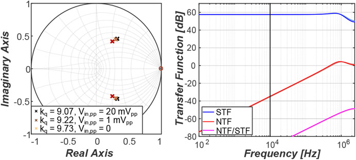
where are the samples of quantizer input. Three different values of are used to determine the pole-zero map and the STF and NTF (for an ideal integrator) as shown in Fig. 4. These values correspond to 3 different input amplitudes (0 V, 1 mVpp and 20 mVpp), indicating that must be considered to ensure stability over different conditions.
Fig. 4.
Pole-zero map with different quantizer gains under different input amplitudes and the corresponding signal and noise transfer functions.
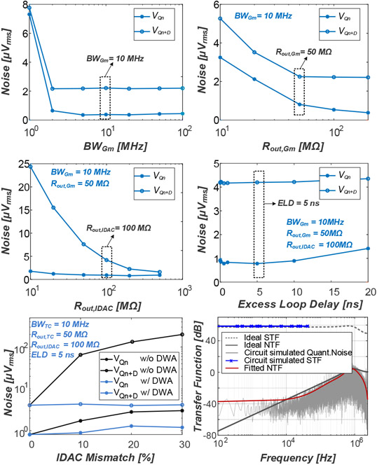
Other non-idealities such as the bandwidth of the OTA (), the output impedances of the OTA () and IDAC (), the excessive loop delay (ELD), and the IDAC mismatch were included in a Verilog-AMS model to determine the requirements of the main analog sub-blocks of the channel (OTA, IDAC and comparator). Fig. 5 shows the high-level simulation results where the input-referred noise () and the input-referred noise plus distortion () are used to determine the design specifications. The effectiveness of the DWA was also assessed in these simulations. Based on the simulation results, the final specifications are set as: MHz, MΩ, MΩ, ELD < 5 ns and IDAC mismatch < 30%, for which we can achieve a and a . For the ELD, a value of 5 ns, corresponding to 2.48% of a clock cycle, was found to not affect stability, as verified through both Verilog-AMS and transistor-level simulations.
Fig. 5.
System-level simulations of the input-referred quantization noise () and distortion () across different OTA bandwidths, OTA output impedances, IDAC output impedances, excess loop delays and IDAC mismatches with and without DWA, where the black-dashed rectangles show the selected design specifications. Bottom-right: circuit-level simulations of the NTF/STF with the final circuit specification.
To validate our Verilog-AMS model, we have performed circuit-level STF/NTF simulations using the final circuit specifications (Fig. 5 bottom-right). The STF is obtained by sweeping the input frequency and calculating the output magnitude of the modulator. The spectrum of the quantization noise floor is simulated, and the NTF is fitted in Matlab. As shown, the high-frequency part is close to the ideal NTF, while the lower frequency part is flat due to the non-idealities analyzed in Fig. 5. The detailed circuit implementation will be discussed in the following section.
III. Circuit Implementation
A. AC-Coupled Transconductance Stage
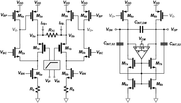
Figure 6 shows the schematic of the AC-coupled input stage. The input EDO gets filtered by the differential high-pass filter (HPF) formed by a pair of 5-pF MOM capacitors connected to thick-oxide PMOS pseudo-resistors. The cutoff frequency of the HPF is set to 0.1 Hz to enable the recording of both neural LFPs and APs, while limiting the noise contribution of the pseudo-resistor and the settling time of the channel. The area contribution of this HPF is negligible since the MOM capacitors are placed on top of the active circuits in the layout (i.e. no area overhead), and the pseudo-resistors are sized very small (). Since the voltage across the pseudo-resistors is only the small input signal, only limited linearity degradation is expected.
Fig. 6.
Schematic of the AC-coupled OTA stage.
The stage is implemented with a resistively-degenerated OTA. A pair of flipped voltage followers [48] (M1a,b-M4a,b) drives the polysilicon resistor . The low-impedance terminals and allow the feedback currents from the IDAC ( and ) to be subtracted from the current (). The resulting current is conveyed to the integrating capacitor, via unity-gain current mirrors (M3a,b and M6a,b). Degeneration resistors are employed to further minimize the noise from the bias transistors M5a,b. The input transistors M1a,b are implemented with thick-oxide devices to minimize the gate leakage flowing through the pseudo-resistors, which may affect the input DC bias of the stage, increase the HPF cut-off frequency and degrade the noise performance. Since the thick-oxide transistors in this scaled technology still exhibit a small amount of gate leakage, the size of M1a,b is chosen as a trade-off between area, noise, and high-pass corner frequency. To control the output common-mode (CM) voltage, a differential-difference-amplifier (DDA) based CM feedback (CMFB) circuit is utilized. It senses the output differential voltage and compares it with a reference voltage before feeding it back to the gate terminals of the NMOS transistors . Additionally, at frequencies beyond the bandwidth of the CMFB loop, there are CM ripples induced by the oversampling clock of the modulator. Hence, the integrating capacitor is split into two CM capacitors () and one differential-mode (DM) capacitor () where the mid-node of the CM capacitors provides high-frequency CMFB. This configuration helps reduce the clock-induced CM ripples. Our circuit-level simulations show that the stage achieves a bandwidth of 10.35 MHz and an output impedance of 59.5 MΩ.
B. Current-Steering DAC
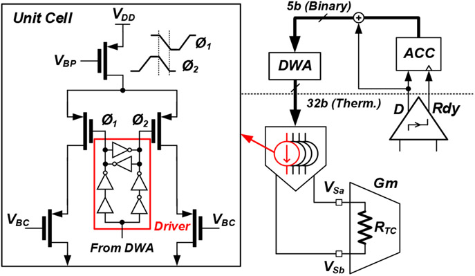
The IDAC in the feedback path includes 32 thermometric elements, each featuring a 2-level DAC. The circuit schematics of the IDAC and its unit element are shown in Fig. 7. Each unit cell is implemented by a small PMOS current source biased by . Thus, the entire 32-unit IDAC suffers from mismatch. This mismatch, together with the current glitches generated by the driving clock (Φ1,2), contribute to the overall modulator distortion. To limit this contribution, a latch driver (red box) is inserted to perfectly align the clocks, thereby reducing the current glitches. Additionally, DWA is applied to minimize the effect of the current-source mismatch. The simulated IDAC output impedance is 404 MΦ, with a unit mismatch factor of 6.3%.
Fig. 7.
Schematic of the current-steering DAC.
C. Comparator
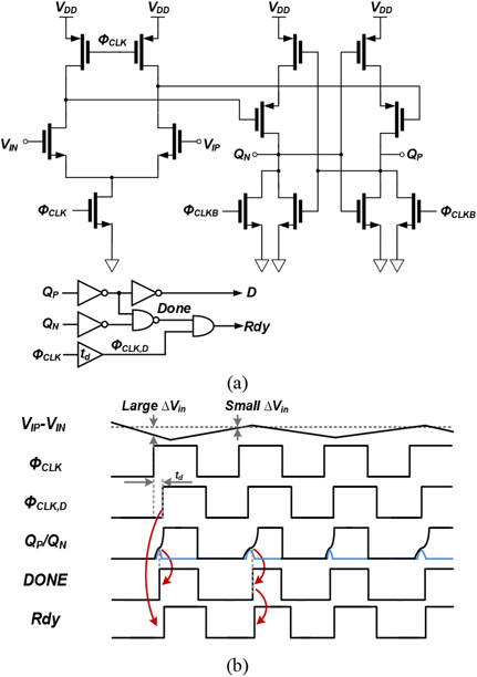
The dynamic comparator (Fig. 8(a)) employs an Elzakker's topology [49] to reduce the kickback noise. The use of a non-delaying integrator requires tighter timing (shorter delay) for the comparator decision and for the following digital block in the feedback loop. Therefore, the delay of the comparator, from the input clock ΦCLK to the output D, needs to be controlled to minimize the ELD and avoid generating a wrong digital code for the IDAC.
Fig. 8.
(a) Schematic of the 1-bit quantizer (comparator). (b) Timing diagram of the quantizer.
The comparator delay varies with the input signal, with longer delays expected for smaller input signals (up to metastability). Since the input of the comparator in this architecture is pseudorandom (i.e., quantization noise), the delay of the comparator is also pseudo-random. This phenomenon can degrade the noise-shaping akin to clock jitter [50]. To minimize this effect, the output of the comparator, which triggers the acquisition in the digital feedback via Rdy, is delayed by a fixed amount of time td. A longer decision time is allowed through the Done signal (which indicates that the latch outputs QP and QN have settled to logic levels) to resolve sporadic input signals with very small amplitude. A timing diagram of the relevant signals is shown in Fig. 8(b). This scheme causes some residual delay variations, but the occurrences of these events are only a small percentage of all comparisons as confirmed by our Monte-Carlo simulations. Thus, the in-band quantization error does not get significantly degraded. Since the ELD is increased temporarily only during very few and sparse clock cycles, the average values of the modulator coefficients (and hence the loop-gain) are only slightly modified [51]. Therefore, the stability of the modulator is not compromised.
D. Digital Feedback and Decimation Filter
An up-down counter integrates the captured bitstream from the comparator output D into a 5-bit signed signal at each clock cycle (with the clock given by the Rdy signal). The Rdy signal becomes active-high shortly after the rising edge of ΦCLK to indicate that the comparator decision is settled. With this behavior, the up-down counter is implemented as a non-delaying integrator. The adder sums the captured D and the output of the counter with minimum delay once the counter’s output is settled. The final output is fed into the DWA to provide the mismatch shaping characteristic to the IDAC. The digital backend synthesis indicates a worst-case ELD of 2.9 ns in the digital feedback, which is sufficiently low for our design.
A 2-stage cascaded integrator-comb (CIC) decimation filter is inserted at the counter’s output to suppress the out-of-band quantization noise and provide anti-aliasing filtering of the out-of-band signals and noise (e.g. circuit noise, electrode noise and background biological activity). This filter is configured with an input bit-width of 5 bits and an output bit-width of 14 bits, for an output sampling rate of 30 kS/s. Compared to the typical 1st-order analog low-pass filter employed in conventional channel architectures, this digital filter does not require bulky passives, is not susceptible to process-voltage-temperature variations and provides a steeper filtering characteristic.
F. Reference Generator
To reduce the complexity of the external acquisition system interfacing with our NRIC, the voltage and current references required to operate all the channels are integrated on chip. Therefore, the reference generator is also a critical block that contributes to the total area and power consumption. A bandgap reference (BGR) is a widely used architecture to generate a temperature insensitive reference voltage. It can achieve a good line sensitivity, but it is usually bulky and power hungry [52]. A much more compact voltage reference can be designed with the two-transistor (2T) structure proposed in [53]. It achieves a very small area and low power, but the line sensitivity of the output reference voltage is rather poor.
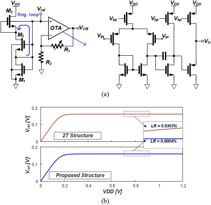
In this work, we propose a compact bulk-regulated voltage-reference circuit to overcome the abovementioned challenges (see Fig. 9 (a)). Transistors form the reference generator, while the output reference voltage () is further scaled to generate the 0.4-V CM voltage () for all channels. Two trimming bits are implemented to tune the resistance , enabling the compensation of possible process variations. The CM voltage is then used to generate eight reference currents for the eight channel groups present in the design. In order to facilitate the layout and optimize the drivability of the common bias voltages distributed to the stages and IDACs, each channel group consists of 16 channels and includes an independent biasing generator.
Fig. 9.
(a) Schematic of the proposed bulk-regulated reference generator. (b) Simulation results of the conventional 2T-structure and the proposed bulk-regulated reference generator where .
The working principle of the reference generator is the leakage-current-based 2T architecture formed by the stacked transistors and . Similar to [53], the reference voltage can be derived as:
| (11) |
where is the thermal voltage, is the threshold voltage, is the electron mobility, is the subthreshold slope factor, and and are the width and length of the two transistors. Eq. (11) can be divided into a complementary-to-absolute-temperature (CTAT) term and a proportional-to-absolute-temperature (PTAT) term. By properly sizing the parameters, can be made temperature insensitive. In our design, is a thick-oxide NMOS transistor, while is a flipped-well NMOS device (i.e. NMOS transistor in N-well).
The transistor is used here to regulate the drain-source voltage of . This is done by connecting to the bulk of , which is also a flipped-well device. In this way, the perturbations from the supply voltage to the drain of are reduced, and the line regulation of the output voltage improved [54]. Fig. 9 (b) shows the simulation comparison of the conventional 2-T reference generator and the proposed reference generator. The line regulation is improved from 0.0303% to 0.0004%.
The proposed 3-transistor (3T) reference generator consumes less than 0.1 nW at body temperature (37°C) and operates in deep weak inversion (aka ‘super cut-off’) region. The supply current flowing through all transistors is defined by , which has negative bulk-source and zero gate-source potentials. In this bias condition, only a few tens of pA can flow through the transistors, which is negligible compared to the power consumption of a conventional BGR.
IV. Measurement Results
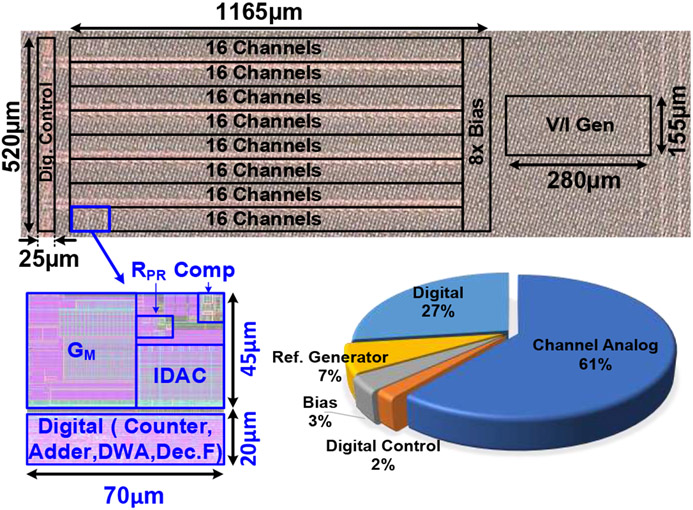
A prototype 128-channel NRIC was fabricated in a GlobalFoundries 22-nm FDSOI technology. It occupies a total active area of 0.66 mm2, including the 128 readout channels, the reference generator, the biasing circuits, and the digital control. Fig. 10. shows the chip micrograph and the area breakdown per channel. The channel area is only 70 × 65 , which includes both the analog and digital (integrator, adder, DWA and decimation filter) parts of the channel. As shown in the breakdown, 61% of the total channel area is occupied by the analog part of the modulator, which includes the integrator, the comparator, the IDAC and the AC-coupled input stage. Deep-NWELL isolation is used to shield the sensitive analog part of the channel from the substrate noise injected by the digital circuits. The total chip area per channel is 0.0051 mm2 when also considering the biasing circuits, the V/I reference generator and the digital control.
Fig. 10.
Micrograph of the fabricated 128-channel NRIC and the total channel area breakdown.
A. Electrical Characterization
To characterize the electrical performance of our NRIC, the dies were packaged on custom daughter printed-circuit boards and connected to a motherboard containing the required local components and connectors to operate the chip. The measurement setup is illustrated in Fig. 11. The boards are battery-powered, and a Stanford Research DS360 function generator is used to generate input sinusoidal signals. A Stanford Research SR560 low-noise amplifier is used to further filter-out the noise and mains interference of the sinusoidal signals, which are then applied to all the channel inputs. Finally, a National Instruments PXI-6544 acquisition card communicates with the chip through the I2C interface and collects the serial output data. A master clock of 48 MHz, provided by an external crystal oscillator, is used to generate on chip the 4.8-MHz oversampling clock and the 30-kHz down-sampling clock.
Fig. 11.
Measurement setup for chip electrical characterization.
With a supply voltage of 0.8 V, the measured total power consumption of the chip is 1.61 mW when all the 128 channels are active. This includes the power consumption of the GPIOs (541.4 ) during serial-data transmission. Therefore, the total power per channel is 12.57 , of which 3.29 (26%) are consumed by the channel analog circuit, 4.73 (38%) are consumed by the digital blocks and 4.23 (34%) are from the GPIO. Table I shows a detailed power partitioning of the prototype NRIC.
TABLE I.
Power Partitioning per Channel
| Block | Measured Power |
|---|---|
| Channel Analog | |
| DWA | |
| Dec. F | |
| Other Digital | |
| Ref/Bias Gen | |
| GPIO | |
| Total |
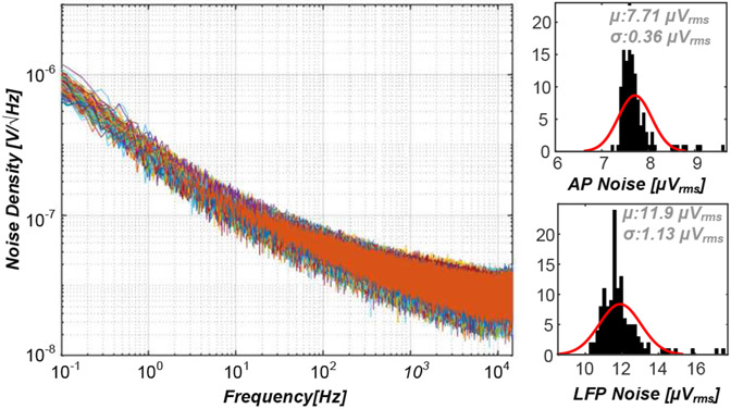
The measured input-referred noise spectrum of the 128 channels in a full bandwidth of 10 kHz are shown in Fig. 12 (left). This was measured by connecting the inputs of all the channels to ground. The histograms of the total input-referred integrated noise in the LFP (0.5 Hz - kHz) and AP (300 Hz - 10 kHz) frequency bands are shown in Fig. 12 (right). The mean LFP noise is 11.90 ± 1.13 , while the mean AP noise is 7.71 ± 0.36 . A good channel-to-channel noise uniformity is observed in this measurement. Table II summarizes the estimated AP-noise partitioning of the channel based on our post-layout simulation results. The main noise contribution (97%) comes from the stage. Both the AP and LFP noise performances of our NRIC are within the acceptable levels of the application, and similar to other widely used neural recording tools [1], [3].
Fig. 12.
Measured input-referred noise spectra of the 128 channels (left) and histograms of the integrated AP and LFP noise across channels (right).
TABLE II.
AP Noise Partitioning per Channel
| Source | Estimated Noise a |
|---|---|
| Gm | |
| HPF | |
| IDAC | |
| Quant. Noise | |
| Total |
Estimated from post-layout simulation
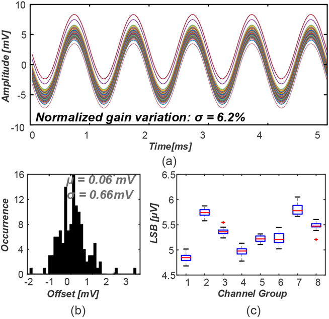
Figure 13 (a) shows the reconstructed transient waveforms of the 128 channels when a 1-kHz, 10-mVpp sinusoidal signal is applied to all the inputs. As can be observed, all the channels are fully functional and the gain variation across channels is 6.2% (). The channel offset is also extracted from the measured output waveforms and the histogram is shown in Fig. 13 (b). The mean offset is 0.09 ± 0.66 mV (, ). Since the channels are divided into 8 groups, each with an independent bias generator, a mismatch in the LSB of each channel group is expected. This is because the IDAC unit current is derived from the bias generator. To characterize this effect, the input-referred ADC LSB has been calculated for each channel from the measurements in Fig. 13 (c). The boxplot demostrates the distribution of LSB values for each channel group. It can be observed that the LSB variation in each group is very small, but the means across the 8 groups have a larger variation due to the mismatch between the 8 indepedent bias generators.
Fig. 13.
(a) Reconstructed transient output waveform for all the 128 channels. (b) Channel offset histogram. (c) Input-referred ADC LSB boxplot across all the channels in the 8 different channel groups.
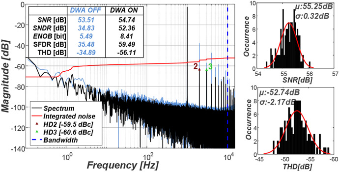
The measured output spectrum of one channel is shown in Fig. 14 (left). Here, a 1-kHz, 21.5-mVpp input sinewave is applied. The measured SNR, SNDR and THD are 54.74 dB, 52.36 dB and −56.11 dB, respectively, over a 10-kHz bandwidth. Fig. 14 (right) shows the histogram of the SNR and THD across all the 128 channels. The mean SNR is 55.25 ± 0.32 dB, while the mean THD is −52.74 ± −2.17 dB. A good channel-to-channel uniformity is observed here.
Fig. 14.
Left: channel spectrum analysis with a 21.5-mVpp, 1-kHz sinewave input, with and without DWA. Right: histograms of the SNR and THD across 128 channels.
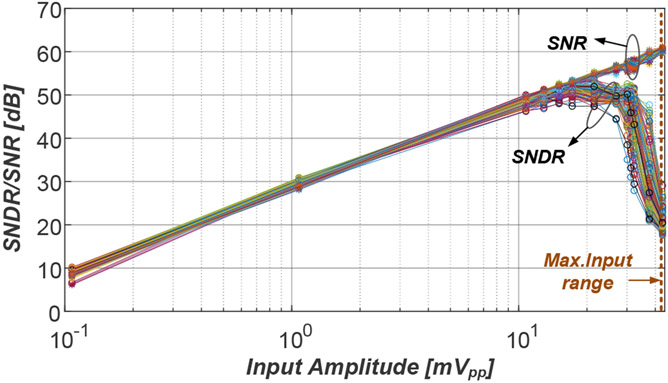
Figure 15 shows the measured SNR and SNDR versus input amplitude for a 1-kHz signal. The SNR and SNDR increase with the input amplitude until ~20 mVpp. Distortion starts to appear at large amplitudes due to the non-linearity of the stage (including the HPF) and the residual distortion of the IDAC caused by the non-idealities of the clock generator. However, the SNR keeps increasing until a maximum amplitude of 43 mVpp. Since extracellular neural signals have maximum amplitudes of 5-10 mVpp [55], the extended input range improves the tolerance to motion artifacts during in vivo neural recording. It is important to notice that the THD remains below −40 dB (1%) for input amplitudes of up to 30 mVpp, which is the acceptable non-linearity limit for this application.
Fig. 15.
Measured SNR and SNDR vs. input amplitude
B. In Vivo Measurement
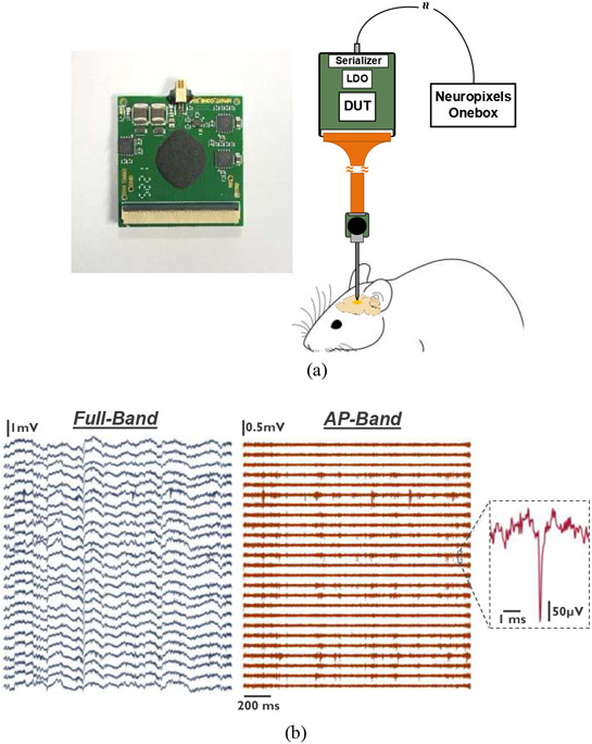
To enable in vivo experiments with the proposed NRIC, a small (2.5 × 2.5 cm2) and light (3.2 g) HS was built to provide connectivity to a computer (Fig. 16 (a) (left)). The HS consists of the NRIC, a serializer chip to transmit the data to a Neuropixels OneBox, LDO’s to generate the required supply voltages, an oscillator to generate the master clock (48 MHz), decoupling capacitors and connectors.
Fig. 16.
(a) Diagram of the setup for in vivo measurements. (b) Measured neural signals.
We have performed acute in vivo experiments to further demonstrate the complete functionality of the NRIC. For this, a passive probe with 128 TiN electrodes of diameter (impedance: 182.6 ± 21.4 kΩ @ 1 kHz) was implanted in the retrosplenial cortex of a C57Bl/6 J mouse. The animal was head-fixed while running on a treadmill. An illustration of the in vivo setup is shown in Fig. 16 (a) (right), while Fig. 16 (b) shows a 1.7-second extract of the recorded spontaneous activity in 25 channels. Both the full band and the software-filtered AP band are shown, demonstrating that the proposed architecture is able to record neural APs and LFPs [7].
C. Comparison with State-of-the-Art NRICs
Table III summarizes the features and measured performance of the proposed NRIC and compares them with recently-reported state-of-the-art neural readout architectures that cover both the LFP and AP frequency bands. Our design achieves one of the smallest areas (similar to [37]) and lowest power efficiency factors (PEFs). At the same time, our NRIC achieves rail-to-rail EDO cancellation, good noise performance and an improved input range compared to [2], [3], [13], [37]. The latter makes our design more suitable for recording experiments with freely-moving animals or in combination with near-by microstimulation. Although the AP noise is not as low as in [30], the performance is similar to [3] which is a well-established neurophysiology tool. The larger LFP noise is not a concern since LFP signals have much larger amplitudes than APs [55], and they are assessed by the power variation in the low-frequency range.
TABLE III.
Performance Summary and Comparison with Prior State-of-the-Art
| This work | Wang [30] | Yoon [13] | Wang [3] | Wendler [37] | De Dorigo [2] | Lee [31] | |
|---|---|---|---|---|---|---|---|
| Technology [nm] | 22 | 55 | 65 | 130 | 180 | 180 | 110 |
| Supply [V] | 0.8 | 1.2 | 1.2e | 1.2 | 1.8 | 1.8 | 1.0 |
| Topology | AC-coupled 1st order | DC-coupled 2nd order | AC-coupled, IA + SAR ADC | AC-coupled, IA + SAR ADC | DC-coupled, 2 Step, | DC-coupled | DC-coupled 2nd order |
| No.of Channels | 128 | 16 | 1024 | 384 | 8 | 144 | 1 |
| Area/Ch [mm2] | 0.0045 | 0.0077 | 0.0062 | 0.035 | 0.0046 | 0.0049 | 0.078c |
| Total area/Ch [mm2] | 0.0051 | 0.0298 | 0.02 | 0.0497 | - | - | 0.078c |
| AP Noise (0.3-10kHz) | 7.71±0.36 | 5.53±0.36 | 8.89b | 7.43±0.72 | 4.46/11.83f | 13.43 | 9.5 (1-10kHz) |
| LFP Noise (0.5HZ-1kHz) | 11.9±1.13 | 2.88±0.18 | 6.8b (5Hz-1kHz) | 7.78±0.93 | 2.51/9.21f | 9.95 | |
| Bandwidth [Hz] | 0.1-10k | 0.5-10k | 5-10k | 0.5-10k | 0.5-10k | 0.5-10k | 1-10k |
| Power/Ch | 6.02g | 61.2 | 2.72h | 45.3h | 14.62 | 39.14 | 6.5c |
| Total power/Ch | 12.57 | - | 24.08 | 95.1 | 25.75 | 46.08 | - |
| Channel PEFa (AP Band) | 54.55 | 285.28 | 33 | 381.2 | 306f | 1076.1 | 93.55c,d |
| Total PEFa (AP Band) | 113.9 | - | 290.09 | 800.26 | 539f | 1267 | - |
| THD | 0.15-0.41% @21.5mVpp | 0.05-0.44% @20mVpp | 0.57% @-0.79dBFS | 0.17% @10mVpp | 0.078%/1.24%f @10mVpp | 0.22% @10mVpp | 0.095% @285mVpp |
| AC Input Range [mVpp] | 43 | 148 | 0.75-4.87e | 12.5 | 14 | 22.5 | 300 |
| EDO Tolerance [mV] | Rail-to-Rail | ±70 | Rail-to-Rail | Rail-to-Rail | ±60 | <22.5 | ±50 |
PEF calculated by
No statistical data provided
Decimation filter not included
PEF with full bandwidth
Estimated
When a ±60mV offset appears in the input
Includes channel analog, DWA, decimation filter, up/down counter and adder (the last 2 are estimated from digital back-end)
Includes analog channel + ADC.
Differently from [13], the performance of our chip is fully characterized across all the channels. Our measurement results show a very good channel-to-channel uniformity, which is a crucial characteristic in high-channel-count neural interfaces. By combining AC-coupling, 1st-order noise shaping and digital processing, our design achieves an excellent compromise between the most important performance metrics for this application: area, power, noise, input range and EDO cancellation.
When compared to other designs (see Table IV), our design achieves the smallest area with competitive noise density and power/bandwidth. It is clear from the table that lower bandwidth designs [29], [34] are optimized to achieve very low noise and power at the expense of area. Although [21] achieves impressive noise and power performances in a large bandwidth, its area is too large to enable further channel-count scaling.
TABLE IV.
Comparison with Prior Architectures
| This work | Kassiri [29] | Reza [34] | Wang [30] | Park [21] | |
|---|---|---|---|---|---|
| Application | AP+LFP | ECoG | ECoG | AP+LFP | AP+LFP |
| No. of Channels | 128 | 64 | 32 | 16 | 128 |
| Technology[nm] | 22 | 130 | 130 | 55 | 180 |
| Supply[V] | 0.8 | 1.2 | 1.2 | 1.2 | 0.5/1.0 |
| Area/Ch [mm2] | 0.0045 | 0.013 | 0.023 | 0.0077 | 0.058 |
| Noise | 7.71 | 1.13b | 1.6 | 5.53 | 3.32 |
| Noise bandwidth [Hz] | 300-10k | 0.1-500 | 1-500 | 300-10k | 0.5-10.9k |
| Noise Density [nV/√Hz] | 78.28 | 50.54 | 71.63 | 56.15 | 31.80 |
| Channel Power | 6.02 | 0.63a | 1.7 | 61.2 | 3.05 |
| Bandwidth [Hz] | 0.1-10k | 0.01-500 | 1-500 | 0.5-10k | 0.5-10.9k |
| Power/Bandwidth [nW/Hz] | 0.62 | 1.26 | 3.41 | 6.31 | 0.28 |
| Channel PEF | 54.55 | 9.80 | 12.90 | 285.29 | 4.56 |
| Input Impedance [Ω] | ∞ @ DC | 99k-102kb | 1.47G @ DC | 663M @ 10Hz | ∞ @ DC |
| THD | 0.15-0.41% @21.5mVpp | - | - | 0.05-0.44% @20mVpp | 0.019% @3mVpp |
Decimation filter is not included
Calculated with OSR = 1000
V. Conclusion
To further increase the density of existing neural-recording tools, more area- and power-efficient readout architectures are needed. However, system co-optimization is crucial to ensure that other performance metrics such as noise, input range and electrode DC offset cancellation are also simultaneously achieved. We have reported an AC-coupled 1st-order architecture for the simultaneous acquisition of local field potentials and action potentials. To fully profit from the power and area benefits of the used scaled technology, we have pursued a digitally-intensive architecture with a novel combination of: i) AC-coupling for EDO rejection, ii) 1st-order noise shaping, iii) fully-digital feedback integrator (up-down counter) and feedback summation, iv) 2nd-order decimation, v) ultra-small bulk-regulated reference generator, vi) small-unit IDAC, and vii) DWA mismatch shaping. Because of these design choices, our design achieves one of the smallest channel areas compared with the state of the art, while also showing a very good compromise between all the above-mentioned metrics. We also demonstrated that the fabricated 128-channel prototype achieves a very good channel-to-channel uniformity, which is very important for ensuring good quality recording in high-density interfaces. The proposed digitally-intensive direct- digitization architecture holds the promise of enabling even higher density neural recording tools than those existing today.
Acknowledgment
The authors would like to thank Stefan Guns for the PCB and HS design, Andrea Lodi for the software GUI development, Joel Neys for the FPGA firmware development, Nils Van Geele for the API design, and Shahriar Hosseinjany for the help in in vivo data acquisition.
This research was partially supported by the NIH grant 1U01NS115587 (Neuropixels NXT).
Biographies

Xiaolin Yang (Member, IEEE) received the Ph.D. degree in circuits and systems from Zhejiang University, Hangzhou, China, in 2019. From 2017 to 2018, he was an International Scholar with Connected Health Solution Team, imec, Leuven, Belgium, where he worked on the high precision, high dynamic range front-end for bio-signal recording. In May 2019, he joined imec as Researcher and an Analog Circuits Engineer focused on neural interface circuits. He is currently a Senior Researcher and a Technical Leader of Neurotech team with imec. His research interests include analog and mixed-signal circuit design for bioelectronics, neural interfaces.

Marco Ballini (Member, IEEE) received the Ph.D. degree in electrical engineering from ETH Zürich. Zürich, Switzerland, in 2013. His Ph.D. work was focused on the design of CMOS-based microelectrode arrays. Following his Ph.D. degree, he has worked as an Analog IC Designer and a Senior Researcher with imec, Leuven, Belgium. In 2021, he joined TDK InvenSense, Milan, Italy, working as a System Design Engineer and an ASIC Architect (Senior Staff). His research interests include low-noise, low power, and small-area analog and mixed-signal circuits for sensors, bioelectronics, and neural interfaces.
Dr. Ballini is a member of Solid-State Circuits Society (SSCS) and Circuits and Systems (CAS). He serves as an Associate Editor for the IEEE OPEN JOURNAL OF CIRCUITS AND SYSTEMS

Chutham Sawigun (Member, IEEE) received the Ph.D. degree in analog IC design for biomedical applications from the Delft University of Technology, Delft, The Netherlands, in 2014. He was an Assistant Professor of analog electronics with the Mahanakorn University of Technology, Bangkok, Thailand. His research focused on ultra-low-power MOS ICs for biomedical applications. In 2019, he joined IMEC, Leuven, Belgium, where he is currently a Senior Researcher with Circuits for Neural Interfaces Group.

Wen-Yang Hsu received the M.S. degree in Electronics Engineering from National Tsing Hua University and the PhD degree from Swiss Federal Institute of Technology in Lausanne (EPFL) in 2011 and 2018, respectively. He has been a circuit designer with TSMC, BioPro Scientific, MediaTek and IMEC. Since 2023, he has been with Infinera, where he is involved in the design of multi-gigabit circuits for optical communication in advanced CMOS technology. His research interests include low-power, low-noise circuits and systems for biomedical application as well as high-speed interface.

Jan-Willem Weijers (Member, IEEE) was born in the Netherlands, in 1965. He received the degree of civil engineer microelectronics from KU Leuven, Belgium, in 1989. In 2000, he joined imec, as a Digital Design and Verification Engineer.

Jan Putzeys was with Imec in 2000 as a Characterization Engineer on cryogenic CMOS readout circuits for space applications. He has been developing dedicated test setups for low noise, low power readout electronics, and has designed readout systems for CCD and CMOS imagers.
He is currently involved in system design for neural readout ICs, with a focus on low power consumption and miniaturization.

Carolina Mora Lopez (Senior Member, IEEE) received the Ph.D. degree in electrical engineering from Katholieke Universiteit (KU) Leuven, Leuven, Belgium, in 2012, in collaboration with imec, Leuven. From 2012 to 2018, she worked as a Researcher and an Analog Designer with imec focused on interfaces for neural-sensing applications. She is currently the Principal Scientist and the Team Leader of the circuits for neural interfaces team with imec. Her research interests include analog and mixed-signal circuit design for sensors, bioelectronics, and neural interfaces.
Dr. Mora Lopez serves on the Technical Program Committee of the VLSI Circuits Symposium, International Solid-State Circuits Conference (ISSCC), and ESSCIRC conferences.
Footnotes
All animal procedures were approved by the Animal Ethics Committee of the KU Leuven, following the national guidelines on the use of laboratory animals (Belgian Royal Decree of 29 May 2013) and the European Union Directive for animal experiments (2010/63/EU).
Contributor Information
Xiaolin Yang, imec, Leuven, Belgium.
Marco Ballini, imec, Leuven, Belgium. He is now with TDK InvenSense, Milan, Italy..
Chutham Sawigun, imec, Leuven, Belgium.
Wen-Yang Hsu, imec, Leuven, Belgium.
Jan-Willem Weijers, imec, Leuven, Belgium.
Jan Putzeys, imec, Leuven, Belgium.
Carolina Mora Lopez, imec, Leuven, Belgium.
References
- [1].Mora Lopez C et al. , ‘A Neural Probe With Up to 966 Electrodes and Up to 384 Configurable Channels in 0.13 SOI CMOS’, IEEE Trans. Biomed. Circuits Syst, vol. 11, no. 3, pp. 510–522, Jun. 2017. [DOI] [PubMed] [Google Scholar]
- [2].De Dorigo D et al. , ‘Fully Immersible Subcortical Neural Probes With Modular Architecture and a Delta-Sigma ADC Integrated Under Each Electrode for Parallel Readout of 144 Recording Sites’, IEEE J. Solid-State Circuits, vol. 53, no. 11, pp. 3111–3125, Nov. 2018. [Google Scholar]
- [3].Wang S et al. , ‘A Compact Quad-Shank CMOS Neural Probe With 5,120 Addressable Recording Sites and 384 Fully Differential Parallel Channels’, IEEE Trans. Biomed. Circuits Syst, vol. 13, no. 6, pp. 1625–1634, 2019. [DOI] [PubMed] [Google Scholar]
- [4].Raducanu BC et al. , ‘Time Multiplexed Active Neural Probe with 1356 Parallel Recording Sites’, Sensors, vol. 17, no. 10, p. 2388, Oct. 2017. [DOI] [PMC free article] [PubMed] [Google Scholar]
- [5].Lopez CM et al. , ‘An Implantable 455-Active-Electrode 52-Channel CMOS Neural Probe’, IEEE J. Solid-State Circuits, vol. 49, no. 1, pp. 248–261, 2014. [Google Scholar]
- [6].Stevenson I, ‘Tracking Advances in Neural Recording’. [Online]. Available: https://stevenson.lab.uconn.edu/scaling/#. [Google Scholar]
- [7].Harrison RR and Charles C, ‘A low-power low-noise CMOS amplifier for neural recording applications’, Solid-State Circuits, IEEE J., vol. 38, no. 6, pp. 958–965, 2003. [Google Scholar]
- [8].Han Dong, Zheng Yuanjin, Rajkumar R, Dawe GS, and Je Minkyu, ‘A 0.45V 100-channel neural-recording IC with sub- consumption in CMOS’, IEEE Trans. Biomed. Circuits Syst, vol. 7, no. 6, pp. 735–746, 2014. [DOI] [PubMed] [Google Scholar]
- [9].Liu X et al. , ‘An artifact-suppressed stimulator for simultaneous neural recording and stimulation systems’, Proc. Annu. Int. Conf. IEEE Eng. Med Biol. Soc. EMBS, vol. c, pp. 2118–2121, 2017. [DOI] [PubMed] [Google Scholar]
- [10].Shulyzki R et al. , ‘320-Channel Active Probe for High-Resolution Neuromonitoring and Responsive Neurostimulation’, IEEE Trans. Biomed Circuits Syst, vol. 9, no. 1, pp. 34–49, 2015. [DOI] [PubMed] [Google Scholar]
- [11].Liu X et al. , ‘A Fully Integrated Wireless Compressed Sensing Neural Signal Acquisition System for Chronic Recording and Brain Machine Interface’, IEEE Trans. Biomed. Circuits Syst, vol. 10, no. 4, pp. 874–883, Aug. 2016. [DOI] [PubMed] [Google Scholar]
- [12].Lee T et al. , ‘A Multimodal Multichannel Neural Activity Readout IC with /Channel Ca2+-Probe-Based Fluorescence Recording and Electrical Recording’, in 2019 Symposium on VLSI Circuits, 2019, pp. C290–C291. [Google Scholar]
- [13].Yoon DY, Pinto S, Chung SW, Merolla P, Koh TW, and Seo D, ‘A 1024-Channel Simultaneous Recording Neural SoC with Stimulation and Real-Time Spike Detection’, in IEEE Symposium on VLSI Circuits, Digest of Technical Papers, 2021. [Google Scholar]
- [14].Gagnon-Turcotte G, Khiarak MN, Ethier C, De Koninck Y, and Gosselin B, ‘A CMOS SoC for Simultaneous Multichannel Optogenetics and Neural Recording’, IEEE J. Solid-State Circuits, vol. 53, no. 11, pp. 3087–3100, 2018. [Google Scholar]
- [15].Jung Y et al. , ‘A Wide-Dynamic-Range Neural-Recording IC With Automatic-Gain-Controlled AFE and CT Dynamic-Zoom ADC for Saturation-Free Closed-Loop Neural Interfaces’, IEEE J. Solid-State Circuits, pp. 1–12, 2022. [Google Scholar]
- [16].Bagheri A, Salam MT, Perez Velazquez JL, and Genov R, ‘Low-Frequency Noise and Offset Rejection in DC-Coupled Neural Amplifiers: A Review and Digitally-Assisted Design Tutorial’, IEEE Trans. Biomed. Circuits Syst, vol. 11, no. 1, pp. 1–16, Feb. 2016. [DOI] [PubMed] [Google Scholar]
- [17].Muller R, Gambini S, and Rabaey JM, ‘A 0.013 mm2, , DC-Coupled Neural Signal Acquisition IC With 0.5 V Supply’, IEEE J. Solid-State Circuits, vol. 47, no. 1, pp. 232–243, Jan. 2012. [Google Scholar]
- [18].Muller R et al. , ‘A Minimally Invasive 64-Channel Wireless Implant’, IEEE J. Solid-State Circuits, vol. 50, no. 1, pp. 344–359, Jan. 2015. [Google Scholar]
- [19].Chandrakumar H and Markovic D, ‘A 15.2-ENOB 5-kHz BW W Chopped CT for artifact-tolerant neural recording front ends’, IEEE J. Solid-State Circuits, vol. 53, no. 12, pp. 3470–3483, 2018. [Google Scholar]
- [20].Biederman W et al. , ‘A fully-integrated, miniaturized (0.125 mm2) wireless neural sensor’, IEEE J. Solid-State Circuits, vol. 48, no. 4, pp. 960–970, 2013. [Google Scholar]
- [21].Park S-Y, Cho J, Na K, and Yoon E, ‘Modular 128-Channel Analog Front-End Architecture Using Spectrum Equalization Scheme for 1024-Channel 3-D Neural Recording Microsystems’, IEEE J. Solid-State Circuits, vol. 53, no. 2, pp. 501–514, Feb. 2018. [Google Scholar]
- [22].Lopez CM et al. , ‘22.7 A 966-electrode neural probe with 384 configurable channels in SOI CMOS’, in 2016 IEEE International Solid-State Circuits Conference (ISSCC), 2016, pp. 392–393. [Google Scholar]
- [23].Mora Lopez C et al. , ‘A Neural Probe With Up to 966 Electrodes and Up to 384 Configurable Channels in SOI CMOS’, IEEE Trans. Biomed Circuits Syst, vol. 11, no. 3, pp. 510–522, Jun. 2017. [DOI] [PubMed] [Google Scholar]
- [24].Jun JJ et al. , ‘Fully integrated silicon probes for high-density recording of neural activity’, Nature, vol. 551, no. 7679, pp. 232–236, Nov. 2017. [DOI] [PMC free article] [PubMed] [Google Scholar]
- [25].Steinmetz NA et al. , ‘Neuropixels 2.0: A miniaturized high-density probe for stable, long-term brain recordings’, Science (80-. )., vol. 372, no. 6539, p. eabf4588, 2021. [DOI] [PMC free article] [PubMed] [Google Scholar]
- [26].Fathy NSK, Huang J, and Mercier PP, ‘A Digitally Assisted Multiplexed Neural Recording System With Dynamic Electrode Offset Cancellation via an LMS Interference-Canceling Filter’, IEEE J. Solid-State Circuits, vol. 57, no. 3, pp. 1–12, 2021. [Google Scholar]
- [27].Sharma M et al. , ‘Acquisition of Neural Action Potentials Using Rapid Multiplexing Directly at the Electrodes’, Micromachines 2018, Vol. 9, Page 477, vol. 9, no. 10, p. 477, 2018. [DOI] [PMC free article] [PubMed] [Google Scholar]
- [28].Pazhouhandeh MR, Kassiri H, Shoukry A, Wesspapir I, Carlen P, and Genov R, ‘Artifact-Tolerant Opamp-Less Delta-Modulated Bidirectional Neuro-Interface’, IEEE Symp. VLSI Circuits, Dig. Tech. Pap., vol. 2018-June, pp. 127–128, 2018. [Google Scholar]
- [29].Kassiri H et al. , ‘Rail-to-Rail-Input Dual-Radio 64-Channel Closed-Loop Neurostimulator’, IEEE J. Solid-State Circuits, vol. 52, no. 11, pp. 1–18, 2017. [Google Scholar]
- [30].Wang S et al. , ‘A Compact Chopper Stabilized Neural Readout IC With Input Impedance Boosting’, IEEE Open J. Solid-State Circuits Soc, vol. 1, no. June, pp. 67–78, 2021. [Google Scholar]
- [31].Lee C et al. , ‘A 10-kHz BW 80.4-dB SNDR -C-Based CT Modulator With a Feedback-Assisted Linearization for Artifact-Tolerant Neural Recording’, IEEE J. Solid-State Circuits, vol. 60, no. 3, pp. 1–1, 2020. [Google Scholar]
- [32].Nikas A, Jambunathan S, Klein L, Voelker M, and Ortmanns M, ‘A Continuous-Time Delta-Sigma Modulator Using a Modified Instrumentation Amplifier and Current Reuse DAC for Neural Recording’, IEEE J. Solid-State Circuits, vol. 54, no. 10, pp. 2879–2891, 2019. [Google Scholar]
- [33].Jeon H, Bang JS, Jung Y, Choi I, and Je M, ‘A High DR, DC-Coupled, Time-Based Neural-Recording IC with Degeneration R-DAC for Bidirectional Neural Interface’, IEEE J. Solid-State Circuits, vol. 54, no. 10. pp. 2658–2670, 2019. [Google Scholar]
- [34].Reza Pazhouhandeh M, Chang M, Valiante TA, and Genov R, ‘Track- and-Zoom Neural Analog-to-Digital Converter With Blind Stimulation Artifact Rejection’, IEEE J. Solid-State Circuits, vol. 55, no. 7, pp. 1984–1997, Jul. 2020. [Google Scholar]
- [35].Pazhouhandeh MR, Kassiri H, Shoukry A, Weisspapir I, Carlen PL, and Genov R, ‘Opamp-Less /Channel -Modulated Neural-ADC With Super-GΩ Input Impedance’, IEEE J. Solid-State Circuits, vol. 56, no. 5, pp. 1565–1575, May 2021. [Google Scholar]
- [36].Huang X et al. , ‘A 256-Channel Actively-Multiplexed uECoG Implant with Column-Parallel Incremental ADCs Employing Bulk-DACs in 22-nm FDSOI Technology’, in 2022 IEEE International Solid-State Circuits Conference (ISSCC), 2022, vol. 65, pp. 200–202. [Google Scholar]
- [37].Wendler D et al. , ‘A 0.0046-mm2 Two-Step Incremental Delta-Sigma Analog-to-Digital Converter Neuronal Recording Front End With 120-mVpp Offset Compensation’, IEEE J. Solid-State Circuits, pp. 1–12, 2022. [Google Scholar]
- [38].Kim C, Joshi S, Courellis H, Wang J, Miller C, and Cauwenberghs G, ‘-Noise /Channel ADC-Direct Neural Recording With 200-mV/ms Transient Recovery Through Predictive Digital Autoranging’, IEEE J. Solid-State Circuits, vol. PP, pp. 1–10, 2018. [Google Scholar]
- [39].a Smith W, Uehlin JP, Perlmutter SI, Rudell JC, and Sathe VS, ‘A scalable, highly-multiplexed delta-encoded digital feedback ECoG recording amplifier with common and differential-mode artifact suppression’, in 2017 Symposium on VLSI Circuits, 2017, pp. C172–C173. [Google Scholar]
- [40].Han M et al. , ‘Bulk switching instrumentation amplifier for a high-impedance source in neural signal recording’, IEEE Trans. Circuits Syst. II Express Briefs, vol. 62, no. 2, pp. 194–198, 2015. [Google Scholar]
- [41].Tu C, Wang Y, and Lin T, ‘A Low-Noise Area-Efficient Chopped VCO-Based CTDSM for Sensor Applications in 40-nm CMOS’, IEEE J. Solid-State Circuits, vol. 52, no. 10, pp. 2523–2532, Oct. 2017. [Google Scholar]
- [42].Huang J et al. , ‘A 0.01-mm 2 Mostly Digital Capacitor-Less AFE for Distributed Autonomous Neural Sensor Nodes’, IEEE Solid-State Circuits Lett., vol. 1, no. 7, pp. 162–165, Jul. 2018. [Google Scholar]
- [43].Johnson BC et al. , ‘An implantable 64-channel neuromodulation IC for simultaneous recording and stimulation with rapid artifact recovery’, in 2017 Symposium on VLSI Circuits, 2017, pp. C48–C49. [Google Scholar]
- [44].Jiang W, Hokhikyan V, Chandrakumar H, Karkare V, and Marković D, ‘A ±50-mV Linear-Input-Range VCO-Based Neural-Recording Front-End With Digital Nonlinearity Correction’, IEEE J. Solid-State Circuits, vol. 52, no. 1, pp. 173–184, 2017. [Google Scholar]
- [45].Yang X, et al. ‘A 128-Channel AC-Coupled 1st-order IC for Neural Signal Acquisition’, in 2022 IEEE Symposium on VLSI Technology and Circuits (VLSI Technology and Circuits), 2022, pp. 60–61. [Google Scholar]
- [46].Sukumaran A and Pavan S, ‘Low Power Design Techniques for Single-Bit Audio Continuous-Time Delta Sigma ADCs Using FIR Feedback’, IEEE J. Solid-State Circuits, vol. 49, no. 11, pp. 2515–2525, 2014. [Google Scholar]
- [47].Pavan S, Schreier R, and Temes GC, Understanding Delta-Sigma Data Converters. John Wiley & Sons, Ltd, 2017. [Google Scholar]
- [48].Carvajal RG et al. , ‘The flipped voltage follower: a useful cell for low-voltage low-power circuit design’, IEEE Trans. Circuits Syst. I Regul. Pap, vol. 52, no. 7, pp. 1276–1291, 2005. [Google Scholar]
- [49].Van Elzakker M, Van Tuijl E, Geraedts P, Schinkel D, Klumperink E, and Nauta B, ‘A 4.4fJ/conversion-step 10b 1MS/S charge-redistribution ADC’, in Digest of Technical Papers - IEEE International Solid-State Circuits Conference, 2008. [Google Scholar]
- [50].de la Rosa JM, ‘Sigma-Delta Modulators: Tutorial Overview, Design Guide, and State-of-the-Art Survey’, IEEE Trans. Circuits Syst. I Regul. Pap, vol. 58, no. 1, pp. 1–21, 2011. [Google Scholar]
- [51].Cherry JA and Snelgrove WM, ‘Excess loop delay in continuous-time delta-sigma modulators’, IEEE Trans. Circuits Syst. II Analog Digit. Signal Process, vol. 46, no. 4, pp. 376–389, Apr. 1999. [Google Scholar]
- [52].Banba H et al. , ‘A CMOS band-gap reference circuit with sub 1 V operation’, in 1998 Symposium on VLSI Circuits. Digest of Technical Papers (Cat. No.98CH36215), 1998, pp. 228–229. [Google Scholar]
- [53].Seok M, Kim G, Blaauw D, and Sylvester D, ‘A Portable 2-Transistor Picowatt Temperature-Compensated Voltage Reference Operating at 0.5 V’. IEEE J. Solid-State Circuits, vol. 47, no. 10, pp. 2534–2545, 2012. [Google Scholar]
- [54].Sawigun C, Yang X, Lodi A, and Lopez CM, ‘A scalable sub-nW nMOS voltage reference with multi-loop regulation achieving 0.0126%/V line sensitivity’, in 2022 IEEE Asian Solid-State Circuit Conference, p. (In press). [Google Scholar]
- [55].Mora Lopez C et al. , ‘A Multichannel Integrated Circuit for Electrical Recording of Neural Activity, With Independent Channel Programmability’, IEEE Trans. Biomed. Circuits Syst, vol. 6, no. 2, pp. 101–110, 2012. [DOI] [PubMed] [Google Scholar]


