

Abstract
We demonstrate a deterministic Purcell-enhanced single photon source realized by integrating an atomically thin WSe2 layer with a circular Bragg grating cavity. The cavity significantly enhances the photoluminescence from the atomically thin layer, and supports single photon generation with g(2)(0)<0.25. We observe a consistent increase of the spontaneous emission rate for WSe2 emitters located in the center of the Bragg grating cavity. These WSe2 emitters are self-aligned and deterministically coupled to such a broadband cavity, configuring a new generation of deterministic single photon sources, characterized by their simple and low–cost production and intrinsic scalability.
Keywords: two-dimensional materials, quantum dots, bullseyes cavities, single photons, Purcell effect
Graphical Abstract
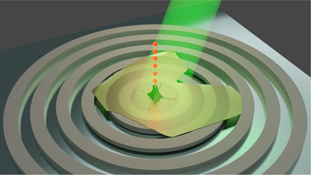
Representation of a bullseye grating cavity, with a nanopillar in the centre; an atomically thin monolayer of WSe2 is deposited on top. The local strain around the nanopillar forms a WSe2 quantum dot, coupled to the cavity. A green laser excites the quantum dot, emitting single photons efficiently.
INTRODUCTION
Advancing on the development of deterministic single photon sources for quantum optical applications requires engineering new devices with reduced complexity in both production and operation. The benchmarking performance for deterministic quantum sources of light is brightness, single photon purity, and photon coherence (indistinguishability) [1]. At the moment, and following these criteria, the leading technology is self-assembled InAs quantum dots (QDs) which are integrated either in monolithic [2–4], or open cavities [5]. The success of a particular single photon source technology depends not only on performance criteria but also on the affordability, simple manufacturability, and reproducibility of the device and its compatible integration with other pre-existing photonic technologies. In this sense, semiconductor QDs - while providing the current state-of-the-art performance as single photon sources - are arguably scalable [6,7] and constitute a resource-demanding technology, restricted to few specialized research groups around the globe. This imposes a significant barrier to ensure a broad, and fast impact of this solid-state-based single photon technology in a short time-scale, both for quantum applications, as well as for academic research.
Recently, a promising single photon emitter platform emerged from two-dimensional (2D) materials. Seminal work has demonstrated that localized excitons in monolayers (MLs) of transition metal dichalcogenides (TMDCs) can deliver single photons under a continuous wave, and pulsed excitation [8–12]. TMDC QDs can be controllably created using strain [13,14], enabling ordered arrays of TMDC QDs [14,15]. In principle, such method allows the scalable and deterministic integration of TMDC QDs in photonic micro- and nanostructures, which may be used for improving the emitter performance as single photon sources. Recently, the deterministic coupling of TMDC quantum emitters to plasmonic nanostructures was reported [16–19]. While the broadband nature of plasmonic approaches, in conjunction with the strong field enhancement makes this approach suitable for the integration of WSe2 sheets, it remains a complicated task to fully suppress undesired Ohmic losses in plasmonic implementations. Open microcavities based on conventional Bragg mirrors have been utilized to demonstrate the weak coupling regime between a WSe2 QD and a cavity mode [20]. However, this implementation, despite its flexibility in spectral tuning, presents challenges for applications that require large-scale TMDC QD integration or lab-independent user-friendliness.
An ideal cavity platform features a broad bandwidth operation with a large Purcell enhancement. This is accomplished when the cavity has simultaneously a moderate cavity quality factor (providing the large bandwidth) and a small mode volume (enhancing the resulting Purcell factor). Different types of photonic structures, which are compatible with the integration of atomically thin sheets, are naturally compatible with this goal, including photonic crystal cavities [22] and cavities consisting of a circular disk surrounded by a set of concentric rings in the thin membrane. The latter are known in the literature as Circular Bragg grating Bullseye cavities (CBGBs). CBGBs are especially interesting due to their simple design as well as being able to access different emission wavelengths in the range of 600 nm to 1500 nm with small modifications. Besides, they can be designed to specifically maximize the electromagnetic cavity field at the cavity–air interface, where the TMDC QD is positioned [23].
In this work, we implement a hybrid CBGB composed of an Al0.31Ga0.69As membrane, whose cavity mode couples to a WSe2 monolayer QD. These QDs are strain-defined in the monolayer by selectively grown nanopillars, centered in the CBGB. We demonstrate a spontaneous emission enhancement from the WSe2 QD photoluminescence by more than a factor of five. Moreover, we prove the single photon character of this emission by performing a second-order correlation measurement, revealing a strongly suppressed multiphoton emission.
DEVICE DESIGN AND FABRICATION
The CBGB geometry can support an optical resonance with a number of desirable features for creating single photon sources based on quantum emitters: efficient and preferentially vertical single photon emission with small divergence, relatively broad spectral operation for Purcell radiative rate enhancement factors exceeding 10. Here, Finite Difference Time Domain (FDTD) simulations were used to design a CBGB that would support such resonance in the 700 nm wavelength band. Figure 1a) shows a schematic of our CBGB structure, and Fig. 1b) shows a scanning electron microscope (SEM) image of a fabricated cavity. The geometry is composed of five concentric rings, with a nominal gap width of 100 nm and period of 350 nm, including a nominal 250 nm non-etched SiO2 slab. The inner/outer ring diameter is 1.6/5.1 μm, respectively. The CBGB with parameters as in 1a) supports a resonance at 748 nm that displays a strongly directive far field, as shown in Fig. 1c), optimal for collection with low numerical aperture optics, and hence constituting an efficient light-matter interface. Due to the lower refractive index contrast from the membrane to the SiO2 substrate, as compared to the air interface, the field preferentially extends into the substrate, however is reflected by the Au layer. The thickness of the SiO2 is optimized to maximize the extraction efficiency out of the sample.
Fig 1.
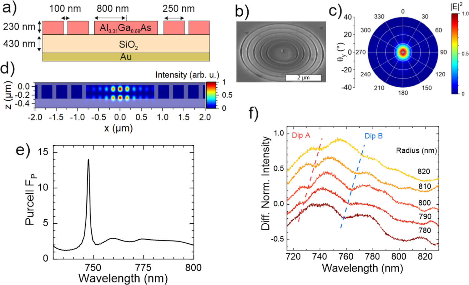
a) Schematic of the structure in a vertical cut. b) SEM image of a processed CBGB with a ≈ 200 nm pillar placed right in the centre, the white bar indicates 2 μm. c) FDTD far field calculation of the electric field for a dipole placed in the centre for the structure, showing an emission with a narrow angular dispersion (<10°). d) FDTD simulation of the electric field in a vertical cut along the CBGB diameter. The photonic mode is mainly confined in the central disk. e) Simulation of the Purcell enhancement versus wavelength for the previously described CBGB. f) Measured reflectivity as a function of wavelength on the finalized sample varying the nominal innermost radius (from 780 nm to 820 nm, see legend inside the panel). The spectral position of dip A and B are highlighted with dashed lines. This incremental variation reveals two modes in the range of 730 nm to 765 nm, which red-shift as a function of increasing radius.
Figure 1(d) shows that the modal field is strongly confined in the AlGaAs slab, and within the inner radius of the circular grating (Fig. S1). Importantly, the thickness of the AlGaAs membrane was chosen so that it would support a second-order transverse-electric (TE2) slab waveguide mode, with two vertical maxima, from which the bullseye cavity mode could be formed (see Fig. 1(d) and Fig. S2). The longer evanescent tail of the TE2 slab mode results in a cavity mode with a higher intensity above the AlGaAs slab, and therefore an improved coupling efficiency to emitters located at the surface of the structures. Cavities in which the fundamental (TE1) slab mode is used to form a bullseye resonance offer lower coupling to emitters at the surface, and are better suited for emitters located at the slab center. To estimate the maximum achievable Purcell radiative rate enhancement factor Fp for an emitter located at the CBGB surface, we simulated the emission of a horizontally oriented electric dipole located 10 nm above the AlGaAs, at the bullseye center. Figure 1(e) shows the Purcell enhancement factor Fp (calculated as the total dipole-emitted power normalized by the free-space dipole emitted power) as a function of emission wavelength. Purcell factors as large as 14 can be theoretically obtained within a bandwidth of a few nm. In Suppl. Section 8, we amend a deeper discussion of the impact of the nanopillar and the dipole orientation on the performance of the CBGB structure.
Fabrication of our CBGB structure starts from an epitaxially grown 230 nm thick Al0.31Ga0.69As membrane. The membrane is bonded via the “flip-chip” method on ≈430 nm thick layer of SiO2, on top of a ≈150 nm Au mirror, and a standard GaAs substrate. Details on the bonding procedure can be found in Ref. [24]. In the next steps, high-resolution electron-beam lithography and a subsequent lift-off process are used to prepare the pattern of the CBGBs. The pattern is transferred to the semiconductor membrane using reactive ion etching with an Ar/Cl2 plasma. To induce a QD “seed”, we apply a local electron beam deposition method in a FIB to grow a ≈200 nm tall SiO2 nanopillar accurately in the center of the cavity, utilizing a precursor gas (Si(C2H5O)4). This pillar serves to induce the WSe2 QD via local strain (see Supplementary S2 for further details on the nanopillar processing).
The single photon sources are finalized by the deposition of a monolayer of WSe2. These monolayers are exfoliated from a bulk crystal and transferred with a polymer (PDMS) stamp onto the device [25]. To enhance the adhesion of the monolayer to the CBGB, the stamping procedure was conducted at a temperature of 150 °C.
RESULTS AND DISCUSSION
Reflectivity measurements were performed in the fabricated structures to identify the spectral location of the CBGB resonant modes. Figure 1f) shows the white-light reflectivity spectra of CBGBs with nominal inner disk radius varying from 780 nm to 820 nm (other parameters were fixed), normalized to that of a silver surface. Two dips, labeled A and B, are systematically observed and, as highlighted with dashed lines, red-shift with increasing inner disc diameter. Dips A and B display bandwidths of ≈ 20 nm and ≈ 30 nm, corresponding to a quality factor of ≈40 and ≈30 respectively, and spectrally overlap with the typical energy emission of WSe2 QDs (between720 nm and 780 nm). Reflectivity spectra obtained from FDTD simulations, shown in Fig. S3, reveal dips in good qualitative agreement with the experiment, displaying similar bandwidths and spectral positions. As evident in the simulations, the desired CBGB cavity mode displaying the strong Purcell enhancement (Fig 1e) falls within the extent of dip A for all considered inner disk radii.
To facilitate a global characterization of quantum emitter coupling to our structures, we selected particularly large WSe2 monolayers on our PDMS stamp, with sizes of several tens of microns. Using flakes of that size, a single monolayer covers various CBGBs. In Fig. 2a) we present an optical microscope image of such a monolayer, which covers 4 CBGBs (the yellow line indicates the borders of the monolayer as a guide to the eye). In fig 2b), the close-up SEM image verifies that the nanopillar in the cavity center produces a nanometric “tent”, locally straining the monolayer, and so, producing single-excitonic emitters (WSe2 QDs) [15]. We reveal these single-excitonic sharp energy transitions by studying their micro-photoluminescence at cryogenic temperatures (4K) in a helium flow cryostat. The cryostat is mounted on a set of closed-loop X-Y translation stages, which allows performing two-dimensional scans with a minimum spatial resolution of ≈100 nm.
Fig. 2.
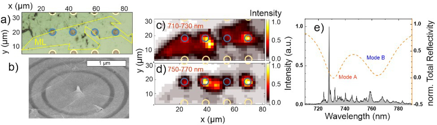
a) Microscope image the transferred monolayer (its limits are highlighted with a yellow line as a guide to the eye), covering several CBGBs with an inner radius of 800 nm (these cavities are highlighted with open blue circles). b) SEM image of a transferred WSe2 monolayer placed on the centre of a CBGB. The pillar is fully covered by the monolayer, some monolayer wrinkles are visible. c) and d) Photoluminescence intensity scans of the monolayer shown in panel a), integrating the energy mission in the spectral range 710 nm to 730nm and 750 nm to 770 nm, respectively. The emission is enhanced in the centre of each CBGB. e) Spectrum of one of the CBGBs shown in b). The simulated CBGB reflectivity is shown on the right axis, observing the spectral location of dip A and B. The spectral position of the dominant line at 728 nm coincides with the position of dip A. The sharp lines are photoluminescence features of the WSe2 QDs.
We record hyperspectral maps of the sample by scanning the sample position in steps of ≈2 μm while exciting the structure non-resonantly with a 532 nm laser (≈12 W/cm2) to capture the inter-dependence between luminescence intensity, sample position, and spectral window of interest. Figures 2c,d) show a photoluminescence map resulting from the scan of the 4 devices; these scans integrate the energy emission from 710 nm to 730 nm and 750 nm to 770 nm, respectively. The positions of the covered CBGBs are schematically highlighted with blue circles.
In Fig. 2c), we notice that in this spectral range 710 nm to 730 nm, apart from the sharp QD emission features, the WSe2 luminescence is characterized by the free exciton and the free trion band (in the Supplementary information Fig. S4 we show a spectrum outside of the CBGB for the sake of comparison). As a result, significant photoluminescence is observed over the entire monolayer area. Enhancement of the luminescence at the positions of the CBGBs occurs in this spectral range, indicating a coupling with cavity resonance ‘A’. In Fig. 2d) in contrast the background luminescence from the WSe2 monolayer is strongly reduced in the 750 nm to 770 nm range, spectrally aligned with reflectivity dip B. The photoluminescence intensity here almost exclusively arises from the cavity positions. This shows that the CBGBs are capable of efficiently redirecting single photon emission towards our collection optic. It is worth noting, however, that Purcell-enhanced emitters are expected to be spectrally aligned with dip A, as discussed previously.
A typical photoluminescence spectrum from one of the CBGBs is shown in Fig. 2e). The nanopillar yields the emergence of a variety of sharp emission features, which occur in the spectral region between 720 nm and 800 nm and which we associate with the formation of WSe2 QDs. The reflectivity spectrum fit for a representative CBGB with the same parameters is also plotted. Enhanced emission at 730 nm, spectrally aligned with reflectivity dip A, suggests the possibility of an acceleration of the spontaneous emission of this emitter via the Purcell effect. This effect is also reflected in a comparison of the power dependent photoluminescence of several emitters from different positions on the flake, indicating a higher saturated brightness for emitters on the CBGB (see Supplement Fig. S5).
To verify the single photon character of the investigated CBGBs, a second-order correlation experiment is performed on one of the intense, sharp emission lines (see Supp. S6, where the corresponding filtered spectral line is highlighted with a gray band). Figure 3a) shows the normalized second-order correlation function g(2)(τ) histogram under continuous-wave excitation. The strong reduction of the simultaneous coincidence events at zero delay proves the population suppression of multi-photon Fock states in the emission, and a predominant generation of single photons. The mono-exponential fit in Fig. 3a) shows a g(2)(0)=0.25(5), which puts our emitter clearly in the class of a single photon source. Further examples of single photon emitters are shown in Suppl. Fig S9.
Fig. 3.
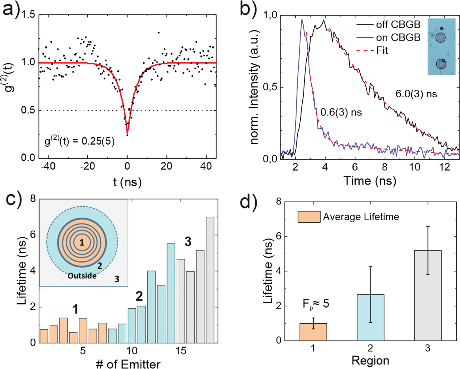
a) Second-order correlation measurement from a selected spectral line (shown in the supplementary) in a CBGB. b) Normalised lifetime measurement on (blue) and off (grey) the CBGB. The values 0.6(3) and 6.0(3) ns indicate the extracted lifetime of the transitions, respectively. Uncertainties in a) and b) are 95 % confidence intervals from the fits, corresponding to two standard deviations. c) Histogram of 18 individual emitters located in the monolayer, sorted by their position: 1) inside the inner disk 2) in the outer limit of the CBGB border, and 3) outside the CBGB device. The lifetimes in the region 1 (orange) are close to the detector resolution (≈350 ps), in contrast to emitters outside of the device (grey bars). d) Average lifetime for emitters within each of the regions defined in c). Fp is the estimated average Purcell enhancement for emitters in region 1, relative to emitters in region 3. Error bars correspond to the Student’s t-distribution 95 % confidence interval for each region.
We now study the spontaneous emission acceleration experienced by cavity-coupled WSe2 emitters. As the cavity bandwidth is too broad to study the same emitter on- and off-resonance by applying an external tuning knob (such as temperature or mechanical stress), we perform comparative measurements of WSe2 emitters emerging spatially inside and outside the cavities. The lifetime measurements are performed with a frequency-doubled Titanium Sapphire laser providing pulses of ≈2 ps at a wavelength of 448 nm with a repetition rate of 75 MHz. The single-photon detectors are silicon APDs presenting a time resolution of ≈350 ps.
Figure 3b) shows the normalized decay curves of two emitters located inside (blue curve) and outside (black curve) the CBGB. Each data set is fitted with a mono-exponential decay curve, yielding a characteristic decay time of 0.6(3) ns and 6.0(3) ns, respectively (uncertainties are 95 % confidence intervals from the fit, corresponding to two standard deviations). The difference in decay time suggests an accelerated spontaneous emission rate, with a Purcell enhancement of ≈10 for emitters efficiently coupled to the CBGB.
For a more quantitative analysis of this observation, in Fig. 3c) we subdivide the CBGB in three different concentric regions, numbered from 1 to 3, and we analyze the lifetime of 18 emitters distributed in these regions. Notably, the acceleration of the emitter dynamics systematically occurs throughout our selected structures in region 1 which is restricted to the area inside of the CBGB, inside a circle of 5.1 μm diameter (in Suppl. Fig. S7 we additionally probe the correspondence of a good spectral overlap between the emitter and cavity with an expected accelerated spontaneous emission). Region 2 represents the outer CBGB rim, where the laser excitation spot (presenting a FWHM diameter of ~3 μm) is positioned in the rim of the outer ring (>2.6 μm away from the center of the CBGB). Emitters in region 3 are clearly outside of the CBGB. The resulting histogram of the average lifetime as a function of the region, see Fig. 3d), reveals that the emitters located in the region 1 consistently experience a short lifetime of (1.0 ± 0.3) ns, whereas the lifetimes in region 2 and 3 displays a lifetime of (2.7 ± 1.4) ns and (5.2 ± 1.9) ns, respectively (reported lifetimes here correspond to the sample mean for each region, and uncertainties are the corresponding Student’s t-distribution 95 % confidence interval). Assuming that a WSe2 emitter on the plain AlGaAs surface (uncoupled to a CBGB) does not experience any modification of its spontaneous emission, this analysis determines a Purcell factor of up to ≈5 in these CBGB structures.
It is worth noting that, in contrast with previous reports on lifetime acceleration of WSe2 emitters using metallic nanostructures, the emergence of non-radiative losses due to the presence of dielectric nanopillars is less likely to play a critical role in the observed phenomena. WSe2 quantum emitters induced by polymer- or silicon nanopillars without the presence of CBGB structures have consistently been reported to feature spontaneous emission lifetimes in the range of 3 ns to 8 ns, consistent with those for emitters within region 3 in Fig. 1c) [14,15]. This strongly suggests that observed phenomenon of lifetime reduction in our work can be attributed to the enhancement of spontaneous emission in the weak coupling regime between the WSe2 QD and the CBGB.
CONCLUSION
To conclude, we have implemented a deterministically coupled, strain engineered single photon source by integrating a WSe2 QD in a circular Bragg grating Bullseye cavity. Our cavities provide a strong enhancement of spontaneous emission from WSe2 quantum emitters, and thus, our studies systematically demonstrate the first prototype of a monolithically coupled, cavity-enhanced single photon source, based on a two-dimensional material. We believe that the performance of our devices can be further improved by utilizing resonant excitation and combining the cavity with other external knobs such as mechanical strain [26] or electric control of the QD environment [11].
Supplementary Material
ACKNOWLEDGMENTS
We gratefully acknowledge support by the State of Bavaria. This work has been supported by European Research Council within the Project unLiMIt-2D (Project No. 679288) and by the German Research Association within the project PR1749 1–1. C.S. acknowledges fruitful discussions and creative input by R. Trotta and A. Predojevic as well as support by P. Pertsch and Prof. B. Hecht, University of Würzburg, for assisting within the dry stamping procedure. C.S. acknowledges the help of S. Kuhn, who carried out the lithography process, and M. Emmerling, who took the SEM images. S.T acknowledges support from DOE-SC0020653, NSF CMMI 1933214, NSF mid-scale 1935994, NSF 1904716, NSF DMR 1552220 and DMR 1955889.
Footnotes
ASSOCIATED CONTENT
Supporting Information
The Supporting Information contains expanded results about: (i) simulations and images of the CBGB devices, (ii) spectra and pump power dependences of coupled and un-coupled quantum emitters to the cavity, (iii) supplementary examples of anti-bunched two-photon correlation histograms from several quantum emitters. This material is available free of charge via the internet at http://pubs.acs.org.
REFERENCES
- [1].Senellart P, Solomon G, and White A, High-Performance Semiconductor Quantum-Dot Single-Photon Sources, Nat. Nanotechnol. 12, 1026 (2017). [DOI] [PubMed] [Google Scholar]
- [2].Unsleber S, He Y-M, Gerhardt S, Maier S, Lu C-Y, Pan J-W, Gregersen N, Kamp M, Schneider C, and Höfling S, Highly Indistinguishable On-Demand Resonance Fluorescence Photons from a Deterministic Quantum Dot Micropillar Device with 74% Extraction Efficiency, Opt. Express 24, 8539 (2016). [DOI] [PubMed] [Google Scholar]
- [3].Somaschi N, Giesz V, De Santis L, Loredo JC, Almeida MP, Hornecker G, Portalupi SL, Grange T, Antón C, Demory J, Gómez C, Sagnes I, Lanzillotti-Kimura ND, Lemaítre A, Auffeves A, White AG, Lanco L, and Senellart P, Near-Optimal Single-Photon Sources in the Solid State, Nat. Photonics 10, 340 (2016). [Google Scholar]
- [4].Ding X, He Y, Duan Z-C, Gregersen N, Chen M-C, Unsleber S, Maier S, Schneider C, Kamp M, Höfling S, Lu C-Y, and Pan J-W, On-Demand Single Photons with High Extraction Efficiency and Near-Unity Indistinguishability from a Resonantly Driven Quantum Dot in a Micropillar, Phys. Rev. Lett. 116, 020401 (2016). [DOI] [PubMed] [Google Scholar]
- [5].Tomm N, Javadi A, Antoniadis NO, Najer D, Löbl MC, Korsch AR, Schott R, Valentin SR, Wieck AD, Ludwig A, and Warburton RJ, A Bright and Fast Source of Coherent Single Photons, Nat. Nanotechnol. (2021). [DOI] [PubMed] [Google Scholar]
- [6].He Y-M, Liu J, Maier S, Emmerling M, Gerhardt S, Davanço M, Srinivasan K, Schneider C, and Höfling S, Deterministic Implementation of a Bright, on-Demand Single-Photon Source with near-Unity Indistinguishability via Quantum Dot Imaging, Optica 4, 802 (2017). [DOI] [PMC free article] [PubMed] [Google Scholar]
- [7].Ollivier H, Wenniger I. Maillette de Buy, Thomas S, Wein SC, Harouri A, Coppola G, Hilaire P, Millet C, Lemaître A, Sagnes I, Krebs O, Lanco L, Loredo JC, Antón C, Somaschi N, and Senellart P, Reproducibility of High-Performance Quantum Dot Single-Photon Sources, ACS Photonics 7, 1050 (2020). [Google Scholar]
- [8].Srivastava A, Sidler M, Allain AV, Lembke DS, Kis A, and Imamoğlu A, Optically Active Quantum Dots in Monolayer WSe2, Nat. Nanotechnol. 10, 491 (2015). [DOI] [PubMed] [Google Scholar]
- [9].He Y-M, Clark G, Schaibley JR, He Y, Chen M-C, Wei Y-J, Ding X, Zhang Q, Yao W, Xu X, Lu C-Y, and Pan J-W, Single Quantum Emitters in Monolayer Semiconductors, Nat. Nanotechnol. 10, 497 (2015). [DOI] [PubMed] [Google Scholar]
- [10].Koperski M, Nogajewski K, Arora A, Cherkez V, Mallet P, Veuillen J-Y, Marcus J, Kossacki P, and Potemski M, Single Photon Emitters in Exfoliated WSe2 Structures, Nat. Nanotechnol. 10, 503 (2015). [DOI] [PubMed] [Google Scholar]
- [11].Chakraborty C, Kinnischtzke L, Goodfellow KM, Beams R, and Vamivakas AN, Voltage-Controlled Quantum Light from an Atomically Thin Semiconductor, Nat. Nanotechnol. 10, 507 (2015). [DOI] [PubMed] [Google Scholar]
- [12].Tonndorf P, Schmidt R, Schneider R, Kern J, Buscema M, Steele GA, Castellanos-Gomez A, van der Zant HSJ, Michaelis de Vasconcellos S, and Bratschitsch R, Single-Photon Emission from Localized Excitons in an Atomically Thin Semiconductor, Optica 2, 347 (2015). [Google Scholar]
- [13].Kumar S, Kaczmarczyk A, and Gerardot BD, Strain-Induced Spatial and Spectral Isolation of Quantum Emitters in Mono- and Bilayer WSe 2, Nano Lett. 15, 7567 (2015). [DOI] [PMC free article] [PubMed] [Google Scholar]
- [14].Palacios-Berraquero C, Kara DM, Montblanch AR-P, Barbone M, Latawiec P, Yoon D, Ott AK, Loncar M, Ferrari AC, and Atatüre M, Large-Scale Quantum-Emitter Arrays in Atomically Thin Semiconductors, Nat. Commun. 8, 15093 (2017). [DOI] [PMC free article] [PubMed] [Google Scholar]
- [15].Branny A, Kumar S, Proux R, and Gerardot BD, Deterministic Strain-Induced Arrays of Quantum Emitters in a Two-Dimensional Semiconductor, Nat. Commun. 8, 1 (2017). [DOI] [PMC free article] [PubMed] [Google Scholar]
- [16].Iff O, Lundt N, Betzold S, Tripathi LN, Emmerling M, Tongay S, Lee YJ, Kwon S-H, Höfling S, and Schneider C, Deterministic Coupling of Quantum Emitters in WSe 2 Monolayers to Plasmonic Nanocavities, Opt. Express 26, 25944 (2018). [DOI] [PubMed] [Google Scholar]
- [17].Tripathi LN, Iff O, Betzold S, Dusanowski Ł, Emmerling M, Moon K, Lee YJ, Kwon S-H, Höfling S, and Schneider C, Spontaneous Emission Enhancement in Strain-Induced WSe 2 Monolayer-Based Quantum Light Sources on Metallic Surfaces, ACS Photonics 5, 1919 (2018). [Google Scholar]
- [18].Cai T, Kim J-H, Yang Z, Dutta S, Aghaeimeibodi S, and Waks E, Radiative Enhancement of Single Quantum Emitters in WSe 2 Monolayers Using Site-Controlled Metallic Nanopillars, ACS Photonics 5, 3466 (2018). [Google Scholar]
- [19].Luo Y, Shepard GD, Ardelean JV, Rhodes DA, Kim B, Barmak K, Hone JC, and Strauf S, Deterministic Coupling of Site-Controlled Quantum Emitters in Monolayer WSe2 to Plasmonic Nanocavities, Nat. Nanotechnol. 13, 1137 (2018). [DOI] [PubMed] [Google Scholar]
- [20].Flatten LC, Weng L, Branny A, Johnson S, Dolan PR, Trichet AAP, Gerardot BD, and Smith JM, Microcavity Enhanced Single Photon Emission from Two-Dimensional WSe 2, Appl. Phys. Lett. 112, 191105 (2018). [Google Scholar]
- [21].Dufferwiel S, Schwarz S, Withers F, Trichet AAP, Li F, Sich M, Del Pozo-Zamudio O, Clark C, Nalitov A, Solnyshkov DD, Malpuech G, Novoselov KS, Smith JM, Skolnick MS, Krizhanovskii DN, and Tartakovskii AI, Exciton–Polaritons in van Der Waals Heterostructures Embedded in Tunable Microcavities, Nat. Commun. 6, 8579 (2015). [DOI] [PMC free article] [PubMed] [Google Scholar]
- [22].Liu F, Brash AJ, O’Hara J, Martins LMPP, Phillips CL, Coles RJ, Royall B, Clarke E, Bentham C, Prtljaga N, Itskevich IE, Wilson LR, Skolnick MS, and Fox AM, High Purcell Factor Generation of Indistinguishable On-Chip Single Photons, Nat. Nanotechnol. 13, 835 (2018). [DOI] [PubMed] [Google Scholar]
- [23].Duong NMH, Xu Z-Q, Kianinia M, Su R, Liu Z, Kim S, Bradac C, Tran TT, Wan Y, Li L-J, Solntsev A, Liu J, and Aharonovich I, Enhanced Emission from WSe 2 Monolayers Coupled to Circular Bragg Gratings, ACS Photonics 5, 3950 (2018). [Google Scholar]
- [24].Moczała-Dusanowska M, Dusanowski Ł, Iff O, Huber T, Kuhn S, Czyszanowski T, Schneider C, and Höfling S, Strain-Tunable Single-Photon Source Based on a Circular Bragg Grating Cavity with Embedded Quantum Dots, ACS Photonics acsphotonics.0c01465 (2020). [Google Scholar]
- [25].Castellanos-Gomez A, Buscema M, Molenaar R, Singh V, Janssen L, van der Zant HSJ, and Steele GA, Deterministic Transfer of Two-Dimensional Materials by All-Dry Viscoelastic Stamping, 2D Mater. 1, 301 (2014). [Google Scholar]
- [26].Iff O, Tedeschi D, Martín-Sánchez J, Moczała-Dusanowska M, Tongay S, Yumigeta K, Taboada-Gutiérrez J, Savaresi M, Rastelli A, Alonso-González P, Höfling S, Trotta R, and Schneider C, Strain-Tunable Single Photon Sources in WSe 2 Monolayers, Nano Lett. 19, 6931 (2019). [DOI] [PubMed] [Google Scholar]
Associated Data
This section collects any data citations, data availability statements, or supplementary materials included in this article.