

Abstract
This paper presents a triple-input and four-output type voltage-mode universal active filter based on three current-feedback operational amplifiers (CFOAs). The filter employs three CFOAs, two grounded capacitors, and six resistors. The filter structure has three high-input and three low-output impedances that simultaneously provide band-reject, high-pass, low-pass, and band-pass filtering functions with single-input and four-output type and also implements an all-pass filtering function by connecting three input signals to one input without the use of voltage inverters or switches. The same circuit configuration enables two unique filtering functions: low-pass notch and high-pass notch. Three CFOAs with three high-input and low-output impedance terminals enable cascading without voltage buffers. The circuit is implemented using three commercial off-the-shelf AD844 integrated circuits, two grounded capacitors, and six resistors and further implemented as a CFOA-based chip using three CFOAs, two grounded capacitors, and six resistors. The CFOA-based chip has lower power consumption and higher integration than the AD844-based filter. The circuit was simulated using OrCAD PSpice to verify the AD844-based filter and Synopsys HSpice for post-layout simulation of the CFOA-based chip. The theoretical analysis is validated and confirmed by measurements on an AD844-based filter and a CFOA-based chip.
Keywords: analog circuit design, chip implementation, voltage-mode filter, universal filter
1. Introduction
In electrical circuits and systems, filters play an essential role in sensors and signal processing and have received considerable attention in recent years because signals acquired through sensing elements must be filtered out of external noise using filters [1,2,3,4,5,6]. The technical literature [7] describes a conceptual scheme for sensing applications in phase-sensitive detection technology, where two low-pass (LP) filters are used to select the frequency range and eliminate out-of-band noise from the sensor device signal. For sensors, instrumentation and measurement systems, and electrical systems, filters reduce external noise, eliminate interference, improve signal quality, and maintain signal integrity [8,9,10].
Active circuits with high-performance characteristics are of great interest [11,12,13,14,15,16,17,18,19,20,21,22,23,24,25,26], especially the AD844AN integrated circuit (IC) using CFOA, which is beneficial to rapid verification of the designed circuits [27,28,29,30,31]. Typically, the voltage-mode universal second-order filters can realize all-pass (AP), band-reject (BR), high-pass (HP), LP, and band-pass (BP) filtering functions by properly selecting different input signals. In contrast, the voltage-mode multifunction second-order filters can simultaneously realize HP, LP, and BP filtering functions [32]. Two unique filtering functions, low-pass notch (LPN) and high-pass notch (HPN), are particular BR filtering functions. The universal active filter (UAF) includes seven different filtering functions, LP, BP, HP, BR, LPN, HPN, and AP, whose versatility and practicality make them attractive to designers of active filters. A prominent application of CFOA-based filters concerns the voltage-mode UAF configuration that provides seven filtering capabilities. The UAF configuration features seven different filtering functions that eliminate external noise, reduce interference, improve signal quality, and ensure signal integrity. Many researchers use commercial off-the-shelf AD844AN ICs to verify the accuracy performance of electronic circuit designs because they are high quality, inexpensive, and readily available [32,33,34,35,36,37,38,39]. The CFOA contains the well-known active element second-generation current conveyor (CCII) in the input stage and a voltage buffer in the output stage, solving the low output impedance issue of the CCII [40,41,42,43]. Alternatively, CFOA can be implemented on a commercially available off-the-shelf AD844AN IC to facilitate circuit design verification. Up to now, researchers have mainly focused on implementing voltage-mode second-order filters employing CFOAs. With attention to the voltage-mode universal/multifunction CFOA-based filters [32,33,34,35,36,37,38,39,40,41,42,43], researchers are also constantly developing new CFOA-based filters to increase their convenience, versatility, and universality. In [32], the multifunction filter based on four CFOAs simultaneously realizes voltage-mode LP, BP, and HP filtering functions. The topology cannot implement the BR and AP filtering functions from the same configuration. In [33], the voltage-mode universal filter based on three CFOAs is proposed. The proposed topology uses two floating capacitors. The topology in [34] can simultaneously realize BR, LP, BP, and HP filtering functions with high input impedance. The proposed topology uses four CFOAs, two grounded capacitors, and four resistors. Another high input impedance multifunction filter employing three CFOAs and six passive elements was proposed in [35]. The proposed topology has the disadvantage that a capacitor is a direct connection to the X terminal of a CFOA, thus limiting the frequency of operation of the circuit [16]. In [36], a voltage-mode UAF with high input impedance based on four CFOAs was proposed. This topology requires four CFOA active elements and a BR/AP filtering function switch. In [37,38,39,40,41,42], some voltage-mode multifunction filters based on three CFOAs simultaneously realize LP, BP, and HP/BR filtering functions. These topologies still cannot implement the AP filtering function from the same configuration. In 2022, three voltage-mode UAFs based on four CFOAs were proposed in the technical literature [43]. These three CFOA-based voltage-mode UAF circuits use four CFOAs, two grounded capacitors, five/six resistors, and one/two switches. Each design topology requires three CFOA active elements to simultaneously implement LP, BP, BR, and one CFOA with one or two HP/AP filter function switches. After carefully studying the literature [32,33,34,35,36,37,38,39,40,41,42,43] based on single-input or multiple-input voltage-mode second-order filters, LP, BP, HP, BR, LPN, HPN, and AP filtering functions implemented from the same configuration were not studied. The practical analog filter design must study the convenience, versatility, and modularity of voltage-mode UAF.
This paper proposes a voltage-mode UAF with three high-input and low-output impedances based on three CFOAs, two grounded capacitors, and six resistors. The proposed CFOA-based voltage-mode UAF realizes LP, BP, HP, BR, LPN, HPN, and AP filtering functions from the same configuration and offers the availability of input voltages at high input impedance terminals. Furthermore, the proposed voltage-mode UAF was implemented into a single CFOA-based chip. The CFOA-based voltage-mode UAF chip has lower power consumption and higher integration than the AD844-based filter. Contrary to the previously reported voltage-mode universal/multifunction second-order filters [32,33,34,35,36,37,38,39,40,41,42,43], the proposed voltage-mode UAF meets the following advantages.
-
(i)
The circuit uses only three CFOAs, two grounded capacitors, and six resistors with no switches.
-
(ii)
Utilizing only two grounded capacitors makes the circuit suitable for IC implementation.
-
(iii)
Use the same circuit configuration to implement voltage-mode second-order LP, BP, HP, BR, LPN, HPN, and AP filtering functions.
-
(iv)
Three high-input and low-output impedances are suitable for cascading voltage-mode operation capability without voltage buffers.
-
(v)
Simultaneously realize the voltage-mode second-order LP, BP, HP, and BR filtering functions without requiring component matching conditions.
-
(vi)
No capacitance is connected in series at terminal X of the CFOA.
-
(vii)
No voltage inverter is required for the AP filtering function.
-
(viii)
The filter parameters of resonance angular frequency (ωo) and quality factor (Q) independently control the particular case.
-
(ix)
The circuit has low active and passive sensitivity performance.
-
(x)
Integrate the voltage-mode UAF into a single CFOA-based chip.
Table 1 compares the proposed voltage-mode UAF and the previous CFOA-based biquadratic filters [32,33,34,35,36,37,38,39,40,41,42,43]. The proposed CFOA-based voltage-mode UAF simultaneously satisfies all of the tenth properties. In addition, the circuit is further implemented in a single CFOA-based voltage-mode UAF chip with lower power consumption and higher integration than the AD844-based filter. Compared to CFOA-based voltage-mode filters in the recent technical literature [39,40,41,42,43], the proposed CFOA-based voltage-mode UAF does not require any switch and achieves LP, BP, HP, BR, LPN, HPN, and AP filtering functions from the same configuration. Moreover, the circuit simultaneously realizes LP, NP, HP, and BR filtering functions. The CFOA-based voltage-mode UAF chip is manufactured with TSMC 180 nm 1P6M CMOS process technology, featuring low power consumption and high integration. Measurements using three commercial off-the-shelf AD844AN ICs and a CFOA-based voltage-mode UAF chip validate and confirm the theoretical analysis.
Table 1.
Comparison of the proposed CFOA-based voltage-mode UAF with previously published filters.
| Topology/Year | Number of Active and Passive Elements | Number of Filtering Functions | Simultaneous Realization of Filtering Functions | Use of Only Grounded Capacitors | No Series Capacitor on the X Terminal of the CFOA | No Switches Required | Orthogonal Control of Q and ωo | Operating Resonance Frequency fo | Measured Spurious-Free Dynamic Range | Measured Total Harmonic Distortion | Supply and Power | Results/ Technology |
|---|---|---|---|---|---|---|---|---|---|---|---|---|
| [32]/2005 | CFOA × 4 R × 6 C × 2 |
3 (LP, BP, HP) | LP, BP, HP | Yes | Yes | Yes | Yes | 15.9 kHz | NA | NA | NA | Sim./AD844 |
| [33]/2005 | CFOA × 3 R × 3 C × 2 |
5 (LP, BP, HP, BR, AP) | BP, HP, BR | No | Yes | Yes | Yes | 15.92 kHz | NA | NA | NA | Sim./AD844 |
| [34]/2005 | CFOA × 4 R × 4 C × 2 |
4 (LP, BP, HP, BR) | LP, BP, HP, BR | Yes | Yes | Yes | Yes | 7.96 kHz | NA | NA | NA | Exp./AD844 |
| [35]/2005 | CFOA × 3 R × 4 C × 2 |
3 (LP, BP, HP) | LP, BP, HP | Yes | No | Yes | No | 5.68 kHz | NA | NA | ±12 V | Sim./AD844 |
| [36] in Figure 1d/2006 | CFOA × 4 R × 8 C × 2 Switch × 1 |
5 (LP, BP, HP, BR, AP) | LP, BP, HP, BR/AP | Yes | Yes | No | No | 5.62 kHz | NA | NA | ±12 V | Exp./AD844 |
| [37]/2019 | CFOA × 3 R × 3 C × 2 |
4 (LP, BP, HP, BR) | LP, BP, BR | Yes | Yes | Yes | Yes | 39.79 kHz | NA | 0.56% @ 2 Vpp | ±6 V, 180 mW | Exp./AD844 |
| [38]/2020 | CFOA × 3 R × 4 C × 2 |
3 (LP, BP, BR) | LP, BP, BR | Yes | Yes | Yes | Yes | 102 kHz | NA | NA | ±6 V, 168 mW | Exp./AD844 |
| [39]/2021 | CFOA × 3 R × 3 C × 2 |
3 (LP, BP, BR) | LP, BP, BR | Yes | Yes | Yes | Yes | 39.79 kHz | NA | NA | ±6 V, 255 mW | Exp./AD844 |
| [40]/2021 | CFOA × 3 R × 4 C × 2 |
4 (LP, BP, HP, BR) | LP, BP, HP | Yes | Yes | Yes | Yes | 117.9 kHz (for the AD844) 757.88 kHz (for the chip) |
NA | 3.2% @ 5.68 Vpp (for the AD844) 3.18% @ 1.2 Vpp (for the chip) |
±6 V, 168 mW (for the AD844) ±0.9 V, 5.4 mW (for the chip) |
Exp./AD844 & Chip (TSMC 180 nm) |
| [41]/2022 | CFOA × 3 R × 4 C × 2 |
3 (LP, BP, BR) | LP, BP, BR | Yes | Yes | Yes | Yes | 568 kHz | 31.63 dBc | 3.3% @ 1.2 Vpp | ±0.9 V, 5.4 mW | Exp./Chip (TSMC 180 nm) |
| [42]/2023 | CFOA × 3 R × 5 C × 2 |
3 (LP, BP, BR) | LP, BP, BR | Yes | Yes | Yes | Yes | 530 kHz | 33.74 dBc | 2.88% @ 1.5 Vpp | ±0.9 V, 5.4 mW | Exp./Chip (TSMC 180 nm) |
| [43] in Figure 1a/2022 | CFOA × 4 R × 5 C × 2 Switch × 2 |
5 (LP, BP, HP, BR, AP) | LP, BP, BR, HP/AP | Yes | Yes | No | Yes | 159 kHz | NA | NA | ±10 V | Exp./AD844 |
| [43] in Figure 1b/2022 | CFOA × 4 R × 6 C × 2 Switch × 2 |
5 (LP, BP, HP, BR, AP) | LP, BP, BR, HP/AP | Yes | Yes | No | Yes | 159 kHz | NA | NA | ±10 V | Exp./AD844 |
| [43] in Figure 1 c/2022 | CFOA × 4 R × 6 C × 2 Switch × 1 |
5 (LP, BP, HP, BR, AP) | LP, BP, BR, HP/AP | Yes | Yes | No | Yes | 159 kHz | NA | NA | ±10 V | Exp./AD844 |
| Proposed | CFOA × 3 R × 6 C × 2 |
7 (LP, BP, HP, BR, LPN, HPN, AP) | LP, BP, HP, BR/ LPN/ HPN | Yes | Yes | Yes | Yes | 159.15 kHz (for the AD844) 530.5 kHz (for the chip) |
37.62 dBc (for the AD844) 43.55 dBc (for the chip) |
1.68% @ 5.2 Vpp (for the AD844) 1% @ 0.4 Vpp (for the chip) |
±6 V, 168 mW (for the AD844) ±0.9 V, 3.6 mW (for the chip) |
Exp./AD844 & Chip (TSMC 180 nm) |
2. Circuit Descriptions and Realizations
The ideal CFOA is a four-port active component with two input ports, X and Y, and two output ports, Z and W, as shown in Figure 1. The port relations of CFOA can be characterized by VX = VY, VW = VZ, IY = 0, and IX = IZ [43]. The ideal CFOA is logically representable as a voltage buffer between the Y and X terminals, a current follower between the X and Z terminals, and a subsequent voltage buffer between the Z and W ports. Moreover, CFOA can be implemented in hardware using commercially available off-the-shelf AD844AN IC [44].
Figure 1.
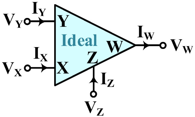
The circuit symbol of an ideal CFOA.
2.1. Proposed Voltage-Mode UAF Configuration
The proposed voltage-mode UAF configuration is shown in Figure 2, which consists of three CFOAs, two grounded capacitors, and six resistors. In Figure 2, the input signals Vi1, Vi2, and Vi3 are connected to the high input terminal of each Y terminal of the three CFOAs. The output voltages Vo1, Vo2, and Vo3 are connected to the low output terminal of each W terminal of the three CFOAs. High-input and low-output impedances can be used for cascaded voltage-mode operation without requiring any voltage buffers. Routine analysis of the voltage-mode UAF in Figure 2 gives the following four output voltages:
| (1) |
| (2) |
| (3) |
| (4) |
Figure 2.

The proposed voltage-mode UAF configuration.
According to (1)–(4), when the two input voltages of Vi1 and Vi2 are grounded, and Vi3 is provided as the input signal of Vin, four different filtering functions can be realized simultaneously.
| (5) |
| (6) |
| (7) |
| (8) |
From (5) to (8), the filter parameters bandwidth (BW), ωo, Q, passband gain a1 and a2, and BR frequency ωz are given by
| (9) |
| (10) |
| (11) |
Based on (5) to (7), an inverting band-pass (IBP) filtering function with R1/R2 passband gain is obtained at Vo1, a non-inverting LP (NLP) filtering function with unity passband gain is obtained at Vo2, and a non-inverting HP (NHP) filtering function with R1/R2 passband gain is obtained at Vo3. According to (8), the following three BR filtering functions are obtained.
-
(a)
If R1 = R2 and R5 = R6, the regular BR filtering function with 1/2 passband gain can be realized in (12).
| (12) |
-
(b)
If R5 < R6 and ωz > ωo, the LPN filtering function can be obtained in (8).
-
(c)
If R5 > R6 and ωz < ωo, the HPN filtering function can also be obtained in (8).
By connecting three input signals of Vi1, Vi2, and Vi3 into one input signal and selecting the matching element condition of R1 = R2 and C1R3 = 2C2R4, the voltage-mode UAF of Vo3 performs the following non-inverting AP (NAP) filtering function.
| (13) |
According to (9), the voltage-mode UAF parameters BW, ωo, and Q can be controlled orthogonally by R1 = R3 = Ra. In this particular case, (9) becomes
| (14) |
Equation (14) expresses that Ra independently controls the parameters BW and Q without affecting the parameter ωo. When R3 = R4 = Rb, the parameters ωo and Q in (9) become
| (15) |
Equation (15) expresses that Rb independently controls the parameter ωo without affecting the parameter Q. Equations (14) and (15) show that the voltage-mode UAF parameters Q and ωo are independently controlled by Ra and Rb, respectively.
2.2. Effects of CFOA Non-Idealities on Voltage-Mode UAF Characteristics
Assuming the non-ideal CFOA terminal characteristics as VX = βVY, VW = γVZ, and IX = αIZ, where β = 1 − εβv, γ = 1 − εγv and α = 1 − εαi. Here, εβv (|εβv| << 1) and εγv (|εγv| << 1) denote the voltage tracking errors of CFOA, and εαi (|εαi| << 1) represent the current tracking error of non-ideal CFOA [31]. Considering the non-ideal CFOA terminal characteristics in Figure 2, the analysis of voltage-mode UAF yields the denominator of the non-ideal voltage transfer function as follows.
| (16) |
The voltage-mode UAF parameters ωo and Q, in the case of non-ideal CFOA terminal characteristics, are
| (17) |
According to the definition of [43], the active and passive sensitivity parameters ωo and Q of voltage-mode UAF are calculated as follows.
| (18) |
| (19) |
| (20) |
| (21) |
From the results, the voltage-mode UAF exhibits low active and passive sensitivities.
If Vi1 and Vi2 are grounded, and only Vi3 is provided as the input signal of Vin, the four different filtering functions for non-ideal voltage and current gains become
| (22) |
| (23) |
| (24) |
| (25) |
The CFOA terminal characteristics generally have various parasitic impedances [43]. The parasitic impedances of these non-ideal CFOAs can affect the performance of the proposed voltage-mode UAF. Figure 3 illustrates the non-ideal CFOA model for analyzing the parasitic impedances and their effect on the voltage-mode UAF configuration. Using the CFOA non-ideal model, the parasitic impedance effect of the proposed voltage-mode UAF is analyzed, as shown in Figure 4. Reanalyzing the voltage-mode UAF in Figure 4, the following non-ideal four output node voltages are obtained:
| (26) |
| (27) |
| (28) |
| (29) |
Figure 3.

The effect of parasitic resistances and capacitances on ideal CFOA.
Figure 4.

The effect of CFOA parasitic resistances and capacitances on the voltage-mode UAF configuration.
Equations (26)–(29) show that several parasitic resistances of RX1, RX2, RX3, RZ1, RZ2, and RZ3 and three parasitic capacitances of CZ1, CZ2, and CZ3 will affect the voltage-mode UAF. In Figure 4, the proposed voltage-mode UAF has the attractive advantage that capacitors C1 and C2 are grounded, and resistors R2, R3, and R4 are connected to the X-terminal of the CFOA, respectively. The main advantage of the proposed voltage-mode UAF topology is that the two parasitic capacitance effects of CZ1 and CZ2 can be absorbed by the two grounded capacitors of C1 and C2, and the three parasitic resistances of RX1, RX2, and RX3 can also be absorbed by three series resistors of R3, R4, and R2, respectively. It is worth noting that the parasitic capacitance CZ3 and the parasitic resistances RZ1, RZ2, and RZ3 affect the operating frequency range of voltage-mode UAF. If the conditions of s(C1 + CZ1) >> 1/RZ1, s(C2 + CZ2) >> 1/RZ2, and sCZ3(R1//RZ3) << 1 are satisfied, the influence of the parasitic resistances and capacitances on voltage-mode UAF topology can be reduced. Therefore, the valid operating frequency range of the voltage-mode UAF needs to be considered as follows.
| (30) |
According to (30), the non-ideal three output node voltages of (26) to (28) are simplified as
| (31) |
| (32) |
| (33) |
In this case, the three non-ideal voltage transfer functions, the denominator Dn(s), and the non-ideal filter parameters of ωon and Qn were obtained as
| (34) |
| (35) |
| (36) |
| (37) |
| (38) |
| (39) |
If Vi1 and Vi2 are grounded, and only Vi3 is provided as the input signal of Vin, the four different filtering functions for non-ideal voltage outputs become
| (40) |
| (41) |
| (42) |
| (43) |
As shown in (30), the voltage-mode UAF must operate within the effective operating frequency range to minimize the effects of the non-ideal CFOA parasitic resistances and capacitances.
3. Simulation and Experimental Results
The proposed voltage-mode UAF efficiency and flexibility were demonstrated using commercially available off-the-shelf AD844AN ICs and on-chip design measurements to validate the theoretical analysis. The AD844-based voltage-mode UAF has a supply voltage of 12 V (±6 V) and a power consumption of 168 mW. The on-chip CMOS CFOA-based VM-UAF has a supply voltage of 1.8 V (±0.9 V) and a power consumption of 3.6 mW. The performance of the AD844-based voltage-mode UAF and on-chip CMOS CFOA-based voltage-mode UAF was evaluated using the OrCAD PSpice software and the Synopsys HSpice simulation design environment using TSMC 180 nm 1P6M CMOS technology, respectively. Simulations were performed using the built-in library of AD844/AD model parameters of OrCAD PSpice software, and OrCAD PSpice software features sensitivity/Monte Carlo analysis capabilities. The experimental setups of AD844-based voltage-mode UAF and on-chip CMOS CFOA-based voltage-mode UAF are shown in Figure 5 and Figure 6, respectively. Frequency domain simulations evaluate the AD844-based voltage-mode UAF and on-chip CMOS CFOA-based voltage-mode UAF. Measurements on an AD844-based voltage-mode UAF and a CFOA-based voltage-mode UAF chip validate and confirm the theoretical analysis.
Figure 5.

AD844-based voltage-mode UAF experimental setup platform.
Figure 6.

On-chip CMOS CFOA-based voltage-mode UAF experimental setup platform.
3.1. The AD844-Based Voltage-Mode UAF Simulation and Measurement Results
The passive components of the AD844-based voltage-mode UAF are selected as C1 = C2 = 100 pF and Ri = 10 kΩ (i = 1 to 6) with a resonance frequency of fo = 159.15 kHz. Regarding the AD844 datasheet [44], the X terminal parasitic resistance of AD844 is RX = 50 Ω. The Z terminal parasitic resistance and parasitic capacitance of AD844 are RZ = 3 MΩ and CZ = 4.5 pF, respectively. According to (30), the effective operating frequency range of the AD844-based voltage-mode UAF is 1.74 kHz to 885.37 kHz. Figure 7 shows the simulated frequency spectrum of the IBP filtering response at Vo1. As shown in Figure 7, the total harmonic distortion (THD) is calculated as 0.6% for a sinusoidal input voltage of 2.4 Vpp. Figure 8 shows the measured frequency spectrum of the IBP filtering response at Vo1. As shown in Figure 8, the THD is calculated as 1.68% for a sinusoidal input voltage of 5.2 Vpp, and the measured spurious-free dynamic range is 37.62 dBc. The gain and phase of AD844-based VM-UAF in the frequency domain simulations are shown in Figure 9, Figure 10, Figure 11 and Figure 12. Figure 13, Figure 14, Figure 15 and Figure 16 also show the measurements for the AD844-based voltage-mode UAF. The experimental and simulation results of the AD844-based voltage-mode UAF relative to the theoretical analysis are shown in Figure 17, Figure 18, Figure 19 and Figure 20. It can be seen that the experimental and simulation results of the AD844-based voltage-mode UAF are close to the theoretical predictions.
Figure 7.

The simulated frequency spectrum for the AD844-based voltage-mode UAF at Vo1 IBP filter.
Figure 8.

The measured frequency spectrum for the AD844-based voltage-mode UAF at Vo1 IBP filter, where # is the reference symbol.
Figure 9.

Simulation results for the AD844-based voltage-mode UAF at Vo1 IBP filter.
Figure 10.

Simulation results for the AD844-based voltage-mode UAF at Vo2 NLP filter.
Figure 11.

Simulation results for the AD844-based voltage-mode UAF at Vo3 NHP filter.
Figure 12.

Simulation results for the AD844-based voltage-mode UAF at Vo4 BR filter.
Figure 13.

Gain (top) and phase (bottom) measurement results for the AD844-based voltage-mode UAF at Vo1 IBP filter.
Figure 14.

Gain (top) and phase (bottom) measurement results for the AD844-based voltage-mode UAF at Vo2 NLP filter.
Figure 15.

Gain (top) and phase (bottom) measurement results for the AD844-based voltage-mode UAF at Vo3 NHP filter.
Figure 16.

Gain (top) and phase (bottom) measurement results for the AD844-based voltage-mode UAF at Vo4 BR filter.
Figure 17.

Ideal, simulated, and measured results for the AD844-based voltage-mode UAF at Vo1 IBP filter.
Figure 18.

Ideal, simulated, and measured results for the AD844-based voltage-mode UAF at Vo2 NLP filter.
Figure 19.

Ideal, simulated, and measured results for the AD844-based voltage-mode UAF at Vo3 NHP filter.
Figure 20.

Ideal, simulated, and measured results for the AD844-based voltage-mode UAF at Vo4 BR filter.
According to (14), R1 = R3 = Ra can independently control the Q value in the AD844-based voltage-mode UAF without affecting the parameter ωo. Thus, with fixed C1 = C2 = 300 pF and R2 = R4 = 4 kΩ, the required Ra values are 3.2 kΩ, 5.44 kΩ, 7.68 kΩ, and 10 kΩ for selected Q values of 0.8, 1.36, 1.92, and 2.5, respectively. Figure 21, Figure 22 and Figure 23 show the behavior of the AD844-based VM-UAF quality factor independently controlled by Ra when Vi3 = Vin and Vi1 = Vi2 = 0. According to (15), R3 = R4 = Rb can independently control the resonance frequency value in the AD844-based voltage-mode UAF without affecting the parameter Q. Thus, with fixed C1 = C2 = 100 pF and R1 = R2 = 10 kΩ, the required Rb values are 50 kΩ, 24 kΩ, 12 kΩ, and 6 kΩ for selected resonant frequency values of 31.83 kHz, 66.31 kHz, 132.62 kHz, and 265.26 kΩ, respectively. Figure 24, Figure 25 and Figure 26 show the behavior of the AD844-based voltage-mode UAF resonant frequency fo independently controlled by Rb when Vi3 = Vin and Vi1 = Vi2 = 0. As shown in Figure 23 and Figure 26, simulations and measurements confirm the theoretical analysis according to (14) and (15).
Figure 21.

The simulated quality factor for the AD844-based voltage-mode UAF.
Figure 22.

The measured quality factor for the AD844-based voltage-mode UAF.
Figure 23.

Ideal, simulated, and measured results for independent quality factor control.
Figure 24.

The simulated resonant frequency for the AD844-based voltage-mode UAF without affecting the parameter Q.
Figure 25.

The measured resonant frequency for the AD844-based voltage-mode UAF without affecting the parameter Q.
Figure 26.

Ideal, simulated, and measured results for independent resonant frequency control without affecting the parameter Q.
3.2. The On-Chip CMOS VM-UAF Simulation and Measurement Results
Passive components of the on-chip CMOS CFOA-based voltage-mode UAF are designed as C1 = C2 = 15 pF and Ri = 20 kΩ (i = 1 to 6) with a resonance frequency of fo = 530.5 kHz. Figure 27 shows the overall layout of the CFOA-based voltage-mode UAF and its chip micrograph with two CFOA-based voltage-mode UAFs. The CMOS implementation of CFOA is shown in Figure 28 [40]. In Figure 28, the length (L) and width (W) of transistors M1 to M16 are 0.4 μm and 75 μm, the L and W of transistors M17 to M20 are 0.8 μm and 13 μm, and the L and W of transistors M21 to M28 are 0.4 μm and 26 μm. Figure 29 shows the simulated frequency spectrum of the IBP filtering response at Vo1. As shown in Figure 29, the THD is calculated as 0.25% for a sinusoidal input voltage of 0.4 Vpp. Figure 30 shows the measured frequency spectrum of the IBP filtering response at Vo1. As shown in Figure 30, the THD is calculated as 1% for a sinusoidal input voltage of 0.4 Vpp, and the measured spurious-free dynamic range is 43.55 dBc. Figure 31, Figure 32 and Figure 33 also show the measurements for the CFOA-based voltage-mode UAF chip. The experimental and simulation results of the CFOA-based voltage-mode UAF chip relative to the theoretical analysis are shown in Figure 34, Figure 35 and Figure 36, respectively.
Figure 27.

The overall layout of the CFOA-based voltage-mode UAF and its micrograph of a chip with two CFOA-based voltage-mode UAFs.
Figure 28.

The CMOS implementation of CFOA.
Figure 29.

The simulated frequency spectrum for the CFOA-based voltage-mode UAF chip at Vo1 IBP filter.
Figure 30.

The measured frequency spectrum for the CFOA-based voltage-mode UAF chip at Vo1 IBP filter, where # is the reference symbol.
Figure 31.

Gain (top) and phase (bottom) simulation results for the CFOA-based voltage-mode UAF chip at Vo1 IBP filter.
Figure 32.

Gain (top) and phase (bottom) simulation results for the CFOA-based voltage-mode UAF chip at Vo2 NLP filter.
Figure 33.

Gain (top) and phase (bottom) simulation results for the CFOA-based voltage-mode UAF chip at Vo3 NHP filter.
Figure 34.

Ideal, simulated, and measured results for the CFOA-based voltage-mode UAF chip at Vo1 IBP filter.
Figure 35.

Ideal, simulated, and measured results for the CFOA-based voltage-mode UAF chip at Vo2 NLP filter.
Figure 36.

Ideal, simulated, and measured results for the CFOA-based voltage-mode UAF chip at Vo3 NHP filter.
4. Conclusions
Three voltage-mode UAFs based on CFOA have been proposed in the technical literature, using four CFOAs, two grounded capacitors, five/six resistors, and one/two switches [43]. This study proposes a new voltage-mode UAF to improve the convenience and versatility of the recently introduced three voltage-mode UAF circuits [43]. The proposed voltage-mode UAF has three high-input and low-output impedances and can simultaneously realize LP, BP, HP, and BR filtering functions from the same configuration. Based on three CFOAs, the new voltage-mode UAF can be used in HP, LP, BP, BR, LPN, HPN, and AP without switches, providing the versatility and utility that active filter designers have expected. The proposed voltage-mode UAF has the following advantages: (1) configuration requires no switches and uses only three CFOAs, two grounded capacitors, and six resistors, (2) using two grounded capacitors is suitable for IC implementation, (3) the voltage-mode second-order LP, BP, HP, BR, LPN, HPN, and AP filtering functions are implemented from the same circuit configuration, (4) three high-input and low-output impedances are available for voltage-mode operation without needing voltage buffers, (5) the voltage-mode second-order LP, BP, HP, and BR second-order filtering functions are realized simultaneously without component matching conditions, (6) there is no series capacitor at the X-terminal of the CFOA, (7) the AP filtering function can be realized without voltage inverters or switches, (8) the ωo and Q have independent controllability under certain circumstances, (9) the voltage-mode UAF has low active and passive sensitivity performance, and (10) The voltage-mode UAF circuit is implemented into a single CFOA-based chip. The CFOA-based voltage-mode UAF chip has lower power consumption and higher integration than the AD844-based filter. Experimental results from the commercially available off-the-shelf AD844 ICs and on-chip design measurements validate the theoretical analysis.
Author Contributions
Methodology and writing—original draft preparation H.-P.C.; formal analysis and investigation, H.-P.C., I.-C.W. and S.-F.W.; Software, L.-Y.C. and C.-Y.W.; Validation, H.-P.C., I.-C.W., L.-Y.C., C.-Y.W., and S.-F.W. All authors have read and agreed to the published version of the manuscript.
Institutional Review Board Statement
Not applicable.
Informed Consent Statement
Not applicable.
Data Availability Statement
Not applicable.
Conflicts of Interest
The authors declare no conflict of interest.
Funding Statement
This research received no external funding.
Footnotes
Disclaimer/Publisher’s Note: The statements, opinions and data contained in all publications are solely those of the individual author(s) and contributor(s) and not of MDPI and/or the editor(s). MDPI and/or the editor(s) disclaim responsibility for any injury to people or property resulting from any ideas, methods, instructions or products referred to in the content.
References
- 1.Kumngern M., Aupithak N., Khateb F., Kulej T. 0.5 V Fifth-order butterworth low-pass filter using multiple-input OTA for ECG applications. Sensors. 2020;20:7343. doi: 10.3390/s20247343. [DOI] [PMC free article] [PubMed] [Google Scholar]
- 2.Tangsangiumvisai N., Chambers J.A., Constantinides A.G. Higher-order time-varying allpass filters for signal decorrelation in stereophonic acoustic echo cancellation. Electron. Lett. 1999;35:88–90. doi: 10.1049/el:19990036. [DOI] [Google Scholar]
- 3.Chiu W.Y., Horng J.W. High-input and low-output impedance voltage-mode universal biquadratic filter using DDCCs. IEEE Trans. Circuits Syst. II Exp. Briefs. 2007;54:649–652. doi: 10.1109/TCSII.2007.899460. [DOI] [Google Scholar]
- 4.Prommee P., Karawanich K., Khateb F., Kulej T. Voltage-mode elliptic band-pass filter based on multiple-input transconductor. IEEE Access. 2021;9:32582–32590. doi: 10.1109/ACCESS.2021.3060939. [DOI] [Google Scholar]
- 5.Sotner R., Jerabek J., Polak L., Theumer R., Langhammer L. Electronic tunability and cancellation of serial losses in wire coils. Sensors. 2022;22:7373. doi: 10.3390/s22197373. [DOI] [PMC free article] [PubMed] [Google Scholar]
- 6.Zhao Z., Tong H., Deng Y., Xu W., Zhang Y., Ye H. Single-lead fetal ECG extraction based on a parallel marginalized particle filter. Sensors. 2017;17:1456. doi: 10.3390/s17061456. [DOI] [PMC free article] [PubMed] [Google Scholar]
- 7.Márquez A., Pérez-Bailón J., Calvo B., Medrano N., Martínez P.A. A CMOS self-contained quadrature signal generator for SoC impedance spectroscopy. Sensors. 2018;18:1382. doi: 10.3390/s18051382. [DOI] [PMC free article] [PubMed] [Google Scholar]
- 8.Yuce E. Voltage-mode multifunction filters employing a single DVCC and grounded capacitors. IEEE Trans. Instrum. Meas. 2009;58:2216–2221. doi: 10.1109/TIM.2009.2013671. [DOI] [Google Scholar]
- 9.Lee C.N. Independently tunable plus-type DDCC-based voltage-mode universal biquad filter with MISO and SIMO types. Microelectron J. 2017;67:71–81. doi: 10.1016/j.mejo.2017.07.006. [DOI] [Google Scholar]
- 10.Roongmuanpha N., Likhitkitwoerakul N., Fukuhara M., Tangsrirat W. Single VDGA-based mixed-mode electronically tunable first-order universal filter. Sensors. 2023;23:2759. doi: 10.3390/s23052759. [DOI] [PMC free article] [PubMed] [Google Scholar]
- 11.Akbari M., Hussein S.M., Hashim Y., Tang K.T. An adjustable dual-output current mode MOSFET-only filter. IEEE Trans. Circuits Syst. II Exp. Briefs. 2021;68:1817–1821. doi: 10.1109/TCSII.2020.3044464. [DOI] [Google Scholar]
- 12.Alpaslan H., Yuce E. DVCC+ based multifunction and universal filters with the high input impedance features. Analog Integr. Circuits Signal Process. 2020;103:325–335. doi: 10.1007/s10470-020-01643-8. [DOI] [Google Scholar]
- 13.Lee C.N. Fully Cascadable mixed-mode universal filter biquad using DDCCs and grounded passive components. J. Circuits Syst. Comput. 2011;20:607–620. doi: 10.1142/S0218126611007499. [DOI] [Google Scholar]
- 14.Kumngern M., Khateb F., Kulej T., Psychalions C. Multiple-input universal filter and quadrature oscillator using multiple-input operational transconductance amplifiers. IEEE Access. 2021;9:56253–56263. doi: 10.1109/ACCESS.2021.3071829. [DOI] [Google Scholar]
- 15.Khateb F., Kumngern M., Kulej T., Biolek D. 0.5 V differential difference transconductance amplifier and its application in voltage-mode universal filter. IEEE Access. 2022;10:43209–43220. doi: 10.1109/ACCESS.2022.3167700. [DOI] [PMC free article] [PubMed] [Google Scholar]
- 16.Fabre A., Saaid O., Barthelemy H. On the frequency limitations of the circuits based on second generation current conveyors. Analog Integr. Circuits Signal Process. 1995;7:113–129. doi: 10.1007/BF01239166. [DOI] [Google Scholar]
- 17.Supavarasuwat P., Kumngern M., Sangyaem S., Jaikla W., Khateb F. Cascadable independently and electronically tunable voltage-mode universal filter with grounded passive components. AEU Int. J. Electron. Commun. 2018;84:290–299. doi: 10.1016/j.aeue.2017.12.002. [DOI] [Google Scholar]
- 18.Wai M.P.P., Suwanjan P., Jaikla W., Chaichana A. Electronically and orthogonally tunable SITO voltage-mode multifunction biquad filter using LT1228s. Elektron. Ir Elektrotechnika. 2021;27:11–17. doi: 10.5755/j02.eie.28949. [DOI] [Google Scholar]
- 19.Schmid H. Why “current mode” does not guarantee good performance. Analog Integr. Circuits Signal Process. 2003;35:79–90. doi: 10.1023/A:1023477605076. [DOI] [Google Scholar]
- 20.Liu S.I., Wu D.S. New current-feedback amplifier-based universal biquadratic filter. IEEE Trans. Instrum. Meas. 1995;44:915–917. [Google Scholar]
- 21.Soliman A.M. A new filter configuration using current feedback op-amp. Microelectron. J. 1998;29:409–419. doi: 10.1016/S0026-2692(97)00025-6. [DOI] [Google Scholar]
- 22.Bhaskar D.R. Realisation of second-order sinusoidal oscillator/filters with non-interacting controls using CFAs. Frequenz. 2003;57:12–14. doi: 10.1515/FREQ.2003.57.1-2.12. [DOI] [Google Scholar]
- 23.Shan N.A., Rather M.F., Iqbal S.Z. CFA-based three input and two outputs voltage-mode universal filter. Indian J. Pure Appl. Phy. 2005;43:636–639. [Google Scholar]
- 24.Nikoloudis S., Psychalinos C. Multiple input single output universal biquad filter with current feedback operational amplifiers. Circuits Syst. Signal Process. 2010;29:1167–1180. doi: 10.1007/s00034-010-9194-4. [DOI] [Google Scholar]
- 25.Topaloglu S., Sagbas M., Anday F. Three-input single-output second-order filters using current-feedback amplifiers. AEU Int. J. Electron. Commun. 2012;66:683–686. doi: 10.1016/j.aeue.2011.12.009. [DOI] [Google Scholar]
- 26.Verma R., Pandey N., Pandey R. CFOA based low pass and high pass fractional step filter realizations. AEU Int. J. Electron. Commun. 2019;99:61–76. doi: 10.1016/j.aeue.2018.11.032. [DOI] [Google Scholar]
- 27.Chang C.M., Hwang C.S., Tu S.H. Voltage-mode notch, lowpass and bandpass filter using current-feedback amplifiers. Electron. Lett. 1994;30:2022–2023. doi: 10.1049/el:19941416. [DOI] [Google Scholar]
- 28.Soliman A.M. Applications of the current feedback operational amplifiers. Analog Integr. Circuits Signal Process. 1996;11:265–302. doi: 10.1007/BF00240490. [DOI] [Google Scholar]
- 29.Horng J.W., Lee M.H. High input impedance voltage-mode lowpass, bandpass and highpass filter using current-feedback amplifiers. Electron. Lett. 1997;33:947–948. doi: 10.1049/el:19970618. [DOI] [Google Scholar]
- 30.Senani R. Realization of a class of analog signal processing/signal generation circuits: Novel configurations using current feedback op-amps. Frequenz. 1998;52:196–206. doi: 10.1515/FREQ.1998.52.9-10.196. [DOI] [Google Scholar]
- 31.Abuelma’atti M.T., Al-zaher H.A. New universal filter with one input and five outputs using current-feedback amplifiers. Analog Integr. Circuits Signal Process. 1998;16:239–244. doi: 10.1023/A:1008266223999. [DOI] [Google Scholar]
- 32.Singh A.K., Senani R. CFOA-based state-variable biquad and its high-frequency compensation. IEICE Electron. Express. 2005;2:232–238. doi: 10.1587/elex.2.232. [DOI] [Google Scholar]
- 33.Shah N.A., Iqbal S.Z., Rather M.F. Versatile voltage-mode CFA-based universal filter. AEU Int. J. Electron. Commun. 2005;59:192–194. doi: 10.1016/j.aeue.2004.11.037. [DOI] [Google Scholar]
- 34.Shan N.A., Malik M.A. High input impedance voltage-mode lowpass, bandpass, highpass and notch filter using current feedback amplifiers. Indian J. Eng. Mater. Sci. 2005;12:278–280. [Google Scholar]
- 35.Shan N.A., Malik M.A. New high input impedance voltage-mode lowpass, bandpass and highpass filter using current feedback amplifiers. J. Circuits Sys. Comp. 2005;14:1037–1043. [Google Scholar]
- 36.Singh V.K., Singh A.K., Bhaskar D.R., Senani R. New universal biquads employing CFOAs. IEEE Trans. Circuits Syst. II Exp. Briefs. 2006;53:1299–1303. doi: 10.1109/TCSII.2006.882345. [DOI] [Google Scholar]
- 37.Wang S.F., Chen H.P., Ku Y., Chen P.Y. A CFOA-based voltage-mode multifunction biquadratic filter and a quadrature oscillator using the CFOA-based biquadratic filter. Appl. Sci. 2019;9:2304. doi: 10.3390/app9112304. [DOI] [Google Scholar]
- 38.Wang S.F., Chen H.P., Ku Y., Zhong M.X. Voltage-mode multifunction biquad filter and its application as fully-uncoupled quadrature oscillator based on current-feedback operational amplifiers. Sensors. 2020;20:6681. doi: 10.3390/s20226681. [DOI] [PMC free article] [PubMed] [Google Scholar]
- 39.Wang S.F., Chen H.P., Ku Y., Li Y.F. High-input impedance voltage-mode multifunction filter. Appl. Sci. 2021;11:387. doi: 10.3390/app11010387. [DOI] [Google Scholar]
- 40.Wang S.F., Chen H.P., Ku Y., Zhong M.X. Analytical synthesis of high-pass, band-pass and low-pass biquadratic filters and its quadrature oscillator application using current-feedback operational amplifiers. IEEE Access. 2021;9:13330–13343. doi: 10.1109/ACCESS.2021.3050751. [DOI] [Google Scholar]
- 41.Chen H.P., Wang S.F., Ku Y., Yeh A.C., Chen Y.H. Design of second-order multifunction filter IC based on current feedback amplifiers with independent voltage gain control. IEEE Access. 2022;10:63301–63313. doi: 10.1109/ACCESS.2022.3183226. [DOI] [Google Scholar]
- 42.Chen H.P., Wang S.F., Ku Y., Yi Y.C., Chen Y.H. Experimental verification of on-chip biquadratic filter and oscillator. IEEE Sens. J. 2023;23:3736–3746. doi: 10.1109/JSEN.2023.3234250. [DOI] [Google Scholar]
- 43.Bhaskar D.R., Raj A., Senani R. Three new CFOA-based SIMO-type universal active filter configurations with unrivalled features. AEU Int. J. Electron. Commun. 2022;153:154285. doi: 10.1016/j.aeue.2022.154285. [DOI] [Google Scholar]
- 44.AD844: 60 MHz, 2000 V/μs, Monolithic Op-amp with Quad Low Noise Data Sheet (Rev. G). May 2017. [(accessed on 1 December 2020)]. Available online: www.linear.com.
Associated Data
This section collects any data citations, data availability statements, or supplementary materials included in this article.
Data Availability Statement
Not applicable.