

Abstract
We report the implementation of a color-capable on-chip lensless microscope system, termed color optofluidic microscope (color OFM), and demonstrate imaging of double stained Caenorhabditis elegans with lacZ gene expression at a light intensity about 10 mW/cm2.
In the field of modern clinical diagnostics and biological science research, the development of microscopes that are autonomous, compact, low-cost and high-resolution can potentially improve existing microscopy applications and engender new microscope usage. The lensless and fully on-chip microscope systems, termed the optofluidic microscopes (OFM), reported recently can potentially fill this role.1,2 In brief, the OFM method utilizes microfluidic flow to transport samples across array(s) of small apertures (1 micron or smaller) on a metal-coated CMOS imaging sensor that is illuminated with light. The passage of a sample interrupts light transmission through the apertures, and the time-varying transmission associated with each aperture effectively represents a line trace across the sample. By appropriately compositing these line traces from these apertures, we can then generate a high-resolution image of the sample at a resolution comparable to the aperture size. The diagonal arrangement of the aperture array across the channel floor allows the aperture arrays to fully scan a sample flowing in the channel. Due to this design, sensor pixel size has no impact on the OFM’s resolution.1 In addition, the absence of lenses and other bulk optical elements in the OFM design is particularly advantageous as it allows us to implement highly compact chip-scale microscope systems that are mass-producible in a semiconductor foundry. Finally, as the OFM can directly process samples in fluid media, this method eliminates the need to prepare fluid samples onto a glass slide for standard microscopy examination.
The basic OFM design can be altered to provide additional imaging capability. For example, we recently presented a proof-of-concept for phase imaging in the OFM format based on the use of tightly clustered apertures.3
In this paper, we present an OFM system that is capable of performing color imaging. This system uses a color CMOS sensor chip in place of a monochromatic CMOS sensor chip in the standard OFM, and employs an aperture array arrangement that accommodates the Bayer color pixel arrangement on such sensors.
In the next few paragraphs, we will describe the specifications and operating principle of our color OFM prototype. Next, we will report on the calibration experiments for our prototype and demonstrate that it is capable of determining the concentration of a dye, Trypan Blue, under varying illumination intensity. Finally, we will show color OFM images of the microscopic nematode Caenorhabditis elegans (C. elegans) expressing β-galactosidase with a blue LacZ stain and Ponceau, a nonspecific red stain.
The color OFM prototype was fabricated on a color CMOS sensor substrate; the sensor (Aptina, MT9T001P12STC) consists of 2048 × 1536 pixels of size 3.2 micron. Each of these pixels is coated with one of three different chromatic filters that nominally transmit the red (R), green (G) or blue (B) region of the optical spectrum. The color pixels are arranged in a 2 × 2 Bayer pattern consisting of two diagonal green pixels, one red pixel and one blue pixel as shown in Fig. 1(b).
Fig. 1.
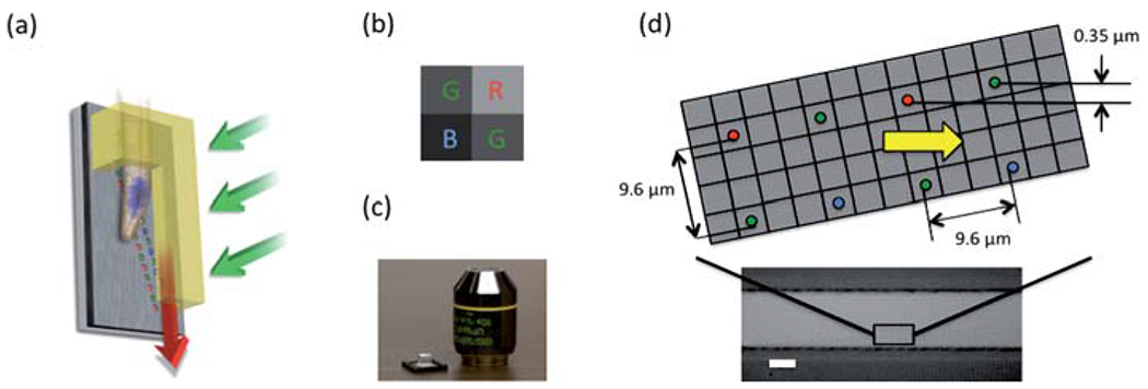
(a) The schematic plot of gravity driven color OFM. (b) The Bayer pattern for the color filter mask of the CMOS sensor. (c) The color OFM device comparing its size with a 10× microscope objective. (d) The schematic plot for the aperture array and the microscope image of an aligned PDMS channel on top of the aperture array. The scale bar is 20 microns.
We spin-coated a polymethyl methacrylate (PMMA) layer of 300 nm in thickness to planarize the sensor’s surface. We next used a metal evaporator with thermal source (CHA Industries, Mark 40) to deposit a 300 nm thick aluminium layer on top of the PMMA layer. (At these layer thicknesses, the outlines of individual pixels were still discernible under SEM imaging and the surface was sufficiently flat to allow subsequent bonding of a PDMS block containing a microfluidic channel onto the chip.) We then used a focused ion beam machine (FEI Company, Nova200) to mill two arrays of 140 apertures on the aluminium layer. Then another 200 nm PMMA layer was spin coated on the aluminium layer to protect the aperture. The diameter of the aperture was 0.7 μm. The apertures were spaced 9.6 μm apart (equal to 3-pixel width). The two arrays were also spaced 9.6 μm apart. The relatively wide spacing choice was made to minimize crosstalk effects from neighboring pixels. We ensured that the apertures were each milled directly above a single sensor pixel by exacting good control over the milling process. The apertures of the first and second array were patterned over the color pixels in repeating sequence of -RG- and -GB- respectively. Finally, we attached a polydimethylsiloxane (PDMS) block containing a soft-lithography patterned microfluidic channel onto the sensor with a mask aligner (Karl Suss, MJB3). The channel was 40 μm in width and 20 μm in height. The channel was set at an angle of 0.05 radian to the aperture array. This ensured that apertures associated with the same color overlapped each other by 0.7 μm across the width of the channel (see Fig. 1(d)). The system was uniformly illuminated with light (~10 mW/cm2) from a halogen lamp.
We programmed the sensor to specifically read signals from the two lines of pixels directly below the aperture arrays. The readout rate was 1.3 kHz/s. The time-varying transmission change measured through each aperture represents a line scan of a sample passing through the microfluidic channel. By stacking the line scans from the apertures together, we can then generate an image of the sample. Based on the aperture size, we have previously established that such a system has a resolution of 0.8 μm at its plane of highest acuity (bottom of the channel).4
The image forming mechanism of OFM is different from that of the conventional microscope. Instead of collecting the light from a scattering spot within a certain collection angle, OFM uses small apertures to locally sample the light projection from the specimen. Thus the light collection efficiency through the aperture at different wavelength needs to be quantified. The spectral response of the device is measured by illuminating the device with light of different wavelength selected by a mono-chronometer. We recorded the spectral response range from 400–600 nm in 20 nm step increments. Fig. 2 shows the spectral response for the red, green, and blue pixels from the OFM device and compares that with an unprocessed color CMOS sensor. The results show that the blue and green pixels’ spectral responses were slightly impacted by the presence of the apertures while the red pixel showed some deviations. The impact is sufficiently moderate and positively indicates that our fabrication procedures did not significantly degrade the chromatic filters on the pixels. This set of data is helpful in aiding us renormalize the OFM measurements.
Fig. 2.
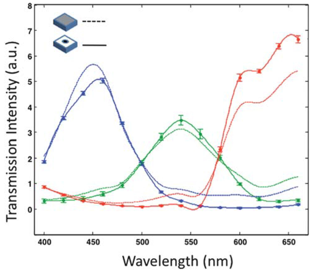
The aperture effect on spectral response of the sensor: the solid lines represent the measured transmission data from a color OFM device; the dash lines are the response from a CMOS sensor without any fabrication process. All the transmission data are normalized at 400 nm.
One of the advantages of color imaging is that the multi-spectral information can be used to quantify the relative concentration of the dye used in stained samples. For example, the optical signal detected by a blue pixel can be mathematically expressed as:
| (1) |
where is the optical signal detectable in the absence of a sample, is the dye’s absorption cross-section in the blue spectral region; n is the concentration of the dye; and l is the optical path length. We can write similar expressions for the red and green pixels. If the dye’s absorption cross-section spectral variation is known, we can therefore determine the dye concentration by making four measurements: , , and . The dye concentration can then be calculated from:
| (2) |
we can see the linear relationship between and the slope is independent of the illumination intensity, and . In this example, we chose the red and blue pixels as the target pixel pair. We can alternately pick any paired combination of the three color pixels. We should ideally pick the color pixel associated with the largest dye absorption cross-section and the color pixel associated with the smallest dye absorption cross-section to maximize sensitivity.
To verify this capability, we flowed a blue dye, Trypan Blue, at varying concentration through a color OFM system. The microfluidic channel was 28 μm in height. The illumination intensity was 4 mW/cm2. We varied the Trypan Blue concentration from 0 to 1.2 mM in 0.2 mM increments. The and measurements were acquired with pixels directly underneath the channel while the and measurements were acquired from pixels that were not covered by the channel. The result shown in Fig. 3 verifies that the measured ratio is a linear function of the dye concentration. To verify that this ratio is independent of the illumination intensity, we repeated the experiment at a higher illumination intensity of 6 mW/cm2 by increasing the power of the halogen lamp. Fig. 3 shows that the measured ratio overlapped with that of the original experiment.
Fig. 3.
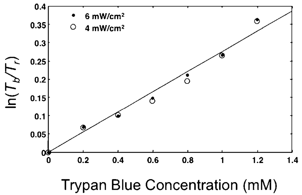
Dye concentration measured by the logarithm of relative intensity of two different colors. The illumination light passes through Trypan Blue solutions with two intensities of 6mW/cm2 and 4mW/cm2.
Next, we demonstrated our prototype by imaging C. elegans stained for Lac Z expression. The LacZ (β-galactosidase) gene is frequently used as a reporter in some bacterial-based selection techniques.5 The location where LacZ is expressed can be easily located with a LacZ stain containing the artificial substrate X-gal, which turns blue when it is cleaved by β-galactosidase.
The C. elegans (pPD82.51) strain used contains a myo-2::lacZ fusion, which when expressed, stains the pharyngeal muscles of the worm’s head blue after treatment with the X-gal, purchased from Caenorhabditis Genetics Center. The worms were fixed at their early larval stage L-1. We used the Lac Z Tissue Staining Kit (rep-lz-t, InvivoGen) for staining, and followed the protocol. We additionally stained the worms with Ponceau-S, a stain commonly used to visualize proteins on Western blots, as a method to obtain a second color, red, simultaneously on one worm. The stained worms were resuspended in 1× PBS with a concentration of about 10 worms/μL.
By operating the color OFM on an inclined plane, we were able to induce the C. elegans worms to flow through the microfluidic channel via gravitational pull. The transportation velocity ranged from 500 μm/s to 1000 μm/s. As in our previous experiments, we used the same halogen lamp as our light source. At this speed range and sensor readout speed, we can sample the worms in less than 0.5 μm intervals along the flow channel direction. This ensured adequate sampling and ensured that the image resolution is limited by the aperture size.1
As both aperture arrays contained green pixels, we can constitute two green OFM images from the collected scans – one image for each set of green pixels. This redundancy was useful as it allowed us to (1) determine the flow speed of each worm, and (2) determine if the worms maintained their respective orientation and shape during the scan. The first task was accomplished by noting the time delay between when a worm passed the first and second green pixel array. By dividing the length separation between the arrays along the flow direction of the channel by this time delay, we can determine the flow speed. If a worm changed shape or orientation during the scan, we can expect the two green OFM images to look quite different. Therefore, the second task was accomplished by computing the cross-correlation between the two collected green images. We reject any image set that has a cross-correlation value lower than 0.5.1
Fig. 4 shows the color OFM images of a C. elegans. The LacZ stains the pharyngeal muscles of the worm blue, and Ponceau attached nonspecifically to proteins in the worm. The LacZ staining is clearly visible in the red and green OFM images, and is difficult to identify in the blue OFM images. This observation is consistent with the fact that the LacZ staining absorbs strongly in the red and green part of the spectrum and that it absorbs the blue part of the spectrum weakly. We balanced the ratio of the three color channels to ensure the background of the image has same value of the three components. The combined color image is comparable with a balanced brightfield image from a conventional microscope with a 10× objective using the same imaging sensor. The color OFM image can help us visualize the nonspecific Ponceau red staining in the middle and the tail part of the worm. Our prototype’s ability to image and distinguish color stains in samples represents a significant improvement over our previously reported OFM devices.
Fig. 4.
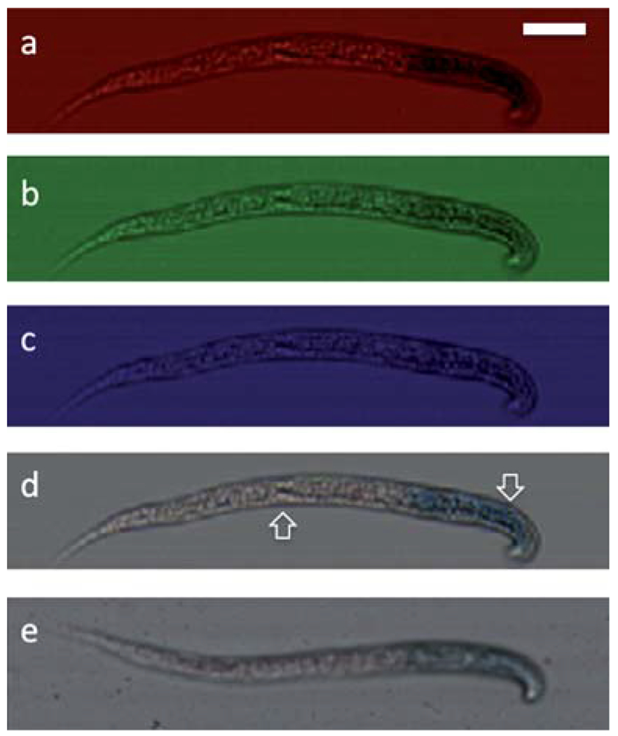
Construction of a color OFM image of C. elegans with LacZ expression. (a)–(c) From top to bottom are the images from red, green, blue pixels of a C. elegans with blue Xgal stain and Ponceau stain image, (d) the constructed color OFM image shows the nonspecific Ponceau stain (left arrow) and the LacZ staining of the pharyngeal muscles (right arrow), (e) the conventional 10× microscope image of the same sample. The scale bar is 20 microns.
As this color OFM design is microfluidic based, it can form part of a greater microfluidic analysis system in which sample prep and staining are all performed on chip. It is also possible to envision more sophisticated staining and imaging strategies that such a compact imaging system can be used optimally. For example, the color OFM can be used to automatically image samples that are sequentially stained with different dyes, in which imaging is performed after each staining step. Such a scheme is difficult to automate in a conventional laboratory, but is relatively simple to implement in a well-controlled microfluidic system.6
In summary, we reported the operating principle of the color OFM prototype, its calibration experiments, and its capability of determining the dye concentration with varying illumination intensity. We also demonstrated the imaging of a double stained C. elegans with lacZ gene expression with the color OFM device.
Acknowledgements
We would like to express our thanks to Dr Sri Rama Prasanna Pavani for the assistance of the experiments, Lap Man Lee and Dr Jigang Wu for constructive discussions. This work is supported by the Coulter Foundation and NIH R21EB008867.
References
- 1.Cui XQ, Lee LM, Heng X, Zhong WW, Sternberg PW, Psaltis D and Yang CH, Proc. Natl. Acad. Sci. U. S. A, 2008, 105, 10670–10675. [DOI] [PMC free article] [PubMed] [Google Scholar]
- 2.Heng X, Erickson D, Baugh LR, Yaqoob Z, Sternberg PW, Psaltis D and Yang CH, Lab Chip, 2006, 6, 1274–1276. [DOI] [PubMed] [Google Scholar]
- 3.Cui XQ, Lew M and Yang CH, Appl. Phys. Lett, 2008, 93,091113. [Google Scholar]
- 4.Heng X, Cui XQ, Knapp DW, Wu JG, Yaqoob Z, McDowell EJ, Psaltis D and Yang CH, Opt. Express, 2006, 14, 10410–10425. [DOI] [PubMed] [Google Scholar]
- 5.Joung JK, Ramm EI and Pabo CO, Proc. Natl. Acad. Sci. U. S. A, 2000, 97, 7382–7387. [DOI] [PMC free article] [PubMed] [Google Scholar]
- 6.Thorsen T, Maerkl SJ and Quake SR, Science, 2002, 298, 580–584. [DOI] [PubMed] [Google Scholar]