

Abstract
Electrophysiological recording and stimulation of neuron activities are important for us to understand the function and dysfunction of the nervous system. To record/stimulate neuron activities as voltage fluctuation extracellularly, microelectrode array (MEA) implants are a promising tool to provide high temporal and spatial resolution for neuroscience studies and medical treatments. The design configuration and recording capabilities of the MEAs have evolved dramatically since their invention and manufacturing process development has been a key driving force for such advancement. Over the past decade, since the White House Brain Research Through Advancing Innovative Neurotechnologies (BRAIN) Initiative launched in 2013, advanced manufacturing processes have enabled advanced MEAs with increased channel count and density, access to more brain areas, more reliable chronic performance, as well as minimal invasiveness and tissue reaction. In this state-of-the-art review paper, three major types of electrophysiological recording MEAs widely used nowadays, namely, microwire-based, silicon-based, and flexible MEAs are introduced and discussed. Conventional design and manufacturing processes and materials used for each type are elaborated, followed by a review of further development and recent advances in manufacturing technologies and the enabling new designs and capabilities. The review concludes with a discussion on potential future directions of manufacturing process development to enable the long-term goal of large-scale high-density brain-wide chronic recordings in freely moving animals.
Keywords: manufacturing process, microelectrode array, neural recording and stimulation, electrophysiology
1 Introduction
Recording of neuron activities and electrical stimulation of nerve tissue has contributed considerably to neuroscience and neuroengineering. Action potentials (APs), as the common communication currency between neurons, are important signals for us to understand the functioning mechanism of the nervous system [1–4]. Recording of such single neuron activities as voltage fluctuation requires the recording site to be set close to the firing neuron (<150 μm) [5] and have a high spatial and temporal resolution [6], which are hard to be achieved by electroencephalography or electrocorticography (ECoG). Also, simultaneous in vivo stimulation and recording of a large population of neurons is necessary to reveal the neuron dynamics and map the nervous system connections. Implantable microelectrode arrays (MEAs), as promising devices, contain several to thousands of microelectrode channels each to connect extracellular voltage fluctuation with back-end electronic circuitry, through which neural voltage signals are obtained for recording or delivered for stimulation. As a result, implantable high-channel-count electrophysiological MEAs also referred to as multielectrode arrays, have been an important tool to provide direct mechanistic evidence of action potential spiking and local field potential alterations [7–9] for better understanding of the nervous system functioning mechanisms as well as treatments for related diseases and disorders [10].
Historically, pioneering work to record signals from the nervous system goes back to Italian scientist Luigi Galvani's experiment with a dead frog's legs' response to electrical stimuli in 1791 [11], which reveals the electrical nature of neurophysiology. About one century later, in 1928, Edgar Adrian successfully recorded electrical discharges in nerve fibers with the Lippmann electrometer, thereby describing the function of neurons [12]. Inspired by these, in the 1950s, Woldering and Dirken recorded spike activities with platinum microwire electrodes [13]. Strumwasser found the feasibility of recording single neuron discharges for a week by implanting several stainless-steel wires of 80 μm diameter into unrestrained California ground squirrel [14]. Hubel and Wiesel revealed the linkage between brain and neuron activities through tungsten wires with sub-μm diameter sharpened tip sizes [15] implanted into a cat's visual cortex for neural activity recordings [16]. Since then, microwire-based MEAs, largely fabricated and assembled manually until now (Fig. 1(a)), have become a popular and important tool for neural recording due to their low cost, ease of customization, and high flexibility [4,17–21]. Microwire MEAs can also be easily multiplexed to very high channel counts now than in the past given the smaller form factors and high efficiencies of modern preamplifiers (i.e., Intan-based systems) [19,22,23].
Fig. 1.

Common types of MEAs: (a) microwire-based arrays made of insulated wire with sharpened tips exposed as recording sites, (b) Utah array with three-dimensional recording site configuration, (c) planar-type Michigan probe with recording channels laid out on the silicon shank, and (d) flexible MEA built on flexible substrates
In the 1970s, with the advancement in microelectromechanical systems (MEMS) and cleanroom facilities, silicon-based MEAs presented a new generation of neural interface devices [24]. Two most famous and widely used silicon-based MEA types nowadays are the planar Michigan probes (Fig. 1(c)) introduced by Wise et al. from the University of Michigan [24,25], and the three-dimensional Utah array (Fig. 1(b)) developed by Normann et al. from the University of Utah [26,27], initiated in the 1970s and 1980s correspondingly. Compared to conventional microwire-based MEAs, silicon-based devices have the advantages of compact design, clean-room-based automatic precise fabrication, and high channel count and channel density. However, the rigid silicon material triggers immune responses [28] and makes silicon-based MEAs poorly performed for chronic recordings [29]. To address the challenges, in the early 2000s, probes built on flexible substrates (Fig. 1(d)) were introduced and fabricated thanks to the further advancement of flexible electronics [30].
Over the past decade, since the White House Brain Research Through Advancing Innovative Neurotechnologies (BRAIN) Initiative launched in 2013, further manufacturing processes advancement like the carbon fiber microelectrode and complementary metal–oxide–semiconductor (CMOS) fabrication processes enabled more advanced MEAs in all three aforementioned categories (microwire array, silicon-based array, and flexible probes) with increased channel count and density, better structural performance, more compliant substrate, access to more brain areas, more reliable chronic performance, as well as minimal invasiveness and tissue reaction.
In this state-of-the-art review, we summarize the manufacturing processes for the major types of implantable MEAs for in vivo electrophysiological neural recording and stimulation, including the fabrication process of various MEAs and the corresponding assembly and packaging processes for connecting electronics. Both conventional designs with flagship examples and recent advances in MEA development are presented. The remaining challenges and barriers, as a result of the review, are then summarized together with a discussion on potential future directions of manufacturing process development to enable the long-term goal of large-scale high-density brain-wide chronic recordings in freely moving animals.
2 Fabrication of Microwires
Since the 1950s, microwire-based microelectrodes have been widely used for in vivo electrophysiological recordings. Over the decades, many different types of conducting materials have been adopted as microwire electrodes for in vivo neural recording and the popular choices include stainless-steel [14], tungsten [31], platinum [20], platinum-iridium [32], and carbon fiber [33]. The microwire electrodes are usually under 100 μm in diameter. If constructed from small-sized wires less than 20 μm, they have the advantage of minimal tissue damage and delivering superior chronic recording performance and better yield [34]. Major manufacturing steps for microwire electrodes (Fig. 2(a)) including bare wire fabrication, insulation application, and tip preparation (recording site re-exposure and optional tip sharpening and conductive coating) are reviewed in this Sec. 2.
Fig. 2.
![Microwire-based microelectrodes: (a) scanning electron microscope (SEM) image of a microwire with a sharpened tip, an insulation layer, and a recording site at the tip [35], (b) SEM image of electrochemically deposited metal-based nickel wires [36], (c) SEM image of silicon-based microwire arrays fabricated through photolithography [37], and (d) 3D nano-printed Ag/Au wire-based Carnegie Mellon University (CMU) array [38]. Images were reprinted with permission from their original resources.](https://cdn.ncbi.nlm.nih.gov/pmc/blobs/1c57/10583290/67429e6d0718/jmnm-23-1024_041001_g002.jpg)
Microwire-based microelectrodes: (a) scanning electron microscope (SEM) image of a microwire with a sharpened tip, an insulation layer, and a recording site at the tip [35], (b) SEM image of electrochemically deposited metal-based nickel wires [36], (c) SEM image of silicon-based microwire arrays fabricated through photolithography [37], and (d) 3D nano-printed Ag/Au wire-based Carnegie Mellon University (CMU) array [38]. Images were reprinted with permission from their original resources.
2.1 Microwire Electrode Fabrication
2.1.1 Metal and Silicon-Based Microwires.
For metal microwires, multistage extrusion is the most common way to fabricate bare wires of specific diameters. Conducting metals are purified through separation and liquefaction after being extracted from ores [39]. The metal begins from an ingot, gets stretched and heated for flexibility, and is then forced into a series of roller-based extruders to form long and thin strands until the desired size of microwire diameter is achieved. For alloy microwires like platinum-iridium, both conventional methods by melting multiple metal elements and novel methods such as additive manufacturing have been used to make alloy ingots [40,41] for the extrusion of microwires.
Electrochemistry is another technique used in fabricating microwires (Fig. 2(b)), and it offers precise tunable sizes and fast processing rate [42]. Merritt et al. [36] describe the microwire fabrication technique through the electrochemical deposition of metals, including Ni, Pt, and Rh, in microchannel glass templates with parallel, uniform, hollow channels (e.g., glass capillary). With the development of MEMS technologies, photolithography has also been employed in microwire fabrication [43]. Metals can be deposited on wafers by the thermal evaporator. Then photoresist coating is used for patterning. After the alignment of the wire mask and exposure, the excessive metal is etched away. Finally, metal microwires are formed into desired dimensions after removing the photoresist. For high precision and repeatability, combinations of lithography and chemical etching are also reported in silicon-based microwires fabrication [37,44,45]. However, silicon-based materials are not conducting electrons effectively, metallization at the recording tips is required for silicon-based wires. Pei et al. (Fig. 2(c)) [37] deposited 300 nm Au on both sides of the silicon electrode to create effective electrical conductivity for recordings, and a small amount of Cr (30 nm) is deposited before the deposition of Au for enhanced adhesion to the silicon.
More recently, a 3D nano printing method was also demonstrated by Saleh et al. [38] to build silver or gold microwire (shank) with 20–150 μm diameter with a tip diameter reduced to 10 μm. The microwires were printed from nanoparticle inks. Thanks to the freeform fabrication capability of 3D printing, it could be used to directly print a customizable high-density MEA platform (called CMU array) (Fig. 2(d)).
2.1.2 Carbon-Based Microwires.
Besides metal-based or silicon-based microwires, recently, due to their miniaturized size and flexible material properties against bending [46], carbon-based microwire electrodes have emerged as a chronically viable electrode choice for neural MEAs [47]. There are mainly three types of carbon-based microwires used for neural recordings: carbon fibers, carbon nanotubes, and graphene-based fibers [48].
Carbon fibers are fabricated by pyrolysis of a precursor fiber, with polyacrylonitrile and petroleum pitch being the two most common choices [49]. Processes involved in fabricating carbon fiber tows include polymerization, spinning, oxidation, carbonization, and surface treatment and sizing [50,51]. From carbon fiber tow to microwire, single carbon fiber is usually manually grabbed out of tow section under the microscope [52] with diameters between 4 and 10 μm, available with various stiffness and surface roughness [48]. Given the mass industrial production of carbon fiber material, carbon fiber is the most commonly used carbon-based microelectrode material, due to its low cost and wide accessibility as compared to other carbon-based options as well as conventional metal microwires. They could also be prepared with porous structures and thus could generate a large surface area [48]. Carbon fiber microwires are generally turned into MEAs in the form of bundle (Fig. 3(a)) or linear arrays (Fig. 3(b)).
Fig. 3.
![Carbon-fiber microelectrodes: (a) left: carbon fiber-based MEA with custom thread block holder. Top right: SEM image of the carbon fiber bundle. Bottom right: carbon fiber tips sharpened by torch burning method [53]. (b) Carbon fiber array with eight on each side of the flexible substrate and a pitch of 132 μm [54]. Images were reprinted with permission from their original resources.](https://cdn.ncbi.nlm.nih.gov/pmc/blobs/1c57/10583290/ff7db1908762/jmnm-23-1024_041001_g003.jpg)
Carbon-fiber microelectrodes: (a) left: carbon fiber-based MEA with custom thread block holder. Top right: SEM image of the carbon fiber bundle. Bottom right: carbon fiber tips sharpened by torch burning method [53]. (b) Carbon fiber array with eight on each side of the flexible substrate and a pitch of 132 μm [54]. Images were reprinted with permission from their original resources.
Carbon nanotube-based fibers, 5–50 μm in size, have great biocompatibility, large effective surface area, and high conductivity [2,55,56]. It provides higher flexibility than carbon fibers [48], and thus further reduces the immune response from the nervous system after implantation. Carbon nanotubes (CNTs) are fabricated through arc discharge, laser ablation of graphite, or chemical vapor deposition (CVD) [55]. Then, CNTs can be turned into microfibers or yarns through wet or dry spinning [56]. Briefly, CNTs are dissolved in chlorosulfonic acid first and filtered to form spinnable dope. The dope is extruded through a spinneret into a coagulant. A winding drum is used to collect the formed CNT filament, and after a series of mechanical and thermos testing, the carbon nanotube microfibers are fabricated [56] and can be used as neural electrode material.
Graphene-based materials contain carbon atoms forming hexagonal lattices in a two-dimensional plane and have a large effective surface area and great biocompatibility [57–59]. Besides serving as a thin neural interfacing coating layer [60], Apollo et al. [61] reported the fabrication of liquid crystal graphene oxide fibers through wet spinning liquid crystalline dispersion of graphene oxide into continuous fibers and then treating the fibers with hydroiodic acid, yielding 50 μm diameter microfibers. Alternatively, Cheng et al. [62] made 75 μm diameter graphene fibers by a one-step dimensionally confined hydrothermal process using suspensions of graphene oxide. Both methods delivered a high charge injection capacity for neural recording needs.
2.2 Microwire Insulation and Tip Preparation
2.2.1 Microwire Insulation and Tip De-Insulation.
Each microwire in an MEA serves as a single channel, with its tip placed close to specific neurons as a recording site and its body as a transmitter of recorded action potentials or local field potentials to the back-end circuitry. Thus, the bare microwires need to be insulated first to (1) grab up voltage fluctuations only at the tip to detect single neuron activities and (2) insulate adjunct channels from each other [17]. Moreover, insulation layers made with biocompatible materials can enhance the biocompatibility and chronic recording performance of the implanted MEA device [63,64]. Materials used for encapsulation for metal microwires include Parylene-C [65], polyimide [66], Teflon [67], etc. These insulation layers, typically with layer thicknesses of a few microns, and some of the material can form a coating less than 1 μm, are applied onto the thin bare microwires through heat shrink [63], electrodeposition [68], chemical [65] or physical vapor deposition (PVD) [69], fluidized-bed methods [70], and dip coating [71]. Studies have also reported placing microwire electrodes into fused silica capillary for body insulation with wire tips extruding from the capillary for recordings [72].
The aforementioned insulation process usually wraps the whole microwire with insulation materials. Thus, an additional step is usually needed to re-expose the tip for recording electrical signals. To achieve that, one can simply scratch the insulation layer manually with blades [19] or use other mechanical processes such as scissor cutting [73], stripping [19], or grinding [74,75]. If higher precision control is needed for tip re-exposure area, chemical etching [76], fire burning [33], laser ablation [32,77], or electric discharge machining [78,79] can be used based on different insulation-microwire material combinations to re-expose the tip and usually generates a blunt tip profile.
2.2.2 Microwire Tip Sharpening.
Implantation of small microwires usually faces the challenge of buckling when inserted against the membrane layers of the nervous system. Thus, a sharpened microwire tip is usually preferred to ease the implantation process by significantly reducing the rupture force needed to penetrate the membrane layers [76]. For metal microwires, electrochemical machining (ECM) is the most widely used process to generate a sharp tip (Fig. 4(a)) [82,83]. The microwires are used as the anode, while a direct current voltage is used for controlled wire material removal. By controlling the lift-up rate of the microwire and other process parameters, a precise sharp tip profile could be obtained [84]. However, ECM requires extra preparation steps (wire soldering for electrical connection and surface cleaning) and postprocessing procedures (rinse to remove electrolyte residue and dry before insulation), which is a tedious and hazardous process. Mechanical polishing is an alternative way to generate single-bevel (Fig. 4(b)) or sharp conical tips [18,80]. The microwires are wrapped by a sacrificing material like wax and then held against a grinder for fine polishing of the tip. Laser cutting could also be used to generate sharp tips for metal microwires (Fig. 4(c)) [77].
Fig. 4.
![Microwire tip sharpening methods: SEM images of (a) ECM sharpened 50-μm diameter tungsten microwire, (b) Mechanically polished single-bevel metal microwire [80], and (c) Dual-beam laser treated microelectrode tip of iridium microwire with parylene-C insulation coating [77]. (d) EDM spark etching [78], (e) fire torch burning method [53], and (f) laser sharpening [81] for carbon fiber microwires tip preparation. Images were reprinted with permission from their original resources.](https://cdn.ncbi.nlm.nih.gov/pmc/blobs/1c57/10583290/05b5d2ec400e/jmnm-23-1024_041001_g004.jpg)
Microwire tip sharpening methods: SEM images of (a) ECM sharpened 50-μm diameter tungsten microwire, (b) Mechanically polished single-bevel metal microwire [80], and (c) Dual-beam laser treated microelectrode tip of iridium microwire with parylene-C insulation coating [77]. (d) EDM spark etching [78], (e) fire torch burning method [53], and (f) laser sharpening [81] for carbon fiber microwires tip preparation. Images were reprinted with permission from their original resources.
For carbon fiber microwire sharpening, ECM using square wave AC voltage led to rapid thinning at the air-solution interface, yielding a conical sharp tip with a nanometer-sized end [81]. Electrical discharge machining (EDM), as in Fig. 4(d), has also been used for carbon fiber sharpening [78]. A tungsten cathode was brought within a few microns from the carbon fiber tip to create electrical discharges and generate a conical sharp tip. It requires proper laborious placement of small carbon fiber inside ultrafine glass capillary and high voltage power supply for the spark generation. Both the ECM and EDM methods could only do one electrode at a time, and fiber insulation must be applied separately after sharpening, making them less preferred for large channel count devices. A method to use a torch fire flame to sharpen a carbon bundle (Ø 4.5 μm each) submerged in water is shown in Fig. 4(e) [53]. This method yields quick one-step sharpening but is applied only to carbon fiber MEAs with tips aligned in the same plane. MEAs with custom electrode lengths are necessary when recording neuron activities from multiple layers at different depths from the curved brain surface. Also, the fire burning nature of the process affects the tip geometry repeatability. To address these challenges, Dong et al. [81] proposed a violet laser sharpening method where a violet laser beam moves perpendicular to the carbon fibers (Fig. 4(f)). The photothermal process of violet laser-carbon fiber interaction creates a sharp conical tip and has the potential to conduct simultaneous insulation layer stripping to eliminate a separate tip re-exposure step. Compared to the torch-burning method, laser sharpening can be applied to carbon fiber MEA with various fiber lengths and still finish the tip preparation with one path.
2.2.3 Microwire Tip Coating.
To improve the electrical conductivity and/or biocompatibility of the microwire electrode, microwire tip modification can be performed with another layer of coating after tip re-exposure and sharpening. Toxic and conventionally nonbiocompatible copper microelectrode (100 μm diameter) by Zhao et al. [60] was encapsulated by a graphene layer through CVD, delivering comparable acute and chronic recording performances compared to conventional platinum microwires. For carbon-based microwires, due to its miniaturized size, conductive polymers like poly(3,4-ethylenedioxythiophene): polystyrenesulfonate (PEDOT:PSS), iridium oxide, carbon-nano walls or conductive diamond are usually applied through PVD or electroplating [54] to improve the microwire's electrochemical properties [85].
3 Fabrication of Silicon-Based Probes
With the advancement of MEMS technologies and cleanroom facilities, silicon-based MEAs capable of delivering high-channel-count and high-density neural recordings and stimulation have evolved over the past four decades since their first introduction in the 1970s. Based on the device configuration and processing methods, silicon-based MEAs can be mainly classified into two major types: Utah Array [86] and Michigan Probe [24]. Until now, many advanced novel neural MEAs are still developed based on these two MEA configurations.
3.1 Utah Array.
Utah arrays are three-dimensionally arranged silicon-based “needles” with one recording site per shank at the tip. The most widely used Utah array configuration is a 4 × 4 mm substrate with up to 10 × 10 recording electrode shanks evenly distributed with 1.5 mm length each [27], as shown in Fig. 5(a). It is currently the only invasive neural interface that has full United States Food and Drug Administration (FDA) clearance for human testing and has been used in many studies for a human brain–machine interface, disorders, and cognitive functions [89–94]. Besides the standard configuration, structures of the Utah array can vary as slanted (Fig. 5(b)) or convoluted (Fig. 5(c)) [87,95,96], which the height of each needle shank could vary according to specific recording needs [87,97], ranging from 0.5 to 1.5 mm [98].
Fig. 5.
![Utah arrays. SEM images of (a) a conventional Utah array [27], (b) slanted, and (c)convoluted [87] Utah arrays. (d) Schematics of Utah array fabrication steps [87,88]. Images were reprinted with permission from their original resources.](https://cdn.ncbi.nlm.nih.gov/pmc/blobs/1c57/10583290/fc5d75176c1a/jmnm-23-1024_041001_g005.jpg)
Utah arrays. SEM images of (a) a conventional Utah array [27], (b) slanted, and (c)convoluted [87] Utah arrays. (d) Schematics of Utah array fabrication steps [87,88]. Images were reprinted with permission from their original resources.
Utah arrays are fabricated based on a similar bulk micromachining approach, as shown in Fig. 5(d), including the following steps of dicing, etching, metal deposition, and photo or electron beam lithography for both sides of the Utah arrays fabrication. The fabrication starts from a silicon wafer or highly p-doped silicon substrate (Fig. 5(d)(1)).
The back-side contact pads for each electrode are first patterned through an initial back-side dicing, followed by p-n junction insulation [99] or glassing operation [87,88]. Then, conductive metals, such as Au, are deposited and patterned with the photolithography technique to form square metal electrode bonding pads. For the front side, a dicing operation in two orthogonal directions is performed to generate the needle columns with desired spacing distance. If a slanted or convoluted Utah array is required, another dicing operation should be performed to define the height before cutting the columns. A subsequent customized wet chemical etching process sharpens the silicon columns and forms a dense array of rounded silicon needles with a high aspect ratio. A metallization process is then performed utilizing sputtering to form a high-conductive layer on the surface to improve the electrochemical charge transfer between each electrode and surrounding neural tissues. The metals typically used for silicon needle metallization are Pt, Ir, or IrOx [100,101], with a titanium adhesion layer, due to their superior biocompatibility, electrical conductivity, and corrosion resistance. To electrically isolate each electrode from its neighboring electrodes and their shank body, the entire device is coated with Parylene-C or polyimide insulation film first, which also ensures excellent biocompatibility and less foreign body response for chronic recording after implantation. In order to expose the electrode tip for high-resolution recording and/or stimulation, the electrode tip is formed by a de-insulation process [102,103] using the reactive-ion etching (RIE) process with a photoresist masking layer or ablation process from the upper 30–50 μm of the metalized silicon tips.
Over decades, although the Utah array was subject to multiple improvements, there are still some limitations due to the fabrication capabilities. For example, the current Utah array is difficult to make the shank long enough for deep brain recording or stimulation due to the limitation in bulk micromachining and dicing [104,105]. Despite the slanted or convoluted Utah array can achieve varying shank lengths for acting on different brain regions, it is challenging to customize the height for each individual shank. Moreover, each shank of the Utah Array has only one electrode site, which greatly limits the sensing of neuron dynamics along the shank direction. As a compensation solution, Michigan probes are also widely developed and employed in neuroscience studies and applications.
3.2 Michigan Probe.
Michigan probes are composed of the two-dimensional planar silicon-based shank(s) with multiple recording sites distributed along the shank(s), as shown in Figs. 6(a) and 6(b). Each Michigan probe shank usually has a “sword” structure with 15–50 μm thick, up to 500 μm wide (tapered and narrower around the tip), and up to 10 mm long for deep brain recording/stimulation [24]. Recording sites on each shank are laid out symmetrically along the centerline, linearly along the edge, in two or three columns of the site along the insertion direction, or in a tetrode configuration with four electrode sites placed close together. A multishank MEA of the custom shank and site spacing could provide a two-dimensional representation of the brain and multiplexing of such two-dimensional planar arrays could generate a three-dimensional recording site arrangement (to be elaborated in Sec. 5.1).
Fig. 6.
![Michigan probes: (a) SEM image of Michigan probe shank arrays with recording sites [106], (b) close up view of a single Michigan planar probe shank [107], (c) typical manufacturing steps of a Michigan probe shank from najafi et al. [108], and (d) Michigan probe recording site configuration examples, from left to right: 32-channel neuronexus probe, 128-channel neuroseeker probe, 255-channel neuroseeker probe, neuropixels probe with 70-μm shank width, and neuropixels 2.0 probe with 50-μm shank width [109]. Images were reprinted with permissions from their original resources.](https://cdn.ncbi.nlm.nih.gov/pmc/blobs/1c57/10583290/6d80a8a7efd5/jmnm-23-1024_041001_g006.jpg)
Michigan probes: (a) SEM image of Michigan probe shank arrays with recording sites [106], (b) close up view of a single Michigan planar probe shank [107], (c) typical manufacturing steps of a Michigan probe shank from najafi et al. [108], and (d) Michigan probe recording site configuration examples, from left to right: 32-channel neuronexus probe, 128-channel neuroseeker probe, 255-channel neuroseeker probe, neuropixels probe with 70-μm shank width, and neuropixels 2.0 probe with 50-μm shank width [109]. Images were reprinted with permissions from their original resources.
Michigan-type silicon-based neural probes are fabricated using standard microfabrication techniques (Fig. 6(c)) layer by layer, including dopant diffusion, PVD and CVD, photolithography, and etching processes. The fabrication of Michigan probes starts from a thermally oxidized mask on the silicon wafer to create a diffused boron etch stop. The probe substrate can be defined based on anisotropic silicon etching with ethylenediamine pyrocatechol using the boron etch stop, allowing for a less than 15 μm thin probe thickness [6,24]. However, the brittleness due to boron etch stop could also limit the obtainable length.
In addition, silicon on insulator wafer, which sandwiches a thin insulating layer, such as silicon oxide or glass between a thin layer of silicon and silicon substrate, is also employed with the plasma etching technique to achieve a better thickness control of the probe than using wet etching with a boron etch stop [110]. A dielectric layer (usually a silicon dioxide and silicon nitride stack) is then deposited using CVD to insulate the bottom surface of the electrode circuits. A series of conductive metal layers are deposited and patterned to form the electrode circuits, connecting the recoding sites to bonding pads. Materials such as gold, platinum, and iridium (iridium oxide) [111] are common choices to use as electrode circuits, due to their excellent biocompatibility and electrical conductivity. The liftoff process can be applied to define the circuit traces with PVD (E-beam evaporation, sputtering, etc.) to realize a controllable high resolution. To encapsulate the electrode traces from the surroundings, another silicon dioxide and silicon nitride dielectric stack layer are chemical-vapor-deposited, followed by a stress relief process to remove the introduced stress during the fabrication. In addition, to increase biocompatibility and protect the dielectrics from the saline brain tissue environment, some insulating polymers are also coated by materials like Parylene-C, Epoxylite, etc. The top dielectric layer needs to be patterned to open the access above the recording sited and bonding pads via photolithographic techniques and dry etching processes.
After patterning the top dielectric layer, these recording sites can be further modified by coating conductive materials to further improve long-term chronic performance and electrical properties. For example, PEDOT:PSS or PEDOT nanotube [112] modified electrode sites show significant impedance reduction and two and three orders of magnitude increase in charge injection capacity. In addition, the carbon nanotube modified neural MEA is also reported to be able to decrease the electrode-tissue impedance and noise by increasing the effective surface area [113]. The modification process can be performed by using electrochemical deposition with in situ monitoring. Since most exposed recording sites are made of metals, which are susceptible to erosion in the saline brain tissue environment, the polymer or carbon-based coating can also increase the electrode site's lifespan for chronic measurements.
3.3 Recent Advances in Silicon-Based Microelectrode Arrays.
Over the last decade, since the launch of the BRAIN Initiative in 2013, the field has seen significant advancement in terms of new silicon-based designs with very high channel counts and recording capability. As shown in Fig. 6(d), novel silicon-based electrodes derived from conventional Michigan probes (e.g., commercial NeuroNexus [4] probes) can offer even over 1000 channels per shank [114] for high-density neural recording with extreme temporal resolution in real-time. Representative examples of such MEAs include neuropixels [115] and neuropixels 2.0 [116], neuroseeker [117], and simultaneous neural active-pixel sensor (SiNAPS).
neuropixels MEA, fabricated by CMOS technology, has densely packed 960 registration channels within the shank (10 mm long) in a checkerboard pattern [115]. Each recording site is 12 × 12 μm2 in size with 20 μm center distance between adjunct sites. The shank has a 70 × 20 μm2 cross section [118]. Later, Steinmetz et al. [116] introduced the upgraded version of neuropixels, namely, neuropixels 2.0. By switching from staggering to vertical alignment, the recording sites on this upgraded version are more densely packed, allowing even more recording sites (1280 per shank) with a smaller recording site distance of 15 μm. By implanting two four-shank neuropixels 2.0, the team achieved a state-of-the-art 10,240 channels of recording. NeuroSeeker [117], another CMOS-based high-density MEA, is similar to neuropixels with 128 or 255 recording sites packed on an 8 mm long shank with a 100 × 50 μm cross section. Each recording site is 20 × 20 μm in size with the edge-to-edge distance between sites being 2.5 μm.
To fully optimize the strength of CMOS-integrated probes with large-scale recording capability with less area required, Angotzi et al. proposed a system named SiNAPS [119]. SiNAPS has a 512-electrodes probe with pixel sizes of 26 × 26 μm with the optimized area and power to capture low-noise neural recording signals. A concept, namely, “active pixel sensor (APS)” is used as an approach to achieve large-scale recording. Briefly, small front-end circuits are located under each electrode to address the power and area demands. The modular APS CMOS-based microelectrode is made in a 0.18 μm CMOS technology. Each channel has a readout at 25 kHz, and the whole array has up to 1024 electrode pixels. The SiNAPS CMOS probe was demonstrated successfully in an in vivo acute recording which shows a promising path for silicon-based probes in large-scale compact multishaft brain recording systems. Overall, the advanced CMOS technology enables denser electrode sites for higher spatial resolution nervous system recording.
4 Fabrication of Flexible Neural Probes
One major disadvantage of the silicon-based MEA is the considerable tissue damage induced during the MEA implantation process and foreign body response afterward, which will intensify the degradation of the neural probe after implantation, leading to poor chronic recording performance. The intrinsic mechanism is caused by the large mismatch between the soft tissue and rigid substrate of MEA. Young's module of the brain tissue is about 1.895 kPa [120], while the silicon-based implants have Young's moduli of 179 GPa. This big difference will lead to poor signal contact, micromotion, and secondary damage after implantation. To address the chronic recording needs using high channel density devices, since the 2000s, with the development of flexible electronics, more and more research groups have started to use flexible polymer-based substrate to build neural MEAs, which have Young's moduli ranging from several MPa to serval GPa.
4.1 Flexible Substrate Materials.
As a chronic neural recording device, key criteria for the flexible substrate material selection include elastic modulus, biocompatibility, dielectricity, thermal stability, and corrosion resistance. Currently, the most widely used biocompatible polymer substrates for neural MEAs include polyimide [121,122], Parylene-C [123,124], SU-8 [125,126], Polydimethylsiloxane (PDMS) [127], and Benzocyclobutene [128,129], with their key properties listed and compared in Table 1. It is worth noting that PDMS and Parylene-C are FDA-approved flexible polymer substrates for biomedical implants. Most polymer-based substrates can be deposited by spin-coating followed by a curing process. To maintain flexibility while ensuring the implantability of the flexible neural probe, the thickness of flexible neural probes varies from a few microns to less than 100 μm. A reinforcement metal layer embedded in the probe or dissolvable materials coated on the probe could be employed to stiffen the flexible probe and assist in the insertion process. In addition, some polymers also can be coated utilizing CVD, such as Parylene-C, which enables a high uniformity isotropic thin film coating. Figure 7 shows examples of flexible neural MEAs fabricated using SU-8, Parylene-C, PDMS, and polyimide, respectively. The topologies of most flexible neural MEAs are derived from the Michigan probe, which has a 2D planar shape.
Table 1.
Flexible substrates for neural recording MEAs
| Young's modulus | Fabrication | Appearance | Layer thickness (μm) | |
|---|---|---|---|---|
| Parylene-C | 2.8–4.5 | Vapor deposition [130] | 94.7% optical transmittance | ∼0.04 to 83 [131] |
| Polyimide | 2.4–3.2 | Spin coating and curing [132] | Obviously transparent, transmitted above 370 nm | ∼10 [133] |
| SU-8 | 3.5–7.5 | Spin coating and curing [134] | Optically transparent above 400 nm | ∼0.9 to 2 [134,135] |
| Benzo-cyclobutene | 1.9 | Spin coating and curing [129] | Transmittance of 70–80% in optical range | ∼20 [129] |
| PDMS | 3 × 10⁻⁴ to 1 × 10⁻³ | Spin coating and curing [136] | Optically clear | ∼40 [136] |
Fig. 7.
![Representative flexible neural probe examples made of various substrate materials and configurations: (a) SU-8-based MEA with tetrode-like recording sites and PCB with tetrode connections [125]. (b) Parylene-based device with four gold electrodes and silk-parylene probe [123]. (c) PDMS-based plateau MEA [127]. (d) polyimide-based “linear edge” probes, with 32 electrode contacts spaced by 50 mm [122]. Images were reprinted with permission from their original resources.](https://cdn.ncbi.nlm.nih.gov/pmc/blobs/1c57/10583290/e2779b4213ac/jmnm-23-1024_041001_g007.jpg)
Representative flexible neural probe examples made of various substrate materials and configurations: (a) SU-8-based MEA with tetrode-like recording sites and PCB with tetrode connections [125]. (b) Parylene-based device with four gold electrodes and silk-parylene probe [123]. (c) PDMS-based plateau MEA [127]. (d) polyimide-based “linear edge” probes, with 32 electrode contacts spaced by 50 mm [122]. Images were reprinted with permission from their original resources.
4.2 Fabrication Process for Flexible Neural Microelectrode Arrays.
The manufacturing process for flexible probes is similar to that for Michigan probes, which is also based on thin film deposition and subsequent patterning of the deposited layer by micromachining techniques.
Unlike the silicon-based MEAs using the silicon wafer itself as a substrate, the flexible MEA fabricated upon silicon or glass wafers needs to be released after fabrication. To release the flexible neural MEA from the wafer, a sacrificial layer is usually first deposited before coating the MEA substrate. Most research groups select the thin metal layers as the sacrificial layer, such as Cr and Al, which can be removed by peeling off, wet etching, or anodic dissolution [137]. Specifically, the anodic dissolution of sacrificial aluminum uses NaCl solution instead of harsh etchants, which is an isotropic, faster, and environment-friendly process.
The flexible polymer substrate, such as PDMS, polyimide, and SU-8, can then be spin-coated and cured with high uniformity and controllable thickness. The maximum coatable thickness depends on the viscosity of the polymer solutions. To achieve a relatively thick film, multiple coating needs to be conducted. In addition, CVD can also be used to deposit the Parylene-C substrate at room temperature [138], which reduces the thermal stress induced and the chance of damaging the already fabricated part of the neural probe.
The excellent chemical stability of the polymer substrates also leads to weak metallization adhesion. Although most metals used for silicon-based MEA can still be applied to flexible MEA, an adhesion metal layer is usually employed between the conductive metal layer and polymer layer to improve the adhesion, such as Cr, Ti, due to their high chemical reactivity and mediate coefficient of thermal expansion value. When using the polymer to encapsulate the metal interconnection trace layer, some promoters are also used to improve the adhesion between the metal and polymer layers and reduce the delamination. Oxygen plasma is also widely used to treat polyimide or other polymer substrates to increase the surface roughness and surface free energy value while decreasing the contact angle [139].
Moreover, most polymer substrates require a high temperature to cure. For example, polyimide thin film is cured at over 300 °C. The high curing temperature will introduce a large thermal stress, particularly with some metal layers. When selecting the materials, their coefficient of thermal expansion needs to be considered. An annealing process would be applied to reduce the large thermal stress.
To pattern the metal interconnection trace layer, physical vapor deposition, and photolithography techniques are widely employed. Sputtering deposition with wet etching is the simplest way to pattern the interconnection trace layer. E-beam evaporation with a liftoff process can form a higher resolution pattern, while the adhesion of deposited metal is relatively weaker than using sputtering. RIE or deep RIE is two typical processes to create the opening for the electrode recording/stimulation sites and define the profile of the MEAs. For dry etching, the polymer film, O2 gas alone or in combination with CF4 [140], CHF3 [141], and SF6 [142,143] gases are the most effective ways to remove or etch the polymer. The combination ratio of gases influences the etching rate and quality. Lower chamber pressure was reported to get more vertical sidewalls while reducing the etching rate [144]. For the thick polymer film, deep reactive-ion etching (DRIE) will be selected, which is able to generate a vertical side wall for the MEA profile [137,140]. Some research reported that some residuals would be generated using dry etching, reducing the quality of the electrode and adhesion [145]. In addition, some commercial photo-definable polymers also have been reported, such as polyimide, SU-8, etc., which can be patterned easily via photolithography. Since the signals of the action potentials or local field potentials are weak, plus a lot of noise, the good electrical conductivity of the interconnect layer and recording sites are significant in improving the signal quality. To improve reliability and signal quality, electrode modification techniques are extensively studied. For example, electroplating can be used to coat a gold layer on the electrode sites, which is a maskless process [146]. The plated gold forms a rough 3D mushroom surface, which can improve effective surface area and reduce the electrode impedance, therefore enhancing signal quality [147–150]. Since most metals will be oxidized and corroded in the brain tissue, more and more neural electrodes will be coated with conductive polymers surrounding the recording electrode sites. The most popular one is PEDOT: PSS [151]. Many research reports that the PEDOT: PSS modified electrodes have better electrical characteristics and lower impedance.
The conventional MEMS-based fabrication of neural MEAs highly depends on the facility, making the fabrication cost extremely high and the device challenging to customize. To date, many novel manufacturing techniques, such as inkjet printing, nanoimprint, and screen printing are employed to fabricate cheaper and super flexible neural MEAs. The inkjet printing process enables a maskless approach to manufacturing the neural interface on flexible substrates. For example, Kokubo et al. [152] employ inkjet printing to print the conductive circuit using Au and PEDOT:PSS nanoinks and fluoropolymer insulation layer. Instead of using metal nanoink, Yuk et al. [153] selected the high viscosity conductive polymer PEDOT:PSS to fabricate the all-polymer-based neural electrode and successfully recorded the neural action potentials. Dong et al. [154] fabricated a highly stretchable neural electrode array based on screen printing of liquid metal conductors on polydimethylsiloxane substrates. From the materials aspect, Li et al. [155] developed a tissue-like stretchable neural MEA based on a laser-induced graphene/nanoparticle network on a metal-complexed polyimide embedded in an elastomer. Combining inkjet printing and MEMS technologies also enables some hybrid fabrication methods for cheaper and customizable flexible neural MEAs. Even though the non-MEMS fabrication technologies are difficult to achieve high-resolution circuit layers, the low-cost and low facility requirement nature makes them more and more adopted by neuroscience researchers.
4.3 Novel Design Configurations of Flexible Probes.
Due to the flexible nature of the polymer substrate, novel 3D neural MEAs possess many favorable advantages, such as multimodal functionality, high volumetric electrode density, large-scale recording ability, long-term recording stability, etc. Many research studies further explore the manufacturing possibility of expanding the planar flexible neural probe to 3D structures.
Tube-type or cylindrical probes contain a hollow core of the tube structure. The tube structure enables a traditional MEA to achieve simultaneous multimodal recording/stimulation by integrating optical fiber or serving as drug delivery channel [156,157]. Most tube-type or cylindrical probes are fabricated from a planar polymer film, patterned, and wrapped around a shank, finally bonding to form a tube shape at high temperatures. Some groups directly pattern the multimodal circuits on a cylindrical surface using special non-planar lithography.
Foldable neural MEA is another type of innovative 3D MEA in which the recording sites can be distributed on both the base and vertical shank, enabling a combination of epicortical ECoG and an intracortical depth probe [158,159]. The foldable MEAs utilize flexibility and external force to fold the vertical shanks from a planar substrate. The foldable shanks can be origami-like cut or dry etched. Magnetic materials can be employed for magnetic folding, or hinge structures can be designed with electrostatic force folding. Glues or polymers are dropped around the bending area to reinforce the strength of the bending hinge.
Mesh- or thread-like arrays with high channel density have been demonstrated to be able to minimize glial scarring and immune response levels [160]. They require an ultra-thin and ultra-flexible substrate, such as SU-8, with E-beam lithography to increase the channel density and decrease the cross-sectional area. The final fabricated thread array can be implanted through a syringe needle into the brain target location [161].
Neural MEAs with nano-structures or textures are capable of promoting tissue ingrowth and long-term recording stability, such as nano-pores [162], nano-pillars [163], and nano-grooves [164], by mimicking the natural extracellular matrix. To fabricate the nano-structures or textures, DRIE, anodic etching, and focused ion beam etching can be employed based on the needs. These nanostructures can incorporate bioactive compounds, either by direct seeding into wells or gluing microspheres carrying neural growth factors onto the groove for spatiotemporal precision delivery into the desired cortical area [165].
5 Assembly and Packaging
Sections 2–4 focus on individual MEA electrode/device design and fabrication. For a comprehensive recording study, the microwires and/or MEMS-based probes need to be assembled into certain configurations to form a three-dimensional recording site pattern to cover nervous system structures of interest. Besides, all the electrodes have to be electrically connected through the packaging step to printed circuit boards (PCBs), wiring system, and adaptors to the head stage/preamplifier and thus the recording data acquisition and processing systems. With the scientific need for high-channel-count brain-wide chronic recordings in freely moving animals, advancements in the assembly and packaging technologies are needed to position, fix, and connect a large number of electrodes in a tight space for stable long-term electrical signal collections.
5.1 Assembly.
As mentioned in Sec. 3.1, Utah arrays could be customized for an MEA recording site grid to cover the brain and nervous system structures in three-dimensional space [89].
Microwires need to be assembled into a microwire array to achieve a similar function as Utah arrays with even higher electrode density. In the pioneering works, microwire electrodes were inserted individually at various brain locations [14]. Multiple microwires could be assembled into multiwire twisted electrodes (stereotrode [166,167] in Fig. 8(a) or tetrode [168,172]) as in Fig. 8(b)). These multiwire electrodes are commonly used to classify extra-cellular action potentials into sets generated by individual neurons, based on the signal variance among twisted wires at slightly different spatial recording positions.
Fig. 8.
![Assembly process of MEAs: (a) stereotrodes [167], (b) tetrodes [168], (c) stacked arrays to form a 3D configuration with 128 stainless steel wires [169], (d) stacked carbon fiber wires [170], (e) carbon fiber microwire bundle with custom micro thread structure [53], (f) massively parallel microwire array assembly process [18] to form (g) high-density chime electrode bundle [80] to connect to CMOS sensor on the back end, and (h) Michigan planar probe stacking procedure for 3D structure [171]. Images were reprinted with permission from their original resources.](https://cdn.ncbi.nlm.nih.gov/pmc/blobs/1c57/10583290/97fbcac0e4d0/jmnm-23-1024_041001_g008.jpg)
Assembly process of MEAs: (a) stereotrodes [167], (b) tetrodes [168], (c) stacked arrays to form a 3D configuration with 128 stainless steel wires [169], (d) stacked carbon fiber wires [170], (e) carbon fiber microwire bundle with custom micro thread structure [53], (f) massively parallel microwire array assembly process [18] to form (g) high-density chime electrode bundle [80] to connect to CMOS sensor on the back end, and (h) Michigan planar probe stacking procedure for 3D structure [171]. Images were reprinted with permission from their original resources.
To cover a large three-dimensional space, microwires can also be laid down on a PCB with a certain pitch size to form a two-dimensional linear MEA first [19,173]. Then, multiple linear arrays could be either stacked together to form a 3D array (Figs. 8(c) and 8(d)) [169,170] or multiplexed in a specific configuration on a brain through independent surgical implantation or through preplanned surgery based on a 3D printed skull cap system [19].
With the help of custom fixtures and guides, larger numbers of microwires could also be assembled into a bundle, as in Figs. 8(e) and 8(f), which provide more recording sites and easier insertion due to larger size [78,174] (but also more trauma). More recently, with the advancement of CMOS technology, research groups have developed the chime (Fig. 8(g)) [80] and Argo [35] systems, which both use a large number of microwire bundles as in Fig. 8(c) to connect perpendicular to a CMOS amplifier array for simultaneous signal recording. Metal (Au, W, Pt-Ir, and Pt-W) wires of 5–25 μm diameter are insulated with robust ceramic or polymeric coating. A sacrificial parylene-C coating is used to achieve desired wire spacing distance, and a large number of wires are bundled together in parallel with biomedical epoxy. Then, after all the wires are bundled together, the coating is etched, leaving the microwires exposed for tissue penetration. The back side of the bundle is polished and etched with conductive wires prepared for contact with the integrated CMOS chips. The prototyped Argo system supports simultaneous recording from 65,536 channels, sampled at 32 kHz and 12-bit resolution.
Although Michigan probes have high recording density along the shank, a single probe is difficult to achieve three-dimensional recording or stimulating across the brain region. Assembling these planar MEA probes together through stacking will generate a three-dimensional MEA recording site pattern. As in Fig. 8(h), Barz et al. [171,175] demonstrate the Michigan probe stacking assembly process with precise alignment. Custom-designed stacking modules are used to fit the arbitrarily shaped bases of the planar probes. The stacking modules are fit onto a structure with cable guidance made compatible with flexible polyimide ribbons. Compared to Utah arrays, such multiplexed Michigan probes could reach deeper brain structures and achieve higher channel counts.
5.2 Packaging.
After assembly of the neural MEAs, the MEAs need to be packaged to the standard interface for stable and high-quality signal transmission to the recording system, as shown in Fig. 9.
Fig. 9.
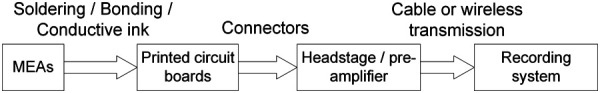
Flowchart of MEA packaging process
Packaging is the necessary process to facilitate the interconnections from recording sites on the electrodes all the way to the head stages/preamplifier, usually through microconnectors used [176]. Microwires or MEMS-based probes are connected to PCB pads by soldering [2,173], wire bonding [177], or conductive epoxies [178–180]. Given the specific recording system configuration, the PCBs involved could be either rigid or flexible, in the form of a single stage or multiple stages. The back end of the PCB should be a connector matching the preamplifier/head stage hardware [181]. Due to the headstage weight and size limit and high channel count requirements, most connectors used for MEAs are of very compact size. Popular commercially available connectors include board-to-board connectors (Samtec® connectors by Samtec Inc., New Albany, IN), zero impact force connectors (Hirose® connectors by Hirose Electric Group, Tokyo, Japan), D-sub connectors (Amphenol® connectors by Amphenol Corporation, Wallingford, CT), micro/nano connectors (Omnetics Nano Strip Connector series by Omnetics Connector Corporation, Minneapolis MN) and even wireless connectors [182–184]. These connectors have low connect-and-disconnect forces, thus mitigating the impact of the plugging/unplugging process on the recording performance. For commercial probes that are linked to flexible cables such as polyimide cables, the connections between flexible parts and the probes can be established by ultrasonic flip chip bonding [175], or simply soldering through conductive paint or manually. Biocompatible epoxy or other types of adhesives are normally used to bond parts together. Besides conventional connectors, the integrated circuits can be directly attached to the probes using wire bonding [185], flip-chip bonding with anisotropically conductive adhesive [186], and through-silicon vias [187].
Before in vivo use, MEAs are sealed with epoxy and sterilized by dipping in alcohol [188,189]. Besides the implanted probe, the head stage is another critical component in the entire electrophysiology system. The head stage stabilizes the microelectrodes in recordings and serves as the first stage for identifying signals [190]. Commercial head stages and recording systems such as SmartLink (NeuroNexus Technologies, Inc, Ann Arbor, MI), OmniPlex® (Plexon Inc, Dallas, TX), or Intan RHD models series (Intan Technologies, Los Angeles, CA) are commonly used in neuroscience for in vivo recordings. The head stages are usually set on the animals after implantation and only connected to the recording system when signals are required. For chronic in vivo recordings, wireless MEA recording systems could also be utilized. Without any animal-carrying headstage, the backside of the MEA is attached to an inductive coupling coil to create the wireless link [185]. With no wires needed, the signals from the recording will be sent wirelessly to the radio receiver, using power from a battery. Recently, wireless battery-free implantable MEAs have been reported by Ausra et al. [191] and Burton et al. [192]. The battery-free wireless MEA relies on the excitation of fluorescence. The overall system is further reduced, enabling smaller animal studies, such as adolescent mice for optogenetics.
6 Conclusion And Future Outlook
This paper presents an overview of various implantable MEAs for neural recording and stimulation purposes, from conventional MEAs to state-of-the-art novel designs. The corresponding manufacturing approaches are primarily reviewed in order to advance the future fabrication of next-generation neural MEAs. Technological advancements in micro/nanofabrication and new materials development have greatly facilitated the design and development of high electrode density, ultra-flexible neural MEAs since the 1950s. In the review, we summarize manufacturing processes for three conventional neural MEAs and other novel designs derived from these three types, including microwire, silicon-based MEAs (Utah Array and Michigan Probe), and flexible neural MEAs. Each type of MEA has its unique advantages, yet with apparent drawbacks. To fulfill the long-term vision of large-scale high-density brain-wide chronic recordings in freely moving animals, including the ambitious goal of the BRAIN initiative to record 1 million neurons simultaneously, we believe manufacturing technology development is needed in the following aspects:
Miniaturized-sized microelectrodes: To enable ultra-high channel counts, each channel has to be ultra-small wire delivering reliable electrical connection over time while flying under the radar of our immunization system.
Electrode material flexibility: For chronic recording performances, flexible electrode materials similar to the low modulus brain tissue property are critical for minimized brain tissue trauma and the related immune response.
Better biocompatibility and longer lifespan: The MEAs need to stay biocompatible and stable through months and even years of their recording lifespan.
Fabrication automation: Many manufacturing steps nowadays are still labor intensive, and the quality highly depends on the operator's skill and personal judgment. To lower the overall MEA cost as well as to ensure the accuracy, repeatability, and overall quality of the MEAs fabricated, automation efforts should be taken to use machine-controlled actuators to conduct most manufacturing steps including assembly and packaging.
Balance between resolution and cost: Even though the complex CMOS fabrication processes allow a high-resolution and high-density neural MEA, they highly rely on advanced manufacturing equipment and cleanroom facilities. The facility requirements also make the fabrication of customized neural MEAs challenging and high expense. Nowadays, more and more research groups explore cheaper and more agile manufacturing approaches to fabricate novel and customizable neural MEAs, such as 3D printing, screen printing, and automatic assembly of microwire MEAs, etc. At the same time, affordable manufacturing processes are usually limited by relatively low resolution, which limits the electrode density. Thus, it is still necessary to find a novel or hybrid manufacturing method to fabricate the next-generation neural MEA with ultra-flexibility, high electrode density, and a small footprint.
Acknowledgment
This research was previously presented at the 2023 Manufacturing Science and Engineering Conference (MSEC2023).
The content is solely the responsibility of the authors and does not necessarily represent the official views of the National Institutes of Health.
Images were reprinted with permission from their original resources.
Data Availability Statement
The datasets generated and supporting the findings of this article are obtainable from the corresponding author upon reasonable request.
Funding Data
National Institutes of Health (NIH) (Award No. R21MH120465; Funder ID: 10.13039/100000025).
References
- [1]. Biran, R. , Martin, D. C. , and Tresco, P. A. , 2005, “ Neuronal Cell Loss Accompanies the Brain Tissue Response to Chronically Implanted Silicon Microelectrode Arrays,” Exp. Neurol., 195(1), pp. 115–126. 10.1016/j.expneurol.2005.04.020 [DOI] [PubMed] [Google Scholar]
- [2]. Vitale, F. , Summerson, S. R. , Aazhang, B. , Kemere, C. , and Pasquali, M. , 2015, “ Neural Stimulation and Recording With Bidirectional, Soft Carbon Nanotube Fiber Microelectrodes,” ACS Nano, 9(4), pp. 4465–4474. 10.1021/acsnano.5b01060 [DOI] [PubMed] [Google Scholar]
- [3]. Qing, B. , and Wise, K. D. , 2001, “ Single-Unit Neural Recording With Active Microelectrode Arrays,” IEEE Trans. Biomed. Eng., 48(8), pp. 911–920. 10.1109/10.936367 [DOI] [PubMed] [Google Scholar]
- [4]. Vöröslakos, M. , Petersen, P. C. , Vöröslakos, B. , and Buzsáki, G. , 2021, “ Metal Microdrive and Head Cap System for Silicon Probe Recovery in Freely Moving Rodent,” eLife, 10, p. e65859. 10.7554/eLife.65859 [DOI] [PMC free article] [PubMed] [Google Scholar]
- [5]. Jefferys, J. G. , 1995, “ Nonsynaptic Modulation of Neuronal Activity in the Brain: electric Currents and Extracellular Ions,” Physiol. Rev., 75(4), pp. 689–723. 10.1152/physrev.1995.75.4.689 [DOI] [PubMed] [Google Scholar]
- [6]. Szostak, K. M. , Grand, L. , and Constandinou, T. G. , 2017, “ Neural Interfaces for Intracortical Recording: Requirements, Fabrication Methods, and Characteristics,” Front. Neurosci., 11, p. 665.https://www.frontiersin.org/articles/10.3389/fnins.2017.00665/full [DOI] [PMC free article] [PubMed] [Google Scholar]
- [7]. Veliev, F. , Han, Z. , Kalita, D. , Briançon-Marjollet, A. , Bouchiat, V. , and Delacour, C. , 2017, “ Recording Spikes Activity in Cultured Hippocampal Neurons Using Flexible or Transparent Graphene Transistors,” Front. Neurosci., 11 , p. 466. 10.3389/fnins.2017.00466 [DOI] [PMC free article] [PubMed] [Google Scholar]
- [8]. Peyrache, A. , Dehghani, N. , Eskandar, E. N. , Madsen, J. R. , Anderson, W. S. , Donoghue, J. A. , Hochberg, L. R. , Halgren, E. , Cash, S. S. , and Destexhe, A. , 2012, “ Spatiotemporal Dynamics of Neocortical Excitation and Inhibition During Human Sleep,” Proc. Natl. Acad. Sci., 109(5), pp. 1731–1736. 10.1073/pnas.1109895109 [DOI] [PMC free article] [PubMed] [Google Scholar]
- [9]. Lee, D. , Lee, G. , Kwon, D. , Lee, S. , Kim, Y. , and Kim, J. , 2018, “ Flexon: A Flexible Digital Neuron for Efficient Spiking Neural Network Simulations,” Proceedings of ACM/IEEE 45th Annual International Symposium on Computer Architecture (ISCA), Los Angeles, CA, June 1–6, pp. 275–288. 10.1109/ISCA.2018.00032 [DOI] [Google Scholar]
- [10]. Wellman, S. M. , Eles, J. R. , Ludwig, K. A. , Seymour, J. P. , Michelson, N. J. , McFadden, W. E. , Vazquez, A. L. , and Kozai, T. D. Y. , 2018, “ A Materials Roadmap to Functional Neural Interface Design,” Adv. Funct. Mater., 28(12), p. 1701269. 10.1002/adfm.201701269 [DOI] [PMC free article] [PubMed] [Google Scholar]
- [11]. Verkhratsky, A. , Krishtal, O. A. , and Petersen, O. H. , 2006, “ From Galvani to Patch Clamp: The Development of Electrophysiology,” Pflügers Arch., 453(3), pp. 233–247. 10.1007/s00424-006-0169-z [DOI] [PubMed] [Google Scholar]
- [12]. Hodgkin, A. , 1979, “ Edgar Douglas Adrian, Baron Adrian of Cambridge, 30 November 1889 - 4 August 1977,” Biograph. Memoirs Fellows R. Soc., 25, pp. 1–73. 10.1098/rsbm.1979.0002 [DOI] [PubMed] [Google Scholar]
- [13]. Woldring, S. , and Dirken, M. N. , 1950, “ Spontaneous Unit-Activity in the Superficial Cortical Layers,” Acta Physiol. Pharmacol. Neerl, 1(3), pp. 369–379. [PubMed] [Google Scholar]
- [14]. Strumwasser, F. , 1958, “ Long-Term Recording From Single Neurons in Brain of Unrestrained Mammals,” Science, 127(3296), pp. 469–470. 10.1126/science.127.3296.469 [DOI] [PubMed] [Google Scholar]
- [15]. Hubel, D. H. , and Wiesel, T. N. , 1965, “ Receptive Fields and Functional Architecture in Two Nonstriate Visual Areas (18 and 19) of the Cat,” J. Neurophysiol., 28(2), pp. 229–289. 10.1152/jn.1965.28.2.229 [DOI] [PubMed] [Google Scholar]
- [16]. Hubel, D. H. , and Wiesel, T. N. , 1959, “ Receptive Fields of Single Neurones in the Cat's Striate Cortex,” J. Physiol., 148(3), pp. 574–591. 10.1113/jphysiol.1959.sp006308 [DOI] [PMC free article] [PubMed] [Google Scholar]
- [17]. Lehew, G. , and Nicolelis, M. A. , 2008, “ State-of-the-Art Microwire Array Design for Chronic Neural Recordings in Behaving Animals,” Methods Neural Ensemble Record., 2, pp. 361–371. [PubMed] [Google Scholar]
- [18]. Obaid, A. , Hanna, M.-E. , Wu, Y.-W. , Kollo, M. , Racz, R. , Angle, M. R. , Müller, J. , et al., 2020, “ Massively Parallel Microwire Arrays Integrated With CMOS Chips for Neural Recording,” Sci. Adv., 6(12), p. eaay2789. 10.1126/sciadv.aay2789 [DOI] [PMC free article] [PubMed] [Google Scholar]
- [19]. Yi, D. , Hartner, J. P. , Ung, B. S. , Zhu, H. L. , Watson, B. O. , and Chen, L. , 2022, “ 3D Printed Skull Cap and Benchtop Fabricated Microwire-Based Microelectrode Array for Custom Rat Brain Recordings,” Bioengineering, 9(10), p. 550. 10.3390/bioengineering9100550 [DOI] [PMC free article] [PubMed] [Google Scholar]
- [20]. Kellis, S. , Greger, B. , Hanrahan, S. , House, P. , and Brown, R. , 2011, “ Platinum Microwire for Subdural Electrocorticography Over Human Neocortex: Millimeter-Scale Spatiotemporal Dynamics,” Proceedings of Annual International Conference of the IEEE Engineering in Medicine and Biology Society, Boston, MA, Aug. 30–Sept. 3, pp. 4761–4765. 10.1109/IEMBS.2011.6091179 [DOI] [PubMed] [Google Scholar]
- [21]. Chen, L. , Hartner, J. , Van Dyke, D. , Dong, T. , Watson, B. , and Shih, A. , 2019, “ Custom Skull Cap With Precision Guides for Deep Insertion of Cellular-Scale Microwire Into Rat Brain,” ASME Paper No. MSEC2019-2967. 10.1115/MSEC2019-2967 [DOI] [Google Scholar]
- [22]. Gillis, W. F. , Lissandrello, C. A. , Shen, J. , Pearre, B. W. , Mertiri, A. , Deku, F. , Cogan, S. , Holinski, B. J. , Chew, D. J. , White, A. E. , Otchy, T. M. , and Gardner, T. J. , 2018, “ Carbon Fiber on Polyimide Ultra-Microelectrodes,” J. Neural Eng., 15(1), p. 016010. 10.1088/1741-2552/aa8c88 [DOI] [PMC free article] [PubMed] [Google Scholar]
- [23]. Mendrela, A. E. , Kim, K. , English, D. , McKenzie, S. , Seymour, J. P. , Buzsáki, G. , and Yoon, E. , 2018, “ A High-Resolution Opto-Electrophysiology System With a Miniature Integrated Headstage,” IEEE Trans. Biomed. Circuits Syst., 12(5), pp. 1065–1075. 10.1109/TBCAS.2018.2852267 [DOI] [PMC free article] [PubMed] [Google Scholar]
- [24]. Wise, K. D. , Angell, J. B. , and Starr, A. , 1970, “ An Integrated-Circuit Approach to Extracellular Microelectrodes,” IEEE Trans. Biomed. Eng., BME-17(3), pp. 238–247. 10.1109/TBME.1970.4502738 [DOI] [PubMed] [Google Scholar]
- [25]. Qing, B. , Wise, K. D. , and Anderson, D. J. , 2000, “ A High-Yield Microassembly Structure for Three-Dimensional Microelectrode Arrays,” IEEE Trans. Biomed. Eng., 47(3), pp. 281–289. 10.1109/10.827288 [DOI] [PubMed] [Google Scholar]
- [26]. Campbell, P. K. , Jones, K. E. , Huber, R. J. , Horch, K. W. , and Normann, R. A. , 1991, “ A Silicon-Based, Three-Dimensional Neural Interface: manufacturing Processes for an Intracortical Electrode Array,” IEEE Trans. Biomed. Eng., 38(8), pp. 758–768. 10.1109/10.83588 [DOI] [PubMed] [Google Scholar]
- [27]. Nordhausen, C. T. , Maynard, E. M. , and Normann, R. A. , 1996, “ Single Unit Recording Capabilities of a 100 Microelectrode Array,” Brain Res., 726(1-2), pp. 129–140. 10.1016/0006-8993(96)00321-6 [DOI] [PubMed] [Google Scholar]
- [28]. Bennett, C. , Mohammed, F. , Álvarez-Ciara, A. , Nguyen, M. A. , Dietrich, W. D. , Rajguru, S. M. , Streit, W. J. , and Prasad, A. , 2019, “ Neuroinflammation, Oxidative Stress, and Blood-Brain Barrier (BBB) Disruption in Acute Utah Electrode Array Implants and the Effect of Deferoxamine as an Iron Chelator on Acute Foreign Body Response,” Biomaterials, 188, pp. 144–159. 10.1016/j.biomaterials.2018.09.040 [DOI] [PMC free article] [PubMed] [Google Scholar]
- [29]. Christensen, M. B. , Pearce, S. M. , Ledbetter, N. M. , Warren, D. J. , Clark, G. A. , and Tresco, P. A. , 2014, “ The Foreign Body Response to the Utah Slant Electrode Array in the Cat Sciatic Nerve,” Acta Biomater., 10(11), pp. 4650–4660. 10.1016/j.actbio.2014.07.010 [DOI] [PubMed] [Google Scholar]
- [30]. Rousche, P. J. , Pellinen, D. S. , Pivin, D. P. , Williams, J. C. , Vetter, R. J. , and Kipke, D. R. , 2001, “ Flexible Polyimide-Based Intracortical Electrode Arrays With Bioactive Capability,” IEEE Trans. Biomed. Eng., 48(3), pp. 361–371. 10.1109/10.914800 [DOI] [PubMed] [Google Scholar]
- [31]. Hubel, D. H. , 1957, “ Tungsten Microelectrode for Recording From Single Units,” Science, 125(3247), pp. 549–550. 10.1126/science.125.3247.549 [DOI] [PubMed] [Google Scholar]
- [32]. Li, L. , Jiang, C. , Duan, W. , Wang, Z. , Zhang, F. , He, C. , Long, T. , and Li, L. , 2022, “ Electrochemical and Biological Performance of Hierarchical Platinum-Iridium Electrodes Structured by a Femtosecond Laser,” Microsyst. Nanoeng., 8(1), p. 96. 10.1038/s41378-022-00433-8 [DOI] [PMC free article] [PubMed] [Google Scholar]
- [33]. Guitchounts, G. , and Cox, D. , 2020, “ 64-Channel Carbon Fiber Electrode Arrays for Chronic Electrophysiology,” Sci. Rep., 10(1), p. 3830. 10.1038/s41598-020-60873-y [DOI] [PMC free article] [PubMed] [Google Scholar]
- [34]. Welle, E. J. , Patel, P. R. , Woods, J. E. , Petrossians, A. , della Valle, E. , Vega-Medina, A. , Richie, J. M. , Cai, D. , Weiland, J. D. , and Chestek, C. A. , 2020, “ Ultra-Small Carbon Fiber Electrode Recording Site Optimization and Improved In Vivo Chronic Recording Yield,” J. Neural Eng., 17(2), p. 026037. 10.1088/1741-2552/ab8343 [DOI] [PMC free article] [PubMed] [Google Scholar]
- [35]. Sahasrabuddhe, K. , Khan, A. A. , Singh, A. P. , Stern, T. M. , Ng, Y. , Tadić, A. , Orel, P. , et al., 2020, “ The Argo: A High Channel Count Recording System for Neural Recording In Vivo,” J. Neural Eng., 18(1), p. 015002. 10.1088/1741-2552/abd0ce [DOI] [PMC free article] [PubMed] [Google Scholar]
- [36]. Merritt, C. D. , and Justus, B. L. , 2003, “ Fabrication of Microelectrode Arrays Having High-Aspect-Ratio Microwires,” Chem. Mater., 15(13), pp. 2520–2526. 10.1021/cm020821y [DOI] [Google Scholar]
- [37]. Pei, W. , Zhao, H. , Zhao, S. , Fang, X. , Chen, S. , Gui, Q. , Tang, R. , Chen, Y. , Hong, B. , Gao, X. , and Chen, H. , 2014, “ Silicon-Based Wire Electrode Array for Neural Interfaces,” J. Micromech. Microeng., 24(9), p. 095015. 10.1088/0960-1317/24/9/095015 [DOI] [Google Scholar]
- [38]. Saleh, M. S. , Ritchie, S. M. , Nicholas, M. A. , Gordon, H. L. , Hu, C. , Jahan, S. , Yuan, B. , Bezbaruah, R. , Reddy, J. W. , Ahmed, Z. , Chamanzar, M. , Yttri, E. A. , and Panat, R. P. , 2022, “ CMU Array: A 3D Nanoprinted, Fully Customizable High-Density Microelectrode Array Platform,” Sci. Adv., 8(40), p. eabj4853. 10.1126/sciadv.abj4853 [DOI] [PMC free article] [PubMed] [Google Scholar]
- [39]. Jarfors, A. E. W. , and Seifeddine, S. , 2013, “ Metal Casting,” Handbook of Manufacturing Engineering and Technology, Nee A., ed., Springer London, London, pp. 1–90. [Google Scholar]
- [40]. Cantor, B. , Chang, I. T. H. , Knight, P. , and Vincent, A. J. B. , 2004, “ Microstructural Development in Equiatomic Multicomponent Alloys,” Mater. Sci. Eng.: A, 375–377, pp. 213–218. 10.1016/j.msea.2003.10.257 [DOI] [Google Scholar]
- [41]. Shen, Q. , Kong, X. , and Chen, X. , 2021, “ Fabrication of Bulk Al-Co-Cr-Fe-Ni High-Entropy Alloy Using Combined Cable Wire Arc Additive Manufacturing (CCW-AAM): Microstructure and Mechanical Properties,” J. Mater. Sci. Technol., 74, pp. 136–142. 10.1016/j.jmst.2020.10.037 [DOI] [Google Scholar]
- [42]. Jia, Z. , Hao, S. , Wen, J. , Li, S. , Peng, W. , Huang, R. , and Xu, X. , 2020, “ Electrochemical Fabrication of Metal–Organic Frameworks Membranes and Films: A Review,” Microporous Mesoporous Mater., 305, p. 110322. 10.1016/j.micromeso.2020.110322 [DOI] [Google Scholar]
- [43]. Perumal, V. , Amil, N. , Aiman, N. , and Hashim, U. , 2013, “ Fabrication and Characterization of Metal Microwire Transducer for Biochip Application,” Proceedings of RSM IEEE Regional Symposium on Micro and Nanoelectronics, Daerah Langkawi, Malaysia, Sept. 25–27, pp. 29–32. 10.1109/RSM.2013.6706465 [DOI] [Google Scholar]
- [44]. Pérez-Díaz, O. , Quiroga-González, E. , Hansen, S. , Silva-González, N. R. , Carstensen, J. , and Adelung, R. , 2019, “ Fabrication of Silicon Microwires by a Combination of Chemical Etching Steps and Their Analysis as Anode Material in Li-Ion Batteries,” Mater. Technol., 34(13), pp. 785–791. 10.1080/10667857.2019.1629059 [DOI] [Google Scholar]
- [45]. Chen, M. , Mu, L. , Wang, S. , Cao, X. , Liang, S. , Wang, Y. , She, G. , Yang, J. , Wang, Y. , and Shi, W. , 2020, “ A Single Silicon Nanowire-Based Ratiometric Biosensor for Ca2+ at Various Locations in a Neuron,” ACS Chem. Neurosci., 11(9), pp. 1283–1290. 10.1021/acschemneuro.0c00041 [DOI] [PubMed] [Google Scholar]
- [46]. Woods, J. E. , Welle, E. J. , Chen, L. , Richie, J. M. , Patel, P. R. , and Chestek, C. A. , 2020, “ Bending Properties of Materials for Peripheral Nerve Interfaces,” Proceedings of IEEE 15th International Conference on Nano/Micro Engineered and Molecular System (NEMS), San Diego, CA, Sept. 27–30, pp. 407–412. 10.1109/NEMS50311.2020.9265629 [DOI] [Google Scholar]
- [47]. Vafaiee, M. , Mohammadpour, R. , Vossoughi, M. , Asadian, E. , Janahmadi, M. , and Sasanpour, P. , 2021, “ Carbon Nanotube Modified Microelectrode Array for Neural Interface,” Front. Bioeng. Biotechnol., 8, p. 582713. 10.3389/fbioe.2020.582713 [DOI] [PMC free article] [PubMed] [Google Scholar]
- [48]. Hejazi, M. , Tong, W. , Ibbotson, M. R. , Prawer, S. , and Garrett, D. J. , 2021, “ Advances in Carbon-Based Microfiber Electrodes for Neural Interfacing,” Front. Neurosci., 15, p. 658703. 10.3389/fnins.2021.658703 [DOI] [PMC free article] [PubMed] [Google Scholar]
- [49]. Santos, R. M. , Lourenço, C. F. , Piedade, A. P. , Andrews, R. , Pomerleau, F. , Huettl, P. , Gerhardt, G. A. , Laranjinha, J. , and Barbosa, R. M. , 2008, “ A Comparative Study of Carbon Fiber-Based Microelectrodes for the Measurement of Nitric Oxide in Brain Tissue,” Biosens. Bioelectron., 24(4), pp. 704–709. 10.1016/j.bios.2008.06.034 [DOI] [PubMed] [Google Scholar]
- [50]. Yusof, N. , and Ismail, A. F. , 2012, “ Post Spinning and Pyrolysis Processes of Polyacrylonitrile (PAN)-Based Carbon Fiber and Activated Carbon Fiber: A Review,” J. Anal. Appl. Pyrol., 93, pp. 1–13. 10.1016/j.jaap.2011.10.001 [DOI] [Google Scholar]
- [51]. Frank, E. , Hermanutz, F. , and Buchmeiser, M. R. , 2012, “ Carbon Fibers: Precursors, Manufacturing, and Properties,” Macromol. Mater. Eng., 297(6), pp. 493–501. 10.1002/mame.201100406 [DOI] [Google Scholar]
- [52]. Richie, J. M. , Patel, P. R. , Welle, E. J. , Dong, T. , Chen, L. , Shih, A. J. , and Chestek, C. A. , 2021, “ Open-Source Toolkit: Benchtop Carbon Fiber Microelectrode Array for Nerve Recording,” J. Vis. Exp., (176), p. e63099. 10.3791/63099 [DOI] [PMC free article] [PubMed] [Google Scholar]
- [53]. Guitchounts, G. , Markowitz, J. E. , Liberti, W. A. , and Gardner, T. J. , 2013, “ A Carbon-Fiber Electrode Array for Long-Term Neural Recording,” J. Neural Eng., 10(4), p. 046016. 10.1088/1741-2560/10/4/046016 [DOI] [PMC free article] [PubMed] [Google Scholar]
- [54]. Patel, P. R. , Popov, P. , Caldwell, C. M. , Welle, E. J. , Egert, D. , Pettibone, J. R. , Roossien, D. H. , Becker, J. B. , Berke, J. D. , Chestek, C. A. , and Cai, D. , 2020, “ High Density Carbon Fiber Arrays for Chronic Electrophysiology, Fast Scan Cyclic Voltammetry, and Correlative Anatomy,” J. Neural Eng., 17(5), p. 056029. 10.1088/1741-2552/abb1f6 [DOI] [PubMed] [Google Scholar]
- [55]. Yi, W. , Chen, C. , Feng, Z. , Xu, Y. , Zhou, C. , Masurkar, N. , Cavanaugh, J. , and Ming-Cheng Cheng, M. , 2015, “ A Flexible and Implantable Microelectrode Arrays Using High-Temperature Grown Vertical Carbon Nanotubes and a Biocompatible Polymer Substrate,” Nanotechnology, 26(12), p. 125301. 10.1088/0957-4484/26/12/125301 [DOI] [PubMed] [Google Scholar]
- [56]. Behabtu, N. , Young, C. C. , Tsentalovich, D. E. , Kleinerman, O. , Wang, X. , Ma, A. W. K. , Bengio, E. A. , et al., 2013, “ Strong, Light, Multifunctional Fibers of Carbon Nanotubes With Ultrahigh Conductivity,” Science, 339(6116), pp. 182–186. 10.1126/science.1228061 [DOI] [PubMed] [Google Scholar]
- [57]. Si, B. , and Song, E. , 2018, “ Recent Advances in the Detection of Neurotransmitters,” Chemosensors, 6(1), p. 1. 10.3390/chemosensors6010001 [DOI] [Google Scholar]
- [58]. Zeng, J. , Xu, R. , Jiao, L. , Wang, Y. , Chen, L. , Windle, C. D. , Ding, X. , Zhang, Z. , Han, Q. , and Qu, L. , 2019, “ A 3D-Graphene Fiber Electrode Embedded With Nitrogen-Rich-Carbon-Coated ZIF-67 for the Ultrasensitive Detection of Adrenaline,” J. Mater. Chem. B, 7(35), pp. 5291–5295. 10.1039/C9TB01223K [DOI] [PubMed] [Google Scholar]
- [59]. Zheng, Y. , 2017, Design and Fabrication of a Highly Flexible Neural Electrode, Case Western Reserve University, Cleveland, OH. [Google Scholar]
- [60]. Zhao, S. , Liu, X. , Xu, Z. , Ren, H. , Deng, B. , Tang, M. , Lu, L. , Fu, X. , Peng, H. , Liu, Z. , and Duan, X. , 2016, “ Graphene Encapsulated Copper Microwires as Highly MRI Compatible Neural Electrodes,” Nano Lett., 16(12), pp. 7731–7738. 10.1021/acs.nanolett.6b03829 [DOI] [PubMed] [Google Scholar]
- [61]. Apollo, N. V. , Maturana, M. I. , Tong, W. , Nayagam, D. A. , Shivdasani, M. N. , Foroughi, J. , Wallace, G. G. , Prawer, S. , Ibbotson, M. R. , and Garrett, D. J. , 2015, “ Soft, Flexible Freestanding Neural Stimulation and Recording Electrodes Fabricated From Reduced Graphene Oxide,” Adv. Funct. Mater., 25(23), pp. 3551–3559. 10.1002/adfm.201500110 [DOI] [Google Scholar]
- [62]. Cheng, H. , Hu, C. , Zhao, Y. , and Qu, L. , 2014, “ Graphene Fiber: A New Material Platform for Unique Applications,” NPG Asia Mater., 6(7), pp. e113–e113. 10.1038/am.2014.48 [DOI] [Google Scholar]
- [63]. Bartholomew, G. A. , 1962, “ Method and Apparatus for Coating Metal Strip and Wire,” Google Patents No. 3,019,126. [Google Scholar]
- [64]. Jorfi, M. , Skousen, J. L. , Weder, C. , and Capadona, J. R. , 2015, “ Progress Towards Biocompatible Intracortical Microelectrodes for Neural Interfacing Applications,” J. Neural Eng., 12(1), p. 011001. 10.1088/1741-2560/12/1/011001 [DOI] [PMC free article] [PubMed] [Google Scholar]
- [65]. Weltman, A. , Yoo, J. , and Meng, E. , 2016, “ Flexible, Penetrating Brain Probes Enabled by Advances in Polymer Microfabrication,” Micromachines (Basel), 7(10), p. 180. 10.3390/mi7100180 [DOI] [PMC free article] [PubMed] [Google Scholar]
- [66]. O'Doherty, J. , Lebedev, M. , Hanson, T. , Fitzsimmons, N. , and Nicolelis, M. , 2009, “ A Brain-Machine Interface Instructed by Direct Intracortical Microstimulation,” Front. Integr. Neurosci., 3, p. 803. 10.3389/neuro.07.020.2009 [DOI] [PMC free article] [PubMed] [Google Scholar]
- [67]. Westby, G. W. M. , and Wang, H. , 1997, “ A Floating Microwire Technique for Multichannel Chronic Neural Recording and Stimulation in the Awake Freely Moving Rat,” J. Neurosci. Methods, 76(2), pp. 123–133. 10.1016/S0165-0270(97)00088-5 [DOI] [PubMed] [Google Scholar]
- [68]. Mardani, R. , Shahmirzaee, H. , Ershadifar, H. , and Vahdani, M. R. , 2017, “ Electrodeposition of Ni32Fe48Mo20 and Ni52Fe33W15 Alloy Film on Cu Microwire From Ionic Liquid Containing Plating Bath,” Surf. Coat. Technol., 324, pp. 281–287. 10.1016/j.surfcoat.2017.05.087 [DOI] [Google Scholar]
- [69]. Loeb, G. E. , Bak, M. J. , Salcman, M. , and Schmidt, E. M. , 1977, “ Parylene as a Chronically Stable, Reproducible Microelectrode Insulator,” IEEE Trans. Biomed. Eng., BME-24(2), pp. 121–128. 10.1109/TBME.1977.326115 [DOI] [PubMed] [Google Scholar]
- [70]. Kleinbach, E. , and Riede, T. , 1995, “ Coating of Solids,” Chem. Eng. Process., 34(3), pp. 329–337. 10.1016/0255-2701(94)04021-4 [DOI] [Google Scholar]
- [71]. Chen, Y. , Zhang, J. , Zhou, J. , Chu, Y. , Zhou, B. , Wu, X. , and Huang, J. , 2018, “ Long-Term Stable and Tunable High-Performance Photodetectors Based on Perovskite Microwires,” Adv. Opt. Mater., 6(22), p. 1800469. 10.1002/adom.201800469 [DOI] [Google Scholar]
- [72]. Salcman, M. , and Bak, M. J. , 1973, “ Design, Fabrication, and In Vivo Behavior of Chronic Recording Intracortical Microelectrodes,” IEEE Trans. Biomed. Eng., BME-20(4), pp. 253–260. 10.1109/TBME.1973.324189 [DOI] [PubMed] [Google Scholar]
- [73]. Palmer, C. , 1978, “ A Microwire Technique for Recording Single Neurons in Unrestrained Animals,” Brain Res. Bull., 3(3), pp. 285–289. 10.1016/0361-9230(78)90129-6 [DOI] [PubMed] [Google Scholar]
- [74]. Kaltenbach, J. A. , and Gerstein, G. L. , 1986, “ A Rapid Method for Production of Sharp Tips on Preinsulated Microwires,” J. Neurosci. Methods, 16(4), pp. 283–288. 10.1016/0165-0270(86)90053-1 [DOI] [PubMed] [Google Scholar]
- [75]. Cheung, K. C. , Djupsund, K. , Dan, Y. , and Lee, L. P. , 2003, “ Implantable Multichannel Electrode Array Based on SOI Technology,” J. Microelectromech. Syst., 12(2), pp. 179–184. 10.1109/JMEMS.2003.809962 [DOI] [Google Scholar]
- [76]. Chen, L. , Hartner, J. P. , Dong, T. K. , Li, A. D. R. , Watson, B. O. , and Shih, A. J. , 2021, “ Flexible High-Resolution Force and Dimpling Measurement System for Pia and Dura Penetration During In Vivo Microelectrode Insertion Into Rat Brain,” IEEE Trans. Biomed. Eng., 68(8), pp. 2602–2612. 10.1109/TBME.2021.3070781 [DOI] [PMC free article] [PubMed] [Google Scholar]
- [77]. Schmidt, E. M. , Bak, M. J. , and Christensen, P. , 1995, “ Laser Exposure of Parylene-C Insulated Microelectrodes,” J. Neurosci. Methods, 62(1-2), pp. 89–92. 10.1016/0165-0270(95)00060-7 [DOI] [PubMed] [Google Scholar]
- [78]. Budai, D. , and Molnár, Z. , 2001, “ Novel Carbon Fiber Microeletrodes for Extracellular Electrophysiology,” Acta Biol. Szegediensis, 45(1-4), pp. 65–73.https://abs.bibl.uszeged.hu/index.php/abs/article/view/2187 [Google Scholar]
- [79]. Ho, K. H. , and Newman, S. T. , 2003, “ State of the Art Electrical Discharge Machining (EDM),” Int. J. Mach. Tools Manuf., 43(13), pp. 1287–1300. 10.1016/S0890-6955(03)00162-7 [DOI] [Google Scholar]
- [80]. Kollo, M. , Racz, R. , Hanna, M.-E. , Obaid, A. , Angle, M. R. , Wray, W. , Kong, Y. , Müller, J. , Hierlemann, A. , Melosh, N. A. , and Schaefer, A. T. , 2020, “ CHIME: CMOS-Hosted In Vivo Microelectrodes for Massively Scalable Neuronal Recordings,” Front. Neurosci., 14, p. 834. 10.3389/fnins.2020.00834 [DOI] [PMC free article] [PubMed] [Google Scholar]
- [81]. Dong, T. , Chen, L. , and Shih, A. , 2020, “ Laser Sharpening of Carbon Fiber Microelectrode Arrays for Brain Recording,” J. Micro Nanomanuf., 8(4), p. 041013. 10.1115/1.4049780 [DOI] [PMC free article] [PubMed] [Google Scholar]
- [82]. Shah Idil, A. , and Donaldson, N. , 2018, “ The Use of Tungsten as a Chronically Implanted Material,” J. Neural Eng., 15(2), p. 021006. 10.1088/1741-2552/aaa502 [DOI] [PubMed] [Google Scholar]
- [83]. Sharp, A. A. , Ortega, A. M. , Restrepo, D. , Curran-Everett, D. , and Gall, K. , 2009, “ In Vivo Penetration Mechanics and Mechanical Properties of Mouse Brain Tissue at Micrometer Scales,” IEEE Trans. Biomed. Eng., 56(1), pp. 45–53. 10.1109/TBME.2008.2003261 [DOI] [PMC free article] [PubMed] [Google Scholar]
- [84]. Chang, W.-T. , Hwang, I.-S. , Chang, M.-T. , Lin, C.-Y. , Hsu, W.-H. , and Hou, J.-L. , 2012, “ Method of Electrochemical Etching of Tungsten Tips With Controllable Profiles,” Rev. Sci. Instrum., 83(8), p. 083704. 10.1063/1.4745394 [DOI] [PubMed] [Google Scholar]
- [85]. Hanein, Y. , and Bareket-Keren, L. , 2013, “ Carbon Nanotube-Based Multi Electrode Arrays for Neuronal Interfacing: progress and Prospects,” Front. Neural Circuits, 6, p. 122. 10.3389/fncir.2012.00122 [DOI] [PMC free article] [PubMed] [Google Scholar]
- [86]. Jones, K. E. , Campbell, P. K. , and Normann, R. A. , 1992, “ A Glass/Silicon Composite Intracortical Electrode Array,” Ann. Biomed. Eng., 20(4), pp. 423–437. 10.1007/BF02368134 [DOI] [PubMed] [Google Scholar]
- [87]. Bhandari, R. , Negi, S. , Rieth, L. , Normann, R. A. , and Solzbacher, F. , 2008, “ A Novel Method of Fabricating Convoluted Shaped Electrode Arrays for Neural and Retinal Prostheses,” Sens. Actuators A: Phys., 145–146, pp. 123–130. 10.1016/j.sna.2007.10.072 [DOI] [PMC free article] [PubMed] [Google Scholar]
- [88]. Bhandari, R. , Negi, S. , and Solzbacher, F. , 2010, “ Wafer-Scale Fabrication of Penetrating Neural Microelectrode Arrays,” Biomed. Microdev., 12(5), pp. 797–807. 10.1007/s10544-010-9434-1 [DOI] [PubMed] [Google Scholar]
- [89]. Leber, M. , Körner, J. , Reiche, C. F. , Yin, M. , Bhandari, R. , Franklin, R. , Negi, S. , and Solzbacher, F. , 2019, “Advances in Penetrating Multichannel Microelectrodes Based on the Utah Array Platform,” Neural Interface: Frontiers and Applications, Zheng X., ed., Springer Singapore, Singapore, pp. 1–40. [DOI] [PubMed] [Google Scholar]
- [90]. Joshi-Imre, A. , Black, B. J. , Abbott, J. , Kanneganti, A. , Rihani, R. , Chakraborty, B. , Danda, V. R. , et al., 2019, “ Chronic Recording and Electrochemical Performance of Amorphous Silicon Carbide-Coated Utah Electrode Arrays Implanted in Rat Motor Cortex,” J. Neural Eng., 16(4), p. 046006. 10.1088/1741-2552/ab1bc8 [DOI] [PubMed] [Google Scholar]
- [91]. Rutishauser, U. , Aflalo, T. , Rosario, E. R. , Pouratian, N. , and Andersen, R. A. , 2018, “ Single-Neuron Representation of Memory Strength and Recognition Confidence in Left Human Posterior Parietal Cortex,” Neuron, 97(1), pp. 209–220. 10.1016/j.neuron.2017.11.029 [DOI] [PMC free article] [PubMed] [Google Scholar]
- [92]. Weiss, S. A. , Banks, G. P. , McKhann, G. M., Jr. , Goodman, R. R. , Emerson, R. G. , Trevelyan, A. J. , and Schevon, C. A. , 2013, “ Ictal High Frequency Oscillations Distinguish Two Types of Seizure Territories in Humans,” Brain, 136(12), pp. 3796–3808. 10.1093/brain/awt276 [DOI] [PMC free article] [PubMed] [Google Scholar]
- [93]. Hochberg, L. R. , Serruya, M. D. , Friehs, G. M. , Mukand, J. A. , Saleh, M. , Caplan, A. H. , Branner, A. , Chen, D. , Penn, R. D. , and Donoghue, J. P. , 2006, “ Neuronal Ensemble Control of Prosthetic Devices by a Human With Tetraplegia,” Nature, 442(7099), pp. 164–171. 10.1038/nature04970 [DOI] [PubMed] [Google Scholar]
- [94]. Armenta Salas, M. , Bashford, L. , Kellis, S. , Jafari, M. , Jo, H. , Kramer, D. , Shanfield, K. , Pejsa, K. , Lee, B. , Liu, C. Y. , and Andersen, R. A. , 2018, “ Proprioceptive and Cutaneous Sensations in Humans Elicited by Intracortical Microstimulation,” eLife, 7, p. e32904. 10.7554/eLife.32904 [DOI] [PMC free article] [PubMed] [Google Scholar]
- [95]. Normann, R. A. , Greger, B. A. , House, P. , Romero, S. F. , Pelayo, F. , and Fernandez, E. , 2009, “ Toward the Development of a Cortically Based Visual Neuroprosthesis,” J. Neural Eng., 6(3), p. 035001. 10.1088/1741-2560/6/3/035001 [DOI] [PMC free article] [PubMed] [Google Scholar]
- [96]. George, J. A. , Page, D. M. , Davis, T. S. , Duncan, C. C. , Hutchinson, D. T. , Rieth, L. W. , and Clark, G. A. , 2020, “ Long-Term Performance of Utah Slanted Electrode Arrays and Intramuscular Electromyographic Leads Implanted Chronically in Human Arm Nerves and Muscles,” J. Neural Eng., 17(5), p. 056042. 10.1088/1741-2552/abc025 [DOI] [PubMed] [Google Scholar]
- [97]. Abaya, T. V. F. , Diwekar, M. , Blair, S. , Tathireddy, P. , Rieth, L. , and Solzbacher, F. , 2012, “ 3D Waveguide Penetrating Arrays for Optical Neural Stimulation,” Proceedings of International Conference on Optical MEMS and Nanophotonics, Banff, AB, Canada, Aug. 6–9, pp. 216–217. 10.1109/OMEMS.2012.6318880 [DOI] [Google Scholar]
- [98]. Branner, A. , Stein, R. B. , and Normann, R. A. , 2001, “ Selective Stimulation of Cat Sciatic Nerve Using an Array of Varying-Length Microelectrodes,” J. Neurophysiol., 85(4), pp. 1585–1594. 10.1152/jn.2001.85.4.1585 [DOI] [PubMed] [Google Scholar]
- [99]. Campbell, P. K. , Jones, K. E. , and Normann, R. A. , 1990, “ A 100 Electrode Intracortical Array: structural Variability,” Biomed. Sci. Instrum., 26, pp. 161–165. [PubMed] [Google Scholar]
- [100]. Shandhi, M. M. H. , Leber, M. , Hogan, A. L. , Warren, D. J. , Bhandari, R. , and Negi, S. , 2017, “ Reusable High Aspect Ratio 3-D Nickel Shadow Mask,” J. Microelectromech. Syst., 26(2), pp. 376–384. 10.1109/JMEMS.2017.2654126 [DOI] [PMC free article] [PubMed] [Google Scholar]
- [101]. Mokwa, W. , Wessling, B. , and Schnakenberg, U. , 2007, “ Sputtered Iridium Oxide for Stimulation Electrode Coatings,” Proceedings of 29th Annual International Conference of the IEEE Engineering in Medicine and Biology Society, Lyon, France, Aug. 22–26, pp. 6047–6050. 10.1109/IEMBS.2007.4353727 [DOI] [PubMed] [Google Scholar]
- [102]. Woeppel, K. , Hughes, C. , Herrera, A. J. , Eles, J. R. , Tyler-Kabara, E. C. , Gaunt, R. A. , Collinger, J. L. , and Cui, X. T. , 2021, “ Explant Analysis of Utah Electrode Arrays Implanted in Human Cortex for Brain-Computer-Interfaces,” Front. Bioeng. Biotechnol., 9, p. 1137. 10.3389/fbioe.2021.759711 [DOI] [PMC free article] [PubMed] [Google Scholar]
- [103]. Xie, X. , Rieth, L. W. , Cardwell, R. , Sharma, R. , Yoo, J.-M. , Diweka, M. , Tathireddy, P. , and Solzbacher, F. , 2013, “ Bi-Layer Encapsulation of Utah Array Based Nerual Interfaces by Atomic Layer Deposited Al2O3 and Parylene C,” Transducers & Eurosensors XXVII: The 17th International Conference on Solid-State Sensors, Actuators and Microsystems (TRANSDUCERS & EUROSENSORS XXVII), Barcelona, Spain, June 16–20, pp. 1267–1270. 10.1109/Transducers.2013.6627006 [DOI] [Google Scholar]
- [104]. Fekete, Z. , 2015, “ Recent Advances in Silicon-Based Neural Microelectrodes and Microsystems: A Review,” Sens. Actuators B Chem., 215, pp. 300–315. 10.1016/j.snb.2015.03.055 [DOI] [Google Scholar]
- [105]. Rapeaux, A. B. , and Constandinou, T. G. , 2021, “ Implantable Brain Machine Interfaces: First-In-Human Studies, Technology Challenges and Trends,” Curr. Opin. Biotechnol., 72, pp. 102–111. 10.1016/j.copbio.2021.10.001 [DOI] [PubMed] [Google Scholar]
- [106]. Kindlundh, M. , Norlin, P. , and Hofmann, U. G. , 2004, “ A Neural Probe Process Enabling Variable Electrode Configurations,” Sens. Actuators B Chem., 102(1), pp. 51–58. 10.1016/j.snb.2003.10.009 [DOI] [Google Scholar]
- [107]. Peter, N. , Maria, K. , Aliette, M. , Ken, Y. , and Ulrich, G. H. , 2002, “ A 32-Site Neural Recording Probe Fabricated by DRIE of SOI Substrates,” J. Micromech. Microeng., 12(4), p. 414. 10.1088/0960-1317/12/4/312 [DOI] [Google Scholar]
- [108]. Najafi, K. , Wise, K. D. , and Mochizuki, T. , 1985, “ A High-Yield IC-Compatible Multichannel Recording Array,” IEEE Trans. Electron Dev., 32(7), pp. 1206–1211. 10.1109/T-ED.1985.22102 [DOI] [Google Scholar]
- [109]. Fiáth, R. , Meszéna, D. , Somogyvári, Z. , Boda, M. , Barthó, P. , Ruther, P. , and Ulbert, I. , 2021, “ Recording Site Placement on Planar Silicon-Based Probes Affects Signal Quality in Acute Neuronal Recordings,” Sci. Rep., 11(1), p. 2028. 10.1038/s41598-021-81127-5 [DOI] [PMC free article] [PubMed] [Google Scholar]
- [110]. Wise, K. D. , and Najafi, K. , 1991, “ Microfabrication Techniques for Integrated Sensors and Microsystems,” Science, 254(5036), pp. 1335–1342. 10.1126/science.1962192 [DOI] [PubMed] [Google Scholar]
- [111]. Vetter, R. J. , Williams, J. C. , Hetke, J. F. , Nunamaker, E. A. , and Kipke, D. R. , 2004, “ Chronic Neural Recording Using Silicon-Substrate Microelectrode Arrays Implanted in Cerebral Cortex,” IEEE Trans. Biomed. Eng., 51(6), pp. 896–904. 10.1109/TBME.2004.826680 [DOI] [PubMed] [Google Scholar]
- [112]. Abidian, M. R. , and Martin, D. C. , 2008, “ Experimental and Theoretical Characterization of Implantable Neural Microelectrodes Modified With Conducting Polymer Nanotubes,” Biomaterials, 29(9), pp. 1273–1283. 10.1016/j.biomaterials.2007.11.022 [DOI] [PMC free article] [PubMed] [Google Scholar]
- [113]. Gabay, T. , Ben-David, M. , Kalifa, I. , Sorkin, R. , Abrams, Z. e. R. , Ben-Jacob, E. , and Hanein, Y. , 2007, “ Electro-Chemical and Biological Properties of Carbon Nanotube Based Multi-Electrode Arrays,” Nanotechnology, 18(3), p. 035201. 10.1088/0957-4484/18/3/035201 [DOI] [PubMed] [Google Scholar]
- [114]. Shobe, J. L. , Claar, L. D. , Parhami, S. , Bakhurin, K. I. , and Masmanidis, S. C. , 2015, “ Brain Activity Mapping at Multiple Scales With Silicon Microprobes Containing 1,024 Electrodes,” J. Neurophysiol., 114(3), pp. 2043–2052. 10.1152/jn.00464.2015 [DOI] [PMC free article] [PubMed] [Google Scholar]
- [115]. Jun, J. J. , Steinmetz, N. A. , Siegle, J. H. , Denman, D. J. , Bauza, M. , Barbarits, B. , Lee, A. K. , et al., 2017, “ Fully Integrated Silicon Probes for High-Density Recording of Neural Activity,” Nature, 551(7679), pp. 232–236. 10.1038/nature24636 [DOI] [PMC free article] [PubMed] [Google Scholar]
- [116]. Steinmetz, N. A. , Aydin, C. , Lebedeva, A. , Okun, M. , Pachitariu, M. , Bauza, M. , Beau, M. , et al., 2021, “ Neuropixels 2.0: A Miniaturized High-Density Probe for Stable, Long-Term Brain Recordings,” Science, 372(6539), p. eabf4588. 10.1126/science.abf4588 [DOI] [PMC free article] [PubMed] [Google Scholar]
- [117]. Raducanu, B. C. , Yazicioglu, R. F. , Lopez, C. M. , Ballini, M. , Putzeys, J. , Wang, S. , Andrei, A. , et al., 2017, “ Time Multiplexed Active Neural Probe With 1356 Parallel Recording Sites,” Sensors, 17(10), p. 2388. 10.3390/s17102388 [DOI] [PMC free article] [PubMed] [Google Scholar]
- [118]. Mora Lopez, C. , Putzeys, J. , Raducanu, B. C. , Ballini, M. , Wang, S. , Andrei, A. , Rochus, V. , et al., 2017, “ A Neural Probe With Up to 966 Electrodes and Up to 384 Configurable Channels in 0.13 μm SOI CMOS,” IEEE Trans. Biomed. Circuits Syst., 11(3), pp. 510–522. 10.1109/TBCAS.2016.2646901 [DOI] [PubMed] [Google Scholar]
- [119]. Angotzi, G. N. , Boi, F. , Lecomte, A. , Miele, E. , Malerba, M. , Zucca, S. , Casile, A. , and Berdondini, L. , 2019, “ SiNAPS: An Implantable Active Pixel Sensor CMOS-Probe for Simultaneous Large-Scale Neural Recordings,” Biosens. Bioelectron., 126, pp. 355–364. 10.1016/j.bios.2018.10.032 [DOI] [PubMed] [Google Scholar]
- [120]. McGlynn, E. , Nabaei, V. , Ren, E. , Galeote-Checa, G. , Das, R. , Curia, G. , and Heidari, H. , 2021, “ The Future of Neuroscience: Flexible and Wireless Implantable Neural Electronics,” Adv. Sci., 8(14), p. 2102287. 10.1002/advs.202102287 [DOI] [PMC free article] [PubMed] [Google Scholar]
- [121]. Mercanzini, A. , Cheung, K. , Buhl, D. L. , Boers, M. , Maillard, A. , Colin, P. , Bensadoun, J.-C. , Bertsch, A. , and Renaud, P. , 2008, “ Demonstration of Cortical Recording Using Novel Flexible Polymer Neural Probes,” Sens. Actuators A Phys., 143(1), pp. 90–96. 10.1016/j.sna.2007.07.027 [DOI] [Google Scholar]
- [122]. Musk, E. , Neuralink, 2019, “ An Integrated Brain-Machine Interface Platform With Thousands of Channels,” J. Med. Internet Res., 21(10), p. e16194. 10.2196/16194 [DOI] [PMC free article] [PubMed] [Google Scholar]
- [123]. Cointe, C. , Laborde, A. , Nowak, L. G. , Arvanitis, D. N. , Bourrier, D. , Bergaud, C. , and Maziz, A. , 2022, “ Scalable Batch Fabrication of Ultrathin Flexible Neural Probes Using a Bioresorbable Silk Layer,” Microsyst. Nanoeng., 8(1), p. 21. 10.1038/s41378-022-00353-7 [DOI] [PMC free article] [PubMed] [Google Scholar]
- [124]. Ziegler, D. , Suzuki, T. , and Takeuchi, S. , 2006, “ Fabrication of Flexible Neural Probes With Built-In Microfluidic Channels by Thermal Bonding of Parylene,” J. Microelectromech. Syst., 15(6), pp. 1477–1482. 10.1109/JMEMS.2006.879681 [DOI] [Google Scholar]
- [125]. Altuna, A. , Berganzo, J. , and Fernández, L. J. , 2015, “ Polymer SU-8-Based Microprobes for Neural Recording and Drug Delivery,” Front. Mater., 2, p. 47. 10.3389/fmats.2015.00047 [DOI] [Google Scholar]
- [126]. Altuna, A. , Menendez de la Prida, L. , Bellistri, E. , Gabriel, G. , Guimerá, A. , Berganzo, J. , Villa, R. , and Fernández, L. J. , 2012, “ SU-8 Based Microprobes With Integrated Planar Electrodes for Enhanced Neural Depth Recording,” Biosens. Bioelectron., 37(1), pp. 1–5. 10.1016/j.bios.2012.03.039 [DOI] [PubMed] [Google Scholar]
- [127]. Kim, J.-M. , Im, C. , and Lee, W. R. , 2017, “ Plateau-Shaped Flexible Polymer Microelectrode Array for Neural Recording,” Polymers, 9(12), p. 690. 10.3390/polym9120690 [DOI] [PMC free article] [PubMed] [Google Scholar]
- [128]. Zhu, H. , He, J. , and Kim, B. , 2004, “ High-Yield Benzocyclobutene(BCB) Based Neural Implants for Simultaneous Intra- and Extracortical Recording in Rats,” Conference of the IEEE Engineering in Medicine and Biology Society, San Francisco, CA, Sept. 1–5, pp. 4341–4344. 10.1109/IEMBS.2004.1404208 [DOI] [PubMed] [Google Scholar]
- [129]. Zhu, H. , He, J. , and Kim, B. C. , 2007, “ Processing and Characterization of Dry-Etch Benzocyclobutene as Substrate and Packaging Material for Neural Sensors,” IEEE Trans. Compon. Packag. Technol., 30(3), pp. 390–396. 10.1109/TCAPT.2007.900054 [DOI] [Google Scholar]
- [130]. Wei, L. , Lakhtakia, A. , Roopnariane, A. P. , and Ritty, T. M. , 2010, “ Human Fibroblast Attachment on Fibrous parylene-C Thin-Film Substrates,” Mater. Sci. Eng.: C, 30(8), pp. 1252–1259. 10.1016/j.msec.2010.07.003 [DOI] [Google Scholar]
- [131]. Kahouli, A. , 2012, “ Effect of Film Thickness on Structural, Morphology, Dielectric and Electrical Properties of Parylene C Films,” J. Appl. Phys., 112(6), p. 064103. 10.1063/1.4752022 [DOI] [Google Scholar]
- [132]. Hassler, C. , Boretius, T. , and Stieglitz, T. , 2011, “ Erratum: Polymers for Neural Implants,” J. Polym. Sci. Part B Polym. Phys., 49(3), pp. 255–255. 10.1002/polb.22189 [DOI] [Google Scholar]
- [133]. Stieglitz, T. , Beutel, H. R. , Schuettler, M. , and Meyer, J. U. , 2000, “ Micromachined, Polyimide-Based Devices for Flexible Neural Interfaces,” Biomed. Microdev., 2(4), pp. 283–294. 10.1023/A:1009955222114 [DOI] [Google Scholar]
- [134]. Zhou, T. , Hong, G. , Fu, T.-M. , Yang, X. , Schuhmann, T. G. , Viveros, R. D. , and Lieber, C. M. , 2017, “ Syringe-Injectable Mesh Electronics Integrate Seamlessly With Minimal Chronic Immune Response in the Brain,” Proc. Natl. Acad. Sci., 114(23), pp. 5894–5899. 10.1073/pnas.1705509114 [DOI] [PMC free article] [PubMed] [Google Scholar]
- [135]. Park, A. H. , Lee, S. H. , Lee, C. , Kim, J. , Lee, H. E. , Paik, S.-B. , Lee, K. J. , and Kim, D. , 2016, “ Optogenetic Mapping of Functional Connectivity in Freely Moving Mice Via Insertable Wrapping Electrode Array Beneath the Skull,” ACS Nano, 10(2), pp. 2791–2802. 10.1021/acsnano.5b07889 [DOI] [PubMed] [Google Scholar]
- [136]. Shin, H. , Son, Y. , Chae, U. , Kim, J. , Choi, N. , Lee, H. J. , Woo, J. , Cho, Y. , Yang, S. H. , Lee, C. J. , and Cho, I.-J. , 2019, “ Multifunctional Multi-Shank Neural Probe for Investigating and Modulating Long-Range Neural Circuits In Vivo,” Nat. Commun., 10(1), p. 3777. 10.1038/s41467-019-11628-5 [DOI] [PMC free article] [PubMed] [Google Scholar]
- [137]. Wang, Y. , Lee, S.-H. , Shih, Y.-Y. I. , and Lee, Y.-S. , 2022, “ Design and Fabrication of MRI-Compatible and Flexible Neural Microprobes for Deep Brain Stimulation and Neurological Treatment Applications,” ASME Paper No. MSEC2022-85832. 10.1115/MSEC2022-85832 [DOI]
- [138]. Ortigoza-Diaz, J. , Scholten, K. , Larson, C. , Cobo, A. , Hudson, T. , Yoo, J. , Baldwin, A. , Weltman Hirschberg, A. , and Meng, E. , 2018, “ Techniques and Considerations in the Microfabrication of Parylene C Microelectromechanical Systems,” Micromachines, 9(9), p. 422. 10.3390/mi9090422 [DOI] [PMC free article] [PubMed] [Google Scholar]
- [139]. Atta, A. , 2013, “ Modification of the Surface Properties of Polyimide Films Using Oxygen Plasma Exposure,” Arab J. Nucl. Sci. Appl., 46(5), pp. 115–123.
- [140]. Nguyen, T. , and Lee, N.-E. , 2007, “ Deep Reactive Ion Etching of Polyimide for Microfluidic Applications,” J. Korean Phys. Soc., 51(3), pp. 984–988. 10.3938/jkps.51.984 [DOI] [Google Scholar]
- [141]. Christiaens, W. , Loeher, T. , Pahl, B. , Feil, M. , Vandevelde, B. , and Vanfleteren, J. , 2008, “ Embedding and Assembly of Ultrathin Chips in Multilayer Flex Boards,” Circuit World, 34(3), pp. 3–8. 10.1108/03056120810896209 [DOI] [Google Scholar]
- [142]. Chen, Y. , Mao, H. , Tan, Q. , Xue, C. , Ou, W. , Liu, J. , and Chen, D. , 2014, “ Fabrication of Polyimide Sacrificial Layers With Inclined Sidewalls Based on Reactive Ion Etching,” AIP Adv., 4(3), p. 031328. 10.1063/1.4868379 [DOI] [Google Scholar]
- [143]. Bagolini, A. , Pakula, L. , Scholtes, T. L. M. , Pham, H. T. M. , French, P. J. , and Sarro, P. M. , 2002, “ Polyimide Sacrificial Layer and Novel Materials for Post-Processing Surface Micromachining,” J. Micromech. Microeng., 12(4), pp. 385–389. 10.1088/0960-1317/12/4/306 [DOI] [Google Scholar]
- [144]. Zawierta, M. , Martyniuk, M. , Jeffery, R. D. , Putrino, G. , Keating, A. , Silva, K. K. M. B. D. , and Faraone, L. , 2017, “ Control of Sidewall Profile in Dry Plasma Etching of Polyimide,” J. Microelectromech. Syst., 26(3), pp. 593–600. 10.1109/JMEMS.2017.2681106 [DOI] [Google Scholar]
- [145]. A. Fomani, A. , and Mansour, R. R. , 2011, “ Fabrication and Characterization of the Flexible Neural Microprobes With Improved Structural Design,” Sens. Actuators A Phys., 168(2), pp. 233–241. 10.1016/j.sna.2011.04.024 [DOI] [Google Scholar]
- [146]. Fomani, A. A. , and Mansour, R. R. , 2010, “ Flexible Neural Microelectrode Arrays Reinforced With Embedded Metallic Micro-Needles,” Proceedings of SENSORS, IEEE, Waikoloa, HI, Nov. 1–4, pp. 1601–1604. 10.1109/ICSENS.2010.5690280 [DOI] [Google Scholar]
- [147]. Lai, H. Y. , Liao, L. D. , Lin, C. T. , Hsu, J. H. , He, X. , Chen, Y. Y. , Chang, J. Y. , Chen, H. F. , Tsang, S. , and Shih, Y. Y. , 2012, “ Design, Simulation and Experimental Validation of a Novel Flexible Neural Probe for Deep Brain Stimulation and Multichannel Recording,” J. Neural Eng., 9(3), p. 036001. 10.1088/1741-2560/9/3/036001 [DOI] [PubMed] [Google Scholar]
- [148]. Seung-Joon, P. , Yonghwa, P. , and Dong-Il Dan, C. , 2003, “ Roughened Polysilicon for Low Impedance Microelectrodes in Neural Probes,” J. Micromech. Microeng., 13(3), p. 373. 10.1088/0960-1317/13/3/304 [DOI] [Google Scholar]
- [149]. de Haro, C. , Mas, R. , Abadal, G. , Muñoz, J. , Perez-Murano, F. , and Domínguez, C. , 2002, “ Electrochemical Platinum Coatings for Improving Performance of Implantable Microelectrode Arrays,” Biomaterials, 23(23), pp. 4515–4521. 10.1016/S0142-9612(02)00195-3 [DOI] [PubMed] [Google Scholar]
- [150]. Heim, M. , Yvert, B. , and Kuhn, A. , 2012, “ Nanostructuration Strategies to Enhance Microelectrode Array (MEA) Performance for Neuronal Recording and Stimulation,” J. Physiol. Paris, 106(3-4), pp. 137–145. 10.1016/j.jphysparis.2011.10.001 [DOI] [PubMed] [Google Scholar]
- [151]. Bianchi, M. , De Salvo, A. , Asplund, M. , Carli, S. , Di Lauro, M. , Schulze-Bonhage, A. , Stieglitz, T. , Fadiga, L. , and Biscarini, F. , 2022, “ Poly(3,4-Ethylenedioxythiophene)-Based Neural Interfaces for Recording and Stimulation: Fundamental Aspects and In Vivo Applications,” Adv. Sci., 9(12), p. 2104701. 10.1002/advs.202104701 [DOI] [PMC free article] [PubMed] [Google Scholar]
- [152]. Kokubo, N. , Arake, M. , Yamagishi, K. , Morimoto, Y. , Takeoka, S. , Ohta, H. , and Fujie, T. , 2019, “ Inkjet-Printed Neural Electrodes With Mechanically Gradient Structure,” ACS Appl. Bio Mater., 2(1), pp. 20–26. 10.1021/acsabm.8b00574 [DOI] [PubMed] [Google Scholar]
- [153]. Yuk, H. , Lu, B. , Lin, S. , Qu, K. , Xu, J. , Luo, J. , and Zhao, X. , 2020, “ 3D Printing of Conducting Polymers,” Nat. Commun., 11(1), p. 1604. 10.1038/s41467-020-15316-7 [DOI] [PMC free article] [PubMed] [Google Scholar]
- [154]. Dong, R. , Wang, L. , Hang, C. , Chen, Z. , Liu, X. , Zhong, L. , Qi, J. , Huang, Y. , Liu, S. , Wang, L. , Lu, Y. , and Jiang, X. , 2021, “ Printed Stretchable Liquid Metal Electrode Arrays for In Vivo Neural Recording,” Small, 17(14), p. 2006612. 10.1002/smll.202006612 [DOI] [PubMed] [Google Scholar]
- [155]. Li, J. , Liu, Y. , Yuan, L. , Zhang, B. , Bishop, E. S. , Wang, K. , Tang, J. , et al., 2022, “ A Tissue-Like Neurotransmitter Sensor for the Brain and Gut,” Nature, 606(7912), pp. 94–101. 10.1038/s41586-022-04615-2 [DOI] [PMC free article] [PubMed] [Google Scholar]
- [156]. Yamanoi, K. , Murata, T. , Yanagida, T. , Fujimoto, Y. , Empizo, M. J. F. , Iwano, K. , Iwasa, Y. , Arita, R. , Minami, Y. , and Arikawa, Y. , 2015, “ Scintillation and Optical Properties of Ce-Doped Fluoride Glass Samples With Different Ce Concentrations,” Sens. Mater., 27(3), pp. 229–235.https://sensors.myugroup.co.jp/sm_pdf/SM1060.pdf [Google Scholar]
- [157]. Zhao, Z. , Kim, E. , Luo, H. , Zhang, J. , and Xu, Y. , 2018, “ Flexible Deep Brain Neural Probes Based on a Parylene Tube Structure,” J. Micromech. Microeng., 28(1), p. 015012. 10.1088/1361-6439/aa9d61 [DOI] [Google Scholar]
- [158]. Goshi, N. , Castagnola, E. , Vomero, M. , Gueli, C. , Cea, C. , Zucchini, E. , Bjanes, D. , et al., 2018, “ Glassy Carbon MEMS for Novel Origami-Styled 3D Integrated Intracortical and Epicortical Neural Probes,” J. Micromech. Microeng., 28(6), p. 065009. 10.1088/1361-6439/aab061 [DOI] [Google Scholar]
- [159]. Sim, K. , Rao, Z. , Li, Y. , Yang, D. , and Yu, C. , 2018, “ Curvy Surface Conformal Ultra-Thin Transfer Printed Si Optoelectronic Penetrating Microprobe Arrays,” Npj Flexible Electron., 2(1), p. 2. 10.1038/s41528-017-0015-8 [DOI] [Google Scholar]
- [160]. Xie, C. , Liu, J. , Fu, T.-M. , Dai, X. , Zhou, W. , and Lieber, C. M. , 2015, “ Three-Dimensional Macroporous Nanoelectronic Networks as Minimally Invasive Brain Probes,” Nat. Mater., 14(12), pp. 1286–1292. 10.1038/nmat4427 [DOI] [PubMed] [Google Scholar]
- [161]. Hong, G. , Fu, T.-M. , Zhou, T. , Schuhmann, T. G. , Huang, J. , and Lieber, C. M. , 2015, “ Syringe Injectable Electronics: Precise Targeted Delivery With Quantitative Input/Output Connectivity,” Nano Lett., 15(10), pp. 6979–6984. 10.1021/acs.nanolett.5b02987 [DOI] [PubMed] [Google Scholar]
- [162]. Moxon, K. A. , Kalkhoran, N. M. , Markert, M. , Sambito, M. A. , McKenzie, J. L. , and Webster, J. T. , 2004, “ Nanostructured Surface Modification of Ceramic-Based Microelectrodes to Enhance Biocompatibility for a Direct Brain-Machine Interface,” IEEE Trans. Biomed. Eng., 51(6), pp. 881–889. 10.1109/TBME.2004.827465 [DOI] [PubMed] [Google Scholar]
- [163]. Bérces, Z. , Tóth, K. , Márton, G. , Pál, I. , Kováts-Megyesi, B. , Fekete, Z. , Ulbert, I. , and Pongrácz, A. , 2016, “ Neurobiochemical Changes in the Vicinity of a Nanostructured Neural Implant,” Sci. Rep., 6(1), p. 35944. 10.1038/srep35944 [DOI] [PMC free article] [PubMed] [Google Scholar]
- [164]. Ereifej, E. S. , Smith, C. S. , Meade, S. M. , Chen, K. , Feng, H. , and Capadona, J. R. , 2018, “ The Neuroinflammatory Response to Nanopatterning Parallel Grooves Into the Surface Structure of Intracortical Microelectrodes,” Adv. Funct. Mater., 28(12), p. 1704420. 10.1002/adfm.201704420 [DOI] [Google Scholar]
- [165]. Kim, C. , Jeong, J. , and Kim, S. J. , 2019, “ Recent Progress on Non-Conventional Microfabricated Probes for the Chronic Recording of Cortical Neural Activity,” Sensors, 19(5), p. 1069. 10.3390/s19051069 [DOI] [PMC free article] [PubMed] [Google Scholar]
- [166]. McNaughton, B. L. , O'Keefe, J. , and Barnes, C. A. , 1983, “ The Stereotrode: A New Technique for Simultaneous Isolation of Several Single Units in the Central Nervous System From Multiple Unit Records,” J. Neurosci. Methods, 8(4), pp. 391–397. 10.1016/0165-0270(83)90097-3 [DOI] [PubMed] [Google Scholar]
- [167]. Sun, C. , Cao, Y. , Huang, J. , Huang, K. , Lu, Y. , and Zhong, C. , 2022, “ Low-Cost and Easy-Fabrication Lightweight Drivable Electrode Array for Multiple-Regions Electrophysiological Recording in Free-Moving Mice,” J. Neural Eng., 19(1), p. 016003. 10.1088/1741-2552/ac494e [DOI] [PubMed] [Google Scholar]
- [168]. Ferguson, J. E. , Boldt, C. , and Redish, A. D. , 2009, “ Creating Low-Impedance Tetrodes by Electroplating With Additives,” Sens. Actuators A Phys., 156(2), pp. 388–393. 10.1016/j.sna.2009.10.001 [DOI] [PMC free article] [PubMed] [Google Scholar]
- [169]. Nicolelis, M. A. L. , Dimitrov, D. , Carmena, J. M. , Crist, R. , Lehew, G. , Kralik, J. D. , and Wise, S. P. , 2003, “ Chronic, Multisite, Multielectrode Recordings in Macaque Monkeys,” Proc. Natl. Acad. Sci., 100(19), pp. 11041–11046. 10.1073/pnas.1934665100 [DOI] [PMC free article] [PubMed] [Google Scholar]
- [170]. Patel, P. R. , Na, K. , Zhang, H. , Kozai, T. D. , Kotov, N. A. , Yoon, E. , and Chestek, C. A. , 2015, “ Insertion of Linear 8.4 μm Diameter 16 Channel Carbon Fiber Electrode Arrays for Single Unit Recordings,” J. Neural Eng., 12(4), p. 046009. 10.1088/1741-2560/12/4/046009 [DOI] [PMC free article] [PubMed] [Google Scholar]
- [171]. Barz, F. , Livi, A. , Lanzilotto, M. , Maranesi, M. , Bonini, L. , Paul, O. , and Ruther, P. , 2017, “ Versatile, Modular 3D Microelectrode Arrays for Neuronal Ensemble Recordings: From Design to Fabrication, Assembly, and Functional Validation in Non-Human Primates,” J. Neural Eng., 14(3), p. 036010. 10.1088/1741-2552/aa5a90 [DOI] [PubMed] [Google Scholar]
- [172]. Liao, Y. F. , Tsai, M. L. , Yen, C. T. , and Cheng, C. H. , 2011, “ A Simple Method for Fabricating Microwire Tetrode With Sufficient Rigidity and Integrity Without a Heat-Fusing Process,” J. Neurosci. Methods, 195(2), pp. 211–215. 10.1016/j.jneumeth.2010.12.017 [DOI] [PubMed] [Google Scholar]
- [173]. França, A. S. C. , van Hulten, J. A. , and Cohen, M. X. , 2020, “ Low-Cost and Versatile Electrodes for Extracellular Chronic Recordings in Rodents,” Heliyon, 6(9), p. e04867. 10.1016/j.heliyon.2020.e04867 [DOI] [PMC free article] [PubMed] [Google Scholar]
- [174]. Thelin, J. , Jörntell, H. , Psouni, E. , Garwicz, M. , Schouenborg, J. , Danielsen, N. , and Linsmeier, C. E. , 2011, “ Implant Size and Fixation Mode Strongly Influence Tissue Reactions in the CNS,” PLoS One, 6(1), p. e16267. 10.1371/journal.pone.0016267 [DOI] [PMC free article] [PubMed] [Google Scholar]
- [175]. Barz, F. , Paul, O. , and Ruther, P. , 2014, “ Modular Assembly Concept for 3D Neural Probe Prototypes Offering High Freedom of Design and Alignment Precision,” 36th Proceedings of Annual International Conference of the IEEE Engineering in Medicine and Biology Society, Chicago, IL, Aug. 26–30, pp. 3977–3980. 10.1109/EMBC.2014.6944495 [DOI] [PubMed] [Google Scholar]
- [176]. Lancashire, H. T. , Habibollahi, M. , Jiang, D. , and Demosthenous, A. , 2021, “ Evaluation of Commercial Connectors for Active Neural Implants,” Proceedings of 10th International IEEE/EMBS Conference on Neural Engineering (NER), Italy, May 4-6, pp. 973–976. 10.1109/NER49283.2021.9441072 [DOI] [Google Scholar]
- [177]. Cheng, M.-Y. , Yao, L. , Tan, K. L. , Lim, R. , Li, P. , and Chen, W. , 2014, “ 3D Probe Array Integrated With a Front-End 100-Channel Neural Recording ASIC,” J. Micromech. Microeng., 24(12), p. 125010. 10.1088/0960-1317/24/12/125010 [DOI] [Google Scholar]
- [178]. González, C. , and Rodríguez, M. , 1997, “ A Flexible Perforated Microelectrode Array Probe for Action Potential Recording in Nerve and Muscle Tissues,” J. Neurosci. Methods, 72(2), pp. 189–195. 10.1016/S0165-0270(96)02202-9 [DOI] [PubMed] [Google Scholar]
- [179]. Reikersdorfer, K. N. , Stacy, A. K. , Bressler, D. A. , Hayashi, L. S. , Hengen, K. B. , and Van Hooser, S. D. , 2021, “ Construction and Implementation of Carbon Fiber Microelectrode Arrays for Chronic and Acute In Vivo Recordings,” J. Vis. Exp., (174), p. e62760. 10.3791/62760 [DOI] [PMC free article] [PubMed] [Google Scholar]
- [180]. Otto, S. , Kaletta, U. , Bier, F. F. , Wenger, C. , and Hölzel, R. , 2014, “ Dielectrophoretic Immobilisation of Antibodies on Microelectrode Arrays,” Lab Chip, 14(5), pp. 998–1004. 10.1039/c3lc51190a [DOI] [PubMed] [Google Scholar]
- [181]. Maynard, E. M. , Fernandez, E. , and Normann, R. A. , 2000, “ A Technique to Prevent Dural Adhesions to Chronically Implanted Microelectrode Arrays,” J. Neurosci. Methods, 97(2), pp. 93–101. 10.1016/S0165-0270(00)00159-X [DOI] [PubMed] [Google Scholar]
- [182]. Pothof, F. , Bonini, L. , Lanzilotto, M. , Livi, A. , Fogassi, L. , Orban, G. A. , Paul, O. , and Ruther, P. , 2016, “ Chronic Neural Probe for Simultaneous Recording of Single-Unit, Multi-Unit, and Local Field Potential Activity From Multiple Brain Sites,” J. Neural Eng., 13(4), p. 046006. 10.1088/1741-2560/13/4/046006 [DOI] [PubMed] [Google Scholar]
- [183]. Shin, H. , Jeong, S. , Lee, J.-H. , Sun, W. , Choi, N. , and Cho, I.-J. , 2021, “ 3D High-Density Microelectrode Array With Optical Stimulation and Drug Delivery for Investigating Neural Circuit Dynamics,” Nat. Commun., 12(1), p. 492. 10.1038/s41467-020-20763-3 [DOI] [PMC free article] [PubMed] [Google Scholar]
- [184]. Chatterjee, S. , Sakorikar, T. , Bs, A. , Joshi, R. K. , Sikaria, A. , Jayachandra, M. V. V., and Pandya, H. J. , 2022, “ A Flexible Implantable Microelectrode Array for Recording Electrocorticography Signals From Rodents,” Biomed. Microdev., 24(4), p. 31. 10.1007/s10544-022-00632-0 [DOI] [PubMed] [Google Scholar]
- [185]. Kim, T. , Troyk, P. R. , and Bak, M. , 2006, “ Active Floating Micro Electrode Arrays (AFMA),” Proceedings of International Conference of the IEEE Engineering in Medicine and Biology Society, New York, Aug. 30–Sept. 3, pp. 2807–2810. 10.1109/IEMBS.2006.259981 [DOI] [PubMed] [Google Scholar]
- [186]. Du, J. , Roukes, M. L. , and Masmanidis, S. C. , 2009, “ Dual-Side and Three-Dimensional Microelectrode Arrays Fabricated From Ultra-Thin Silicon Substrates,” J. Micromech. Microeng., 19(7), p. 075008. 10.1088/0960-1317/19/7/075008 [DOI] [Google Scholar]
- [187]. Khalifa, A. , Gao, Z. , Bermak, A. , Wang, Y. , and Hang Chan, L. L. , 2015, “ A Novel Method for the Fabrication of a High-Density Carbon Nanotube Microelectrode Array,” Sensing Bio-Sensing Res., 5, pp. 1–7. 10.1016/j.sbsr.2015.04.001 [DOI] [Google Scholar]
- [188]. Sariev, A. , Chung, J. , Jung, D. , Sharif, F. , Lee, J. Y. , Kim, S. , and Royer, S. , 2017, “ Implantation of Chronic Silicon Probes and Recording of Hippocampal Place Cells in an Enriched Treadmill Apparatus,” J. Vis. Exp., 128, p. e56438. 10.3791/56438 [DOI] [PMC free article] [PubMed] [Google Scholar]
- [189]. Hoogerwerf, A. C. , and Wise, K. D. , 1994, “ A Three-Dimensional Microelectrode Array for Chronic Neural Recording,” IEEE Trans. Biomed. Eng., 41(12), pp. 1136–1146. 10.1109/10.335862 [DOI] [PubMed] [Google Scholar]
- [190]. Carter, M. , and Shieh, J. , 2015, “ Chapter 1 - Whole-Brain Imaging,” Guide to Research Techniques in Neuroscience, Carter M., and Shieh J., eds., 2nd ed., Academic Press, San Diego, CA, pp. 1–38. [Google Scholar]
- [191]. Ausra, J. , Munger, S. J. , Azami, A. , Burton, A. , Peralta, R. , Miller, J. E. , and Gutruf, P. , 2021, “ Wireless Battery Free Fully Implantable Multimodal Recording and Neuromodulation Tools for Songbirds,” Nat. Commun., 12(1), p. 1968. 10.1038/s41467-021-22138-8 [DOI] [PMC free article] [PubMed] [Google Scholar]
- [192]. Burton, A. , Obaid, S. N. , Vázquez-Guardado, A. , Schmit, M. B. , Stuart, T. , Cai, L. , Chen, Z. , et al., 2020, “ Wireless, Battery-Free Subdermally Implantable Photometry Systems for Chronic Recording of Neural Dynamics,” Proc. Natl. Acad. Sci., 117(6), pp. 2835–2845. 10.1073/pnas.1920073117 [DOI] [PMC free article] [PubMed] [Google Scholar]