

Abstract

Demand for high-performance energy storage devices is growing tremendously. Supercapacitors possess an excellent candidature to fulfill the energy storage requisites such as high energy density when compared to conventional capacitors, high power density, and cycling stability as compared to batteries, though not only for large-scale devices for higher energy/power density applications but also for macro- to microdevices for miniaturized electrical components. With the aid of various routes, many materials have been explored with well-tuned properties with controlled surface architecture through various preparative parameters to find those best suited for supercapacitive electrodes. Growth of a thin film can be accomplished through chemical or physical (vacuum-assisted) routes. Vacuum-assisted (physical) growth yields high purity, precise dimensions with a line-of-sight deposition, along with high adhesion between the film and the substrates, and hence, these techniques are necessary to manufacture many macro- to microscale supercapacitor devices. Still, much effort has not been put forth to explore vacuum-assisted techniques to fabricate supercapacitive electrodes and energy storage applications. The present review explores the first comprehensive report on the growth of widespread materials through vacuum-assisted physical deposition techniques inclusive of thermal evaporation, e-beam evaporation, sputtering, and laser beam ablation toward supercapacitive energy storage applications on one platform. The theoretical background of nucleation and growth through physical deposition, optimization of process parameters, and characterization to supercapacitor applications from macro- to microscale devices has been well explored to a provide critical analysis with literature-reviewed materials. The review ends with future challenges to bring out upcoming prospects to further enhance supercapacitive performance, as much work and materials need to be explored through these routes.
1. Introduction
Mankind has benefited significantly from topical technological advancements. As technologies touch every element of human existence, appliances must be portable, flexible, lightweight, and multifunctional. These technologies necessitate the use of high-tech energy storage devices which are able to store a tremendous amount of energy, have strong structural integrity, charge quickly and discharge slowly, are eco-friendly, stable, small, lightweight, flexible, and have a long working durability. The scientific community is investigating a variety of electrochemical energy storage systems such as batteries, supercapacitors, and fuel cells, which mitigate issues related to environmental pollution through novel materials by improving the performance in terms of efficiency, life, and industry-scalable techniques of production to reduce the cost of energy storage devices from a small to large scale. Because of the remarkable energy density and charge storage capabilities, advanced rechargeable batteries have been used in most electronic devices and automobiles as they involve faradaic reversible redox reactions inside bulk electrode materials, but they are limited by power density and cyclic stability due to phase change and the generation of a range of toxic compounds. The main drawback of fuel cells is the release of heat at the time of their operation. On the other hand, capacitors can deliver high power due to rapid charge adsorption and recombination with a long life but suffer from low energy density. Contrarily, electrochemical capacitors or supercapacitors have attracted a lot of attention in recent years due to their unique properties like higher power density than batteries and higher energy density than the conventional capacitors, maintaining good cyclic stability as the charge storage occurs through surface adsorption, and intercalation or redox reaction at the electrode–electrolyte interface which may accompany the phase transformation. The institutive demonstration between energy and power densities and how the energy storage devices match up with the system can be well understood through a Ragone plot (Figure 1),1 for the performance of different energy storage devices.2,3
Figure 1.

Ragone plot.1
In 1957, the first supercapacitor prototype patent was reported by General Electric Engineers.4 Since then, as the need for electrical energy storage devices to power portable gadgets such as tablets, smartphones, smartwatches, laptops, state-of-the-art flexible medical implants, as well as wearable smart fabric has grown, the demand for supercapacitor research has been increased tremendously. Supercapacitors have gained a foothold in the electric vehicle industry because of their capability to deliver power efficiently. Supercapacitors are characterized by higher power density than batteries which can be applied in high load applications like powering automobiles with high load and fast exertion of energy when brakes are applied. They are expected to gain significance in other sectors seeking a superior energy bank. In the twenty-first century, supercapacitors present both challenges and potential for practical applications to meet the needs of the modern world, and innovative materials with high energy and power density should be explored. There have been numerous attempts to make supercapacitive electrodes5 and liquid-configured electrode devices.6
Owing to the portability and electrolyte leakage issues of conventional ultracapacitors, solid-state supercapacitors are gaining much attention in recent times,7 with the advantages being leakage-free, lightweight, portable, and capable of being miniaturized.8 Tiny energy storage devices have become critical requirements for a variety of pressing objectives such as for biomedical devices and portable electronics. For the fabrication of emerging solid-state flexible thin-film energy storage device electrodes, coating methods such as chemical vapor deposition (CVD),9 physical vapor deposition (PVD),10 electrochemical deposition (ED),11 chemical bath deposition (CBD),12 successive ionic layer adsorption and reaction (SILAR),13 the sol–gel coating method,14 spray coatings,15 dip coating,16 and electroless17 and advanced methods such as pulsed laser deposition (PLD)18 have been successfully employed. The formation of nanostructured layers in thin-film form is frequently more favorable for bendable energy device applications, with the most essential benefit being that the electrode is adhesive. The manufacturing of solid-state and microsupercapacitors is entering a new era due to the employment of physical vapor deposition techniques to grow the materials. Utilizing chemical methods to build microsupercapacitors is exceedingly challenging. Microsupercapacitors can be easily constructed using the physical vapor deposition approach because of their exact directional deposition using different masking techniques.
Even though physical deposition techniques are becoming more popular for developing supercapacitors due to their numerous advantages, it is disappointing to note that only a few research articles are available. According to our study, there is not a single review of the physical deposition for supercapacitors which can help researchers to find the most related information on a single platform. Therefore, the attempt is made in terms of this critical review to analyze various parameters and properties of diverse physical deposition techniques such as thermal evaporation, e-beam evaporation, sputtering, and laser beam ablation for the fabrication of supercapacitive materials. First, an introduction and general categorization of ultracapacitors is provided followed by a brief introduction regarding top-down and bottom-up methodologies, along with a brief discussion of the chemical and physical approach. Even though some research reports are being published, they are limited and include either a few methods or are only for microsupercapacitors. Hence, there is still a lot to learn and explore in this field, including vacuum-assisted deposition techniques for a variety of nanostructured materials for supercapacitor applications, not only in the form of liquid-configured devices but also in the formation of the solid-state device toward advanced flexibility as well as the formation of macro- to microsupercapacitors. In this regard, various materials have been explored such as metal, metal oxides, metal chalcogenides, metal nitrides, and their composites with carbon-based materials, etc., which have been well discussed in topics from synthesis and characterization to supercapacitive applications.
2. Classification of Supercapacitors
Supercapacitors can be mainly classified into three categories depending on the charge storage mechanisms: electric double-layer capacitor (EDLC), pseudocapacitor, and hybrid capacitor. Nonfaradaic and faradaic are the two main mechanisms through which charge storage takes place. In the nonfaradaic mechanism, charges are stored at the interface of the electrode–electrolyte through electrostatic adsorption, whereas a faradaic mechanism involves reversible redox reactions at the interface of the electrode–electrolyte to store the charges.
2.1. Electrochemical Double-Layer Capacitors
Electrochemical double-layer capacitors (EDLC) use a nonfaradaic process to store charges, which means there is no charge transfer between the electrolyte and the electrode through a chemical reaction.19 The charge storage mechanism of EDLC is dependent on the formation of an electrical double layer of electrolyte ions at the electrode surface, which was first reported by Helmholtz in 1879.20 The EDLC mechanism can be well explained by various theoretical models such as the Helmholtz model, Gouy–Chapman, or diffuse model and Stern modification of the diffuse double layer (Figure 2).21 The Helmholtz model provides the basic explanation where the opposite charges are adsorbed on the surface of the electrode when an electric field is applied by diffusing through the electrolytic medium by forming two parallel layers, called an electric double layer, but this theory did not consider the diffusion of ions through the electrolyte and neglected the dipole moment interaction between the electrode and electrolyte. The Gouy–Chapman model showed exponential decay of potential as it moved from the electrode surface to the electrolytic system. Even though it predicted larger specific capacitance, it failed to explain the system with highly charged layers. Both the Helmholtz model and the Gouy–Chapman model combined to give a Stern model, where adsorption is the main reason for the distribution of ions in the inner and outside regions, which are considered to be diffusion regions consisting of ionic charges; hence, the capacitance is given by21,22
| 1 |
Here, the total EDLC capacitance is represented by CDL, and capacitance due to the Stern layer and diffusion mechanism is represented by CST and CDif, respectively.
Figure 2.

Schematic representation of mechanisms involved in the (a) Helmholtz model, (b) Gouy–Chapman model, and (c) Stern model.21
The electric double-layer formation phenomenon is highly reversible; hence, it has quick charge and discharge; advantage being able to perform a large number of charging and discharging cycles without degradation of the electrode and hence, extremely stable and long-lasting.23,24 Carbon materials are used for the construction of EDLC-type supercapacitive electrodes inclusive of its allotropes such as graphene, reduced graphene oxide, activated carbon, carbon nanotubes, carbon aerogel, and carbon paste and are the most environmentally safe. Because of their excellent electrochemical properties, graphene and carbon nanotubes have acquired popularity in the scientific community.
2.2. Pseudocapacitors
Pseudocapacitors were well explored by Conway around 1975–1981.25 Their charge storage mechanism is much more complex than EDLC. A deposited active layer on the electrode of a pseudocapacitor enhances its capacitance by fast and reversible faradaic reactions, associated with electron transfer. This effect is called pseudocapacitance.26 Here, part of the electric charge is stored by physical adsorption, while a larger amount of charge was stored either by electrolyte ion electrosorption, surface redox reactions, or intercalation processes. These result in higher specific capacitance and energy density of pseudocapacitors compared to EDLCs, and it was reported that they have many times higher capacitance value than EDLCs for an equal area.27
Figure 3 depicts the mechanisms involved in different pseudocapacitive materials,28 but the main problems associated with them are material degradation as they might undergo phase change during electrochemical activities, irreversible redox reactions and electrodes possessing limited power density, and cyclic stability.28 Metal oxides, conductive polymers, metal chalcogenides, etc., are used in pseudocapacitor electrodes. Many parameters affect the performance of pseudocapacitors such as the active surface area of the electrode, particle size, porosity, conductivity of active materials, and the electrolyte nature.26
Figure 3.

Schematic representation of charge storage mechanisms in pseudocapacitor (a) electrosorption, (b) surface redox, and (c) intercalation.28
2.3. Hybrid Capacitors
Hybrid capacitors utilize the advantages of both EDLC and pseudocapacitors by coupling different types of electrode materials through the material “mutualism concept”.13 They store electric charges by both nonfaradaic and faradaic mechanisms resulting in long-lasting, high specific capacitance and energy density and power density supercapacitors.29 Hybrid supercapacitors can further be classified into composite and battery-type supercapacitors.
The EDLC electrode materials have a high specific surface area, mechanical stability, low ESR, and no Joule heating, but they suffer from low specific capacitance,31 which can be increased by forming a composite with pseudocapacitive materials.32 By doing this, one can overcome the limitations of pseudocapacitors such as lower mechanical stability, low conductivity, and cyclic stability. The material mutualism of both the EDLC and pseudocapacitive mechanisms contributes to better performance in composite electrodes.33 The batteries provide much larger energy density when compared to the supercapacitors. By intercalating battery-type materials such as Li ions in the porous structure of electrode material, it is possible to increase the specific capacitance and, hence, the energy density of the supercapacitors.34 Another way to increase the specific capacitance is by a combination of two different electrodes forming an asymmetric configuration. The asymmetric supercapacitors by their name differ from hybrid supercapacitors, and it is generally accepted that hybrid supercapacitors contain electrodes which store charges from different mechanisms. However, asymmetric supercapacitors include a wide variety of supercapacitors where electrodes may store charges through the same mechanism, but different electrode materials were used as the anode and cathode.28
3. Electrochemical Aspects of Supercapacitors
Cyclic voltammetry (CV), galvanostatic charge–discharge (GCD), and electrochemical impedance spectroscopy (EIS) are the main tools to study the electrochemical behavior of energy storage devices. Through CV and GCD, one can study electrochemical behavior and calculate the capacitance (specific/areal/volumetric) of the supercapacitor, whereas through EIS, one can study electrical conductivity, ion diffusion, the origin of capacitive property, and the charge transfer process in supercapacitors. CV is a potentiodynamic method, where the potential of the electrode is varied linearly with the time between the fixed potential window and the corresponding current is measured. GCD is also called chronopotentiometry, where the potential between the electrodes is recorded at a constant current in response to the time.35 In EDLC supercapacitors, capacitance arises purely from the physical adsorption of ions onto the electrode, and it shows a rectangular box-like profile in CV and a symmetric triangular curve in GCD as current is potential independent (Figure 4a and b).36
Figure 4.

Schematic illustration of the electrochemical performance of (a,b) EDLC, (c,d) a surface redox pseudocapacitor, (e,f) an intercalation pseudocapacitor, and (g,h) faradaic battery type36 through cyclic voltammetry and charge–discharge curves.
Charge storage in surface redox pseudocapacitors is mainly attributed to redox reactions and charge transfer occurring at the electrode–electrolyte interface. The capacitance in such supercapacitors arises not only from faradaic or redox reactions but also from the surface electric double-layer mechanism at the electrode–electrolyte interface. Hence, the CV and GCD profiles show quasi-rectangular shapes with some redox peaks (Figure 4c and d). Pseudocapacitors can also store energy through the intercalation of electrolyte ions into the layered structure of the electrode materials without changing the phase. This type of mechanism is common in nonaqueous electrolyte systems, and its CV and GCD behavior are depicted in Figure 4e and f. In battery-type electrodes, the redox process at the electrode–electrolyte interface results in the phase change of active electrode materials, and they exhibit reduction and oxidation peaks in CV and a plateau type curve in GCD, quite similar to conventional batteries (Figure 4g and h).36−38
The important parameters of supercapacitors include specific capacitance, energy density, and power density. The specific capacitance (CS) of supercapacitors can be determined through CV using the formula39
| 2 |
where C is specific capacitance
(F/g); m is mass loading; ΔV is potential window;  is the scan rate; and the integration term
gives the area under the CV voltammogram. The specific capacitance
can also be determined from the GCD plot with the help of the formula
given by39
is the scan rate; and the integration term
gives the area under the CV voltammogram. The specific capacitance
can also be determined from the GCD plot with the help of the formula
given by39
| 3 |
where I is current density, and the integration term gives the area under the discharge curve. Energy and power density are the important parameters of supercapacitors. Energy density represents the quantity of charge or energy stored, whereas power density represents the rate at which it can deliver energy. The E specific energy density (Wh/kg) and P specific power density (W/kg) can be calculated using the formula39 given below.
| 4 |
| 5 |
where C is specific capacitance (F/g); V is voltage window; and Δt (s) is discharging time.
The deeper aspects related to the electrochemical behavior of supercapacitors can be studied effectively through electrochemical impedance spectroscopy (EIS). The EIS measurements involve the evaluation of system parameters without significantly altering the system where it is performed in open-circuit voltage conditions at a very low amplitude of alternating potential in a particular frequency range. With this, we can compute the equivalent series resistance (ESR) of the supercapacitor and analyze different charge storage mechanisms involved at the electrode–electrolyte interface and charge transfer mechanism.40 In AC impedance, the real part represents resistive behavior, while the imaginary part explains the capacitive behavior of supercapacitors. The most used EIS technique is the Nyquist plot which is a plot between real (Zreal) and imaginary (Zimg) impedance. It can be partitioned into three regions as high-, medium-, and low-frequency regions, and each region signifies the behavior of the supercapacitor (Figure 5). The semicircle at high frequencies corresponds to the bulk electrolyte resistance, and the starting point of the semicircle represents electrode resistance, a sum of which corresponds to the internal resistance (RS) of the system. We can observe a line inclined at an angle of almost 45° at a medium frequency region corresponding to the diffusion mechanism, whereas a line which is almost normal represents the ideal capacitive ion diffusion. The resistance due to the charge transfer mechanism and diffusion of electrolyte ions into electrode material is described as interfacial charge transfer resistance (RCT).41
Figure 5.

Electrochemical impedance spectroscopy.41
4. Influencing Parameters for Supercapacitor Performance
Supercapacitors are a novel class of energy storage devices as they show superior behaviors which include long life, ultrahigh power-delivering capability, fast charging–discharging characteristics, safe operation, and a wide thermal operating domain. Supercapacitors are promising candidates for energy storage applications in the future, which can have widespread applications from flexible and portable electronic devices to hybrid electric automobiles.42 Even with all these benefits, they have not found themselves in commercial large-scale production and widespread applications due to their limited energy density. Further, their low potential window and high self-discharge inhibit their performance. There are various parameters such as voltage window, surface area, pore size, electrolytes, and electrical conductivity, etc., which affect the energy density.21
A proper study of these parameters is
very essential in order to
overcome the limitations of supercapacitors. The energy density of
an electrode or device can be calculated by the equation  , which shows that energy density is directly
proportional to the capacitance and square of the potential window.43 By increasing the capacitance and voltage window,
it is very much possible to increase the energy density of the system.44Figure 6 shows the possible way to enhance energy density through
increasing the capacitance and voltage window.45
, which shows that energy density is directly
proportional to the capacitance and square of the potential window.43 By increasing the capacitance and voltage window,
it is very much possible to increase the energy density of the system.44Figure 6 shows the possible way to enhance energy density through
increasing the capacitance and voltage window.45
Figure 6.

Parameters influencing the energy density of a supercapacitor.
4.1. Surface Area
The dependence of capacitance
on an area of the substrate can be given by the equation  . Hence, by increasing the surface area
of the electrode, it is possible to enhance the energy density. The
increased active specific area results in better interaction between
the electrode and electrolyte by providing active sites for redox
reactions, adsorption, and intercalation.46 However, the accessibility of electrolyte ions to the active electrode
material is very important, but practically, the relation is not linear.
. Hence, by increasing the surface area
of the electrode, it is possible to enhance the energy density. The
increased active specific area results in better interaction between
the electrode and electrolyte by providing active sites for redox
reactions, adsorption, and intercalation.46 However, the accessibility of electrolyte ions to the active electrode
material is very important, but practically, the relation is not linear.
4.2. Pore Size
Pore size plays an important role in enhancing specific areas and the interaction between electrolyte and electrode material. The macropores (>50 nm) help in the transportation of ions into the interior part of the electrode; mesopores (2–50 nm) facilitate the diffusion of ions; and micropores (<2 nm) accommodate the electrolyte ions. The performance of supercapacitors is greatly influenced by the distribution of pores, their connectivity, and surface wettability.47
4.3. Faradaic Reactions
The faradaic redox reactions increase the specific capacitance by giving higher current output. The use of compounds with multiple oxidation state elements, bimetal compounds, and the addition of faradaic material to the electrolyte system might facilitate higher redox mechanisms.48,49
4.4. Conductivity
Besides these, the electrical conductivity of electrode materials also increases specific capacitance by better transportation of electrons and high current output. Metal oxides, metal chalcogenides, and metal phosphate suffer from internal resistances, which can be overcome by the fabrication of composite electrodes or anchoring metal nanoparticles and increase the electrode conductivity.17,50
4.5. Potential Window
The energy density of the energy storage devices can also be increased by increasing the potential window. The electrolyte decides cell voltage along with providing ions for electrochemical activities, and when the system is operated beyond that voltage, the electrolyte decomposes. Aqueous electrolytes, liquid electrolytes, and organic electrolytes are the main classes of electrolytes. All aqueous electrolytes provide good ionic conduction; however, they are limited by lower potential windows, whereas organic electrolytes and ionic liquids can work in higher potential windows up to 3 and 6 V, respectively.51
Supercapacitors can be assembled in symmetric and asymmetric configurations: in the symmetric, both electrode materials are of the same type, whereas in asymmetric, both are different. An asymmetric supercapacitor with a higher potential window can be designed by coupling electrodes which store charges through different mechanisms and work at different potential windows. Figure 7 represents the mechanism involved in asymmetric supercapacitors.30
Figure 7.

Schematic representation of an asymmetric supercapacitor. Reprinted with permission from Ding et al.30 Copyright 2018 American Chemical Society Chemical Reviews.
5. Material Requirements for Supercapacitors
The charge storage, capacitance, energy density, and power density of supercapacitors mainly depend on electrode materials, and hence, it is very important to select superior electrode materials which can enhance the energy storage performance. The capacitance of the supercapacitor majorly depends on the active surface area, but it is important to note that not all the active surface is accessible for ion interaction at the electrode–electrolyte interface. Hence, the active surface area must be electrochemically available for electrolyte ions.52 Better charge transfer requires the material to be conductive. To enhance the electrochemically activities, the electrode material should be redox active, and materials with multiple oxidation states are beneficial.48 Carbon materials such as graphene,53 carbon nanotubes,54 and activated carbon55 possess large surface area, better conductivity, mechanical stability, and cost-effectiveness, which make them a good candidate for supercapacitor application. They have been extensively used in EDLC supercapacitors.
Metal oxide, conducting polymers, metal chalcogenides, and metal phosphides are the prominent pseudocapacitive materials. Some metal oxides provide very high conductivity and low ESR. These materials have high specific capacitance, hence the high energy density. Ruthenium oxide (RuO2),56 nickel oxides (NiO),57 manganese dioxide (MnO2),58 cobalt oxide (Co3O4),59 and vanadium oxide (V2O5)60 are extensively studied materials for supercapacitor applications due to their porous structure and redox activities which result in a better interaction between electrode and electrolyte ions and fast charge transfer. In recent decades, conducting polymers have been studied for supercapacitor applications because of their high energy density, nontoxicity, reversible redox reactions, and low cost. They conduct electrons through a matrix of conjugated bonds.61 Metal chalcogenides make good electrode materials for supercapacitor applications due to their high specific area, improved life cycles, flexibility, catalytic activities, improved conductivity, reduced internal resistance, and ohmic loss.62 Further, they transfer ions quickly through 2D channels, which can easily expand and contract.63 Metal phosphides are highly abundant and environmentally friendly and possess high theoretical capacity due to their improved conductivity and better redox activities, which make them good candidates for supercapacitor applications.39
6. Growth Kinetics
The atom or ion striking the surface of the substrate interacts with the surface atoms electronically and physically at a distance of a few angstroms. When atoms or ions collide with the substrate, they lose most of their momentum, and hence, the kinetic energy lowers the surface energy by adsorbing onto it.64 The barrier energy at the impurities, defects, other adatoms, grain boundaries, dislocations, steps, and kinks present on the surface is minimum, facilitating diffusion of atoms onto the substrate, and nucleation and growth processes take place.65 The dipole and quadrupole moments of the surface atoms attract the impinging atoms, and if the incident kinetic energy of an impinging atom is not too high, then it loses its velocity component perpendicular to the surface in a short period. Further, the atom gets adsorbed physically onto the surface. The adatoms may or may not act as nucleation centers depending on the thermal equilibrium, whether it is established or not. The thermal activation of the surface and kinetic energy component of adatoms parallel to the surface results in the moment of adatoms from one potential well to another. The adatoms with finite stay over the surface interact with other atoms and form a nucleation center. The adatoms may desorb or re-evaporate into the vapor phase, and thus, the condensation is the net equilibrium between the adsorption and desorption process.
6.1. Nucleation
Nucleation is a process of the formation of seeds or nuclei, which further acts as a template for further growth. The thin-film formation is highly dependent on interface potential, molecular diffusion, and phase transition, etc., which regulate the kinetics and transport properties. The nucleation process requires the formation of a critical radius, which involves the creation of high surface area to volume ratio sites on the surface.66 The nucleation process can proceed through one of the two models, viz., homogeneous and heterogeneous nucleation, depending on the system in the absence of any foreign entity. When the nuclei are formed uniformly throughout the system, homogeneous nucleation takes place, while a system with structural inhomogeneities like defects, impurities, dislocations, substrate surface, and grain boundaries, etc., prefers heterogeneous nucleation. The homogeneous nucleation can be understood thermodynamically by considering the total Gibbs’s free energy as the sum of the surface energy and volume energy. If the particle is of spherical nature with radius r and surface energy γ, bulk free energy ΔGν, then Gibbs’s free energy is given by67,68
| 6 |
The maximum free energy through which a nucleus
must pass to form a stable nucleus can be determined by differentiation
of the above equation with respect to the radius and equating it to
0, i.e.,  , which gives the critical free energy and
critical radius.
, which gives the critical free energy and
critical radius.
The critical radius (r*) is defined as the smallest radius a nucleus must form so that it can survive in the system without being redissolved or converted into the vapor phase. Similarly, the critical free energy (ΔG*) is the smallest free energy a nucleus must possess to form a stable nucleus which is given by68
| 7 |
| 8 |
Figure 8(a) shows the plot between ΔG and r. Here the size of the nuclei must overcome the critical radius so that the growth process can take place.69 If the size of the nuclei is less than the r*, then the nuclei will desorb or redissolve into the system. The Arrhenius type equation can be used to determine the rate of nucleation of N particles in t time68
| 9 |
Here, kB is Boltzmann constant, and K is the pre-exponential constant.
Figure 8.

(a) Vitiation of change in Gibbs free energy (ΔG) with respect to radius (r). (b) Nucleation barriers (ΔG*) for both homogeneous nucleation (blue plot) and heterogeneous nucleation (red plot).69
Heterogeneous nucleation occurs more frequently than the homogeneous nucleation due to the minimum activation energy of homogeneous nucleation. The heterogeneous nucleation occurs on the surface of substrates of different materials, or near defects, impurities, dislocations, and grain boundaries, etc. Here, the critical nucleus is cap shaped with contact angle θ, and then the system is solved by using Young’s equation for minimization of free energies of surfaces. The contact angle varies according to Young’s equation given by68
| 10 |
where γ is the surface free energy at the interface of condensate (c), vapor (ν), and substrate (s). Thus, the Gibbs’s free energy is given by68
| 11 |
In homogeneous nucleation, a correction term must be included, i.e., the function of contact angle (θ), and the critical free energy of heterogeneous nucleation is the product of critical homogeneous nucleation and ϕ (function of θ). The critical free energy of the heterogeneous nucleation is less than the homogeneous nucleation as defects, impurities, dislocations, substrate surface, and grain boundaries, etc., facilitate the easy nucleation by reducing the free energy (Figure 8 b).69
| 12 |
Here
| 13 |
6.2. Growth
This section deals with the subsequent growth of the nuclei or island. The growth process regulated the size distribution of nanoparticles through multiple steps starting from the generation of growth species, diffusion of growth species from the system to growth substrate, physical adsorption of growth species followed by chemical attachment onto the substrate surface, and irreversible growth from the addition of growth species onto the substrate. The growth process is classified into two processes, viz., diffusion and surface growth. The diffusion process involves supplying growth species onto the growth surface through generation, diffusion, and adsorption mechanisms, and the surface growth process involves incorporation of growth atoms which are adsorbed on the substrate. The comparison between different growth processes is illustrated in the plot of δr/r vs r and t (Figure 9). In the diffusion regime, the growth rate is due to concertation variation of growth species in the system and interface (ΔC), which is given by67
| 14 |
When the concentration of the growth species in the system and surface is the same, the diffusion process is sufficiently fast; the growth is controlled by the surface mechanism; and mononuclear growth takes place layer by layer. The growth rate is given by the equation67
Figure 9.

Growth mechanism controlled by a diffusion process and surface process: (a) δr/r vs r and (b) δr/r vs t.70
| 15 |
where km is the proportionality constant, and C′ = Ci – Cr (difference in equilibrium concentration and concentration of growth species at the surface).
If the surface concentration reaches a certain maximum, the mechanism becomes rapid, and polynuclear growth results. Here, the second layer growth starts even before the completion of the first layer, and it does not depend on the size of the growth species or time; hence, it is constant and given by70
| 16 |
The growth mechanisms can be illustrated mainly by three different models: (i) Frank–van der Merwe growth (2D growth), in which a complete single layer of the film grows before the growth of subsequent layers (it is also called “layer by layer” growth), (ii) Volmer–Weber growth (3D growth), in which epitaxial growth takes place where the subsequent layer starts to grow before the completion of the first layer (it is also called island growth), and (iii) Stranski–Krastanov growth, which is a combination of both layer-by-layer and island growth.
7. Synthesis Approaches
The material’s synthesis process is crucial in determining the material’s qualities. The synthesis process should be carefully selected to determine the material’s nanocharacteristics requisite. Top-down and bottom-up are two approaches for the growth of nanomaterials.
7.1. Top-Down Approaches
The top-down approach is commonly achieved via ball milling, etching, and grinding routes to produce the required small structural patterns. Fine details can be produced by using a top-down approach, starting from large particles by removing extraneous material to form the required product.71 To produce artificial stuff, the top-down method is applied in several industries, the most prominent of which is the semiconductor industry. MOSFETs on silica wafers are manufactured using photolithography processes. However, this form of technology has its limitations. Quantum effects and defects emerge throughout the patterning process, playing an increasingly critical role as smaller and smaller features are fabricated.72 The top-down technique has a significant impact on nanoparticle uniformity and resolution.71
7.2. Bottom-Up Approaches
Contrarily, the bottom-up approach entails using growth assisted through ion-by-ion, atom-by-atom, or molecule-by-molecule assemblies for widespread compounds.71−73 The bottom-up approach was primarily inspired by the way that molecules self-assemble in nature through supramolecular interactions. By carefully choosing the beginning conditions of physical and chemical processes, a similar process may be accomplished in the lab. The result appears uniform, thanks to the bottom-up method. Different nanoparticle morphologies and shapes can be produced by altering the reaction’s beginning conditions. A repeatable, economical, and easy process for the creation of a functionalized thin film can be produced by the assembly of nanoparticles on two-dimensional substrates such as a conductor, semiconductor, or insulator.74−78 Due to its potential to be crucial in the development of electronic devices and sensors, the two-dimensional thin film is a subject of investigation.74−76 Due to their benefit in microelectronic fabrication, thin films are employed frequently in supercapacitor technology.
8. Deposition Techniques
The method of preparation of electrode material plays a vital role in deciding the morphology and properties of the prepared materials and, hence, the device. The route of preparation greatly affects the synthesized materials. Thin-film deposition techniques can be classified in to two methods, chemical deposition and physical deposition (vacuum assisted) (Figure 10). Each preparation method has its own advantages and disadvantages.
Figure 10.

Thin-film deposition techniques.
Specific capacitance and electrochemical properties are largely influenced by morphologies of nanomaterials in thin-film form. The same material with different morphology shows distinct electrochemical properties.63,79 Optimal morphology and nanostructure can be tailored by controlling the preparative parameters of a procedure.80 The common steps involved in the deposition of thin films involve generation of atoms, ions, or molecules from a source which may be in the solid, liquid, or vapor phase, transportation of these constituents to the substrate, and deposition through nucleation and growth.81
8.1. Chemical Techniques
The deposition of the thin film through chemical reactions with the vapor species or precursors which contain the film constituents is called chemical deposition.81 Chemical routes are a cost-effective way to produce nanomaterials. The chemical solution-based methods enable the use of various types of substrates (organic or inorganic) due to low temperature processing.82−84 The chemical reaction mechanism has a huge influence on the process and the parameters. The outcome can be controlled by changing the thermodynamic parameters like pressure, temperature, concentration, catalyst, impurities, and pH, etc. Although chemical methods are successful in depositing a range of supercapacitive materials, the main disadvantage is that many impurities get added to the product. In chemical methods, normally reactive unstable materials, solvents, and reagents are used, generating toxic bioproducts during the process. Adhesion of chemical-based films is poor; hence, binders and additives are required for the deposition of films which adversely affect the electrochemical properties of the materials.85
8.2. Physical (Vacuum Assisted) Techniques
The deposition of thin films where atoms or molecules of the reactant material are vaporized by physical routes like sputtering or thermal evaporation is termed as a physical deposition technique.86Figure 11 shows different techniques of physical deposition. Here atoms, ions, or molecules are transported to the substrate which mainly depends on the physical process. Through physical deposition techniques, it is possible to get uniform layers on nanoscale, and it is possible to deposit almost all inorganic compounds. The formed thin films are strongly adhered to the substrate with improved mechanical properties such as hardness, wear resistance, etc.87
Figure 11.

Physical deposition techniques.
8.2.1. Influencing Factors for Vacuum-Assisted Routes
Preparative parameters such as electric biasing voltage, pressure, nature, temperature of the substrate, and doping etc., can be used to tailor the film properties which can be used for supercapacitive electrode application (Figure 12). The films with porous morphology and high active surface area increase the charge storage capacity of the supercapacitor electrode material. In the following section, a discussion has been made about the various factors in physical deposition techniques affecting thin-film growth which can be effectively used to tailor the film properties required to achieve high electrochemical performance of the supercapacitor.
Figure 12.

Influencing of physically deposited films.
8.2.1.1. Electric Biasing Voltage
The charge carried by the nanoparticles plays an important role in the thin-film deposition. In many deposition techniques such as DC sputtering, RF sputtering, and PVD, etc., charged nanoparticles are produced spontaneously, and these nanoparticles act as the building blocks for the growth mechanism. The neutral nanoparticles most probably undergo Brownian motion and result in porous films, whereas charged nanoparticles self-assemble by epitaxial crystallization and result in compact and dense films.64,88
Kim et al.89 studied the effect of pressure and biasing voltage on the deposition of Ti films on the Si substrate by RF sputtering. The FE-SEM images (Figure 13) depicted the variation in the film thickness deposited under various biasing voltages at a pressure of 80 mTorr for 15 min. They obtained film with a thickness of 132, 133, 97, and 29 nm at a bias voltage of −30, −10, 0, and 50 V, respectively. The drastic decrease in film thickness with an increase in the biasing from −30 to 50 V indicates that Ti nanoparticles were positively charged; hence, at lower biasing voltage nanoparticles were attracted to the substrate, resulting in film with larger thickness due to the increased growth rate. Hence, biasing can be used to achieve higher mass loading of the material for supercapacitive application.
Figure 13.

SEM images of the Ti thin films deposited on Si substrates at bias voltages of (a) −30 V, (b) −10 V, (c) 0 V, and (d) +50 V under 80 mTorr. Reprinted with permission from Kim et al.89 Copyright 2021 MDPI coatings.
8.2.1.2. Pressure
The quality of the environment is measured by the pressure inside the system. With less impurity and better adhesion, films can be obtained by application of low pressure.90 Sometimes reactive gases (Ar, N2, O2, etc.) were used where deposition pressure is maintained. Increasing pressure leads to the large number of collisions between atoms and the substrate. Hema Chandra et al.91 deposited InP thin films on the glass substrate at different pressure through RF magnetron sputtering in an argon atmosphere. Figure 14 shows the SEM images of InP grown at a constant RF power of 150 W and substrate temperature of 448 K with varied pressure.
Figure 14.

SEM images of InP films formed at various argon pressures: (a) 0.4 Pa, (b) 0.6 Pa, and (c) 1.0 Pa. Reprinted with permission from Chandra et al.91 Copyright 2011 IOP Semiconductor Science and Technology.
At lower pressure of 0.4 Pa, they obtained InP film with better crystallinity and improved surface morphology, which is attributed to the higher kinetic energy and surface mobility of adatoms at lower pressure. Uniform conical-shaped, vertically projected grains were obtained with a P/In ratio of 0.93. Increasing the pressure to 0.6 Pa resulted in a coral shape with spherical tip tentacles. Further increasing the pressure to 1 Pa, the surface showed irregular morphology. With changing pressure, several factors affect the surface morphology of the thin film, such as angular distribution of the incident atom flux, surface diffusion of atoms, nucleation, overlap of neighboring grains, and the growth rate of different crystal planes91 which will be interesting to use as one parameter while synthesizing the material for supercapacitor application.
8.2.1.3. Temperature
The bias voltage, process pressure, and temperature effect the kinetics of growth species on the substrate which governs the morphology and microstructure of the film. The crystallinity and crystal size increase with the increase in the process temperature.92 The MoS2 thin films deposited by Chen et al.93 by magnetron sputtering at different temperatures showed a change in the surface morphology (Figure 15). At 50 °C it showed clear granular structure, and with an increase in temperature to 100, 200, and 300 °C, the film became loose and smooth with a stripe-like crystalline structure. There were many feet-like structures on the stripe when viewed under high magnification. These feet play an important role in increasing the chemical activities and electron conductivity.
Figure 15.

Scanning electron microscope (SEM) images of the MoS2 films prepared at different deposition temperatures: (a) 50 °C, (b) 100 °C, (c) 200 °C, (d) 300 °C, (e) high magnification (300 °C), and (f) cross section. Reprinted with permission from Chen et al.93 Copyright 2020 MDPI materials.
Ghorannevis et al.94 analyzed the effect of substrate temperature on morphology, structure, and optical properties of Al/ZnO thin films deposited by DC magnetron sputtering. The energy of the adatoms or ions plays an important role in the surface morphology. The SEM images (Figure 16) showed an increase in the crystalline growth structures or grain size and heterogeneous distribution of grains with increasing substrate temperature.
Figure 16.

Top and cross-sectional views of Al/ZnO thin films prepared at (a) 150 °C, (b) 250 °C, and (c) 350 °C substrate temperature. Reprinted with permission from Ghorannevis et al.94 Copyright 2014 SPRINGER Journal of Theoretical and Applied Physics.
As the substrate temperature increases, the mobility of nanoparticles increases, which activates conglomeration of small grains resulting in larger grain size. Further, the average thickness of the film also increases with an increase in the temperature. The AFM images (Figure 17) show topographies of deposited Al/ZnO thin films. The surface roughness plays an important role in the properties of thin films. The average and RMS surface roughness is reduced with decreasing substrate temperature. As the grain increases on the surface of the substrate, the surface roughness also increases.94
Figure 17.

2D and 3D AFM images of Al/ZnO films deposited at (a) 150 °C, (b) 250 °C, and (c) 350 °C substrate temperatures. Reprinted with permission from Ghorannevis et al.94 Copyright 2014 SPRINGER Journal of Theoretical and Applied Physics.
8.2.1.4. Doping
The dopant concentration largely affects properties of the thin film. Mahdhi et al.95 studied the effect of variation of dopant concentration and temperature on structural, electrical, and optical properties of Ga-ZnO thin films deposited through RF magnetron sputtering. The grain size increases with increasing concentration of Ga 3%, and a further increase in concentration of the dopant reduces the grain size. The crystallinity improves with the increase in grain size. Table 1 shows the Hall measurements of the Ga-ZnO with different dopant concentrations and temperature. The 3% Ga-doped ZnO showed a maximum band gap and minimum resistivity. Variation of doping leads to the tuning of properties of deposited materials, and hence it will contribute to achieving maximum supercapacitive parameters.
Table 1. Electrical and Optical Properties of GZO Thin Films with Different Doping Concentrations of Ga and at Different Deposition Temperaturesa.
| Ga-doping
level (content %) |
||||||
|---|---|---|---|---|---|---|
| Temperature | Parameters | 1% | 2% | 3% | 4% | 5% |
| RT | Resistivity (10–3 Ω cm) | 11.2 | 7.82 | 3.50 | 5.00 | 7.40 |
| Mobility (cm2/(V s)) | 5.87 | 7.01 | 9.30 | 7.02 | 4.23 | |
| Carrier concentration (1020 cm–3) | 0.95 | 1.14 | 1.92 | 1.78 | 1.71 | |
| Eg (eV) | 3.37 | 3.43 | 3.63 | 3.57 | 3.50 | |
| 100 °C | Resistivity (10–3 Ω cm) | 9.00 | 6.74 | 3.40 | 4.60 | 6.00 |
| Mobility (cm2/(V s)) | 6.67 | 8.27 | 8.75 | 8.60 | 6.94 | |
| Carrier concentration (1020 cm–3) | 1.04 | 1.12 | 2.10 | 1.58 | 1.51 | |
| Eg (eV) | 3.36 | 3.41 | 3.57 | 3.44 | 3.36 | |
| 150 °C | Resistivity (10–3 Ω cm) | 8.70 | 6.00 | 2.85 | 4.00 | 5.00 |
| Mobility (cm2/(V s)) | 6.53 | 8.60 | 9.99 | 8.97 | 5.92 | |
| Carrier concentration (1020 cm–3) | 1.10 | 1.21 | 2.27 | 1.74 | 2.11 | |
| Eg (eV) | 3.34 | 3.46 | 3.60 | 3.58 | 3.50 | |
| 200 °C | Resistivity (10–3 Ω cm) | 8.00 | 6.00 | 2.20 | 3.00 | 4.20 |
| Mobility (cm2/(V s)) | 7.30 | 7.71 | 16.42 | 12.18 | 10.19 | |
| Carrier concentration (1020 cm–3) | 1.07 | 1.35 | 1.73 | 1.71 | 1.46 | |
| Eg (eV) | 3.41 | 3.48 | 3.65 | 3.55 | 3.50 | |
Reproduced with permission from Mahdhi et al.95 Copyright 2014 ELSEVIER Superlattices and Microstructures.
8.2.1.5. Substrate
The substrate affects several growth mechanisms like physical adsorption, surface adsorption, and crystal arrangement of the atoms, which decides the crystallinity, morphology, atomic and molecular arrangement, etc. Mirabito et al.96 studied the morphology of ZnPc films grown over different substrates such as Cu, Si, SiO2/Si, and carbon plane sapphire by physical vapor deposition. The SEM images (Figure 18) of ZnPc showed almost similar morphology when deposited over the bare substrate, but a clear distinction was observed when grown over a substrate using single-layer graphene as a growth template. ZnPc exhibited nanowire morphology when deposited on a bare substrate, while nanowires were very different and formed continuous thin films when deposited on graphene-supported substrates. The crystallite arrangement, microstructures, and surface roughness varied depending on the underlying substrate.
Figure 18.

Plane-view (top) and side-view (bottom) SEM images (in-lens detector) of ZnPc deposited by PVD using a source temperature of 450 °C, a substrate temperature of 250 °C, and a deposition duration of 30 s. ZnPc is deposited on both graphene (left side) and on bare substrate (right side): (a) Cu, (b) SiO2, (c) C-plane sapphire, and (d) Si. Reprinted with permission from Mirabito et al.96 Copyright 2021 American Chemical Society ACS Omega.
9. Vacuum-Assisted Thin Films toward Supercapacitive Applications
As seen above, by optimizing various preparative parameters, different morphologies can be obtained through vacuum-assisted deposition techniques. This surface architecture can be well explored toward supercapacitor applications. These technologies provide very precise control over material deposition, guaranteed the final electrodes with excellent quality, and have the attributes required to operate effectively in supercapacitor applications. There are few reports available where vacuum-assisted deposition techniques are used to deposit different materials for supercapacitor application which are well summarized in this section.
The domain of microsupercapacitors has been gaining prominence in recent times, which leads to numerous interests in vacuum-assisted techniques to grow the essential microsupercapacitor electrodes and devices. The highly focused deposition of materials necessary for microsupercapacitor electrodes makes these approaches an appealing alternative since several masking techniques may be utilized to easily manufacture them.97 Physical approaches also stand out to produce solid-state supercapacitor devices, which successfully handle the issue of liquid electrolyte leakage and enable completely formed microsupercapacitor devices.98,99 The solid-state microsupercapacitor can be assembled through physical vapor deposition,99 sputtering,7,100 and even pulsed laser deposition.101 Furthermore, the primary advantage of employing vacuum-assisted thin-film techniques to make microsupercapacitor electrodes is their adaptability to produce devices with varied materials and designs. This implies that researchers may test a wide range of materials deposited onto various substrates and designs to maximize the performance of the microsupercapacitor devices for several applications.
9.1. Evaporation
Evaporation is where the source material is heated to transform into a vapor phase. The transformation through various routes categorized the type of evaporation. Table 2 represents the critical overview of evaporation techniques for supercapacitor applications.
Table 2. Literature Review Table for Evaporation Techniques.
| Physical
Parameters |
|||||||||||||
|---|---|---|---|---|---|---|---|---|---|---|---|---|---|
| Material | Temperature | Pressure | Crystal Structure | Morphology | Configuration | Electrolyte | Type | PW | SC | ED | PD | Capacitive retention @ cycles | Ref |
| Thermal | |||||||||||||
| Cu | 1 × 10⁻⁶ Torr | Solid state | LiF | Symmetric | –0.4 to 1.0 | 10 μF/cm2 | (99) | ||||||
| Mo-V2O5 | 5 × 10⁻⁵ mbar | Orthorhombic | Liquid state (3 electrodes) | 1 M KCl | - | 0.1 to 0.7 | 175 mF/cm2 @ 1 mA/cm2 | (103) | |||||
| V2O5 | 300 °C | 1 × 10⁻⁶ mbar | Orthorhombic | Nanograins | Liquid state (3 electrodes) | 1 M LiSO4 | - | –0.6 to 0 | 730 mF/cm2 @ 1 mA/cm2 | (104) | |||
| V2O5 | 10–5 mbar | Orthorhombic | Nonuniform particles | Solid state | PVA-KOH | Symmetric | 0 to 1.0 | 9.7 mF/cm2 | 0.68 μWh/cm2 | 180 μW/cm2 | 97% @ 30000 | (105) | |
| Al-CuI | 2 × 10⁻⁵ mbar | Cubic | Nanocubes | Liquid state (3 electrodes) | 0.1 M Na2SO4 | –1 to 1 | 142.8 F/g @ 2 mV/s | 89.1% @ 2000 | (106) | ||||
| E beam | |||||||||||||
| MnOx | 5 × 10⁻⁶ mbar | Amorphous | Nanoclusters | Liquid state (3 electrodes) | 0.5 M Na2SO4 | –0.4 to 1.0 | 320 F/g @ 10 mV/s | (107) | |||||
| NiO | 5 × 10⁻⁶ mbar | Crystalline | Round rock | Liquid state (3 electrodes) | 1 M Et4NBF4 | –0.4 to 1.0 | 187.2 F/g @ 25 mV/s | 100% @ 5000 | (108) | ||||
| WO3 | 5 × 10⁻⁶ mbar | Amorphous | Round rock | Liquid state (3 electrode) | 1 M Et4NBF4 | –0.4 to 1.0 | 194.8 F/g @ 25 mV/s | 100% @ 5000 | (108) | ||||
| Mn3O4 | 473 K | 6 × 10⁻⁴ mbar | Tetragonal | Nanoflower | Liquid state (3 electrodes) | 1 M Na2SO4 | –0.1 to 0.9 | 568 F/g @ 1 A/g | 93% @ 5000 | (109) | |||
| N-G-Carbon | 3.5 × 10⁻⁶ mbar | Crystalline | Nano onions | Solid state | PVA-H2SO4 | Symmetric | 0 to 1 | 1.16 mF/cm2 @ 10 mV/s | 0.16 μWh/cm2 | 24.87 μW/cm2 | 80% @ 10000 | (110) | |
| Mn3O4 | 473 K | 6 × 10⁻⁴ mbar | Tetragonal | Flakes | Liquid state (3 electrodes) | 1 M Na2SO4 | –0.1 to 0.9 | 754 F/g @ 1 A/g | 89% @ 4000 | (111) | |||
9.1.1. Thermal Evaporation
The technique of generating a thin film via evaporation is reasonably simple since it is based mostly on the notion of thermal evaporation. The procedure essentially entails heating the source material, which can be any solid material, until it reaches its boiling point. As a result, the substance evaporates and forms vapor, which rises upward toward a cold substrate, and it condenses to form a thin film as depicted in Figure 19.102
Figure 19.

Schematic diagram of a thermal evaporation setup.102
Thermal evaporation involves placing the substance to be deposited in a high vacuum chamber, which is then elevated to a high enough temperature to evaporate the material using a current through coils or boats. By altering the temperature of the precursor and the substrate, as well as the deposition rate and pressure, the thickness and characteristics of the film may be controlled. Thermal evaporation has the virtue of being simple and versatile. Achieving uniform deposition across vast regions is difficult due to uneven evaporation of material from the center to the edges of the film. Heated boat material may evaporate; hence, the process might be susceptible to impurities in the produced film. Moreover, the high temperatures employed in thermal evaporation might harm or change the characteristics of some materials.
Depending on the desired application of the film, the substrate may be metal, semiconductor, or insulator. It is critical to remember that the substrate must be kept at a lower temperature for the vapor to condensate on its surface. An important parameter that decides the rate of evaporation of the material source is determined by the material’s vapor pressure at the evaporation temperature. A high vacuum (10–2 Pa) is maintained to prevent the source from oxidizing. Further, the low-pressure environment reduces the possibility of gaseous contamination in the deposited films.
Many ways can be used to heat the source material. Inductive heating, which employs an alternating magnetic field to create heat in a metallic crucible containing the source material, is one frequent approach. Joule heating is another approach that includes delivering an electric current via a wire coil that surrounds the crucible. The crucible should withstand the high working temperature of the evaporation; hence, molybdenum or tungsten crucibles hold out against a temperature of about 2800 K, which is adequate to evaporate most metals. Both technologies quickly and effectively create heat, making them excellent for evaporation operations, but they cannot be reached beyond the boiling point of certain metals and high-temperature boiling point solid-state materials. For heating, the materials at higher temperature e-beam evaporation prove very effective. Overall, evaporation is a flexible and commonly used approach for producing thin films. Its ease of use and ability to produce uniform thin films make it a popular choice in industries such as semiconductor production, optics, and material science. One of the first reports of a supercapacitor device created by an evaporation process was used to build early solid-state supercapacitors.99
The physical characteristics are greatly influenced by the microstructure of the material, which includes grain boundaries, grain orientation distribution, and grain size. Dhananjaya et al.104 studied the effect of the temperature of the substrate on vanadium pentaoxide film growth for supercapacitor applications. Vanadium pentoxide thin films formed at different substrate temperatures and electrochemical performances. The grain size of the produced films grew with the rise in temperature of the substrate. At substrate temperatures of 200, 250, and 300 °C, the mean crystallite size of the produced samples was 100, 106, and 148 nm, respectively. The specific capacitance of the film formed on Ni substrates was found to be 95.3, 205.9, and 241 mF/cm2 at a 10 mV/s scan rate with substrate temperatures of 200, 250, and 300 °C, respectively, in 1 M LiSO4.104 With the increase in temperature, the intercalation and deintercalation mechanism of Li+ ions into vanadium pentaoxide is enhanced. In GCD one can observe nonlinear curves signifying pseudocapacitive behavior of V2O5 thin films.104
Further, Velmurugan et al.105 successfully fabricated a symmetric supercapacitor device using V2O5 films by a thermal evaporation technique and showed a very high aerial capacitance of 9.7 mF/cm2 at a scan rate of 10 mV/s in PVA-KOH gel electrolyte. A solid-state supercapacitor device exhibited outstanding stability (capacitance retained) of 95% after 30000 cycles (Figure 20a).105Figure 20b shows the SEM image of the annealed V2O5 sample, which exhibited nonuniform large grains. The annealing enhances the crystallinity and electrochemical performance of the electrode material.105
Figure 20.

(a) Capacitance retention of an ultracapacitor and (b) SEM image of the film. Reprinted with permission from Velmurugan et al.105 Copyright 2019 American Chemical Society ACS Sustainable Chemistry & Engineering.
Doping is the addition of extra elements to the host material in order to improve its various qualities. The doping of different materials is very straightforward in PVD deposition. Ghazal et al.106 produced copper iodide (CuI) thin films effectively, which were doped with aluminum in 5, 3, 7, and 9 mol %. The value of specific capacitance was increased with an increase in doping concentration of Al doping. Pure copper iodide thin films had a specific capacitance of 91.5 F/g at a scan rate of 2 mV/s. After, aluminum doping in CuI films with 3, 5, 7, and 9 mol % improved the specific capacitance to 108.3, 126.2, 148.8, and 131.1 F/g, respectively, at a scan rate of 2 mV/s. Figure 21 shows the GCD curves for bare and doped CuI films with the Al at various concentrations and the correlation of specific capacitance of the produced film with variation in current density. These films had irregular nanocube-like structures.106
Figure 21.

(a) Galvanostatic charge–discharge curves of various doping concentrations of Al in CuI. (b) Correlation of specific capacitance with variation in current density for various concentrations of the Al doping in CuI. Reprinted with permission from Ghazal et al.106 Copyright 2021 Royal Society of Chemistry RSC Advances.
V2O5 film is easily mixed with other elements such as Li, Mn, Ag, Al, Cr, Na, Ni, Cu, Sn, Ti, Pt, and F. Prakash et al.103 doped V2O5 film with Mo since Mo is a promising metal for doping as vanadium has the (5+) stable oxidation state (ionic radii 0.68 Å) and Mo has the (6+) state (ionic radii 0.73 Å). When Mo is doped into V2O5, its electrochemical, structural, electrical, and optical characteristics can be altered by high valence cations, which produce donor-like defects.103Figure 22 depicts the surface roughness of thermally evaporated pure film and Mo-doped V2O5 films formed at various concentrations of Mo doping at a fixed temperature (250 °C). The AFM observations indicate that the films had grain sizes ranging from 28 to 63 nm.
Figure 22.

Effect of Mo doping on the roughness of V2O5 films. Reprinted with permission from Prakash et al.103 Copyright 2016 ELSEVIER Materials Today: Proceedings.
Table 3 shows the grain size and roughness of the V2O5 films with a variation in Mo doping concentration. The data show that as the concentration grew the related roughness increased up to 4%; however, when the Mo doping concentration climbed to 6%, the roughness marginally decreased. Thus, areal capacitance estimated from CV curves (Figure 23) is increased with the maximum value of specific capacitance for 4% Mo doping and starts to decrease after 6% as mentioned in Table 3.103
Table 3. Effect of Mo Doping on Grain Size and Roughness of V2O5 Thin Filmsa.
| Sample | Grain size (nm) | Roughness (nm) | Areal Capacitance (mF/cm2) |
|---|---|---|---|
| Pure V2O5 | 28 | 6 | 56 |
| 2% of Mo | 30 | 9 | 66 |
| 4% of Mo | 56 | 12 | 83 |
| 6% of Mo | 63 | 10 | 52 |
Reproduced with permission from Prakash et al.103 Copyright 2016 ELSEVIER Materials Today: Proceedings.
Figure 23.

Variation in cyclic voltammetry due to Mo doping in the V2O5 films.103 Reprinted with permission from Prakash et al.103 Copyright 2016 ELSEVIER Materials Today: Proceedings.
9.1.2. E-Beam Evaporation
In e-beam evaporation, an electron beam can be used to heat the material at higher temperatures, which is an effective approach for heating a variety of materials. In e-beam evaporation, the beam of electrons is controlled precisely with the help of electromagnets to heat the target material illustrated in Figure 24(112) and due to this contamination by crucible material is also quite low. Moreover, to avoid the interaction between the crucible and the source material at the time of working, the flash evaporation (rapid temperature increase) approach is used. The film properties for simple thermally evaporated films and flash-evaporated films differ.113
Figure 24.

E-beam thermal evaporation equipment.112
This method includes heating a material to its evaporation point with an electron beam controlled by electromagnetic fields, resulting in the rapid generation of a material vapor that condenses on a substrate. The e-beam evaporation deposits a wide variety of substances, including metals, semiconductors, and oxides. Moreover, the electron beam’s high energy allows for quick and accurate heating of the source material, allowing for excellent control over the film deposition. The thermal evaporation process may be used to deposit a wide range of materials. According to the literature review, researchers have succeeded in the deposition of Cu, Mo-doped V2O5, V2O5, and Al-doped CuI using thermal evaporation and MnOx, NiO, WO3, Mn3O4, and nanoporous gold–nitrogen-doped carbon nano-onions using an e-beam evaporation deposition.
Shaik et al.109 analyzed the supercapacitive performance of the Mn3O4 films grown by e-beam evaporation followed by annealing at various temperatures (Figure 25). The SEM scan revealed that the whole surface of the film was covered with vertical flower-like growth for the film with an annealing temperature of 573 K exhibiting a peak value of 568 F/g specific capacitance with a potential window between 0.1 and 0.9 V as depicted in Figure 25. Films annealed at 673 and 773 K exhibited lower discharge time resulting in lower capacitance of 443 F/g and 240 F/g, respectively.109
Figure 25.

(a) Flower-like morphology of Mn3O4 films, (b) galvanostatic charge–discharge plot, and (c) cyclic voltammogram of films at various temperatures. Reprinted with permission from Shaik et al.109 Copyright 2018 ELSEVIER Materials Science in Semiconducting Processing.
In another study, Shaik et al.111 deposited Mn3O4 films on pyrex glass (PG), stainless steel (SS), and Au/Ti/SiO/(textured) silicon (ATS). According to the results of the SEM and AFM analysis, the films that were deposited on PG, SS, and ATS substrates had irregularly shaped spherical grains, flake-like grains, and well-distributed pyramidal grains, respectively. The film deposited on the ATS substrate showed a very high specific capacitance of 754 F/g at a specific current density of 1 A/g.111 The films formed on PG substrates are made up of evenly dispersed spherical grains with a mean diameter and root-mean-square roughness of 20 and 9 nm, respectively (Figure 26a). The surface of Mn3O4 films formed on SS is made up of vertically growing flake-like shaped grains with root-mean-square roughness of 6 nm (Figure 26b). On the surface of ATS substrates (Figure 26c), well-structured pyramidal form grains with an average diameter of 200 nm and RMS roughness of 68 nm were detected. With the increase in grain size, the charge density of the film rose; as a result, the film conductivity increased, which is an essential characteristic of the electrodes of ultracapacitors.111 This study proposed the effect of substrate on the formation of the film. Figure 26e depicts the surface morphology of Mn3O4 thin films formed on PG substrates. The film topography on PG substrates is rough, with round grains dispersed evenly with an average diameter of grains of 400 nm. In contrast, the surface of Mn3O4 films on SS substrates is covered with flakes resembling grains with flake sizes ranging from 300 to 400 nm (Figure 26f). As illustrated in Figure 26g, the films are vertically formed on the surface of ATS substrates with an average size of grains of 500 nm. Figure 26d depicts the CV curves for the SS and ATS substrates at 10 mV/s, which demonstrated capacitive-like properties. The area of the CV curve of the films formed on ATS substrates appears to be greater than that of the films deposited on SS substrates, resulting in higher specific capacitance. The galvanostatic charge/discharge curves of SS and ATS samples are shown in Figure 26h. The ATS sample has a high discharge current with a low internal resistance [a quick potential drop at the starting point of the discharge curve contributes to a high specific capacitance].111
Figure 26.

AFM micrographs of Mn3O4 thin films on (a) PG, (b) SS, and (c) ATS substrates. SEM images of Mn3O4 thin films on (e) PG, (f) SS, and (g) ATS substrates as well as (d) and (h) images showing the electrochemical study of the film on SS and ATS substrates. Reprinted with permission from Shaik et al.111 Copyright 2019 ELSEVIER Journal of Electroanalytic Chemistry.
One of the most important qualities of PVD grown films is their strong adhesion with a range of substrates. Chen et al.108 deposited NiO and WO3 films by employing the e-beam evaporation method on carbon electrodes to take advantage of the porous structure of a carbon electrode. Figure 27a and b shows the SEM images of NiO and WO3 which exhibited round rock-like morphology. The porous structure of carbon helps to increase the effective surface area to increase the capacitance of the electrodes. NiO and WO3 exhibited specific capacitance of 187.2 and 194.8 F/g, respectively, at 25 mV/s. NiO films showed excellent stability, and after 5000 cycles the charge\discharge efficiency remained close to 100% (Figure 27c).108
Figure 27.

SEM micrographs of (a) NiO and (b) WO3 deposited on mesocarbon microbeads (MCMBs) and (c) charge–discharge efficiency of NiO/MCMB electrodes. Reprinted with permission from Chen et al.108 Copyright 2016 MDPI Applied Sciences.
Singh et al.110 created a microsupercapacitor by depositing Au, Ag, and Cr by the e-beam method on a Si/SiO2 substrate and annealed it. Following that, it was dealloyed by treating it with HNO3 acid, which led to the formation of nanoporous gold (NPG). The nitrogen-doped carbon nano-onions (NCNOs) were then electrophoretically deposited on an NPG. Figure 28a and b depicts the morphologies of NPG-NCNO electrodes having very high porous structures. Figure 28c and d shows the precisely created microsupercapacitor electrode architecture. The NPG-NCNO solid-state microsupercapacitor was fabricated using PVA H2SO4 gel electrolyte (Figure 29a). The NPG-NCNO microsupercapacitor device has a high areal capacitance of 1.16 mF/cm2, an energy density of 0.16 μWh/cm2, and a power density of 24.87 μW/cm2. It showed a capacitive retention of over 80% up to 10000 cycles (Figure 29b).110
Figure 28.

FEG-SEM images of (a) NPG, (b) NPG after deposition of NCNO, (c) NPG–NCNO electrode architecture, and (d) the solid-state NPG–NCNO microsupercapacitor device. Reprinted with permission from Singh et al.110 Copyright 2019 ELSEVIER Nano-Structures & Nano-objects.
Figure 29.

(a) Microsupercapacitor device fabrication process and (b) stability of the NPG–NCNO microsupercapacitor device. Reprinted with permission from Singh et al.110 Copyright 2019 ELSEVIER Nano-Structures & Nano-objects.
MnOx thin film was synthesized by Abdur et al.107 through electron beam evaporation for supercapacitor applications. They carried out electrochemical analysis in three different potential windows of 0.0 to 1.0 V, −0.1 to 1.0 V, and −0.4 to 1.0 V. At 1 V potential window it exhibited rectangular CV, whereas in later potential windows, it showed pseudocapacitive behavior. It showed a maximum specific capacitance of 320 F/g at a 10 mV/s scan rate with a potential window of 1.4 V.107
9.2. Sputtering
Sputtering is a type of deposition process that is widely employed in industrial and research applications. It is a plasma-assisted technique in which inert gases like argon are ionized to generate positive ions. The target material serves as the cathode and produces electrons which collide with the argon atoms to ionize it. These ions are subsequently drawn to target material, which is negatively charged, due to electrostatic interactions. Sputtering involves hitting the target material with these ions, which supply the target particles with enough energy and momentum to get removed from the target and get deposited on a substrate; therefore, sputtering provides good adhesion of the film to the substrate compared to the thermal evaporation technique. In this situation, the substrate serves as an anode. Atoms blasted into the substrate produce a thin film or coating that may be employed for a range of applications. The schematic diagram of the sputtering unit is shown in Figure 30.114
Figure 30.

Schematic diagram of a sputtering setup. Reprinted with permission from Hishimone et al.114 Copyright 2020 INTECKOPEN.
Sputtering has the benefit of a low substrate temperature, making it appropriate for a wide range of materials such as polymers, alloys, pure metals, compounds, and low-heating material substrates. Also, lower substrate temperature lowers the residual stress.115−117 Parameters such as power and pressure influence the deposition rate. The use of larger-surface targets improves the uniformity and enables thickness control by regulating process parameters and deposition time. By altering the polarity of the substrate and target, excellent in situ substrate cleaning can be performed. The etching technique facilitates the removal of oxides and other impurities from the surface layer of the substrate. Good adherence is assured by effective plasma etching and substrate surface cleanliness.118 Nonetheless, it possesses high deposition rates with no thickness restriction.119 One of the disadvantages of sputtering is film densification, which adversely affects the surface area of the film. Sputtering techniques prove to be a good alternative where stoichiometry, surface roughness, and grain size are important. These properties influence the electrochemical performance of the ultracapacitors.
Plasma is created when a strong electric field is applied, resulting in free electrons, free radicals, ions, excited atoms, and molecules.138 Subsequently, the plasmonic environment provides a platform for free radical chemistry, resulting in a favorable setting for the majority of the reactions. Ionized hydrogen plasma, for example, has far higher reducibility than hydrogen gas because it contains high-energy radicals and species.139 Surface modification, etching, polymerization, deposition, doping, reduction, and oxidation may all take place in such a reactive environment.139−142 Sputtering is employed in most publications to produce supercapacitor electrodes and fully functioning supercapacitor devices as presented in Table 4 because of its adaptability in the deposition of a wide range of materials.
Table 4. Literature Review for Sputtering Techniques.
| Physical parameters |
||||||||||||||
|---|---|---|---|---|---|---|---|---|---|---|---|---|---|---|
| Material | Type | Temperature | Pressure | Crystal Structure | Morphology | Configuration | Electrolyte | Type | PW | SC | ED | PD | Capacitive retention @ cycles | Ref |
| RuO2 | DC reactive | 5 × 10⁻³ Torr | Amorphous | Smooth surface | Solid state | LixPOyNz | Symmetric | 0 to 2 | 656.57 F/g @ | 53% @ 500 | (120) | |||
| MoO3 | Magnetron | 2 × 10⁻⁵ mbar | Crystalline | Nanocluster | Liquid state (3 electrodes) | 1 M Na2SO4 | –1.0 to 1.0 | 70 F/g @ 10 mV/s | 82% @ 1000 | (121) | ||||
| Graphene | Magnetron | 620 °C | Hexagonal | Crumpled and folded | PVA-H3PO4 | Symmetric | 0 to 1.0 | 325 F/g @ 1 mV/s | 13.9 Wh/kg | 50 kW/kg | 100% @ 5000 | (122) | ||
| ZnO/CNT | Reactive magnetron | 2 × 10⁻⁵ mbar | Crystalline | Macroporous | Liquid state (2 electrodes) | 0.1 M TBAPC/DMF | Symmetric | –2.0 to 1.0 | 59 F/g @ 5 mV/s | 13.1 Wh/kg | 3.0 W/kg | (123) | ||
| CrN | Reactive DC magnetron | 3.5 Pa | FCC | Wormlike | Liquid state (2 electrodes) | 0.5 M H2SO4 | Symmetric | 0 to 0.8 | 6.5 mF/cm2 @ 1 mA/cm2 | 8.2 mWh/cm3 | 0.7 W/cm3 | 90% @ 20000 | (124) | |
| TiO2/FMWCNT | Reactive magnetron | 2 × 10⁻⁵ mbar | Nanoparticles | Liquid state (2 electrodes) | 0.5 M Na2SO4 | Symmetric | –1 to 1 | 110 F/g @ 5 mV/s | 70% @ 500 | (125) | ||||
| Graphene | Magnetron | 3.0 Pa | Fluffy and corrugated | Liquid state (3 electrodes) | 6 M KOH | 0.1 to 0.6 | 122 F/g @ 1 A/g | 99% @ 1000 | (126) | |||||
| CuO | Reactive RF magnetron | 10–2 Torr | Monoclinic | Granular, porous morphology | Liquid state (3 electrodes) | 6 M KOH | 0 to 0.5 | 272 F/g @ 5 mV/s | 85% @ 3000 | (127) | ||||
| CuO2 | Reactive RF magnetron | 10–2 Torr | Cubic | Granular, porous morphology | Liquid state (3 electrodes) | 6 M KOH | 0 to 0.5 | 215 F/g @ 5 mV/s | 80% @ 3000 | (127) | ||||
| MnO2 | DC magnetron | 3 × 10⁻² Torr | Tetragonal | Nanorods | Liquid state (2 electrodes) | 1 M Na2SO4 | Symmetric | 0 to 0.8 | 203 F/g @ 2 mV/s | 4.2 Wh/kg | 151 W/kg | 89.83% @ 5000 | (128) | |
| Mo2N | Reactive DC magnetron | FCC | Spinous shape | Liquid state (3 electrodes) | 0.5 M Li2SO4 | 0.005 to 0.85 | 722 F/cm3 @ 5 mV/s | 100% @ 2000 | (129) | |||||
| TiC | 750 °C | 10–2 mbar | FCC | Liquid state (3 electrodes) | 1 M H2SO4 | –0.6 to 0.3 | 103 mF/cm2 | (130) | ||||||
| TiN | Reactive magnetron | 2 Pa | FCC | Liquid state (2 electrodes) | 0.5 M H2SO4 | Symmetric | 0 to 0.8 | 27.3 mF/cm2 @ 1 mA/cm2 | 17.6 mWh/cm3 | 10.8 W/cm3 | 98.2% @ 20000 | (131) | ||
| MoS2 | DC magnetron | 300 °C | 5 × 10⁻³ Torr | Hexagonal | Nanoworms | Liquid state (3 electrodes) | 1 M Na2SO4 | –0.2 to 0.6 | 138 F/g @ 1 A/g | 12.26 Wh/kg | 7.98 kW/kg | 86% @ 5000 | (132) | |
| CrN | Reactive DC magnetron | 300 °C | 3 × 10⁻² Torr | Cubic | Columnar platelet | Liquid state (3 electrodes) | 1 M Na2SO4 | 0.0 to 1.2 | 41.6 F/g @ 5 mV/s | 87% @ 2000 | (133) | |||
| VN | 450 °C | 5 × 10⁻³ mbar | Cubic | Columnar | Liquid state (2 electrodes) | 1 M KOH | Symmetric | –1 to −0.4 | 40 mF/cm2 @ 9.5 mA/cm2 | 2 μWh/cm2 | 10 mW/cm2 | 80% @ 3000 | (134) | |
| W2N | Reactive | 10–2 Torr | FCC | Spherical grain | Liquid state (2 electrodes) | 1 M H2SO4 | Symmetric | 0 to 1.1 | 163 F/g @ 0.5 mA/cm2 | 9.36 Wh/kg | 674 kW/kg | 90.46% @ 10000 | (135) | |
| W2N | Reactive magnetron | 2.5 × 10² mbar | Cubic | Dense | Liquid state (3 electrodes) | 1 M KOH | –1.0 to −0.4 | 550 mF/cm2 @ 2 mV/s | 100% @ 1600 | (100) | ||||
| Mn/MnOx @ graphite | Reactive | Amorphous | Needle-like | Solid state | Polypropylene carbonate | Symmetric | 0 to 2.2 | 11.71 mF/cm2 @ 0.03 mA/cm2 | 7.87 mWh/cm2 | 36.65 mW/cm2 | (7) | |||
| Ag/NiCoP | Magnetron | 0.25 Pa | Hexagonal | Nanosheets | Solid state | PVA-KOH | Symmetric | 0 to 1.5 | 6150 mF/cm2 | 0.254 mWh/cm2 | 18.8 mW/cm2 | 73% @ 4000 | (136) | |
| Cu3N/MoS2 | Magnetron | MoS2 (hexagonal) and Cu3N (cubic) | Nanoflakes | Liquid state (2 electrodes) | 1 M Na2SO4 | 0 to 1.0 | 215.47 F/g @ 0.5 A/g | 30 Wh/kg | 138 W/kg | 90% @ 2000 | (137) | |||
The sputtering technique is subcategorized as radio frequency (RF) sputtering, magnetron sputtering, and direct current (DC) sputtering. RF waves are used in RF sputtering to form a plasma, whereas magnetic fields are used in magnetron sputtering to confine the plasma. DC sputtering, on the other hand, generates plasma using direct current. Sputtering is a flexible and commonly utilized technology for depositing thin films and coatings on a wide range of surfaces.113
In 2000, Lim et al.120 developed the first solid-state thin-film supercapacitors utilizing DC reactive sputtering with an amorphous and smooth dense ruthenium oxide (RuO2) thin-film electrode and an amorphous LixPOyNz (Lipon) thin-film electrolyte (RuO2/Lipon/RuO2/Pt) as depicted in Figure 31. The capacitance of the fabricated device was 38 mF/cm2 with a potential window of 2 V.120
Figure 31.

Schematic of an all-solid-state thin-film supercapacitor and galvanostatic charge–discharge study. Reprinted with permission from Lim et al.120 Copyright 2001 IOP SCIENCE Journal of The Electrochemical Society.
Sputtering offers good adherence to surfaces, which can be advantageous for growing a material possessing a large surface area. Ray et al.7 grew needle-like Mn/MnOx on graphite foil through reactive sputtering, which facilitates better electrochemical activities by providing sufficient electrochemical active sites and high surface area. They fabricated symmetric solid-state supercapacitors with polypropylene carbonate and achieved a specific capacitance of 11.71 mF/cm2 at 0.03 mA/cm2 with energy and power density of 7.87 mWh/cm2 and 36.65 mW/cm2, respectively.7 Kumar et al.128 used DC magnetron sputtering to grow MnO2 on nickel-coated porous anodic aluminum oxide (AAO). The morphologies of porous anodic aluminum oxide, Ni-coated AAO, and MnO2/Ni-AAO are shown in Figure 32. MnO2 nanorods with a diameter of 30 and 1000 nm were formed due to condensation of small nanoclusters resulting from collision among sputtering material. A symmetric supercapacitor device was formed using MnO2/Ni-AAO films (Figure 33a) and achieved an aerial capacitance of 118 mF/cm2 with specific capacitance of 203 F/g at a 2 mV/s scan rate. The device achieved a maximum energy density of 4.2 Wh/kg and power density of 1495 W/kg, and exceptional stability was proved by its remarkable capacitance retention of 89.83% after 5000 cycles (Figure 33b).128
Figure 32.

SEM images of (a) AAO, (b) Ni-AAO, and (c), (d) MnO2 nanorods at a different scale. Reprinted with permission from Kumar et al.128 Copyright 2016 ELSEVIER Electrochemical Acta.
Figure 33.

SEM images of (a) a symmetric supercapacitor device and (b) stability performance of the supercapacitor device. Reprinted with permission from Kumar et al.128 Copyright 2016 ELSEVIER Electrochemical Acta.
Aravinda et al.125 deposited TiO2 nanoparticles on the functionalized meso- and microporous multiwall carbon nanotubes (FMWCNTs) to form composite materials with core–shell morphology (Figure 34a) for the supercapacitor application using the magnetron sputtering technique for better adhesion. This composite material took advantage of the high surface as well as the conductive architecture of FMWCNTs. They varied the thickness of the film and studied the specific capacitance of the film (Figure 34b). The increase in film thickness results in blocking of electron transfer to active sites as TiO2 completely fills the FWMCNT, resulting in lower electrochemical activities.125 The symmetric liquid device achieved a maximum capacitance of 110 F/g at 5 mV/s with 70% capacitive retention after 500 cycles.
Figure 34.

(a) TiO2 nanoparticles decorated on an FMWCNT. (b) Variation of specific capacitance with respective thickness of the film. Reprinted with permission from Aravinda et al.125 Copyright 2016 IOP Science Nanotechnology.
MoS2 was successfully deposited on a copper substrate by Neetika et al.132 They developed a remarkable MoS2 nanoworm shape with a very high porosity in a single-step procedure of DC magnetron sputtering. Figure 35a shows FE-SEM images of MoS2 exhibiting densely grown well-distributed nanosheets which are well supported by AFM images with nanoworm-like surface (Figure 35b). They also fabricated a symmetric supercapacitor device with a specific capacitance of roughly 138 F/g at 1 A/g current density and 12.26 Wh/kg energy density at 0.4 kW/kg power density (Figure 35c).132
Figure 35.

(a) FE-SEM and (b) AFM images of MoS2 nanoworms. (c) Ragone plot for the device. Reprinted with permission from Neetika et al.132 Copyright 2018 ELSEVIER International Journal of Hydrogen Energy.
Arif et al.133 deposited chromium nitride for supercapacitor applications. It showed uniform columnar platelet-like morphology exhibiting specific capacitance of 41.6 F/g at a 5 mV/s scan rate with capacitive retention of 87% after 2000 cycles.133 Saliha et al.100 deposited W3N at different temperatures. With an increase in temperature there was a densification of the film. It showed better electrochemical activity with specific capacitance of 550 mF/cm2 at 2 mV/s scan rate and 100% cyclic stability after 1600 cycles at room temperature.100 Further Prakash et al.135 fabricated a symmetric W3N supercapacitor with 1 M H2SO4 electrolyte which achieved a specific capacitance of 163 F/g at 0.5 mA/cm2 with energy and power density of 9.36 Wh/kg and 674.62 W/kg, respectively.135
Using reactive magnetron sputtering, Robert et al.134 investigated the influence of deposition temperature (20 to 550 °C) and pressure (5 × 10⁻³ to 1 × 10⁻² mbar) on the fabrication of vanadium nitride (VN) thin films as shown in Figure 36. An increase in temperature caused densification of the VN film and an increase in conductivity, but densification lowers porosity in the film and so had an undesirable effect on the specific capacitance of the VN film. The atomic peening effect is caused by a drop in deposition pressure. The atomic peening effect reduces the porosity of the film and increases the film densification as well as reduces its specific capacitance. By carefully adjusting the deposition parameters, a film with the desired property can be obtained. The group also formed a symmetric microsupercapacitor device which showed excellent energy density as well as power density as depicted in the Ragone plot in Figure 37 compared to many reported works. This superior performance is achieved by Robert et al.134 by carefully optimizing the mass loading of film to form a microsupercapacitor device by controlling temperature and pressure. The sample prepared at 450 °C and 5 × 10⁻³ mbar exhibited a specific capacitance of 40 mF/cm2 at 9.5 mA/cm2. Figure 37 shows the Ragone plot of an as-fabricated symmetric liquid device in comparison with materials with similar deposition technique. It achieved an energy density of 2 μWh/cm2 with a power density of 10 mW/cm2.134
Figure 36.

Effect of temperature and pressure on the morphology of VN films. Reprinted with permission from Robert et al.134 Copyright 2018 WILEY Advanced Materials Technologies.
Figure 37.

Ragone plot of a microsupercapacitor possessing high energy density with high power density due to optimization of temperature and pressure for mass loading. Reprinted with permission from Robert et al.134 Copyright 2018 WILEY Advanced Materials Technologies.
The sputtering method ensures that the film adheres to a variety of surfaces. Wei et al.131 employed reactive magnetron sputtering to create a TiN. They studied the effect of nitrogen content on supercapacitor application and formed a symmetric supercapacitor with maximum specific capacitance of 27.3 mF/cm2 at 1 mA/cm2 current density with a cycling stability of 98.2% after 20000 charge–discharge cycles for 9% N2 content. The surface roughness increased from 3, to 6, to 9% N2 content, and later it decreased in 12 and 15% N2 content; and hence, 9% N2 content TiN shows better electrochemical behavior. Many reports are available for the formation of solid-state supercapacitors using this technique with active materials like RuO2, MoO3, ZnO/CNT, Ag/NiCoP, and graphene.
9.3. Pulse Laser Beam Ablation
Pulse laser deposition (PLD) or laser beam ablation technology is used to generate thin material films. In a vacuum chamber, a laser beam is used to heat and evaporate a solid material such as metal or ceramic. As the laser beam strikes the material’s surface, a huge quantity of energy is delivered to a relatively tiny region, causing the substance to rapidly heat up and evaporate. The evaporated material subsequently condenses onto a substrate, which is typically located near the material source. It is crucial to note, however, that the evaporated material is not simply deposited onto the substrate in its original form throughout the PLD process. Instead, the vapor of the material interacts with the laser beam, creating plasma and ions with energies of roughly 1000 eV.143 The schematic of the PLD setup is depicted in Figure 38.144Table 5 provides the literature review of applications of pulsed laser deposition in supercapacitor application.
Figure 38.
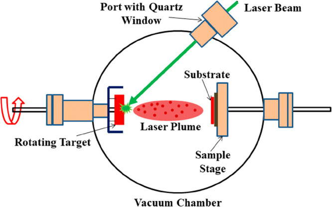
Diagram of a pulse laser deposition setup. Reprinted with permission from Soonmin et al.144 Copyright 2018 Mediterranean Journal of Chemistry.
Table 5. Literature Review for Pulsed Laser Deposition Techniques.
| Physical
parameters |
|||||||||||||
|---|---|---|---|---|---|---|---|---|---|---|---|---|---|
| Material | Temperature | Pressure | Crystal structure | Morphology | Configuration | Electrolyte | Type | PW | SC | ED | PD | Capacitive retention @ cycles | Ref |
| Mn2O3 @ Co3O4 | 3 × 10⁻⁷ Torr | Amorphous | Needle like | Liquid state (3 electrodes) | 0.1 M Na2SO4 | –0.1 to 0.9 | 99 F/g @ 5 mV/s | (152) | |||||
| Mn2O3 @ Mn3O4 | 3 × 10⁻⁷ Torr | Crystalline (Mn2O3); amorphous (Mn3O4) | Rough grain | Liquid state (3 electrodes) | 0.1 M Na2SO4 | –0.1 to 0.9 | 210 F/g @ 1 mV/s | (153) | |||||
| V–Mn2O3 @ Mn3O4 | 3 × 10⁻⁷ Torr | Amorphous | Grain | Liquid state (3 electrodes) | 0.5 M K2SO4 | –0.1 to 0.9 | 95 F/g @ 100 mV/s | (154) | |||||
| Al-CoOH/CoO | 10–4 Pa | Nanowalls | Liquid state (3 electrodes) | 3 M NaOH | 0 to 0.45 | 690 F/g @ 5 mV/s | (155) | ||||||
| Ni2Se/CNT | Amorphous | Shell | Liquid state (2 electrodes) | 1 M KOH | Asymmetric (CC@CNTs @NiSe //CC@CNTs) | 0 to 0.5 | 50.7 F/g @ 1 A/g | 11.9 Wh/kg | 242 W/kg | 85.5% @ 4000 | (101) | ||
| ZnO/carbon | 10–2 mbar | Wurtzite | Nanowall core–shell | Liquid state (3 electrodes) | 1 M KCl | 0 to 0.7 | 4.3 mF/cm2 @ 0.2 mA/cm2 | (147) | |||||
| WO3/V2O5 | 5 × 10⁻⁶ mbar | V2O5, orthorhombic; WO3, hexagonal | Hexagonal particles | Solid state | PVA-KOH | Asymmetric | 0 to 1.5 | 40.28 F/cm3 @ 0.1 mA/cm2 | 12.58 mWh/cm3 | 0.316 W/cm3 | 99.4% @ 50000 | (151) | |
| MnO2 | 300 °C | Crystalline | Foam like | Liquid state (3 electrodes) | 1 M Na2SO4 | 0 to 1.0 | 1000 F/g @ 5 mV/s | (146) | |||||
| CoFe2O4 | 450 °C | Amorphous | Liquid state (3 electrodes) | 1 M KOH | 0 to 0.5 | 777 F/g @ 0.5 mA/cm2 | 17.00 Wh/kg | 3.277 kW/kg | (148) | ||||
| Li2TiO3 | 600 °C | 0.4 mPa | Crystalline | Pyramidal nanoclusters | Liquid state (3 electrodes) | 1 M Li2SO4 | 0.0 to 1.0 | 283 mF/cm2@ 1 mA/cm2 | 94% @ 1000 | (149) | |||
| Ti3O5/CNT | 10–4 Pa | Amorphous | Core–shell | Liquid state (3 electrodes) | 1 M Na2SO4 | 0.0 to 0.7 | 445.7 F/g @ 1 A/g | 97% @ 3000 | (150) | ||||
Filters are employed to prevent material droplets from reaching the substrate, ensuring the quality of the thin film being deposited. These filters prevent droplets from polluting the final product by trapping them in a mesh or similar structure. PLD offers several additional appealing characteristics. It offers superior in situ temperature control as well as variable ablation rates for creating diverse micro/nanostructured films. Its ability to generate various morphologies is a critical requirement that determines the electrochemical performance of supercapacitors.145 The PLD technique is a very accurate and controlled approach for producing thin material layers. It is especially effective for forming a thin film of substances that are challenging to manufacture using other procedures, such as high-temperature or high-pressure procedures. It may also be utilized to produce films with exact thickness, content, and crystallographic orientation. Thin films are necessary for the manufacture of devices and sensors in sectors such as microelectronics, photonics, and biomedical engineering.
PLD is an advanced technique which can be used to form various morphologies of various materials to produce electrodes with superior electrochemical performance. A high specific capacitance of 1000 F/g with a potential window of 1 V was achieved by Lacerda et al.146 using manganese oxide nanofoam by employing PLD. Nonhomogeneous topography with microstructure was observed in FESEM images (Figure 39a and b). It helps in the transfer of electrolytes into pores and valleys of the material resulting in better electrochemical activities. TEM images showed amorphous contrast in some regions and concentric rings indicating crystalline property and strong reflection arc due to texturing particles (Figure 39c and d). TEM confirmed the presence of fine cluster grains.146
Figure 39.

(a),(b) SEM images and (c),(d) TEM images of manganese oxide nanofoam. Reprinted with permission from Lacerda et al.146 Copyright 2020 ELSEVIER Materials Chemistry and Physics.
It is obvious that the higher-temperature deposition results in the densification of the film and reduction in the surface porosity. Lacerda et al.146 studied the effect of deposition temperature on MnO2 deposited for supercapacitor applications. Figure 40a, b, and c shows the CV plots of MnO2 deposited at 300, 400, and 500 °C, respectively. From Figure 40d it is evident that with an increase in temperature the specific capacitance was reduced. The film deposited at 300 °C showed a higher capacitance of 1000 F/g at 5 mV/s scan rate than the film deposited at higher temperatures of 400 and 500 °C.146 Guerra et al.147 prepared a ZnO/carbon nanowall core–shell nanocomposite for supercapacitor applications. It exhibited a specific capacitance of 4.3 mF/cm2 at 0.2 mA/cm2 in a potential window from 0 to 0.7 V.147 CoFe2O4 bimetal oxide was synthesized by Nikam et al.,148 which showed good specific capacitance of 777 F/g at 0.5 mA/cm2 current density in 1 M KOH electrolyte. Li2TiO3 with pyramid nanoclusters surrounded by spherical-shaped grain morphology was deposited by Lakshmi-Narayana et al.149 It exhibited pseudocapacitive characteristics with 283 mF/cm2specific capacitance at a current density of 1 mA/cm2 along with cyclic stability of 94% over 1000 cycles.149 Sun et al.150 synthesized Ti3O5 on CNTs for supercapacitor applications. The core–shell nanocomposite showed specific capacitance of 445.7 F/g at 1 A/g with good capacitive retention of 97% after 3000 cycles.150
Figure 40.

Cyclic voltammetry with varying scan rates of a manganese oxide nanofoam heat-treated at (a) 300 °C, (b) 400 °C, (c) 500 °C, and (d) the corresponding specific capacitance for the three samples. Reprinted with permission from Lacerda et al.146 Copyright 2020 ELSEVIER Materials Chemistry and Physics.
Velmurugan et al.151 created thin-film supercapacitors made of tungsten trioxide and vanadium pentoxide (WO3 || V2O5). At 0.1 mA/cm2, the formed solid-state hybrid device had a potential of 1.5 V and a maximum specific volumetric capacitance of 40.28 F/cm3. A specific energy density of 12.6 mWh/cm3 was also obtained, along with a specific power density of 0.31 W/cm3. Furthermore, even after 50000 cycles, the device maintained an excellent efficiency of 99.4% and capacitance retention of 95.2%. Figure 41a, b, and c shows an as-fabricated device and the charging and discharging mechanism of the device, respectively. Dongfang Yang152−154 studied manganese oxide and its composite deposited through pulsed laser deposition for supercapacitor application. The Mn2O3@Co3O4152 composite with needle like morphology exhibited a specific capacitance of 99 F/g at 5 mV/s, whereas Mn2O3@Mn3O4153 exhibited a specific capacitance of 210 F/g at 1 mV/s due to its rough surface morphology. Vanadium-doped Mn2O3@Mn3O4154 showed excellent specific capacitance of 95 F/g at a higher scan rate of 100 mV/s.
Figure 41.

Figure representing the charge storage mechanism of an (a) as-fabricated cell; (b) charge state; (c) discharge condition; and (d) hybrid device manufacturing.151 Reprinted with permission from Velmurugan et al.151 Copyright 2020 Royal Society of Chemistry Journal of Material Chemistry A.
Various strategies have been employed by researchers to form highly porous electrodes which can show superior electrochemical properties. One such example is the film produced by Wang et al.155 where they formed aluminum-doped cobalt oxide thin film using PLD in an O2/H2 atmosphere. Then they etched the films using NaOH to remove aluminum oxide. The etching resulted in the formation of a cobalt oxide/hydroxide nanowall array film. The FESEM images of the film before and after the etching are shown in Figure 42a and b. The formation of a nanowall array is clearly visible after film etching, which created a great difference in the cyclic voltammogram (Figure 42c). The maximum obtained specific capacitance was 690 F/g at 5 mV/s.155
Figure 42.

(a) SEM images of aluminum-doped cobalt oxide and (b) SEM images of a cobalt oxide/hydroxide nanowall array film after NaOH etching. (c) The positive effect of etching on the film results in an increase in the area of the cyclic voltammogram of the film. Reprinted with permission from Wang et al.155 Copyright 2013 ELSEVIER Electrochemical Acta.
The pulsed laser deposition or ablation process holds the potential for future study of supercapacitor production employing a variety of materials on diverse substrates. This is a future technology that is most efficient in the deposition of films with varying physical properties that are optimized by adjusting deposition conditions. Asymmetric supercapacitor devices are becoming popular in the current era because they take advantage of two different active material electrodes. Nie et al.101 prepared NiSe2 over CC@CNT through PLD, where NiSe2 distributed over the CNT and strongly adhered to the CNT, thereby shortening the electron pathway resulting in good electrochemical behavior. Further they fabricated asymmetric CC@CNT//NiSe2@CNT@CC which achieved a specific capacitance of 50.77 F/g at a 1 A/g current density with 85% cyclic stability over 4000 cycles. It showed an energy and power density of 11.9 Wh/kg and 242 W/kg, respectively.101
10. Advantages and Disadvantages of Materials Deposited through Vacuum-Assisted Physical Deposition Techniques toward Supercapacitive Electrodes
10.1. Advantages
-
1.
Adhesion: Vacuum-assisted thin-film techniques provide excellent adhesion compared to chemical techniques.
-
2.
Large surface coating: These techniques are capable of large surface coating quickly and effectively and thus can be used in an industrial setting.
-
3.
In-situ thickness control: In-situ thickness control is possible by physical techniques by various sensors and detectors. These enable precise control over the thickness, material composition, and structure of deposited films, allowing for a wider range of particle size distribution and the creation of high-quality thin films with precise features and characteristics.156
-
4.
Repeatability: These procedures are extremely repeatable. This is crucial for mass production applications that demand a high degree of regularity.
-
5.
Environment friendly: Zero emission of toxic byproducts in the environment at the time of deposition, thus these processes are a low-toxic and environmentally favorable method for the creation of supercapacitor materials.157
-
6.
Directional deposition: Vacuum-assisted thin-film techniques are able to deposit highly directional films which is excellent to produce electrodes for microsupercapacitors using various masking techniques.
-
7.
Low substrate temperature: Deposition at a lower substrate temperature is possible; due to this a variety of temperature-sensitive material substrates may be used.158
-
8.
In-situ substrate cleaning: In the case of sputtering, in-situ cleaning of the substrate is possible by altering the voltage polarity between the target and substrate to improve the purity of the deposited film.159
-
9.
Low gaseous contamination: Gaseous contamination in the created films is limited due to the presence of a vacuum environment in a deposition chamber, and this results in the excellent purity of the product material film.160
10.2. Disadvantages
-
1.
Low porosity: One of the prime disadvantages of physical methods is that they produce highly uniform films with very low porosity. The low porosity of the film severely affects the electrochemical properties of the film.
-
2.
Cost of equipment: Small-scale enterprises may find it challenging to adopt vacuum deposition because the equipment is costly and may require specialized training to operate.
-
3.
Complex process: Vacuum deposition is a complicated process that necessitates careful monitoring of a number of variables, including temperature and pressure. As a result, manufacturing time and costs may increase.
-
4.
High energy use: Vacuum deposition can consume a lot of energy, which might increase production costs and raise environmental issues.
-
5.
Availability of source materials: Physical methods need high-purity source materials which are not available for all types of materials.
11. Conclusions
Supercapacitors are gaining attraction as a potential technology in a variety of sectors. Supercapacitors have various benefits over traditional electrochemical energy storage devices, including high power density, quick charge–discharge rates, extended cycle life, and environmental friendliness. As a result, researchers are increasingly driven to study supercapacitors in order to realize their full potential. Great efforts have been made in recent years to improve the energy density and power density of supercapacitors. These advancements have been made possible by enhancing the porosity, surface morphology, and electrochemical characteristics of the manufactured materials and thin films. The use of nanomaterials and hybrid composites has also been investigated in order to increase the specific surface area of supercapacitors and improve their electrochemical performance.
Moreover, portable, flexible, and solid-state microsupercapacitors have received a lot of interest recently. These devices are compact in size and may be incorporated into a variety of applications, including wearable electronics, Internet of Things (IoT) devices, and biomedical implants. These devices must be developed with care, taking into account variables like energy density, power density, mechanical flexibility, and stability. Advances in solid-state microsupercapacitor manufacturing show great potential for altering the energy storage landscape in the near future.
Vacuum-assisted thin-film techniques have been demonstrated to be extremely successful in the fabrication of microsupercapacitors. The extremely directed deposition procedure of this approach allows for the creation of highly accurate microelectrodes for microsupercapacitors. Other deposition procedures, including solution- and chemical-based approaches, are difficult to attain this level of accuracy, resulting in uneven and poorly defined electrode architectures. Furthermore, vacuum-assisted thin-film techniques have been effective in the production of completely functioning all-solid supercapacitor devices. This is due to the fact that the thickness and homogeneity of the deposited layers are precisely controlled, resulting in a high level of consistency and dependability in the final devices. Furthermore, vacuum-assisted thin-film techniques are relatively simple to implement and are compatible with various materials.
Despite the fact that vacuum-assisted thin-film techniques are extremely successful for the fabrication of microsupercapacitors, there is a remarkable scarcity of academic articles on the use of these techniques. This information gap gives a tremendous opportunity for academics and researchers to further examine these techniques in order to fully realize their potential. Nonetheless, it is critical to recognize that these strategies have some limits. One of the key disadvantages is that they produce films with low porosity and roughness, which can have a negative influence on the performance of the resulting supercapacitors. More exploration is required to tune the deposition parameters to overcome the constraints associated with these approaches.
Presently, the production of ultracapacitor electrodes employing these techniques is in its early stages, and a more detailed investigation of the factors that might affect the performance of supercapacitors fabricated using vacuum-assisted thin-film techniques is required. This article offers an overview of the present state of the design, fabrication, and assessment of supercapacitors using physical vapor deposition (PVD) processes, as well as outlines the key problems and future developments in this domain. As the number of practical applications for microsupercapacitors grows, so will the demand for novel production processes. This increased interest in microsupercapacitors will undoubtedly draw more researchers in the future, and we urge them to focus on overcoming issues related to the improvement of vacuum-assisted thin-film techniques. However, further study and improvement are required to fully realize their potential and overcome the limitations connected with these techniques.
12. Future Scope
-
1.
Supercapacitors provide several benefits, including fast charging and discharging, high power supply, exceptional cycle performance, and chemical stability. Supercapacitors are a wonderful option for energy storage devices because of these benefits; thus researchers should thoroughly investigate them.
-
2.
Liquid electrolyte-based supercapacitors have some disadvantages, including the potential for leakage and the difficulty in miniaturizing energy storage devices. With the ongoing miniaturization of electronics and gadgets, there is a growing demand for solid-state supercapacitors.
-
3.
Lightweight and compact microsupercapacitors are becoming increasingly popular in modern technological applications. Versatile microsupercapacitor devices are good candidates for the needed range of portable electronics applications.
-
4.
There is a critical need for research on solid-state microsupercapacitors since they could address numerous power storage industry issues.
-
5.
Physical deposition techniques tend to be a very efficient way to make microsupercapacitors. They offer more accurate directional film deposition than solution-based techniques using a variety of masking techniques.
-
6.
A variety of materials can be deposited using vacuum-assisted thin-film processes on a broad range of substrate types. These techniques offer precise film composition and thickness control by altering deposition parameters. Researchers are getting interested in these benefits.
-
7.
These processes produce very homogeneous, less porous films, which are their main drawbacks. The performance of supercapacitors may suffer as a result. To improve performance, various parameters of film formation need to be adjusted to achieve superior morphologies.
-
8.
The effect of adhesion using different substrates which in turn affects the supercapacitive properties of thin films needs to be studied.
-
9.
Many materials like metal alloys, metal chalcogenides, chalcopyrites, metals and metal phosphates, and their composites with other pseudocapacitive and EDLC materials need to explore which will have a high impact toward technological advancement in supercapacitors from micro- to macroscale devices limited to not only liquid-based but also the solid-state.
13. Challenges to Explore toward Supercapacitive Applications
-
1.
To explore vacuum techniques to get very high surface area nanomaterials with nanoporosity.
-
2.
To maintain good stoichiometry from the top to bottom of the thin-film material.
-
3.
To coat high surface area nanotubes/nanowires/nanorods with other materials, covering the entire surface is difficult.
-
4.
Filling the porous area from top to bottom is quite difficult without forming a shadow.
-
5.
Different forms of nanomaterials like quantum dots (Q-dots), nanorods, nanobeads, nanowires, and nanotubes with precise control are difficult to form.
Acknowledgments
B.R.S. acknowledges Director, VNIT, Nagpur. T.K.S. is thankful to DST (DST/INSPIRE/03/2022/000141) for providing an INSPIRE fellowship.
The authors declare no competing financial interest.
References
- Wayu M. Manganese Oxide Carbon-Based Nanocomposite in Energy Storage Applications. Solids 2021, 2 (2), 232–248. 10.3390/solids2020015. [DOI] [Google Scholar]
- Mathis T. S.; Kurra N.; Wang X.; Pinto D.; Simon P.; Gogotsi Y. Energy Storage Data Reporting in Perspective—Guidelines for Interpreting the Performance of Electrochemical Energy Storage Systems. Adv. Energy Mater. 2019, 9 (39), 1–13. 10.1002/aenm.201902007. [DOI] [Google Scholar]
- Liu Y.; Wu Q.; Liu L.; Manasa P.; Kang L.; Ran F. Vanadium Nitride for Aqueous Supercapacitors: A Topic Review. J. Mater. Chem. A 2020, 8 (17), 8218–8233. 10.1039/D0TA01490G. [DOI] [Google Scholar]
- Becker H. J.Low Voltage Electrolytic Capacitor, April 14, 1954.
- Pande S. A.; Pandit B.; Sankapal B. R. Facile Chemical Route for Multiwalled Carbon Nanotube/Mercury Sulfide Nanocomposite: High Performance Supercapacitive Electrode. J. Colloid Interface Sci. 2018, 514, 740–749. 10.1016/j.jcis.2017.12.068. [DOI] [PubMed] [Google Scholar]
- Sankapal B. R.; Gajare H. B.; Karade S. S.; Dubal D. P. Anchoring Cobalt Oxide Nanoparticles on to the Surface Multiwalled Carbon Nanotubes for Improved Supercapacitive Performances. RSC Adv. 2015, 5 (60), 48426–48432. 10.1039/C5RA06377A. [DOI] [Google Scholar]
- Ray A.; Korkut D.; Saruhan B. Efficient Flexible All-Solid Supercapacitors with Direct Sputter-Grown Needle-like Mn/MnOx @graphite-Foil Electrodes and Ppc-Embedded Ionic Electrolytes. Nanomaterials 2020, 10 (9), 1768. 10.3390/nano10091768. [DOI] [PMC free article] [PubMed] [Google Scholar]
- Karade S. S.; Dubal D. P.; Sankapal B. R. Decoration of Ultrathin MoS2 Nanoflakes over MWCNTs: Enhanced Supercapacitive Performance through Electrode to Symmetric All-Solid-State Device. ChemistrySelect 2017, 2 (32), 10405–10412. 10.1002/slct.201701788. [DOI] [Google Scholar]
- Li X.; Zhao T.; Chen Q.; Li P.; Wang K.; Zhong M.; Wei J.; Wu D.; Wei B.; Zhu H. Flexible All Solid-State Supercapacitors Based on Chemical Vapor Deposition Derived Graphene Fibers. Phys. Chem. Chem. Phys. 2013, 15 (41), 17752–17757. 10.1039/c3cp52908h. [DOI] [PubMed] [Google Scholar]
- Gao Z.; Wu Z.; Zhao S.; Zhang T.; Wang Q. Enhanced Capacitive Property of HfN Film Electrode by Plasma Etching for Supercapacitors. Mater. Lett. 2019, 235, 148–152. 10.1016/j.matlet.2018.10.032. [DOI] [Google Scholar]
- Liu Y.; Xu N.; Chen W.; Wang X.; Sun C.; Su Z. Supercapacitor with High Cycling Stability through Electrochemical Deposition of Metal–Organic Frameworks/Polypyrrole Positive Electrode. Dalt. Trans. 2018, 47 (38), 13472–13478. 10.1039/C8DT02740D. [DOI] [PubMed] [Google Scholar]
- Pande S. A.; Pandit B.; Sankapal B. R. Vanadium Oxide Anchored MWCNTs Nanostructure for Superior Symmetric Electrochemical Supercapacitors. Mater. Des. 2019, 182, 107972 10.1016/j.matdes.2019.107972. [DOI] [Google Scholar]
- Karade S. S.; Sankapal B. R. Materials Mutualism through EDLC-Behaved MWCNTs with Pseudocapacitive MoTe2 Nanopebbles: Enhanced Supercapacitive Performance. ACS Sustain. Chem. Eng. 2018, 6 (11), 15072–15082. 10.1021/acssuschemeng.8b03366. [DOI] [Google Scholar]
- Varshney B.; Siddiqui M. J.; Anwer A. H.; Khan M. Z.; Ahmed F.; Aljaafari A.; Hammud H. H.; Azam A. Synthesis of Mesoporous SnO2/NiO Nanocomposite Using Modified Sol–Gel Method and Its Electrochemical Performance as Electrode Material for Supercapacitors. Sci. Reports 2020 101 2020, 10 (1), 1–13. 10.1038/s41598-020-67990-8. [DOI] [PMC free article] [PubMed] [Google Scholar]
- Garakani M. A.; Bellani S.; Pellegrini V.; Oropesa-Nuñez R.; Castillo A. E. D. R.; Abouali S.; Najafi L.; Martín-García B.; Ansaldo A.; Bondavalli P.; Demirci C.; Romano V.; Mantero E.; Marasco L.; Prato M.; Bracciale G.; Bonaccorso F. Scalable Spray-Coated Graphene-Based Electrodes for High-Power Electrochemical Double-Layer Capacitors Operating over a Wide Range of Temperature. Energy Storage Mater. 2021, 34, 1–11. 10.1016/j.ensm.2020.08.036. [DOI] [Google Scholar]
- Lai L.; Clark M.; Su S.; Li R.; Ivey D. G.; Zhu X. Dip-Coating Synthesis of RGO/α-Ni(OH)2@nickel Foam with Layer-by-Layer Structure for High Performance Binder-Free Supercapacitors. Electrochim. Acta 2021, 368, 137589 10.1016/j.electacta.2020.137589. [DOI] [Google Scholar]
- Pandit B.; Sankapal B. R. Highly Conductive Energy Efficient Electroless Anchored Silver Nanoparticles on MWCNTs as a Supercapacitive Electrode. New J. Chem. 2017, 41 (19), 10808–10814. 10.1039/C7NJ01792H. [DOI] [Google Scholar]
- Nikam S. M.; Sharma A.; Rahaman M.; Teli A. M.; Mujawar S. H.; Zahn D. R. T.; Patil P. S.; Sahoo S. C.; Salvan G.; Patil P. B. Pulsed Laser Deposited CoFe2O4 Thin Films as Supercapacitor Electrodes. RSC Adv. 2020, 10 (33), 19353–19359. 10.1039/D0RA02564J. [DOI] [PMC free article] [PubMed] [Google Scholar]
- Kiamahalleh M. V.; Zein S. H. S.; Najafpour G.; Sata S. A.; Buniran S. Multiwalled Carbon Nanotubes Based Nanocomposites for Supercapacitors: A Review of Electrode Materials. Nano 2012, 10.1142/S1793292012300022. [DOI] [Google Scholar]
- Conway B. E. Transition from “supercapacitor” to “Battery” Behavior in Electrochemical Energy Storage. Proc. Int. Power Sources Symp. 1991, 138 (6), 319–327. 10.1149/1.2085829/XML. [DOI] [Google Scholar]
- Nair N.; Sankapal B. R.. Chemically Deposited Metal Chalcogenide-Based Carbon Composites for Versatile Applications; Ezema F., Lokhande C., Lokhande A., Eds.; Springer, 2023. [Google Scholar]
- González A.; Goikolea E.; Barrena J. A.; Mysyk R. Review on Supercapacitors: Technologies and Materials. Renew. Sustain. Energy Rev. 2016, 58, 1189–1206. 10.1016/j.rser.2015.12.249. [DOI] [Google Scholar]
- Iro Z. S.; Subramani C.; Dash S. S. A Brief Review on Electrode Materials for Supercapacitor. Int. J. Electrochem. Sci. 2016, 11 (12), 10628–10643. 10.20964/2016.12.50. [DOI] [Google Scholar]
- Simon P.; Gogotsi Y.. Materials for Electrochemical Capacitors. Nat. Mater.; Nature Publishing Group, 2008; pp 845–854. 10.1038/nmat2297. [DOI] [PubMed] [Google Scholar]
- Conway B. E. Electrochemical Supercapacitors. Electrochem. Supercapacitors 1999, 10.1007/978-1-4757-3058-6. [DOI] [Google Scholar]
- Zhang Y.; Feng H.; Wu X.; Wang L.; Zhang A.; Xia T.; Dong H.; Li X.; Zhang L. Progress of Electrochemical Capacitor Electrode Materials: A Review. Int. J. Hydrogen Energy 2009, 34 (11), 4889–4899. 10.1016/j.ijhydene.2009.04.005. [DOI] [Google Scholar]
- Shukla A. K.; Sampath S.; Vijayamohanan K. Electrochemical Supercapacitors: Energy Storage beyond Batteries. Current Science 2000, 1656–1661. [Google Scholar]
- Shao Y.; El-Kady M. F.; Sun J.; Li Y.; Zhang Q.; Zhu M.; Wang H.; Dunn B.; Kaner R. B. Design and Mechanisms of Asymmetric Supercapacitors. Chem. Rev. 2018, 118 (18), 9233–9280. 10.1021/acs.chemrev.8b00252. [DOI] [PubMed] [Google Scholar]
- Lim E.; Jo C.; Lee J. A Mini Review of Designed Mesoporous Materials for Energy-Storage Applications: From Electric Double-Layer Capacitors to Hybrid Supercapacitors. Nanoscale 2016, 8 (15), 7827–7833. 10.1039/C6NR00796A. [DOI] [PubMed] [Google Scholar]
- Ding J.; Hu W.; Paek E.; Mitlin D. Review of Hybrid Ion Capacitors: From Aqueous to Lithium to Sodium. Chem. Rev. 2018, 118 (14), 6457–6498. 10.1021/acs.chemrev.8b00116. [DOI] [PubMed] [Google Scholar]
- Coleman J. N.; Khan U.; Blau W. J.; Gun’ko Y. K. Small but Strong: A Review of the Mechanical Properties of Carbon Nanotube–Polymer Composites. Carbon N. Y. 2006, 44 (9), 1624–1652. 10.1016/j.carbon.2006.02.038. [DOI] [Google Scholar]
- Xu Y.; Lu W.; Xu G.; Chou T. W. Structural Supercapacitor Composites: A Review. Compos. Sci. Technol. 2021, 204, 108636 10.1016/j.compscitech.2020.108636. [DOI] [Google Scholar]
- Pandit B.; Rondiya S. R.; Cross R. W.; Dzade N. Y.; Sankapal B. R. Vanadium Telluride Nanoparticles on MWCNTs Prepared by Successive Ionic Layer Adsorption and Reaction for Solid-State Supercapacitor. Chem. Eng. J. 2022, 429, 132505 10.1016/j.cej.2021.132505. [DOI] [Google Scholar]
- Najib S.; Erdem E. Current Progress Achieved in Novel Materials for Supercapacitor Electrodes: Mini Review. Nanoscale Adv. 2019, 1 (8), 2817–2827. 10.1039/C9NA00345B. [DOI] [PMC free article] [PubMed] [Google Scholar]
- Elgrishi N.; Rountree K. J.; McCarthy B. D.; Rountree E. S.; Eisenhart T. T.; Dempsey J. L. A Practical Beginner’s Guide to Cyclic Voltammetry. J. Chem. Educ. 2018, 95 (2), 197–206. 10.1021/acs.jchemed.7b00361. [DOI] [Google Scholar]
- Chodankar N. R.; Pham H. D.; Nanjundan A. K.; Fernando J. F. S.; Jayaramulu K.; Golberg D.; Han Y. K.; Dubal D. P. True Meaning of Pseudocapacitors and Their Performance Metrics: Asymmetric versus Hybrid Supercapacitors. Small 2020, 16 (37), 1–35. 10.1002/smll.202002806. [DOI] [PubMed] [Google Scholar]
- Gogotsi Y.; Penner R. M. Energy Storage in Nanomaterials - Capacitive, Pseudocapacitive, or Battery-Like?. ACS Nano 2018, 12 (3), 2081–2083. 10.1021/acsnano.8b01914. [DOI] [PubMed] [Google Scholar]
- Huang J.; Yuan K.; Chen Y. Wide Voltage Aqueous Asymmetric Supercapacitors: Advances, Strategies, and Challenges. Adv. Funct. Mater. 2022, 32 (4), 2108107 10.1002/adfm.202108107. [DOI] [Google Scholar]
- Agarwal A.; Sankapal B. R. Metal Phosphides: Topical Advances in the Design of Supercapacitors. J. Mater. Chem. A 2021, 9 (36), 20241–20276. 10.1039/D1TA04104E. [DOI] [Google Scholar]
- Lazanas A. C.; Prodromidis M. I. Electrochemical Impedance Spectroscopy—A Tutorial. ACS Meas. Sci. Au 2023, 3, 162. 10.1021/acsmeasuresciau.2c00070. [DOI] [PMC free article] [PubMed] [Google Scholar]
- Mei B. A.; Munteshari O.; Lau J.; Dunn B.; Pilon L. Physical Interpretations of Nyquist Plots for EDLC Electrodes and Devices. J. Phys. Chem. C 2018, 122 (1), 194–206. 10.1021/acs.jpcc.7b10582. [DOI] [Google Scholar]
- Kouchachvili L.; Yaïci W.; Entchev E. Hybrid Battery/Supercapacitor Energy Storage System for the Electric Vehicles. J. Power Sources 2018, 374, 237–248. 10.1016/j.jpowsour.2017.11.040. [DOI] [Google Scholar]
- Agarwal A.; Sankapal B. R. Ultrathin Cu2P2O7 Nanoflakes on Stainless Steel Substrate for Flexible Symmetric All-Solid-State Supercapacitors. Chem. Eng. J. 2021, 422, 130131 10.1016/j.cej.2021.130131. [DOI] [Google Scholar]
- Zhou Y.; Lachman N.; Ghaffari M.; Xu H.; Bhattacharya D.; Fattahi P.; Abidian M. R.; Wu S.; Gleason K. K.; Wardle B. L.; Zhang Q. M. A High Performance Hybrid Asymmetric Supercapacitor via Nano-Scale Morphology Control of Graphene, Conducting Polymer, and Carbon Nanotube Electrodes. J. Mater. Chem. A 2014, 2 (26), 9964–9969. 10.1039/C4TA01785D. [DOI] [Google Scholar]
- Yan J.; Wang Q.; Wei T.; Fan Z. Recent Advances in Design and Fabrication of Electrochemical Supercapacitors with High Energy Densities. Adv. Energy Mater. 2014, 4 (4), 1300816. 10.1002/aenm.201300816. [DOI] [Google Scholar]
- Lim J. M.; Jang Y. S.; Van T.; Nguyen H.; Kim J. S.; Yoon Y.; Park B. J.; Seo D. H.; Lee K. K.; Han Z.; Ostrikov K.; Doo S. G. Advances in High-Voltage Supercapacitors for Energy Storage Systems: Materials and Electrolyte Tailoring to Implementation. Nanoscale Adv. 2023, 5 (3), 615–626. 10.1039/D2NA00863G. [DOI] [PMC free article] [PubMed] [Google Scholar]
- Liu C.; Yan X.; Hu F.; Gao G.; Wu G.; Yang X. Toward Superior Capacitive Energy Storage: Recent Advances in Pore Engineering for Dense Electrodes. Adv. Mater. 2018, 30 (17), 1–14. 10.1002/adma.201705713. [DOI] [PubMed] [Google Scholar]
- Deshmukh T. B.; Babar P.; Kedara Shivasharma T.; Sankapal B. R. Mixed-Valence Iron Phosphate: Superhydrophilic Multi-Plated Microflakes towards Symmetric Supercapacitor. Surfaces and Interfaces 2022, 35, 102419 10.1016/j.surfin.2022.102419. [DOI] [Google Scholar]
- Zhang L.; Yang S.; Chang J.; Zhao D.; Wang J.; Yang C.; Cao B. A Review of Redox Electrolytes for Supercapacitors. Front. Chem. 2020, 8 (June), 1–7. 10.3389/fchem.2020.00413. [DOI] [PMC free article] [PubMed] [Google Scholar]
- Pandit B.; Devika V. S.; Sankapal B. R. Electroless-Deposited Ag Nanoparticles for Highly Stable Energy-Efficient Electrochemical Supercapacitor. J. Alloys Compd. 2017, 726, 1295–1303. 10.1016/j.jallcom.2017.08.068. [DOI] [Google Scholar]
- Pal B.; Yang S.; Ramesh S.; Thangadurai V.; Jose R. Electrolyte Selection for Supercapacitive Devices: A Critical Review. Nanoscale Adv. 2019, 1 (10), 3807–3835. 10.1039/C9NA00374F. [DOI] [PMC free article] [PubMed] [Google Scholar]
- Raza W.; Ali F.; Raza N.; Luo Y.; Kim K. H.; Yang J.; Kumar S.; Mehmood A.; Kwon E. E. Recent Advancements in Supercapacitor Technology. Nano Energy 2018, 52 (July), 441–473. 10.1016/j.nanoen.2018.08.013. [DOI] [Google Scholar]
- Zhai S.; Chen Y. Graphene-Based Fiber Supercapacitors. Accounts Mater. Res. 2022, 3 (9), 922–934. 10.1021/accountsmr.2c00087. [DOI] [Google Scholar]
- Tong L.; Gao M.; Jiang C.; Cai K. Ultra-High Performance and Flexible Polypyrrole Coated CNT Paper Electrodes for All-Solid-State Supercapacitors. J. Mater. Chem. A 2019, 7 (17), 10751–10760. 10.1039/C9TA01856E. [DOI] [Google Scholar]
- Raymundo-Piñero E.; Leroux F.; Béguin F. A High-Performance Carbon for Supercapacitors Obtained by Carbonization of a Seaweed Biopolymer. Adv. Mater. 2006, 18 (14), 1877–1882. 10.1002/adma.200501905. [DOI] [Google Scholar]
- Majumdar D.; Maiyalagan T.; Jiang Z. Recent Progress in Ruthenium Oxide-Based Composites for Supercapacitor Applications. ChemElectroChem. 2019, 6 (17), 4343–4372. 10.1002/celc.201900668. [DOI] [Google Scholar]
- Dhas S. D.; Maldar P. S.; Patil M. D.; Nagare A. B.; Waikar M. R.; Sonkawade R. G.; Moholkar A. V. Synthesis of NiO Nanoparticles for Supercapacitor Application as an Efficient Electrode Material. Vacuum 2020, 181, 109646 10.1016/j.vacuum.2020.109646. [DOI] [Google Scholar]
- Yu J.; Li M.; Wang X.; Yang Z. Promising High-Performance Supercapacitor Electrode Materials from MnO2 Nanosheets@Bamboo Leaf Carbon. ACS Omega 2020, 5 (26), 16299–16306. 10.1021/acsomega.0c02169. [DOI] [PMC free article] [PubMed] [Google Scholar]
- Meher S. K.; Rao G. R. Ultralayered Co3O4 for High-Performance Supercapacitor Applications. J. Phys. Chem. C 2011, 115 (31), 15646–15654. 10.1021/jp201200e. [DOI] [Google Scholar]
- Balamuralitharan B.; Cho I. H.; Bak J. S.; Kim H. J. V2O5 Nanorod Electrode Material for Enhanced Electrochemical Properties by a Facile Hydrothermal Method for Supercapacitor Applications. New J. Chem. 2018, 42 (14), 11862–11868. 10.1039/C8NJ02377H. [DOI] [Google Scholar]
- Meng Q.; Cai K.; Chen Y.; Chen L. Research Progress on Conducting Polymer Based Supercapacitor Electrode Materials. Nano Energy 2017, 36, 268–285. 10.1016/j.nanoen.2017.04.040. [DOI] [Google Scholar]
- Sajjad M.; Cheng F.; Lu W. Research Progress in Transition Metal Chalcogenide Based Anodes for K-Ion Hybrid Capacitor Applications: A Mini-Review. RSC Adv. 2021, 11 (41), 25450–25460. 10.1039/D1RA02445K. [DOI] [PMC free article] [PubMed] [Google Scholar]
- Pandit B.; Karade S. S.; Sankapal B. R. Hexagonal VS2 Anchored MWCNTs: First Approach to Design Flexible Solid-State Symmetric Supercapacitor Device. ACS Appl. Mater. Interfaces 2017, 9 (51), 44880–44891. 10.1021/acsami.7b13908. [DOI] [PubMed] [Google Scholar]
- Hwang N. M.Non-Classical Crystallization of Thin Films and Nanostructures in CVD and PVD Processes; Springer, 2016. [Google Scholar]
- Ani M. H.; Kamarudin M. A.; Ramlan A. H.; Ismail E.; Sirat M. S.; Mohamed M. A.; Azam M. A. A Critical Review on the Contributions of Chemical and Physical Factors toward the Nucleation and Growth of Large-Area Graphene. J. Mater. Sci. 2018, 53 (10), 7095–7111. 10.1007/s10853-018-1994-0. [DOI] [Google Scholar]
- Greene J. E.Thin Film Nucleation, Growth, and Microstructural Evolution: An Atomic Scale View, 3rd ed.; Elsevier Ltd., 2009. 10.1016/B978-0-8155-2031-3.00012-0. [DOI] [Google Scholar]
- Thanh N. T. K.; Maclean N.; Mahiddine S. Mechanisms of Nucleation and Growth of Nanoparticles in Solution. Chem. Rev. 2014, 114 (15), 7610–7630. 10.1021/cr400544s. [DOI] [PubMed] [Google Scholar]
- Chopra K. L.Thin Film Phenomena; McGraw-Hill, 1969; pp 844. [Google Scholar]
- Wu K. J.; Tse E. C. M.; Shang C.; Guo Z. Nucleation and Growth in Solution Synthesis of Nanostructures – From Fundamentals to Advanced Applications. Prog. Mater. Sci. 2022, 123, 100821 10.1016/j.pmatsci.2021.100821. [DOI] [Google Scholar]
- Hamdallah S. I.; Zoqlam R.; Erfle P.; Blyth M.; Alkilany A. M.; Dietzel A.; Qi S. Microfluidics for Pharmaceutical Nanoparticle Fabrication: The Truth and the Myth. Int. J. Pharm. 2020, 584, 119408 10.1016/j.ijpharm.2020.119408. [DOI] [PubMed] [Google Scholar]
- Tour J. M. Top-down versus Bottom-up Fabrication of Graphene-Based Electronics. Chem. Mater. 2014, 26 (1), 163–171. 10.1021/cm402179h. [DOI] [Google Scholar]
- Teo B. K.; Sun X. H. From Top-down to Bottom-up to Hybrid Nanotechnologies: Road to Nanodevices. J. Clust. Sci. 2006, 17 (4), 529–540. 10.1007/s10876-006-0086-5. [DOI] [Google Scholar]
- Ochekpe N. A.; Olorunfemi P. O.; Ngwuluka N. C. Nanotechnology and Drug Delivery Part 2: Nanostructures for Drug Delivery. Trop. J. Pharm. Res. 2009, 8 (3), 275–287. 10.4314/tjpr.v8i3.44547. [DOI] [Google Scholar]
- Liu W. K.; Karpov E. G.; Zhang S.; Park H. S. An Introduction to Computational Nanomechanics and Materials. Comput. Methods Appl. Mech. Eng. 2004, 193 (17–20), 1529–1578. 10.1016/j.cma.2003.12.008. [DOI] [Google Scholar]
- Mendes P. M.; Jacke S.; Critchley K.; Plaza J.; Chen Y.; Nikitin K.; Palmer R. E.; Preece J. A.; Evans S. D.; Fitzmaurice D. Gold Nanoparticle Patterning of Silicon Wafers Using Chemical E-Beam Lithography. Langmuir 2004, 20 (9), 3766–3768. 10.1021/la049803g. [DOI] [PubMed] [Google Scholar]
- Smith R. K.; Lewis P. A.; Weiss P. S. Patterning Self-Assembled Monolayers. Prog. Surf. Sci. 2004, 75 (1–2), 1–68. 10.1016/j.progsurf.2003.12.001. [DOI] [Google Scholar]
- Imahori H.; Arimura M.; Hanada T.; Nishimura Y.; Yamazaki I.; Sakata Y.; Fukuzumi S. Photoactive Three-Dimensional Monolayers: Porphyrin - Alkanethiolate-Stabilized Gold Clusters. J. Am. Chem. Soc. 2001, 123 (2), 335–336. 10.1021/ja002838s. [DOI] [PubMed] [Google Scholar]
- Roth K. M.; Lindsey J. S.; Bocian D. F.; Kuhr W. G. Characterization of Charge Storage in Redox-Active Self-Assembled Monolayers. Langmuir 2002, 18 (10), 4030–4040. 10.1021/la025525e. [DOI] [Google Scholar]
- Pandit B.; Bommineedi L. K.; Sankapal B. R. Electrochemical Engineering Approach of High Performance Solid-State Flexible Supercapacitor Device Based on Chemically Synthesized VS2 Nanoregime Structure. J. Energy Chem. 2019, 31, 79–88. 10.1016/j.jechem.2018.05.011. [DOI] [Google Scholar]
- Baviskar P. K.; Nikam P. R.; Gargote S. S.; Ennaoui A.; Sankapal B. R. Controlled Synthesis of ZnO Nanostructures with Assorted Morphologies via Simple Solution Chemistry. J. Alloys Compd. 2013, 551, 233–242. 10.1016/j.jallcom.2012.10.052. [DOI] [Google Scholar]
- Arthur J. R. Physical and Chemical Methods for Thin-Film Deposition and Epitaxial Growth. Specim. Handl. Prep. Treat. Surf. Charact. 2002, 239–293. 10.1007/0-306-46913-8_8. [DOI] [Google Scholar]
- Salunkhe D. B.; Gargote S. S.; Dubal D. P.; Kim W. B.; Sankapal B. R. Sb2S3 Nanoparticles through Solution Chemistry on Mesoporous TiO2 for Solar Cell Application. Chem. Phys. Lett. 2012, 554, 150–154. 10.1016/j.cplett.2012.10.032. [DOI] [Google Scholar]
- Nikam P. R.; Baviskar P. K.; Sali J. V.; Gurav K. V.; Kim J. H.; Sankapal B. R. SILAR Coated Bi2S3 Nanoparticles on Vertically Aligned ZnO Nanorods: Synthesis and Characterizations. Ceram. Int. 2015, 41 (9), 10394–10399. 10.1016/j.ceramint.2015.03.239. [DOI] [Google Scholar]
- Sonawane N. B.; Gurav K. V.; Ahire R. R.; Kim J. H.; Sankapal B. R. CdS Nanowires with PbS Nanoparticles Surface Coating as Room Temperature Liquefied Petroleum Gas Sensor. Sensors Actuators A Phys. 2014, 216, 78–83. 10.1016/j.sna.2014.05.012. [DOI] [Google Scholar]
- Gomez J.; Kalu E. E. High-Performance Binder-Free Co–Mn Composite Oxide Supercapacitor Electrode. J. Power Sources 2013, 230, 218–224. 10.1016/j.jpowsour.2012.12.069. [DOI] [Google Scholar]
- Wang D.; Xie T.; Li Y. Nanocrystals: Solution-Based Synthesis and Applications as Nanocatalysts. Nano Res. 2009, 2 (1), 30–46. 10.1007/s12274-009-9007-x. [DOI] [Google Scholar]
- Devasia R.; Painuly A.; Devapal D.; Sreejith K. J. Continuous Fiber Reinforced Ceramic Matrix Composites. Fiber Reinf. Compos. Const. Compat. Perspect. Appl. 2021, 669–751. 10.1016/B978-0-12-821090-1.00022-3. [DOI] [Google Scholar]
- Youn W. K.; Lee S. S.; Lee J. Y.; Kim C. S.; Hwang N. M.; Iijima S. Comparison of the Deposition Behavior of Charged Silicon Nanoparticles between Floating and Grounded Substrates. J. Phys. Chem. C 2014, 118 (22), 11946–11953. 10.1021/jp5001144. [DOI] [Google Scholar]
- Kim D. Y.; Kwon J. H.; Jang G. S.; Hwang N. M. Effect of Pressure on the Film Deposition during Rf Magnetron Sputtering Considering Charged Nanoparticles. Coatings 2021, 11 (2), 132. 10.3390/coatings11020132. [DOI] [Google Scholar]
- Boeira C. D.; Leidens L. M.; Michels A. F.; Serra R.; Evaristo M.; Fernandes F.; Cavaleiro A.; Figueroa C. A. Influence of Base Pressure Prior to Deposition on the Adhesion Behaviour of Carbon Thin Films on Steel. Appl. Surf. Sci. Adv. 2020, 2, 100034 10.1016/j.apsadv.2020.100034. [DOI] [Google Scholar]
- Chandra G. H.; de la Cruz J. P.; Ventura J. The Influence of Argon Pressure and RF Power on the Growth of InP Thin Films. Semicond. Sci. Technol. 2011, 26 (7), 075017. 10.1088/0268-1242/26/7/075017. [DOI] [Google Scholar]
- Das N. K.; Chakrabartty J.; Farhad S. F. U.; Sen Gupta A. K.; Ikball Ahamed E. M. K.; Rahman K. S.; Wafi A.; Alkahtani A. A.; Matin M. A.; Amin N. Effect of Substrate Temperature on the Properties of RF Sputtered CdS Thin Films for Solar Cell Applications. Results Phys. 2020, 17, 103132. 10.1016/j.rinp.2020.103132. [DOI] [Google Scholar]
- Chen G.; Lu B.; Cui X.; Xiao J. Effects of Deposition and Annealing Temperature on the Structure and Optical Band Gap of MoS2 Films. Materials (Basel) 2020, 13 (23), 5515. 10.3390/ma13235515. [DOI] [PMC free article] [PubMed] [Google Scholar]
- Ghorannevis Z.; Hosseinnejad M. T.; Habibi M.; Golmahdi P. Effect of Substrate Temperature on Structural, Morphological and Optical Properties of Deposited Al/ZnO Films. J. Theor. Appl. Phys. 2015, 9 (1), 33–38. 10.1007/s40094-014-0157-1. [DOI] [Google Scholar]
- Mahdhi H.; Ben Ayadi Z.; Alaya S.; Gauffier J. L.; Djessas K. The Effects of Dopant Concentration and Deposition Temperature on the Structural, Optical and Electrical Properties of Ga-Doped ZnO Thin Films. Superlattices Microstruct. 2014, 72, 60–71. 10.1016/j.spmi.2014.04.013. [DOI] [Google Scholar]
- Mirabito T.; Huet B.; Redwing J. M.; Snyder D. W. Influence of the Underlying Substrate on the Physical Vapor Deposition of Zn-Phthalocyanine on Graphene. ACS Omega 2021, 6 (31), 20598–20610. 10.1021/acsomega.1c02758. [DOI] [PMC free article] [PubMed] [Google Scholar]
- Wang J.; Li F.; Zhu F.; Schmidt O. G. Recent Progress in Micro-Supercapacitor Design, Integration, and Functionalization. Small Methods 2019, 3 (8), 1–27. 10.1002/smtd.201800367. [DOI] [Google Scholar]
- Dubal D. P.; Chodankar N. R.; Kim D. H.; Gomez-Romero P. Towards Flexible Solid-State Supercapacitors for Smart and Wearable Electronics. Chem. Soc. Rev. 2018, 47 (6), 2065–2129. 10.1039/C7CS00505A. [DOI] [PubMed] [Google Scholar]
- Ma L.; Yang Y. Solid-State Supercapacitors for Electronic Device Applications. Appl. Phys. Lett. 2005, 87 (12), 1–3. 10.1063/1.2051797. [DOI] [Google Scholar]
- Ouendi S.; Robert K.; Stievenard D.; Brousse T.; Roussel P.; Lethien C. Sputtered Tungsten Nitride Films as Pseudocapacitive Electrode for on Chip Micro-Supercapacitors. Energy Storage Mater. 2019, 20 (April), 243–252. 10.1016/j.ensm.2019.04.006. [DOI] [Google Scholar]
- Nie R.; Wang Q.; Sun P.; Wang R.; Yuan Q.; Wang X. Pulsed Laser Deposition of NiSe2 Film on Carbon Nanotubes for High-Performance Supercapacitor. Eng. Sci. 2018, 6, 22–29. 10.30919/es8d668. [DOI] [Google Scholar]
- Qaid S. M. H.; Ghaithan H. M.; Al-Asbahi B. A.; Aldwayyan A. S. Single-Source Thermal Evaporation Growth and the Tuning Surface Passivation Layer Thickness Effect in Enhanced Amplified Spontaneous Emission Properties of CsPb(Br0.5Cl0.5)3 Perovskite Films. Polymers (Basel) 2020, 12 (12), 2953. 10.3390/polym12122953. [DOI] [PMC free article] [PubMed] [Google Scholar]
- Guru Prakash N.; Dhananjaya M.; Purusottam Reddy B.; Sivajee Ganesh K.; Lakshmi Narayana A.; Hussain O. M. Molybdenum Doped V2O5 Thin Films Electrodes for Supercapacitors. Mater. Today Proc. 2016, 3 (10), 4076–4081. 10.1016/j.matpr.2016.11.076. [DOI] [Google Scholar]
- Dhananjaya M.; Prakash N. G.; Sandhya G. L.; Narayana A. L.; Hussain O. M. Microstructure and Supercapacitor Properties of V2O5 Thin Film Prepared by Thermal Evaporation Method. Mater. Sci. Eng. 2017, 1–8. 10.2412/mmse.88.66.781. [DOI] [Google Scholar]
- Velmurugan R.; Premkumar J.; Pitchai R.; Ulaganathan M.; Subramanian B. Robust, Flexible, and Binder Free Highly Crystalline V2O5 Thin Film Electrodes and Their Superior Supercapacitor Performance. ACS Sustain. Chem. Eng. 2019, 7 (15), 13115–13126. 10.1021/acssuschemeng.9b02302. [DOI] [Google Scholar]
- Ghazal N.; Madkour M.; Abdel Nazeer A.; Obayya S. S. A.; Mohamed S. A. Electrochemical Capacitive Performance of Thermally Evaporated Al-Doped CuI Thin Films. RSC Adv. 2021, 11 (62), 39262–39269. 10.1039/D1RA07455E. [DOI] [PMC free article] [PubMed] [Google Scholar]
- Abdur R.; Kim K.; Kim J. H.; Lee J. Electrochemical Behavior of Manganese Oxides on Flexible Substrates for Thin Film Supercapacitors. Electrochim. Acta 2015, 153, 184–189. 10.1016/j.electacta.2014.11.187. [DOI] [Google Scholar]
- Chen Y. C.; Wen C. Y.; Wang C. M.; Ho C. W.; Lin S. Y.; Chen Y. L. Characterization of Transition-Metal Oxide Deposition on Carbon Electrodes of a Supercapacitor. Appl. Sci. 2016, 6 (12), 413. 10.3390/app6120413. [DOI] [Google Scholar]
- Shaik D. P. M. D.; Rosaiah P.; Ganesh K. S.; Qiu Y.; Hussain O. M. Improved Electrochemical Performance of Mn3O4 Thin Film Electrodes for Supercapacitors. Mater. Sci. Semicond. Process. 2018, 84, 83–90. 10.1016/j.mssp.2018.03.013. [DOI] [Google Scholar]
- Singh B. K.; Shaikh A.; Dusane R. O.; Parida S. Nanoporous Gold–Nitrogen–Doped Carbon Nano-Onions All-Solid-State Micro-Supercapacitor. Nano-Structures and Nano-Objects 2019, 17, 239–247. 10.1016/j.nanoso.2019.01.011. [DOI] [Google Scholar]
- Shaik D. P. M. D.; Rosaiah P.; Hussain O. M. Fabrication of the Mn3O4 Thin Film Electrodes by Electron Beam Evaporation for Supercapacitor Applications. J. Electroanal. Chem. 2019, 851, 113409 10.1016/j.jelechem.2019.113409. [DOI] [Google Scholar]
- Electron-Beam Evaporation for Thin-Film Deposition. https://www.findlight.net/blog/electron-beam-evaporation/ (accessed 2023-08-23).
- Capper P.; Irvine S.; Joyce T. Epitaxial Crystal Growth: Methods and Materials. Springer Handbooks 2006, 271–301. 10.1007/978-0-387-29185-7_14. [DOI] [Google Scholar]
- Hishimone P. N.; Nagai H.; Sato M. Methods of Fabricating Thin Films for Energy Materials and Devices. Lithium-ion Batter. - Thin Film Energy Mater. Devices 2020, 1–21. 10.5772/intechopen.85912. [DOI] [Google Scholar]
- Bass R. B.; Lichtenberger L. T.; Lichtenberger A. W. Effects of Substrate Preparation on the Stress of Nb Thin Films. IEEE Trans. Appl. Supercond. 2003, 13, 3298–3300. 10.1109/TASC.2003.812294. [DOI] [Google Scholar]
- Karabacak T.; Senkevich J. J.; Wang G.-C.; Lu T.-M. Stress Reduction in Sputter Deposited Films Using Nanostructured Compliant Layers by High Working-Gas Pressures. J. Vac. Sci. Technol. A Vacuum, Surfaces, Film. 2005, 23 (4), 986–990. 10.1116/1.1861940. [DOI] [Google Scholar]
- Funcionales L. D. M.; Gustavo A.; Zacatenco S. P. Set-up Method on Properties of BaXSr-X.TiO3 Thin Films Deposited by RF-Magnetron Co-Sputtering by Projecting Temperature and Stoichiometric Effect. Preprints 2017, (October), 1–17. 10.20944/preprints201710.0043.v1. [DOI] [Google Scholar]
- Barshilia H. C.; Ananth A.; Khan J.; Srinivas G. Ar + H2 Plasma Etching for Improved Adhesion of PVD Coatings on Steel Substrates. Vacuum 2012, 86 (8), 1165–1173. 10.1016/j.vacuum.2011.10.028. [DOI] [Google Scholar]
- Plummer J.; Deal M. D.; Griffin P. B.. Silicon VLSI Technology Fundamentals, Practice, and Modelling. https://www.academia.edu/43406446/Silicon_VLSI_technology_fundamentals_practice_and_modelling_Book_by_Jim_Plummer_Michael_D_Deal_and_Peter_B_Griffin_ (accessed 2023-08-24).
- Lim J. H.; Choi D. J.; Kim H.-K.; Cho W. Il; Yoon Y. S. Thin Film Supercapacitors Using a Sputtered RuO2 Electrode. J. Electrochem. Soc. 2001, 148 (3), A275. 10.1149/1.1350666. [DOI] [Google Scholar]
- Aravinda L. S.; Nagaraja K. K.; Bhat K. U.; Bhat B. R. Magnetron Sputtered MoO3/Carbon Nanotube Composite Electrodes for Electrochemical Supercapacitor. J. Electroanal. Chem. 2013, 699, 28–32. 10.1016/j.jelechem.2013.03.022. [DOI] [Google Scholar]
- Ionescu M. I.; Sun X.; Luan B. Multilayer Graphene Synthesized Using Magnetron Sputtering for Planar Supercapacitor Application. Can. J. Chem. 2015, 93 (2), 160–164. 10.1139/cjc-2014-0297. [DOI] [Google Scholar]
- Aravinda L. S.; Nagaraja K. K.; Nagaraja H. S.; Bhat K. U.; Bhat B. R. ZnO/Carbon Nanotube Nanocomposite for High Energy Density Supercapacitors. Electrochim. Acta 2013, 95, 119–124. 10.1016/j.electacta.2013.02.027. [DOI] [Google Scholar]
- Wei B.; Liang H.; Zhang D.; Wu Z.; Qi Z.; Wang Z. CrN Thin Films Prepared by Reactive DC Magnetron Sputtering for Symmetric Supercapacitors. J. Mater. Chem. A 2017, 5 (6), 2844–2851. 10.1039/C6TA09985H. [DOI] [Google Scholar]
- Aravinda L. S.; Nagaraja K. K.; Nagaraja H. S.; Bhat K. U.; Bhat B. R. Fabrication and Performance Evaluation of Hybrid Supercapacitor Electrodes Based on Carbon Nanotubes and Sputtered TiO2. Nanotechnology 2016, 27 (31), 314001. 10.1088/0957-4484/27/31/314001. [DOI] [PubMed] [Google Scholar]
- Du X.; Wu W.; An C.; Cheng Y.; Zhang X.; Sun Y.; Liu Y. Facile Synthesis of Three-Dimensional Graphene Networks by Magnetron Sputtering for Supercapacitor Electrode. Int. J. Energy Res. 2016, 40, 1731. 10.1002/er.3543. [DOI] [Google Scholar]
- Pawar S. M.; Kim J.; Inamdar A. I.; Woo H.; Jo Y.; Pawar B. S.; Cho S.; Kim H.; Im H. Multi-Functional Reactively-Sputtered Copper Oxide Electrodes for Supercapacitor and Electro-Catalyst in Direct Methanol Fuel Cell Applications. Sci. Rep. 2016, 6, 1–9. 10.1038/srep21310. [DOI] [PMC free article] [PubMed] [Google Scholar]
- Kumar A.; Sanger A.; Kumar A.; Kumar Y.; Chandra R. Sputtered Synthesis of MnO2 Nanorods as Binder Free Electrode for High Performance Symmetric Supercapacitors. Electrochim. Acta 2016, 222, 1761–1769. 10.1016/j.electacta.2016.10.161. [DOI] [Google Scholar]
- Chen L.; Liu C.; Zhang Z. Novel [111] Oriented γ-Mo2N Thin Films Deposited by Magnetron Sputtering as an Anode for Aqueous Micro-Supercapacitors. Electrochim. Acta 2017, 245, 237–248. 10.1016/j.electacta.2017.05.102. [DOI] [Google Scholar]
- Létiche M.; Brousse K.; Demortière A.; Huang P.; Daffos B.; Pinaud S.; Respaud M.; Chaudret B.; Roussel P.; Buchaillot L.; Taberna P. L.; Simon P.; Lethien C. Sputtered Titanium Carbide Thick Film for High Areal Energy on Chip Carbon-Based Micro-Supercapacitors. Adv. Funct. Mater. 2017, 27 (20), 1–10. 10.1002/adfm.201606813. [DOI] [Google Scholar]
- Wei B.; Liang H.; Zhang D.; Qi Z.; Shen H.; Wang Z. Magnetron Sputtered TiN Thin Films toward Enhanced Performance Supercapacitor Electrodes. Mater. Renew. Sustain. Energy 2018, 7 (2), 1–9. 10.1007/s40243-018-0117-9. [DOI] [Google Scholar]
- Neetika; Sanger A.; Malik V. K.; Chandra R. One Step Sputtered Grown MoS2 Nanoworms Binder Free Electrodes for High Performance Supercapacitor Application. Int. J. Hydrogen Energy 2018, 43 (24), 11141–11149. 10.1016/j.ijhydene.2018.05.005. [DOI] [Google Scholar]
- Arif M.; Sanger A.; Singh A. Sputter Deposited Chromium Nitride Thin Electrodes for Supercapacitor Applications. Mater. Lett. 2018, 220, 213–217. 10.1016/j.matlet.2018.02.094. [DOI] [Google Scholar]
- Robert K.; Douard C.; Demortière A.; Blanchard F.; Roussel P.; Brousse T.; Lethien C. On Chip Interdigitated Micro-Supercapacitors Based on Sputtered Bifunctional Vanadium Nitride Thin Films with Finely Tuned Inter- and Intracolumnar Porosities. Adv. Mater. Technol. 2018, 3 (7), 1–12. 10.1002/admt.201800036. [DOI] [Google Scholar]
- Prakash R.; Kumar A.; Pandey A.; Kaur D. Binder Free and High Performance of Sputtered Tungsten Nitride Thin Film Electrode for Supercapacitor Device. Int. J. Hydrogen Energy 2019, 44 (21), 10823–10832. 10.1016/j.ijhydene.2019.02.005. [DOI] [Google Scholar]
- Liu Y.; Zhong K.; Liu C.; Yang Y.; Zhao Z.; Li T.; Lu Q. Size-Controlled Ag Quantum Dots Decorated on Binder-Free Hierarchical NiCoP Films by Magnetron Sputtering to Boost Electrochemical Performance for Supercapacitors. Nanoscale 2021, 13 (16), 7761–7773. 10.1039/D1NR00815C. [DOI] [PubMed] [Google Scholar]
- Sharma G. K.; Ranjan B.; Kaur D. Two-Dimensional MoS2 reinforced with Cu3N Nanoflakes Prepared via Binder Less Sputtering Route for Flexible Supercapacitor Electrodes. Appl. Phys. Lett. 2021, 10.1063/5.0045378. [DOI] [Google Scholar]
- Gurnett D. A.; Bhattacharjee A.. Introduction to Plasma Physics: With Space, Laboratory and Astrophysical Applications; Cambridge University Press, 2017. 10.1017/9781139226059. [DOI] [Google Scholar]
- Wang Z.; Zhang Y.; Neyts E. C.; Cao X.; Zhang X.; Jang B. W. L.; Liu C. J. Catalyst Preparation with Plasmas: How Does It Work?. ACS Catal. 2018, 8 (3), 2093–2110. 10.1021/acscatal.7b03723. [DOI] [Google Scholar]
- Zhang L.; Sadanandam G.; Liu X.; Scurrell M. S. Carbon Surface Modifications by Plasma for Catalyst Support and Electrode Materials Applications. Top. Catal. 2017, 60 (12–14), 823–830. 10.1007/s11244-017-0747-7. [DOI] [Google Scholar]
- Chiang W. H.; Mariotti D.; Sankaran R. M.; Eden J. G.; Ostrikov K. Microplasmas for Advanced Materials and Devices. Adv. Mater. 2020, 10.1002/adma.201905508. [DOI] [PubMed] [Google Scholar]
- Zhao T.; Ullah N.; Hui Y.; Li Z. Review of Plasma-Assisted Reactions and Potential Applications for Modification of Metal—Organic Frameworks. Front. Chem. Sci. Eng. 2019, 13 (3), 444–457. 10.1007/s11705-019-1811-6. [DOI] [Google Scholar]
- Levy F.Film Growth and Epitaxy: Methods. Encyclopedia of Condensed Matter Physics; Elsevier: 2005; 210–222. 10.1016/B0-12-369401-9/00418-6. [DOI] [Google Scholar]
- Soonmin H.; Vanalakar S. A.; Galal A.; Singh V. N. A Review of Nanostructured Thin Films for Gas Sensing and Corrosion Protection. Mediterr. J. Chem. 2018, 7 (6), 433–451. 10.13171/mjc7618111916hs. [DOI] [Google Scholar]
- Santhosh S.; Mathankumar M.; Selva Chandrasekaran S.; Nanda Kumar A. K.; Murugan P.; Subramanian B. Effect of Ablation Rate on the Microstructure and Electrochromic Properties of Pulsed-Laser-Deposited Molybdenum Oxide Thin Films. Langmuir 2017, 33 (1), 19–33. 10.1021/acs.langmuir.6b02940. [DOI] [PubMed] [Google Scholar]
- Lacerda J. N.; Franceschini D. F.; Ponzio E. A.; Esteves L. M.; Guimarães R. B.; Xing Y. T. Manganese Oxide Nanofoam Prepared by Pulsed Laser Deposition for High Performance Supercapacitor Electrodes. Mater. Chem. Phys. 2020, 242, 122459. 10.1016/j.matchemphys.2019.122459. [DOI] [Google Scholar]
- Guerra A.; Achour A.; Vizireanu S.; Dinescu G.; Messaci S.; Hadjersi T.; Boukherroub R.; Coffinier Y.; Pireaux J. J. ZnO/Carbon Nanowalls Shell/Core Nanostructures as Electrodes for Supercapacitors. Appl. Surf. Sci. 2019, 481 (March), 926–932. 10.1016/j.apsusc.2019.03.204. [DOI] [Google Scholar]
- Nikam S. M.; Sharma A.; Rahaman M.; Teli A. M.; Mujawar S. H.; Zahn D. R. T.; Patil P. S.; Sahoo S. C.; Salvan G.; Patil P. B. Pulsed Laser Deposited CoFe2O4 thin Films as Supercapacitor Electrodes. RSC Adv. 2020, 10 (33), 19353–19359. 10.1039/D0RA02564J. [DOI] [PMC free article] [PubMed] [Google Scholar]
- Lakshmi-Narayana A.; Prakash N. G.; Dhananjaya M.; Hussain O. M.; Jun Qiu Y.; Julien C. M. Pulsed Laser–Deposited Li2TiO3 Thin Film Electrodes for Energy Storage. J. Solid State Electrochem. 2020, 24 (6), 1371–1385. 10.1007/s10008-020-04624-z. [DOI] [Google Scholar]
- Sun P.; Hu X.; Wei G.; Wang R.; Wang Q.; Wang H.; Wang X. Ti3O5 Nanofilm on Carbon Nanotubes by Pulse Laser Deposition: Enhanced Electrochemical Performance. Appl. Surf. Sci. 2021, 548, 149269 10.1016/j.apsusc.2021.149269. [DOI] [Google Scholar]
- Velmurugan R.; Alagammai P.; Ulaganathan M.; Subramanian B. High Performance: In Situ Annealed Partially Pressurized Pulsed Laser Deposited WO3 & V2O5 thin Film Electrodes for Use as Flexible All Solid State Supercapbatteries. J. Mater. Chem. A 2020, 8 (45), 24148–24165. 10.1039/D0TA07683J. [DOI] [Google Scholar]
- Yang D. Pulsed Laser Deposition of Cobalt-Doped Manganese Oxide Thin Films for Supercapacitor Applications. J. Power Sources 2012, 198, 416–422. 10.1016/j.jpowsour.2011.10.008. [DOI] [Google Scholar]
- Yang D. Pulsed Laser Deposition of Manganese Oxide Thin Films for Supercapacitor Applications. J. Power Sources 2011, 196 (20), 8843–8849. 10.1016/j.jpowsour.2011.06.045. [DOI] [Google Scholar]
- Yang D. Pulsed Laser Deposition of Vanadium-Doped Manganese Oxide Thin Films for Supercapacitor Applications. J. Power Sources 2013, 228, 89–96. 10.1016/j.jpowsour.2012.11.067. [DOI] [Google Scholar]
- Wang Y.; Wang H.; Wang X. The Cobalt Oxide/Hydroxide Nanowall Array Film Prepared by Pulsed Laser Deposition for Supercapacitors with Superb-Rate Capability. Electrochim. Acta 2013, 92, 298–303. 10.1016/j.electacta.2013.01.061. [DOI] [Google Scholar]
- Forouzandeh P.; Ganguly P.; Dahiya R.; Pillai S. C. Supercapacitor Electrode Fabrication through Chemical and Physical Routes. J. Power Sources 2022, 519, 230744 10.1016/j.jpowsour.2021.230744. [DOI] [Google Scholar]
- Tiwari J. N.; Tiwari R. N.; Kim K. S. Zero-Dimensional, One-Dimensional, Two-Dimensional and Three-Dimensional Nanostructured Materials for Advanced Electrochemical Energy Devices. Prog. Mater. Sci. 2012, 57 (4), 724–803. 10.1016/j.pmatsci.2011.08.003. [DOI] [Google Scholar]
- Steckelmacher W. Coatings Tribology: Properties, Techniques and Applications in Surface Engineering. Vacuum 1995, 46 (1), 88. 10.1016/0042-207X(95)80062-X. [DOI] [Google Scholar]
- Mattox D. M. NOYES PUBLICATIONS, WILLIAM ANDREW PUBLISHING. Foundations of Vacuum Coating Technology 2003, 10.1007/978-3-662-10329-6. [DOI] [Google Scholar]
- Mattox D. M. Film Characterization and Some Basic Film Properties. Handbook of Physical Vapor Deposition (PVD) Processing | ScienceDirect 1998, 569. 10.1016/B978-081551422-0.50011-5. [DOI] [Google Scholar]