

Abstract
We have investigated the effects of high-energy electron irradiation on the oxidation of copper nanoparticles in environmental scanning transmission electron microscopy (ESTEM). The hemispherically shaped particles were oxidized in 3 mbar of O2 in a temperature range 100–200 °C. The evolution of the particles was recorded with sub-nanometer spatial resolution in situ in ESTEM. The oxidation encompasses the formation of outer and inner oxide shells on the nanoparticles, arising from the concurrent diffusion of copper and oxygen out of and into the nanoparticles, respectively. Our results reveal that the electron beam actively influences the reaction and overall accelerates the oxidation of the nanoparticles when compared to particles oxidized without exposure to the electron beam. However, the extent of this electron beam-assisted acceleration of oxidation diminishes at higher temperatures. Moreover, we observe that while oxidation through the outward diffusion of Cu+ cations is enhanced, the electron beam appears to hinder oxidation through the inward diffusion of O2– anions. Our results suggest that the impact of the high-energy electrons in ESTEM oxidation of Cu nanoparticles is mostly related to kinetic energy transfer, charging, and ionization of the gas environment, and the beam can both enhance and suppress reaction rates.
Keywords: environmental transmission electron microscopy, oxidation, Cu nanoparticles, scanning transmission electron microscopy, electron beam-induced effects
Introduction
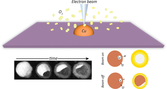
Environmental (scanning) transmission electron microscopy (E(S)TEM) has enabled sub-nanometer resolution imaging in gaseous environments and has thus provided a very useful tool to study gas–solid reactions.1−5 ETEM, in particular, has been applied in catalysis and provided fundamental insights into chemical reactions.6−8 Nonetheless, this technique requires high energy electrons to interact with the sample, and this may alter the sample and its properties. The electron beam-induced phenomena depend largely on the material under study but typically include sample heating, defect formation, phase transformation, charging, and ionization of the surrounding gases. Electron beam-induced changes in the local temperature are not trivial to quantify, and different approaches have been attempted to measure heat generation due to electron beam irradiation.9−12 Sample charging, due to the ejection of secondary, core, and Augur electrons, is another effect, which cannot be neglected in in situ E(S)TEM studies of electrodes, electrocatalysts, and catalytic redox reactions.13,14 In these cases, the electron beam-induced potential can be in the order of the redox potential of the desired reaction15 and thus needs to be carefully addressed. Electron beam-induced atomic displacement, known as the knock-on damage, causes the formation of interstitials and vacancies inside the sample16 and can lead to structural changes such as nanoparticle reorientation,17 re-crystallization,18−20 enhancement of diffusional process,21,22 and mechanical deformations.23 For instance, electron beam-induced local regions of dislocations in the Al-4Cu interface have been shown to enhance plastic deformation.24 In the case of metallic nanoparticle oxidation, it is reported that electron beam irradiation accelerates oxidation and inner void formation (nano Kirkendall (NK) effect).22,25 The NK effect in metallic nanoparticles is caused by the higher diffusion rate of metal ions through the oxide shell than inward diffusion of oxygen ions.26 It has been speculated that the electron beam will enhance this effect through the creation of vacancies, which will consequently increase the diffusion of interstitials and atoms.22 Another issue specific to ESTEM/ETEM studies is the interaction of the electron beam with the gas, leading to the ionization of the gas molecules through interaction with the high-energy incident electrons or even the back-scattered electrons emitted from the sample.1,27
Interestingly, the electron beam is not always a source of damage, and it has also been utilized as a tool for the fabrication of nanomaterials or triggering a chemical reaction. For example, electrons with an energy of 80–200 keV have been applied to etch multiwalled carbon nanotubes in oxygen.28 Another example is the use of focused electrons to reduce oxide nanotubes in specific regions, leading to the extraction and encapsulation of metal nanoparticles inside the nanotubes.29 Additionally, electron beam-induced fragmentation and deposition have been widely used to prepare metallic nanoparticles, believed to be instigated by beam-induced heating and charging.30−32 It can be concluded that the more we understand about the influence of high energy electrons on the sample in TEM, the more control we can exert over it, either as a beneficial tool in nano-manipulation and engineering or in minimizing its undesirable effects. Characterizing the influence of the electron beam in in situ studies such as E(S)TEM is particularly critical to separate its role from that of the applied stimuli in the investigation. Many such in situ studies involve the oxidation or reduction of metallic nanoparticles. In this regard, the oxidation of Cu nanoparticles is of interest due to its wide application in catalysis,33,34 electronic devices,35 photonics,36 and nanomedicine,37 and consequently, several accounts of in situ oxidation of Cu nanoparticles in E(S)TEM have been reported.5,38,39
Many reports suggest that electron beam irradiation affects the oxidation of solid materials. In some cases, the high energy electrons have been shown to enhance oxidation of metallic nanoparticles,22,40,41 while in others, it is believed to reduce or prevent it, e.g., as a result of cross-linking and formation of a carbon layer.42 Wang et al. suggested that beam-induced oxide layer growth in Fe nanoparticles is not due to particle heating or charging, but it is because of defect-mediated atomic displacements. Here, we have studied the oxidation of Cu nanoparticles in ESTEM at temperatures 100–200 °C. Using annular dark-field STEM (ADF STEM), we have recorded the morphological evolution of the particles during oxidation in real time and compared the oxidation rate of the particles with and without exposure to the electron beam. The results reveal that overall, electron beam exposure in ESTEM accelerates the oxidation of Cu nanoparticles. However, we observe that the electron beam counteractively enhances oxidation as a result of the outward diffusion of metallic ions and suppresses oxidation due to the inward diffusion of oxygen ions. The results demonstrate the important role that knock-on damage, charging, and ionization play in E(S)TEM investigations.
Results and Discussion
Polycrystalline Cu nanodiscs with an average diameter of ∼85 nm were fabricated by hole-mask colloidal lithography on DENSsolutions TEM heating chips. Prior to the experiments, the samples were annealed in 3 mbar of H2 at 400 °C for 1 h in the ETEM, resulting in their transformation into hemispherical Cu particles with fewer grains and an average diameter of 70 ± 7 nm (based on measurements from 20 particles). The samples were then oxidized in 3 mbar of O2 at temperatures 100, 125, 150, 175, and 200 °C. In each case, several particles were imaged continuously in situ by annular dark-field scanning TEM (ADF STEM) as oxidation progressed, with Figure 1 showing the ADF STEM images of the particles at the start and end time of the oxidation at each temperature. The magnification of the images, number of pixels per frame, probe dwell time per pixel, probe size and total current in the probe, and other microscope parameters (see Table 1) were kept unchanged between the experiments at different temperatures. At the end of each experiment, the O2 flow to the ETEM was stopped, the remaining O2 in the column was purged out and the samples were cooled down to room temperature. Once under high vacuum, the sample was moved to locate other particles on the same chip that had experienced the same oxidation conditions but had not been exposed to the electron beam during the reaction. In each case, ADF STEM images of 5–10 of these particles were recorded.
Figure 1.

Initial and final ADF STEM images of Cu particles oxidized in 3 mbar of O2 and at different temperatures while imaged in ESTEM.
Table 1. Experimental Parameters.
| temperature (°C) | 100 | 125 | 150 | 175 | 200 |
| frame size (pixel) | 1024 × 1024 | 1024 × 1024 | 1024 × 1024 | 1024 × 1024 | 1024 × 1024 |
| pixel dwell time (μs) | 2 | 2 | 2 | 2 | 2 |
| frame time (s) | 2.6 | 2.6 | 2.6 | 2.6 | 2.6 |
| pixel size (pm) | 608 | 608 | 608 | 608 | 608 |
| dose (e–/nm–2) | 1000 | 1000 | 1000 | 1000 | 1000 |
| total number of frames | 1984 | 1063 | 308 | 157 | 66 |
As described elsewhere,43 oxidation of Cu particles under similar conditions involves chemical reactions at the phase boundaries, leading to the generation of Cu+ cations and O2– anions, and the transport of these ions through an existing oxide layer for further reaction between the reactants and additional oxide formation. As Cu+ cations and O2– anions are produced at two separate phase boundaries (inner and outer interfaces of the oxide layer, respectively) and diffuse through the oxide layer in opposite directions, two separate oxide shells can be identified, an outer oxide shell growing outward from the original surface of the Cu nanoparticle and an inner oxide shell growing inward (see Section S1 in the Supporting Information (SI)). Moreover, Kirkendall void formation during the oxidation of Cu nanoparticles due to the faster diffusion of Cu+ cations relative to O2– anions is widely observed.44−46 We have previously reported the following sequence for the oxidation of Cu nanoparticles: oxide island nucleation, their growth and formation of continuous oxide shells, and Kirkendall void nucleation and expansion until the particles are fully oxidized and transformed into hollow particles with double oxide shells5 (see SI Section S1). This process is captured in the ADF STEM images, and while the contrast there is strongly related to the atomic number/thickness of the imaged species, contrast due to diffraction effects is also present in the images and is non-negligible. Therefore, segmenting the images based simply on intensity thresholding could not be applied to quantify the amount of metallic Cu lost and the oxide formed as a function of time during each reaction. Instead, the images were segmented based on the trends describing the evolution of each voxel in the time-series (with x and y dimensions in space and z dimension in time) as well as the spatial location of each of the substrate, oxide, and void, relative to the metallic core of the particles (see SI Videos V_100C – V_200C). A detailed description of the applied procedure can be found in Section S2 of the SI. Figure 2 shows the selected images of a particle oxidized at 100 °C and their corresponding segmented images.
Figure 2.

(a) Selected frames (approx. every 100 frames) from the ADF STEM image series of a Cu particle undergoing oxidation at 100 °C and (b) the corresponding segmented images.
To compare the oxidation rate at different temperatures,
particles
with similar sizes were selected, as shown in Figure 3a, and their images were segmented to obtain
changes in the metal and oxide volumes during oxidation (see SI Sections S2 and S3 for more details). The plot
of the fractional volume of the metal core lost during oxidation,
δ, as a function of time is presented in Figure 3b. We have previously shown that the fractional
volume of Cu particles oxidized under similar conditions can be modeled
with a Johnson–Mehl–Avrami–Kolmogorov (JMAK)
kinetic model5 of the form δ = 1
– exp ( – (kt)n), and the results presented in Figure 3b confirm this. The temperature-dependent
rate constant, k, follows the Arrhenius equation, 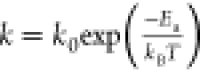 , where k0 is
the pre-exponential factor, Ea is the
activation energy, and kB is the Boltzmann
constant. Plotting our experimentally determined Ln(k) values versus the inverse of the nominal temperature shown in Figure 3c gives an apparent
activation energy of Ea = 0.5 eV (48.6
kJmol–1). While this is within the range of previously
reported values,44,47 it is based on measurements from
particles exposed to energetic electrons during oxidation, which is
likely to have influenced the reaction kinetics.
, where k0 is
the pre-exponential factor, Ea is the
activation energy, and kB is the Boltzmann
constant. Plotting our experimentally determined Ln(k) values versus the inverse of the nominal temperature shown in Figure 3c gives an apparent
activation energy of Ea = 0.5 eV (48.6
kJmol–1). While this is within the range of previously
reported values,44,47 it is based on measurements from
particles exposed to energetic electrons during oxidation, which is
likely to have influenced the reaction kinetics.
Figure 3.

(a) ADF STEM images of single Cu particles with similar sizes oxidized in 3 mbar of O2 and under electron beam irradiation at different temperatures prior to oxidation and at the end of the reaction. (b) Volume fraction of the metallic Cu core lost during oxidation, δ, as a function of time for each of the particles in (a) determined from the segmented image series of the particles. The experimentally determined values (*) are fitted with the JMAK model (solid lines), and the extracted rate constants, k, are used to obtain the activation energy of the reaction from the Arrhenius plot shown in (c).
To examine the influence of continual exposure to the electron beam during oxidation, Cu particles imaged during the reaction (beam-on) were compared with particles of similar sizes present on the same chip that had not been exposed to the electron beam (beam-off). Close-up images of beam-off particles recorded at the end of the reaction at the different temperatures are presented in Figure 4a. The volume fraction of the particles oxidized, δ, in each case is noted on the images, and as reference, images of beam-on particles at times when they had experienced the same oxidation fractions are shown in Figure 4b. Comparing the beam-on and beam-off particles in Figure 4a,b reveals that the electron beam had undoubtedly accelerated the reaction as the beam-on particles at all temperatures had reached equal δ values at an earlier time during the reaction relative to their corresponding beam-off particles. The extent of this acceleration, however, appears to have a temperature dependence, with larger differences observed between the times at which beam-off and beam-on particles reach equal oxidation fractions at lower temperatures (see Figure 4a,b), indicating the greater influence of the electrons on reaction rates at lower temperatures. Quantifying this electron beam-induced increase in reaction rate in terms of an apparent rise in temperature, ΔTapparent, we obtain values ranging from 30 to 6 °C for the nominal temperatures 100–200 °C, as plotted in Figure 4e (details can be found in SI Section S4). This confirms that the influence of the electron beam on the reaction is more pronounced at lower temperatures. Besides impacting the reaction rate, exposure to the electron beam appears to have also influenced the morphology of the particles. Figure 4c shows the close-up images of the oxide layers formed on beam-off and beam-on particles at equal oxidation fractions. Consistently, the outer oxide layers on the beam-on particles appear smoother at these earlier stages of oxidation compared to beam-off particles, where the oxide layer does not appear to have formed a continuous layer yet. We speculate that this could be related to an increased number of nucleation sites for the oxide on the surface of the particles irradiated with the electron beam during oxidation. Additionally, on closer inspection, the contrast in the images suggests the presence of a more pronounced inner oxide shell in beam-off particles. This is seen more clearly after the formation of the nano Kirkendall void (see Figure 4d). Measuring the ratio between the inner and outer oxide shell thicknesses at different temperatures demonstrates a clear trend for the formation of thinner inner oxide layers in beam-on particles, as presented in Figure 4f. The outer and inner oxide shells of the nanoparticles are the respective consequences of the transport of Cu+ cations and O2– anions through the oxide. Thus, our observation of decline in the inner oxide shell thickness of the particles indicates a decline in the inward diffusion rate of O2– anions through the oxide as a result of exposure to the electron beam.
Figure 4.

(a) ADF STEM images of particles not imaged during oxidation (beam-off) at the end of the reaction and (b) ADF STEM images of particles imaged during the reaction (beam-on) at the time when the same volume fraction, δ, of the metal has been oxidized as in (a). (c, d) Zoomed in images of the highlighted features in (a) and (b) showing the inner and outer oxide layers of the particles. The dotted lines show the boundary between the two oxide layers. (e) Apparent temperature difference between the beam-on and beam-off particles calculated according to the description provided in SI Section S4. (f) Ratio of the thickness of the inner and outer oxide shells (tin and tout, respectively) for the beam-on and beam-off particles at different temperatures.
To test the influence of the electron dose on these observations, we repeated the ESTEM oxidation of Cu particles at 200 °C using half the pixel dwell-time and thus half the electron dose previously applied. Changes in the volume fraction of the particle oxidized while imaged in ESTEM as a function of time alongside that for the particle oxidized under the same conditions but higher electron dose rates (cf. Figure 3) are shown in Figure 5. The results clearly indicate that the observed reaction kinetics have an electron dose dependence.
Figure 5.

Oxidation of Cu nanoparticles while exposed to a lower electron beam dose, with (a) showing the initial (0 s time) and final (243 s time) images of the particles in the recorded series. (b) Selected images of one of the particles at different times during oxidation. (c) Comparison between the time evolution of the metal volume fraction lost, δ, during oxidation under electron beam dose D1 = 1000 e–/nm2 applied in the results presented in Figures 2–4 and D2 = 500 e–/nm2 applied in (a) and (b) here.
Based on our observations, we can conclude that the electron beam clearly influences the oxidation of Cu nanoparticles. While it overall accelerates the reaction, this appears to be primarily related to the increase in the growth rate of the outer oxide shell of the particles. Conversely, we observe that electron beam exposure decelerates the growth rate of the inner oxide shell. Moreover, we find that the beam plays a more significant role at lower temperatures as well as at higher electron doses. As described by Hauffe,43 the key steps in solid-state oxidation of metals are as follows: (i) reactions at the phase boundaries, converting the metal into cations plus electrons (at the oxide–metal interface) and converting O2 molecules into anions after chemisorption and electron exchange (at the oxide–gas interface); (ii) diffusion of the produced ions and electrons through the existing oxide layer, necessary for subsequent reaction between the reactants and further oxide formation; and (iii) space-charge effects in case of very thin oxide layers and at lower temperatures. It is therefore appropriate to consider possible mechanisms through which electron beam exposure can influence these steps.
First, we examine sample heating by the electrons as the possible mechanism behind the observed enhanced oxidation of the particles. There are several approaches to calculate electron beam-induced heating.12,16,48,49 Here, we consider the model developed by Liu and Risbud,49 which is intended for nanoparticles and assumes thermal loss only through the particles (ignoring the substrate). In this case, the temperature increase is calculated using the following equation:
| 1 |
where J is the current density, e is the electron charge, R is the particle radius, cv is the specific heat of the material, ρ is the mass density, α is the thermal diffusivity, and Q is the total energy loss of the electron going through the material. Using eq 1, we calculate 2 °C heating of the sample when fully metallic and 9 °C when fully oxidized under the experimental conditions applied in Figures 1–4 (see SI Section S5 for details). As eq 1 does not consider heat dissipation through the substrate, it is likely to overestimate beam-induced heating. Applying the alternative model developed by Egerton et al.,16 which includes both thermal absorption and dissipation, we calculate negligible temperature increases below 10–2 °C by the electron beam under the same conditions (see SI Section S5 for details). Regardless of the model applied, the theoretical heating of the sample by the electron beam under the ESTEM conditions applied here is generally lower than the beam-induced effects observed, and thus, heating cannot be the main mechanism behind them. Furthermore, an electron beam-induced temperature increase cannot explain the impedance of O2– diffusion and the formation of thinner inner oxide layers nor the non-uniform influence of the electrons on the reaction rate at different temperatures (cf. Figure 4). It is, therefore, apt to conclude that an alternative mechanism must be behind the phenomena observed here.
As described by Sundarajan et al.,22 the primary electrons in TEM are typically sufficiently energetic to locally dislodge and eject atoms from their crystal sites through transfer of kinetic energy (often referred to as knock-on damage). Considering elastic scattering of the primary electrons deflected by the electrostatic field of stationary nuclei in the sample, the maximum energy transfer from the incident beam to the target atom is calculated by16
| 2 |
where E0 is the incident beam energy, m0 is the rest mass of an electron, and M is the nucleus mass. If this transferred energy from the incident beam exceeds an atomic displacement energy, the atom can get ejected from its site. Using eq 2, we obtain Emax = 13.4 eV for Cu irradiated with 300 keV electrons. This value is below the bulk displacement energy of Cu atoms (19 eV for (100) crystal plane). Albeit, since the atomic nuclei in the sample are not in fact stationary, the provision of this additional kinetic energy from the primary electron beam can enable already vibrating atoms to escape and become mobile50 (see SI Section 6). More crucial to the reaction, however, is the displacement and ionization of Cu at the oxide phase boundary and its diffusion through the oxide layer, as described above in steps (i) and (ii). Given the rough morphology and the polycrystalline nature of the oxide layer, we expect the displacement energy of Cu at the interface to be lower than the bulk value and Emax in this case to be above the threshold to displace and mobilize Cu at the metal–oxide interface. Interestingly, previous studies have identified the extraction of Cu from the lattice to be the rate limiting step in its oxidation,51 supporting the significant role that electron beam knock-on damage to Cu can have on enhancing its oxidation rate. In contrast, we do not expect kinetic energy transfer from the electron beam to have the same favorable impact on the generation rate and transport of O2– anions as the source is in gas form. Diffusivity in the solid state is defined as the number of atomic jumps per second and is calculated according to22
| 3 |
where λ is the jump distance, z is the number of nearest neighbors, Cv is the probability that a given neighbor is vacant, υD is the Debye frequency, ΔGm is the free energy maximum (per mole) along the diffusion path, R̅ is the universal gas constant, and T is the temperature. Kinetic energy transfer from the electron beam and knock-on damage affect parameters such as Cv and ΔGm in eq 3, resulting in enhanced diffusivity. As diffusivity is a thermally activated process, increasing the temperature will also increase the diffusion rate. Accordingly, beyond a certain temperature, thermal diffusion of ions surpasses and dominates over the effect of kinetic energy transfer from the electron beam. This leads to smaller differences between the oxidation extent of beam-on and beam-off particles at higher temperatures, as observed here (cf. Figure 4a,e).
While kinetic energy transfer from the electron beam accounts for the increased oxidation rate of the particles and its more pronounced influence at lower temperatures, it does not fully explain the suppressed growth rate of the inner oxide shell of the particles. We now consider electron beam-induced charging and ionization of the sample. A consequence of the interaction between the electron beam and the sample is the inelastic electron–electron collisions, giving rise to a fraction of electrons that are kicked out of atomic shells or bands, in the form of secondary or Auger electrons. This has been shown to lead to positive charge accumulation on solid specimens in TEM and the build-up of an electric potential of up to a few volts.15,52,53 Similarly, the interaction of the electron beam with the gas in ETEM gives rise to the ionization of gas molecules, and N2+ ions have been shown to be the most common product in a N2 environment.27 Secondary electron (SE) emission is the main source of electron beam-induced charging. Since SEs can only escape from the top surface of specimens, this leads to positive charge accumulation on the surface of our hemispherical nanoparticles and the formation of an outward radial electric field from their surface (see SI Section S7). In the case of the O2 gas, SE emission produces positively charged ions, with O2+ likely to be the most common product. The generated O2+ ions are, however, repelled by the positively charged surface of the nanoparticles, with the overall consequence of a lower diffusion rate of O2– anions through the oxide and a slower growth of the inner oxide shell. Based on our results, SE emission and charge accumulation on the surface of the particles do not have the same adverse effect on the diffusion rate of Cu+ cations, implying that the effect of kinetic energy transfer to Cu+ cations supersedes that of the induced electric field. The extents to which both kinetic energy transfer and charging effects influence the reaction rate naturally depend on the irradiation dose in ESTEM, with our results indicating lower dose imaging at higher temperatures to provide preferred conditions for minimizing the electron beam effects in ESTEM oxidation of Cu.
Conclusions
In conclusion, we have studied the effect of electron beam irradiation in ESTEM oxidation of Cu nanoparticles at temperatures 100–200 °C. We find that the electron beam actively influences the reaction and overall accelerates the oxidation of Cu nanoparticles. This acceleration is primarily due to the enhanced diffusion of Cu+ cations, which migrate outward and form an oxide shell on the outer surface of the particles at an increased rate. In contrast, the electron beam suppresses the inward diffusion of O2– anions, leading to the slower growth rate of an oxide shell below the surface of the nanoparticles. Moreover, we find that these electron beam-induced effects are significant to a larger extent at lower temperatures, and their influence wanes with increasing temperature as well as with reducing the electron dose. Our results suggest that the role of the electron beam in ESTEM oxidation of nanoparticles is mostly related to (1) kinetic energy transfer from the energetic electrons to the particles, giving rise to knock-on damage and increased generation rate and mobility of Cu+ and (2) ionization due to inelastic events such as secondary electron emission, leading to positive charge build-up on the surface of the particles and ionization of the O2 molecules into O2+ and thus inhibiting the diffusion of oxygen into the particles. Under moderate electron beam dose rates, the influence of the electron beam on the reaction at 200 °C was largely reduced, implying that at higher temperatures, close to unperturbed insights into reactions at the sub-nanometer scale can be obtained in ESTEM with careful electron beam dose management.
Methods
Nanoparticle Fabrication
The Cu nanoparticles were nanofabricated on Wildfire chips from DENSsolutions by hole-mask colloidal lithography.54 The following procedure was applied for the fabrication:
-
1.
Spin coating a thin layer of poly(methyl methacrylate), PMMA A4, resist in Anisole (MicroChem Corporation) at 1500 rpm for 60 s followed by 5 min heat treatment on a hotplate at 170 °C.
-
2.
5 s O2 plasma treatment (50 W, 10 sccm) to make the PMMA surface hydrophilic.
-
3.
Applying a drop of poly(diallyldimethylammonium chloride) polyelectrolyte (Sigma Aldrich) diluted in water to 0.2 wt % to the surface followed by 40 s of incubation.
-
4.
Drop coating the surface of the TEM chip with aqueous sulfonthiate latex polystyrene bead suspension with approximate particle sizes of 100 nm and a subsequent 3 min incubation.
-
5.
Deposition of 15 nm of Cr at the rate of 1 Å/s (Lesker PVD 225) followed by gentle wiping of the substrates with a wet tissue to remove the polystyrene beads and exposing the holes in the Cr mask without breaking the TEM membrane.
-
6.
5 min application of O2 plasma (50 W, 10 sccm) to etch the PMMA layer through the holes in the Cr mask down to the substrate.
-
7.
Deposition of 20 nm of Cu at the rate of 1 Å/s followed by mask lift-off in acetone for approximately 24 h.
ESTEM Imaging
In situ STEM imaging was performed using
an 80–300 kV FEI Titan Environmental TEM equipped with a field
emission gun. The ETEM instrument was operated at 300 kV in annular
dark-field STEM mode with an electron probe convergence semi-angle
of 10 mrad, detector inner-collection angle of 35 mrad, and probe
size of approximately 0.2 nm. A probe current of 30 pA, calibrated
using a Faraday cup setup, was used in the experiments, and the STEM
electron dose was calculated according to the equation  , where I is the beam current, tp is the pixel dwell time of the images, and Ap is the pixel area. The Cu nanoparticles were
fabricated directly on DENSsolutions Wildfire chips to enable controlled
heating of the samples inside the TEM. First, the Cu nanoparticles
were thermally annealed inside the ETEM but without exposure to the
electron beam at 400 °C and in 3 mbar of H2 atmosphere
for 1 h. This was to remove hydrocarbons and to recrystallize the
particles. Following annealing, STEM images of the particles were
recorded continuously while exposed to 3 mbar O2 until
the particles were mostly oxidized. At the end, the flow of O2 was stopped, the microscope was set to high vacuum conditions,
and STEM images of nanoparticles that had not been exposed to the
electron beam were recorded. The experiment was conducted at temperatures
100, 125, 150, 175, and 200 °C.
, where I is the beam current, tp is the pixel dwell time of the images, and Ap is the pixel area. The Cu nanoparticles were
fabricated directly on DENSsolutions Wildfire chips to enable controlled
heating of the samples inside the TEM. First, the Cu nanoparticles
were thermally annealed inside the ETEM but without exposure to the
electron beam at 400 °C and in 3 mbar of H2 atmosphere
for 1 h. This was to remove hydrocarbons and to recrystallize the
particles. Following annealing, STEM images of the particles were
recorded continuously while exposed to 3 mbar O2 until
the particles were mostly oxidized. At the end, the flow of O2 was stopped, the microscope was set to high vacuum conditions,
and STEM images of nanoparticles that had not been exposed to the
electron beam were recorded. The experiment was conducted at temperatures
100, 125, 150, 175, and 200 °C.
Image Analysis
The frame-to-frame spatial drift in the recorded STEM image series was corrected initially by maximizing the cross-correlation coefficient between successive frames. This was carried out on the full frames containing multiple particles using the DigitalMicrograph software. The remaining spatial drift in the images was corrected on cropped frames containing individual particles using the center of mass method. First, binary thresholding was applied followed by erosion operation. After that, the center of mass of the group of pixels belonging to the whole particle was determined using connected component analysis. The center of mass served as the point around which each image was cropped. For the analysis, particles with similar sizes at different temperatures were selected. In each case, the images were segmented into four different categories (namely, substrate, metal, oxide, and void) using the purpose written Matlab script “SpaceTimeAnalysis.m” that compares the profile of each voxel in the image stacks to those from sampled regions in the images, as described in SI Section S2. Subsequently, the total number of pixels belonging to each segmented category in the images was counted and converted to area. In the case of the remaining metal in each frame, the calculated area was converted to volume using the method described in SI Section S3, assuming that the particles have close to hemispherical shapes, and the fraction of the metal volume lost (due to oxide formation) relative to the initial phase of the particle was calculated for each frame accordingly.
Acknowledgments
A.Z. and S.K. acknowledge financial support from VILLUM FONDEN (research grant 36155). S.N. and C.L. acknowledge financial support from the Knut and Alice Wallenberg Foundation project 2015.0055 and the Swedish Research Council (VR) Consolidator Grant project 2018-00329. Part of this work was carried out at the MC2 cleanroom facility.
Supporting Information Available
The Supporting Information is available free of charge at https://pubs.acs.org/doi/10.1021/acsnanoscienceau.3c00018.
Composition analysis of particles; details of image segmentation; details of metal volume calculation; details of converting the beam effect to temperature increase; electron beam-induced heating; electron beam-induced knock-on damage; electron beam-induced charging (PDF)
Recorded ADF STEM image series of the particles during oxidation alongside the segmented images for each frame at 100, 125, 150, 175, and 200 °C (ZIP)
Author Contributions
CRediT: Azin Ziashahabi data curation (supporting), formal analysis (supporting), investigation (equal), methodology (supporting), writing-original draft (equal); Anna Elsukova formal analysis (supporting), methodology (supporting), software (supporting), visualization (equal), writing-review & editing (supporting); Sara Nilsson data curation (equal), investigation (equal), writing-review & editing (equal); Marco Beleggia formal analysis (equal), methodology (supporting), validation (supporting), writing-review & editing (equal); Peter Stanley Jørgensen formal analysis (supporting), visualization (equal), writing-review & editing (equal); Christoph Langhammer funding acquisition (supporting), resources (equal), supervision (supporting), validation (equal), writing-review & editing (equal); Shima Kadkhodazadeh conceptualization (lead), data curation (lead), formal analysis (equal), funding acquisition (lead), investigation (equal), methodology (equal), project administration (lead), supervision (lead), validation (equal), visualization (equal), writing-original draft (equal), writing-review & editing (equal).
The authors declare no competing financial interest.
Supplementary Material
References
- Hansen T. W.; Wagner J. B.; Dunin-Borkowski R. E. Aberration Corrected and Monochromated Environmental Transmission Electron Microscopy: Challenges and Prospects for Materials Science. Mater. Sci. Technol. 2010, 26, 1338–1344. 10.1179/026708310X12756557336355. [DOI] [Google Scholar]
- Jinschek J. R. Advances in the Environmental Transmission Electron Microscope (ETEM) for Nanoscale in Situ Studies of Gas-Solid Interactions. Chem. Commun. 2014, 50, 2696–2706. 10.1039/C3CC49092K. [DOI] [PubMed] [Google Scholar]
- Boyes E. D.; Gai P. L. Environmental High Resolution Electron Microscopy and Applications to Chemical Science. Ultramicroscopy 1997, 67, 219–232. 10.1016/S0304-3991(96)00099-X. [DOI] [Google Scholar]
- Sjökvist R.; Tornberg M.; Marnauza M.; Jacobsson D.; Dick K. A. Observation of the Multilayer Growth Mode in Ternary InGaAs Nanowires. ACS Nanosci. Au 2022, 2, 539–548. 10.1021/acsnanoscienceau.2c00028. [DOI] [PMC free article] [PubMed] [Google Scholar]
- Nilsson S.; Nielsen M. R.; Fritzsche J.; Langhammer C.; Kadkhodazadeh S. Competing Oxidation Mechanisms in Cu Nanoparticles and Their Plasmonic Signatures. Nanoscale 2022, 14, 8332–8341. 10.1039/D2NR01054B. [DOI] [PubMed] [Google Scholar]
- Yoshida H.; Kuwauchi Y.; Jinschek J. R.; Sun K.; Tanaka S.; Kohyama M.; Shimada S.; Haruta M.; Takeda S. Visualizing Gas Molecules Interacting with Supported Nanoparticulate Catalysts at Reaction Conditions. Science 2012, 335, 317–319. 10.1126/science.1213194. [DOI] [PubMed] [Google Scholar]
- Gai P. L. Direct Probing of Gas Molecule-Solid Catalyst Interactions on the Atomic Scale. Adv. Mater. 1998, 10, 1259–1263. . [DOI] [Google Scholar]
- Kadkhodazadeh S.; Cavalca F. C.; Miller B. J.; Zhang L.; Wagner J. B.; Crozier P. A.; Hansen T. W. In Situ TEM under Optical Excitation for Catalysis Research. Top. Curr. Chem. 2022, 380, 52. 10.1007/s41061-022-00408-3. [DOI] [PubMed] [Google Scholar]
- Guo H.; Zhou P.; Natelson D.; Lou J. Quantification of Electron Beam Heating Effect in TEM. Microsc. Microanal. 2017, 23, 1766–1767. 10.1017/S1431927617009497. [DOI] [Google Scholar]
- Wang Z.; Gui L.; Han D.; Xu Z.; Han L.; Xu S. Measurement and Evaluation of Local Surface Temperature Induced by Irradiation of Nanoscaled or Microscaled Electron Beams. Nanoscale Res. Lett. 2019, 14, 31. 10.1186/s11671-018-2821-x. [DOI] [PMC free article] [PubMed] [Google Scholar]
- Park J.; Bae K.; Kim T. R.; Perez C.; Sood A.; Asheghi M.; Goodson K. E.; Park W. Direct Quantification of Heat Generation Due to Inelastic Scattering of Electrons Using a Nanocalorimeter. Adv. Sci. 2021, 8, 2002876. 10.1002/advs.202002876. [DOI] [PMC free article] [PubMed] [Google Scholar]
- Kryshtal A.; Mielczarek M.; Pawlak J. Effect of Electron Beam Irradiation on the Temperature of Single AuGe Nanoparticles in a TEM. Ultramicroscopy 2022, 233, 113459 10.1016/j.ultramic.2021.113459. [DOI] [PubMed] [Google Scholar]
- Jooss C.; Mildner S.; Beleggia M.; Mierwaldt D.; Roddatis V.. ETEM Studies of Electrodes and Electro-Catalysts. Controlled Atmosphere Transmission Electron Microscopy: Principles and Practice; Springer, 2016, 301–329. [Google Scholar]
- Raabe S.; Mierwaldt D.; Ciston J.; Uijttewaal M.; Stein H.; Hoffmann J.; Zhu Y.; Blöchl P.; Jooss C. In Situ Electrochemical Electron Microscopy Study of Oxygen Evolution Activity of Doped Manganite Perovskites. Adv. Funct. Mater. 2012, 22, 3378–3388. 10.1002/adfm.201103173. [DOI] [Google Scholar]
- Mildner S.; Beleggia M.; Mierwaldt D.; Hansen T. W.; Wagner J. B.; Yazdi S.; Kasama T.; Ciston J.; Zhu Y.; Jooss C. Environmental TEM Study of Electron Beam Induced Electrochemistry of Pr0.64Ca0.36MnO3 Catalysts for Oxygen Evolution. J. Phys. Chem. C 2015, 119, 5301–5310. 10.1021/jp511628c. [DOI] [Google Scholar]
- Egerton R. F.; Li P.; Malac M. Radiation Damage in the TEM and SEM. Micron 2004, 35, 399–409. 10.1016/j.micron.2004.02.003. [DOI] [PubMed] [Google Scholar]
- Azcárate J. C.; Fonticelli M. H.; Zelaya E. Radiation Damage Mechanisms of Monolayer-Protected Nanoparticles via TEM Analysis. J. Phys. Chem. C 2017, 121, 26108–26116. 10.1021/acs.jpcc.7b08525. [DOI] [Google Scholar]
- Bae I. T.; Zhang Y.; Weber W. J.; Higuchi M.; Giannuzzi L. A. Electron-Beam Induced Recrystallization in Amorphous Apatite. Appl. Phys. Lett. 2007, 90, 21912. 10.1063/1.2430779. [DOI] [Google Scholar]
- Danielsen H. K.; Kadkhodazadeh S.; Grumsen F. B.; Somers M. A. J. New Amorphous Interface for Precipitate Nitrides in Steel. Philos. Mag. 2014, 94, 2339–2349. 10.1080/14786435.2014.913112. [DOI] [Google Scholar]
- Jenc̆ic̆ I.; Bench M. W.; Robertson I. M.; Kirk M. A. Electron Beam Induced Crystallization Of Isolated Amorphous Regions In Si, Ge, GaP, And GaAs. J. Appl. Phys. 1995, 78, 974–982. 10.1063/1.360764. [DOI] [Google Scholar]
- Egerton R. F.; McLeod R.; Wang F.; Malac M. Basic Questions Related to Electron-Induced Sputtering in the TEM. Ultramicroscopy 2010, 110, 991–997. 10.1016/j.ultramic.2009.11.003. [DOI] [Google Scholar]
- Sundararajan J. A.; Kaur M.; Qiang Y. Mechanism of Electron Beam Induced Oxide Layer Thickening on Iron-Iron Oxide Core-Shell Nanoparticles. J. Phys. Chem. C 2015, 119, 8357–8363. 10.1021/acs.jpcc.5b00943. [DOI] [Google Scholar]
- Stangebye S.; Zhang Y.; Gupta S.; Zhu T.; Pierron O.; Kacher J. Understanding and Quantifying Electron Beam Effects during in Situ TEM Nanomechanical Tensile Testing on Metal Thin Films. Acta Mater. 2022, 222, 117441 10.1016/j.actamat.2021.117441. [DOI] [Google Scholar]
- Li S. H.; Han W. Z.; Shan Z. W. Deformation of Small-Volume Al-4Cu Alloy under Electron Beam Irradiation. Acta Mater. 2017, 141, 183–192. 10.1016/j.actamat.2017.09.015. [DOI] [Google Scholar]
- Wang C. M.; Baer D. R.; Amonette J. E.; Engelhard M. H.; Antony J. J.; Qiang Y. Electron Beam-Induced Thickening of the Protective Oxide Layer around Fe Nanoparticles. Ultramicroscopy 2007, 108, 43–51. 10.1016/j.ultramic.2007.03.002. [DOI] [PubMed] [Google Scholar]
- Yin Y.; Rioux R. M.; Erdonmez C. K.; Hughes S.; Somorjai G. A.; Alivisatos A. P. Formation of Hollow Nanocrystals Through the Nanoscale Kirkendall Effect. Science 2004, 304, 711–714. 10.1126/science.1096566. [DOI] [PubMed] [Google Scholar]
- Tokunaga T.; Kawakami T.; Higuchi K.; Yamamoto Y.; Yamamoto T. Effect of Electron Beam Irradiation in Gas Atmosphere during ETEM. Micron 2022, 158, 103289 10.1016/j.micron.2022.103289. [DOI] [PubMed] [Google Scholar]
- Yoshida H.; Tomita Y.; Soma K.; Takeda S. Electron Beam Induced Etching of Carbon Nanotubes Enhanced by Secondary Electrons in Oxygen. Nanotechnology 2017, 28, 195301. 10.1088/1361-6528/aa6a4c. [DOI] [PubMed] [Google Scholar]
- El Mel A.-A.; Molina-Luna L.; Buffière M.; Tessier P.-Y.; Du K.; Choi C.-H.; Kleebe H.-J.; Konstantinidis S.; Bittencourt C.; Snyders R. Electron Beam Nanosculpting of Kirkendall Oxide Nanochannels. ACS Nano 2014, 8, 1854–1861. 10.1021/nn406328f. [DOI] [PubMed] [Google Scholar]
- Caldwell M. A.; Haynor B.; Aloni S.; Ogletree D. F.; Wong H. S. P.; Urban J. J.; Milliron D. J. Spectroscopic Evidence for Exceptional Thermal Contribution to Electron Beam-Induced Fragmentation. J. Phys. Chem. C 2010, 114, 22064–22068. 10.1021/jp1078086. [DOI] [Google Scholar]
- Pyrz W. D.; Park S.; Vogt T.; Buttrey D. J. Electron Beam-Induced Fragmentation and Dispersion of Bi-Ni Nanoparticles. J. Phys. Chem. C 2007, 111, 10824–10828. 10.1021/jp071414i. [DOI] [Google Scholar]
- Herley P. J.; Jones W. The Generation of Nanoscale Metal Particles from Metal Azides - a High-Resolution Electron Microscopic Study. Z. Phys. D – At., Mol. Clusters 1993, 26, 159–161. 10.1007/BF01425650. [DOI] [Google Scholar]
- Gawande M. B.; Goswami A.; Felpin F. X.; Asefa T.; Huang X.; Silva R.; Zou X.; Zboril R.; Varma R. S. Cu and Cu-Based Nanoparticles: Synthesis and Applications in Catalysis. Chem. Rev. 2016, 116, 3722–3811. 10.1021/acs.chemrev.5b00482. [DOI] [PubMed] [Google Scholar]
- Xie H.; Wang J.; Ithisuphalap K.; Wu G.; Li Q. Recent Advances in Cu-Based Nanocomposite Photocatalysts for CO2 Conversion to Solar Fuels. J. Energy Chem. 2017, 26, 1039–1049. 10.1016/j.jechem.2017.10.025. [DOI] [Google Scholar]
- Majumdar D.; Ghosh S. Recent Advancements of Copper Oxide Based Nanomaterials for Supercapacitor Applications. J. Energy Storage 2021, 34, 101995 10.1016/j.est.2020.101995. [DOI] [Google Scholar]
- Böhme A.; Sterl F.; Kath E.; Ubl M.; Manninen V.; Giessen H. Electrochemistry on Inverse Copper Nanoantennas: Active Plasmonic Devices with Extraordinarily Large Resonance Shift. ACS Photonics 2019, 6, 1863–1868. 10.1021/acsphotonics.9b00716. [DOI] [Google Scholar]
- Zhong X.; Dai X.; Wang Y.; Wang H.; Qian H.; Wang X. Copper-Based Nanomaterials for Cancer Theranostics. Wiley Interdiscip. Rev.: Nanomed. Nanobiotechnol. 2022, 14, e1797 10.1002/wnan.1797. [DOI] [PubMed] [Google Scholar]
- LaGrow A. P.; Ward M. R.; Lloyd D. C.; Gai P. L.; Boyes E. D. Visualizing the Cu/Cu2O Interface Transition in Nanoparticles with Environmental Scanning Transmission Electron Microscopy. J. Am. Chem. Soc. 2017, 139, 179–185. 10.1021/jacs.6b08842. [DOI] [PubMed] [Google Scholar]
- Tokozakura D.; Nakamura R.; Nakajima H.; Lee J.-G.; Mori H. Transmission Electron Microscopy Observation of Oxide Layer Growth on Cu Nanoparticles and Formation Process of Hollow Oxide Particles. J. Mater. Res. 2007, 22, 2930–2935. 10.1557/JMR.2007.0362. [DOI] [Google Scholar]
- Latham A. H.; Williams M. E. Transmission Electron Microscope-Induced Structural Evolution in Amorphous Fe, Co, and Ni Oxide Nanoparticles. Langmuir 2008, 24, 14195–14202. 10.1021/la7035423. [DOI] [PubMed] [Google Scholar]
- Zhang H.; Xu T.; Zhu Y.; Wang W.; Zhang H.; Yuan D.; Sun L. In Situ Atomic-Scale Observation of Silver Oxidation Triggered by Electron Beam Irradiation. Nanomaterials 2021, 11, 1021. 10.3390/nano11041021. [DOI] [PMC free article] [PubMed] [Google Scholar]
- Koh A. L.; Bao K.; Khan I.; Smith W. E.; Kothleitner G.; Nordlander P.; Maier S. A.; Mccomb D. W. Electron Energy-Loss Spectroscopy (EELS) of Surface Plasmons in Single Silver Nanoparticles and Dimers: Influence of Beam Damage and Mapping of Dark Modes. ACS Nano 2009, 3, 3015–3022. 10.1021/nn900922z. [DOI] [PubMed] [Google Scholar]
- Hauffe K.The Mechanism of Oxidation of Metals—Theory; Springer US, 1995. [Google Scholar]
- Susman M. D.; Feldman Y.; Bendikov T. A.; Vaskevich A.; Rubinstein I. Real-Time Plasmon Spectroscopy Study of the Solid-State Oxidation and Kirkendall Void Formation in Copper Nanoparticles. Nanoscale 2017, 9, 12573–12589. 10.1039/C7NR04256F. [DOI] [PubMed] [Google Scholar]
- Rice K. P.; Paterson A. S.; Stoykovich M. P. Nanoscale Kirkendall Effect and Oxidation Kinetics in Copper Nanocrystals Characterized by Real-Time, In Situ Optical Spectroscopy. Part. Part. Syst. Charact. 2015, 32, 373–380. 10.1002/ppsc.201400155. [DOI] [Google Scholar]
- Nilsson S.; Albinsson D.; Antosiewicz T. J.; Fritzsche J.; Langhammer C. Resolving Single Cu Nanoparticle Oxidation and Kirkendall Void Formation with in Situ Plasmonic Nanospectroscopy and Electrodynamic Simulations. Nanoscale 2019, 11, 20725–20733. 10.1039/C9NR07681F. [DOI] [PubMed] [Google Scholar]
- Rice K. P.; Walker E. J.; Stoykovich M. P.; Saunders A. E. Solvent-Dependent Surface Plasmon Response and Oxidation of Copper Nanocrystals. J. Phys. Chem. C 2011, 115, 1793–1799. 10.1021/jp110483z. [DOI] [Google Scholar]
- Gryaznov V. G.; Kaprelov A. M.; Belov A. Y. Real Temperature of Nanoparticles in Electron Microscope Beams. Philos. Mag. Lett. 1991, 63, 275–279. 10.1080/09500839108214655. [DOI] [Google Scholar]
- Liu L.-C.; Risbud S. H. Real-time Hot-stage High-voltage Transmission Electron Microscopy Precipitation of CdS Nanocrystals in Glasses: Experiment and Theoretical Analysis. J. Appl. Phys. 1994, 76, 4576–4580. 10.1063/1.357291. [DOI] [Google Scholar]
- Susi T.; Meyer J. C.; Kotakoski J. Quantifying Transmission Electron Microscopy Irradiation Effects Using Two-Dimensional Materials. Nat. Rev. Phys. 2019, 1, 397–405. 10.1038/s42254-019-0058-y. [DOI] [Google Scholar]
- Nilsson S.; Posada-Borbón A.; Zapata-Herrera M.; Bastos Da Silva Fanta A.; Albinsson D.; Fritzsche J.; Silkin V. M.; Aizpurua J.; Grönbeck H.; Esteban R.; Langhammer C. Probing the Role of Grain Boundaries in Single Cu Nanoparticle Oxidation by in Situ Plasmonic Scattering. Phys. Rev. Mater. 2022, 6, 045201 10.1103/PhysRevMaterials.6.045201. [DOI] [Google Scholar]
- Peng X.; Tu Q.; Zhang Y.; Jun K.; Shen F.; Ogunfunmi T.; Sun Y.; Tucker M. C.; Ceder G.; Scott M. C. Unraveling Li Growth Kinetics in Solid Electrolytes Due to Electron Beam Charging. Sci. Adv. 2023, 9, eabq3285 10.1126/sciadv.abq3285. [DOI] [PMC free article] [PubMed] [Google Scholar]
- Zheng F.; Beleggia M.; Migunov V.; Pozzi G.; Dunin-Borkowski R. E. Electron-Beam-Induced Charging of an Al2O3 Nanotip Studied Using off-Axis Electron Holography. Ultramicroscopy 2022, 241, 113593 10.1016/j.ultramic.2022.113593. [DOI] [PubMed] [Google Scholar]
- Fredriksson H.; Alaverdyan Y.; Dmitriev A.; Langhammer C.; Sutherland D. S.; Zäch M.; Kasemo B. Hole–Mask Colloidal Lithography. Adv. Mater. 2007, 19, 4297–4302. 10.1002/adma.200700680. [DOI] [Google Scholar]
Associated Data
This section collects any data citations, data availability statements, or supplementary materials included in this article.