Abstract
In this paper, a frequency-locked loop (FLL) based multimodal readout integrated circuit (IC) for interfacing with off-chip temperature, electrochemical, and pH sensors is presented. By reconfiguring its switched-capacitor based feedback network, the readout circuit is able to measure resistance, current, and voltage without additional active analog front-end circuits and at very low power . A prototype IC was fabricated in a 0.18 μm CMOS process. Measured results show that when measuring resistance, the input-referred resistance resolution is 10.5Ω for 100 Hz integration bandwidth. Using an off-chip thermistor, the readout circuit covers a temperature range of 0–75°C and achieves an equivalent temperature resolution of 16.4mKrms at 9.2 μW operation. In current mode, the readout circuit has an input range of 0.5 μA and an input-referred current noise as low as 40.6 pArms for 100 Hz bandwidth at 6 μW operation. Interfacing with an on-chip potentiostat, glucose chronoamperometry is demonstrated. In voltage mode, a minimum input-referred voltage noise of 3.17 μVrms is achieved at 5.6 μW operation, and the IC can measure a pH range from 1.6 to 12 using a commercial pH probe. At a 1.2 V supply, power consumption of the readout circuit is below 10 μW for all three measurement modes. Additionally, the prototype IC includes an integrated wireless transmitter that implements on-off keying modulation, and a wireless multimodal sensing system utilizing the FLL-based readout circuit is demonstrated.
Index Terms—: FLL, temperature, pH, potentiostat, sensors
I. Introduction
Multimodal sensing of physiological information through minimally invasive means is critical for health monitoring, from clinical and consumer applications to sports medicine. For example, in the case of wound healing, an abnormal temperature fluctuation can be a sign of infection [1], [2], and pH levels can also indicate infection and healing progression of the wound [3]. In the case of diabetes management, blood glucose levels should be frequently monitored, as abnormal levels of glucose can damage organs. Finally, in exercise therapy, pH and lactate levels in sweat are related to exercise intensity and closely monitored in elite athletes [4], [5].
In these wearable point-of-care sensor systems, off-chip or on-chip transducers transform biophysical information to analog electrical signals. In general, transducers provide analog information in either resistance, voltage, or current domains. For example, temperature results in the change of conductance in a thermistor; ionic concentration affects the voltage of an electrochemical cell used to measure pH; and, metabolites such as glucose are quantitatively detected using current measurement via potentiostat circuits. In most wearable bio-monitors, these signals serve as the input to front-end interfacing readout circuits for signal amplification, conditioning, and digitization.
Given that analog signals from these transducers are often in different domains, conventional readout circuits consist of specialized analog front-end circuitry to convert an input signal to the voltage domain before performing sampling and quantization using a Nyquist-rate analog-to-digital converter (ADC), as shown in Fig. 1(a). A primary drawback of these architectures is that they require additional analog blocks to convert a signal to voltage domain, requiring additional power and area and generate excess noise.
Fig. 1:
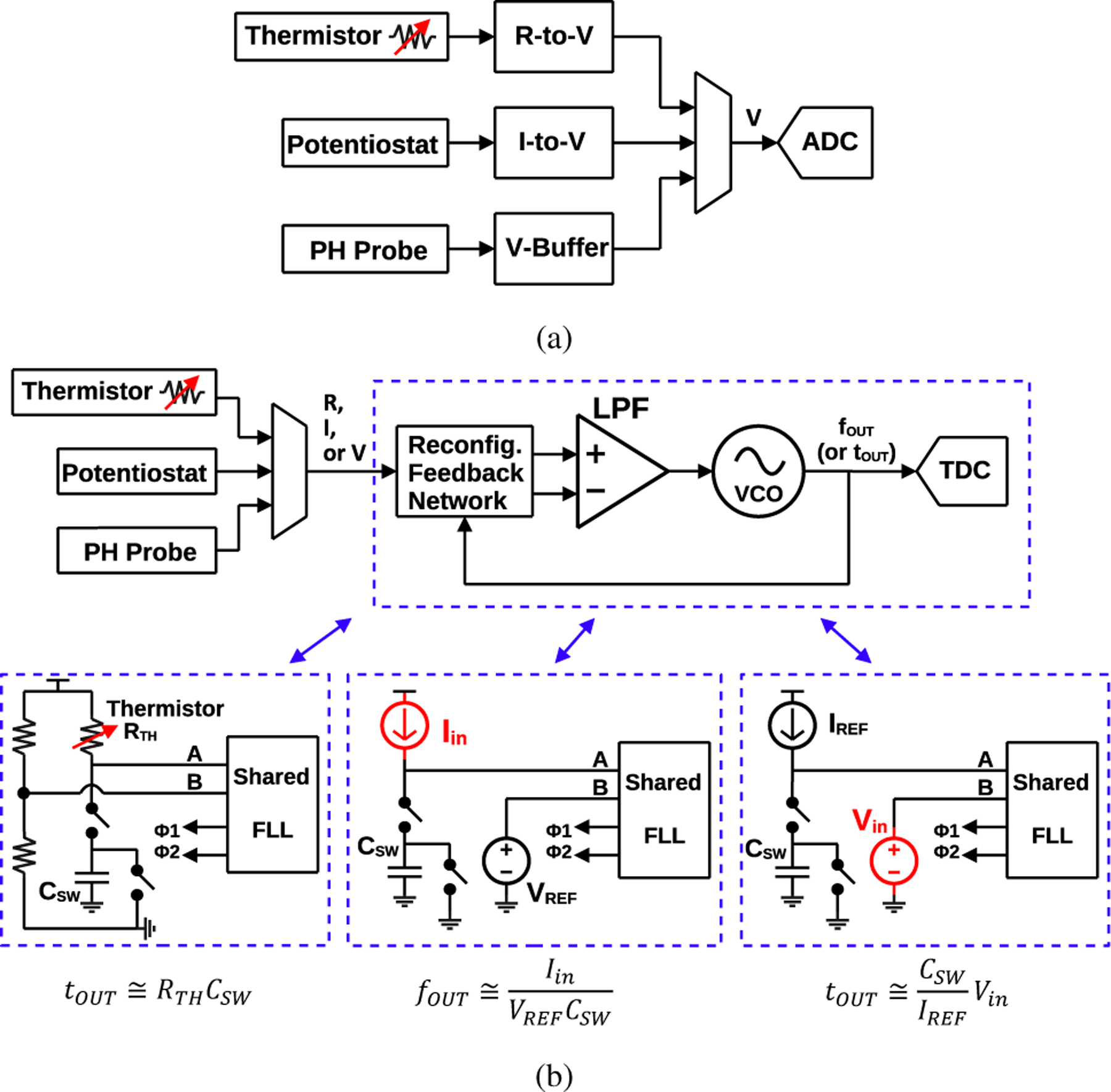
(a) Conventional multimodal sensor readout architecture, and (b) proposed reconfigurable FLL-based multimodal readout architecture.
As an alternative approach, we propose a frequency-locked loop (FLL) readout circuit that performs direct analog-to-digital conversion for resistance-, current-, and voltage-mode inputs by modifying the loop's feedback network. A conceptual block diagram is shown in Fig. 1(b). The first mode is resistance-to-period conversion, with the feedback network comprising a switched-capacitor (SC) Wheatstone Bridge (WhB). This enables the FLL to act as a temperature sensor in conjunction with an off-chip thermistor or resistive temperature detector (RTD). The second mode provides current-to-frequency conversion, where the input current of interest flows into the SC. In this way, the FLL, with the help of an on-chip potentiostat, can interface with glucose and lactate sensors using chronoamperometry (CA). In the third mode, voltage-to-period conversion is achieved by modifying the feedback network such that a reference current source flows into the SC; a high-impedance input is provided for voltage-mode transducers, such as an external pH probe. Embedding the voltage-controlled oscillator (VCO) in the FLL also enables time-domain quantization. An on-chip, oversampling time-to-digital converter (TDC) converts FLL frequency or period to a digital output. To display the versatility and low power consumption of the proposed readout circuit, it is implemented as a multimodal readout system-on-chip (SoC) that also includes a potentiostat and an on-off keying (OOK) transmitter. The complete wireless sensor system is demonstrated by interfacing with commercial, off-chip transducers.
This paper is an extension of our prior publication [6] and is organized as follows: Section II provides an overview of the functionality of the FLL, followed by detailed loop analysis in Section III; Section IV provides details of design and circuit implementation; Section V shows measurement setup and results; and conclusions are drawn in Section VI.
II. System Architecture
A. Background
The analog front-end (AFE) in a readout circuit used for multimodal biosensing should be capable of processing signals from different sensor sources. Common ADC architectures, such as power-efficient SAR ADCs, sample and quantize input in the voltage domain; as such, conventional AFE circuitry involves transforming analog signals to the voltage domain before performing additional analog or digital signal processing [7], [8]. However, for many electrochemical measurement techniques, such as chronoamperometry (CA) and cyclic voltammetry (CV), current is generated at the output of the chemical cell. In such cases, transimpedance amplifiers are often used to convert current to voltage [7], [9]-[11].
With the realization that current is the dominant signal of interest for many biochemical sensors, a recent trend in SoC design involves the integration of current-mode ADCs directly into the sensor system. For example, taking advantage of the low bandwidth nature of the current signal, low-order Delta-Sigma modulators have been used to digitize current directly [12]. At the same time, frequency-domain and time-domain quantization techniques have become increasingly popular. In [1], [9], [13], [14], relaxation oscillators translate potentiostat output current to frequency, and time-to-digital converters quantize the output frequency. However, the challenge of signal domain conversion still remains for multimodal sensing, where a current-mode ADC requires additional voltage-to-current conversion when performing a voltage-domain measurement, such as pH [14], [15].
Meanwhile, for resistive measurements, FLL-based readout architectures have shown advantages in linearity and resolution [16]-[18]. By inserting a VCO in an analog feedback loop, VCO nonlinearity is greatly suppressed by the loop gain, such that the readout circuit does not suffer from limited input range [19] or require downstream linearization [20]. Also, since VCOs are commonly implemented using multi-stage ring oscillators, TDCs that oversample the VCO phases enable first-order noise shaping and finer quantization resolution [21].
To satisfy the need of interfacing with resistance-, current-, and voltage-domain sensors, we designed a tri-mode readout circuit whose conceptual block diagram is shown in Fig. 1 (b).
B. Resistance-to-Period Mode
For measuring resistive sensors, a Wheatstone Bridge (WhB) is used in an FLL-based readout circuit to function as a resistance-to-period converter [17], [18]. As shown in Fig. 2(a), the frequency (or period) of the dual-phase clock sets the equivalent resistance of a switched capacitor, , inside the feedback network. A properly designed ratio (M) between and ensures incomplete settling on node A [17], and the equivalent resistance of the SC is
| (1) |
where and are the oscillation frequency and period of the VCO, respectively. In steady-state, the frequency of the VCO is "locked" such that nodes A and B are balanced by the feedback mechanism. A decrease in thermistor resistance causes a decrease in VCO period, such that the WhB stays balanced, and vice versa. The resistance-mode readout circuit in this work is explicitly designed for an off-chip thermistor or RTD, as would be integrated into a wearable device. To enable variable power consumption, two voltage regulators provide adjustable voltages for top and bottom voltage supply rails of the WhB [22].
Fig. 2:
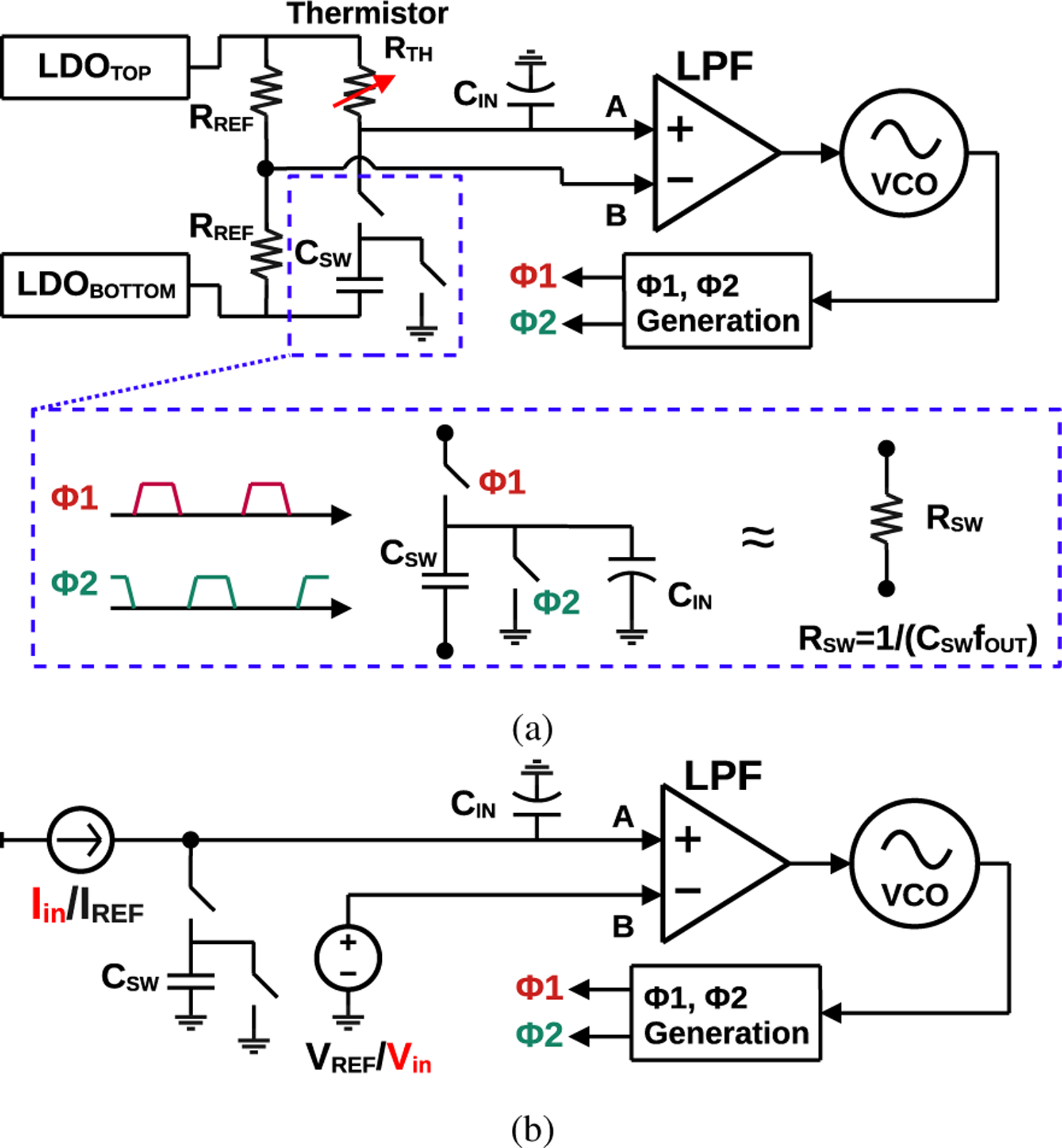
(a) Block diagram of resistance-mode operation, and (b) block diagram of current- or voltage-mode operation.
C. Current-to-Frequency and Voltage-to-Period Modes
The FLL architecture can also be used as a multimodal readout circuit for current and voltage, in addition to resistance and capacitance sensing. Intuitively, the WhB right leg can be considered as a current injecting into the SC equivalent resistance, while the left leg provides a voltage reference. As such, the differential input to the error amplifier is effectively controlled by the magnitude of current injection. Fig. 2(b) illustrates how the FLL can be controlled by a current or voltage input signal. We can further define the large-signal relationship between input current and VCO frequency as
| (2) |
where is the voltage given to the negative input of the low pass filter (LPF), is the DC gain of the LPF, and is the VCO voltage-to-frequency gain. At first glance, one would note that the relation between and is not linear, as also appears in the denominator on the right side of the equation. However, if we write the equation as
| (3) |
and assume that LPF and VCO gain are large at DC, then the current-to-frequency relationship can be approximated as
| (4) |
As shown, the nonlinear frequency term in equation (3) is attenuated by the large DC gain of the LPF and VCO. To demonstrate the resulting linearity of current-to-frequency conversion, Fig. 3(a) shows the magnitude of nonlinearity error versus LPF DC gain, assuming and are chosen such that 0–1 μA of current is translated to 0–1 MHz of frequency change. As can be seen in Fig. 3(b), even for a moderate LPF gain of 60 dB and , the inherent nonlinearity of the FLL is negligible. In essence, since the loop gain of the FLL suppresses both the inherent nonlinearity of the switched capacitor feedback network and the nonlinearity of the VCO gain, the output frequency primarily depends on the consistency of and . In contrast, current-to-frequency conversion using a relaxation oscillator [23] can suffer from nonlinearity and temperature-dependent variation, because the total loop delay depends on the threshold voltage of the comparator and the propagation delay of digital gates.
Fig. 3:
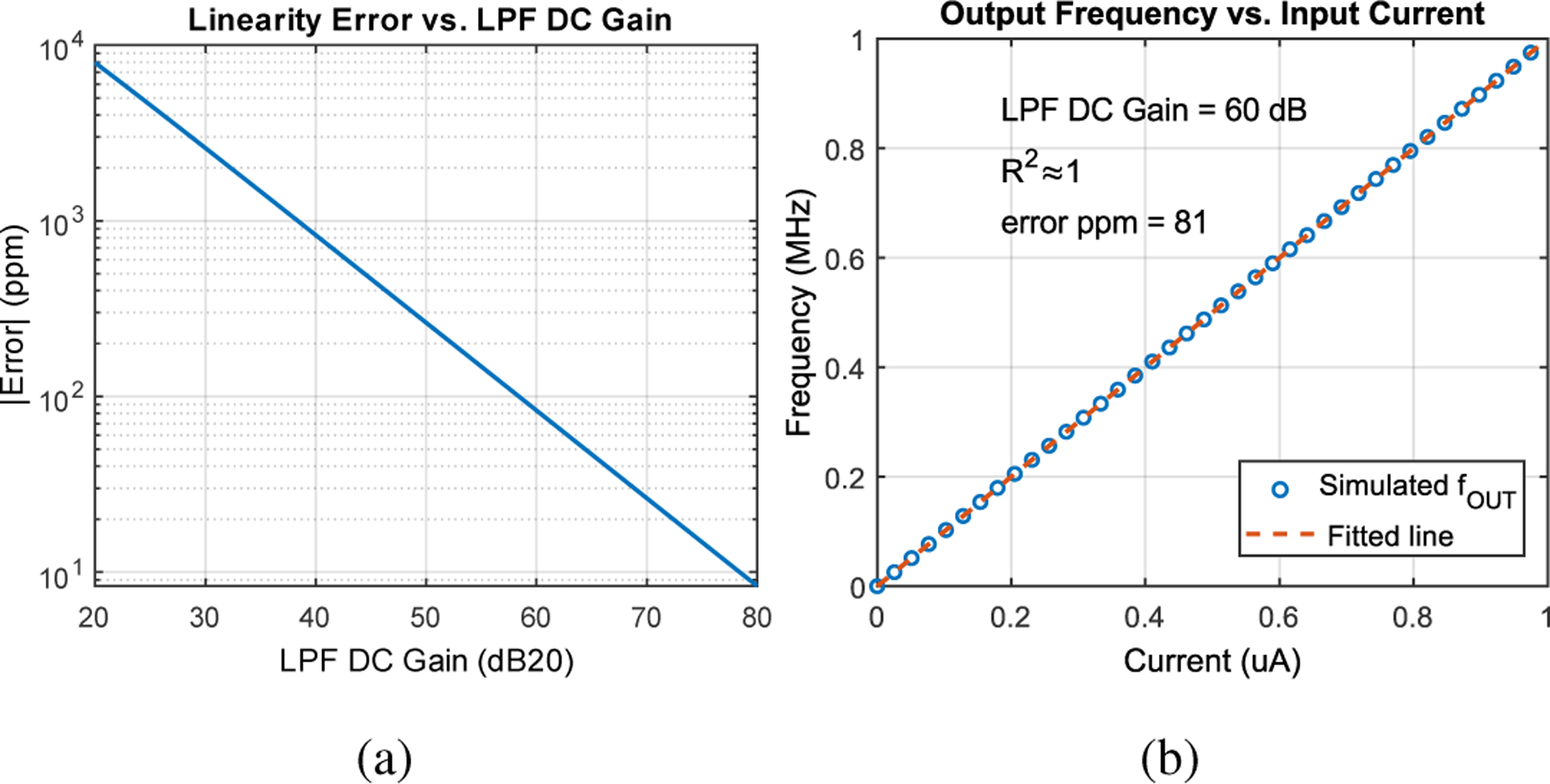
(a) MATLAB simulated linearity error vs. LPF DC gain. (b) MATLAB simulated frequency vs. current transfer curve for a 60dB LPF DC gain.
Based on (4), the FLL can also be used as a voltage-to-period converter if a constant reference current is sourced into and is used as a voltage-mode input. In this case,
| (5) |
and high linearity can be achieved. Furthermore, by using an op-amp structure with high input impedance, this high input impedance of the readout circuit is presented to the transducer output. As such, the FLL can interface with pH probe directly, which has a typical source resistance in the GΩ range, for voltage-mode sensing.
Because of the use of a switched capacitor in the feedback path, voltage ripples caused by capacitor charging and discharging, as well as voltage glitching caused by switch charge-injection, are present at the LPF input. However, these unwanted switching artifacts do not degrade overall readout performance for the following two reasons: first, any voltage ripple or glitching at the OPAMP input are low-pass filtered by both and the LPF; second, the switching frequency is at the frequency of the VCO, which is much higher compared to the signal bandwidth of interest.
III. Circuit Dynamic Analysis
In this section, more rigorous analyses of the loop dynamic of the FLL and small-signal transfer functions of the three measurement modes are provided. As it will be shown, because the FLL feedback is through the equivalent resistance of the switched capacitor, the transfer function of the feedback path is not constant. In other words, the s-domain transfer function of the circuit is dependent on the large-signal operating condition of the loop, including the values of and . This observation should be kept in mind when analyzing and designing the FLL, especially in current-mode and voltage-mode operation, where a larger VCO frequency range is used.
A. Resistance-to-Period Mode
Without considering the two LDOs that supply the top and bottom voltage supply rails of the WhB, the FLL is similar to [17], and its loop analysis is identical. Therefore, for brevity, we reiterate only the key conclusions of the derivation and provide slight clarifications.
First, we define the input differential voltage of the LPF, which is the difference between the positive and negative inputs, as . Under steady-state condition, the WhB is balanced such that , where is the resistance of the thermistor. Then, the WhB can be expressed using these two linearized s-domain transfer functions, as it translates both and to :
| (6) |
| (7) |
Note that in both transfer functions above, the term and appear. Therefore, the DC gain and the pole frequency of each transfer function ultimately change with respect to thermistor resistance and temperature. Provided that the thermistor has sensitivity , transfer function of the LPF is , and the VCO provides voltage-to-frequency gain , then the linearized small signal block diagram of FLL for resistance-to-period conversion can be drawn as shown in Fig. 4(a). Based on this, the loop gain of the FLL is
| (8) |
where and are the DC gain and dominant pole of the LPF, respectively. is the ratio of and . The loop transfer function is a two-pole system, and in our design we choose to use as the dominant pole frequency. Given a thermistor sensitivity parameter , the overall s-domain signal transfer function (STF) from temperature to period is
| (9) |
Fig. 4:
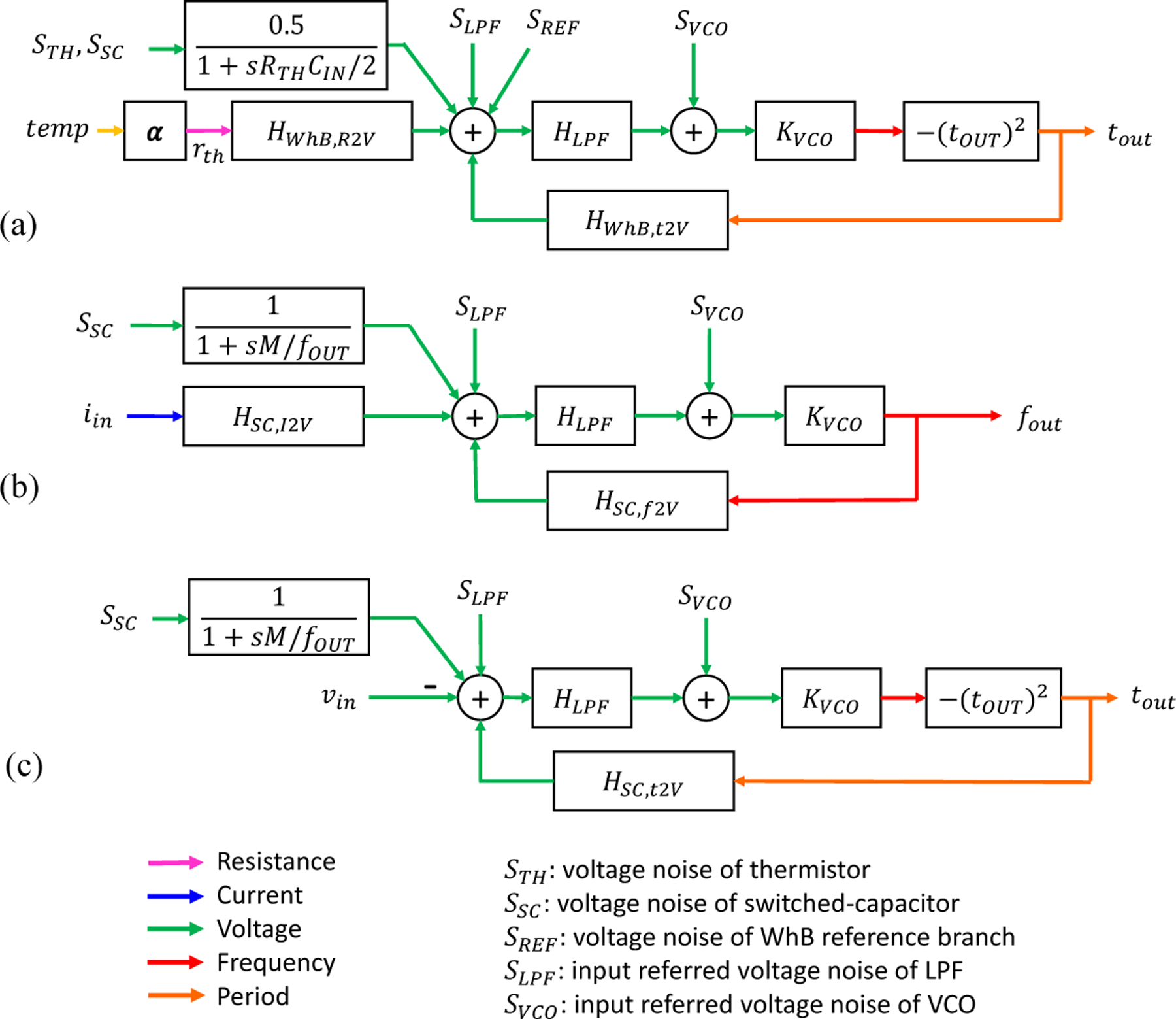
Small-signal block diagrams for (a) resistance-to-period, (b) current-to-frequency, and (c) voltage-to-period modes.
This readout circuit is designed for measuring the resistance of an off-chip commercial thermistor whose nominal resistance is 100 kΩ. If the top rail of the WhB is connected directly to supply, more than 10 μA of current is drawn and exceeds our power budget. As such, in order to limit or adjust power consumption, the top and bottom supply rail voltages of the WhB are set by voltage regulators. Decreasing the rail voltage difference of the WhB will reduce the temperature resolution of the readout circuit but theoretically leave the FoM unchanged [17]. However, practically speaking, adding voltage regulators will introduce additional noise to the WhB, further degrading resolution. Because of the WhB structure, this LDO noise can be mitigated or canceled if the transfer functions from top (or bottom) rail to nodes A and B are nearly identical across the bandwidth of interest. However, in order to achieve this, the noise from the reference branch resistors can no longer be band-limited. A second method is to simply place large decoupling capacitors at outputs of the LDO and at the reference branch output, but this requires additional bond pads for off-chip components. In this design, the first method is used to keep power consumption low, and the dominant noise source will be the reference branch resistors.
B. Current-to-Frequency Mode
Next we analyze the steady-state loop dynamic of the current-to-frequency mode of operation. Similar to the resistance-to-period mode, the SC network acts in both the signal path and the feedback path. In the signal path, the input current flows into the SC and generates a voltage. Assuming the FLL is locked, the small-signal current-to-voltage relation of the SC network can then be described as
| (10) |
In the feedback path, the SC network generates a voltage that is inversely proportional to the VCO output frequency. Therefore, the small-signal frequency-to-voltage relation of the SC network is
| (11) |
The linearized small signal block diagram of the system can be drawn as in Fig. 4(b). The loop gain of the FLL is
| (12) |
Equation (12) shows that both the DC gain and the second pole location vary across current operating conditions. This signifies two points of caution when designing the FLL: firstly, the input needs to maintain some minimum amount of current in order for the loop to operate safely; secondly, circuit blocks should be designed such that the loop is stable across the designed operating range. In our design, a constant offset current of 250 nA is injected to the SC. is designed to be 1 pF and , such that at . The LPF DC gain .
Loop DC gain and phase margin (PM) versus input current based on MATLAB calculation are plotted in Fig. 5(a). Loop stability worsens when the input current is low, caused by the fact that as FLL frequency decreases, the DC gain of the loop increases. Moreover, the second pole of the loop, which is dependent on the equivalent resistance of the SC, also reduces. In this design, the FLL is designed such that the minimum PM is above 45 degrees.
Fig. 5:
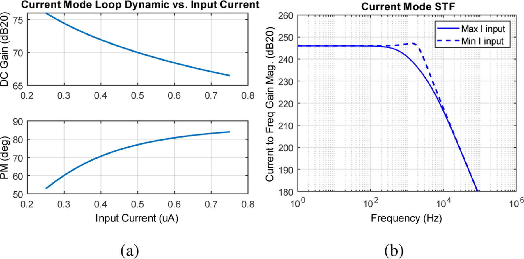
MATLAB simulated (a) current mode loop DC gain and PM and (b) current mode STF curves using actual design specifications
Based on the small-signal block diagram shown in Fig. 4(b), the s-domain STF from input current to output frequency is
| (13) |
At DC, the magnitude of is large, and the STF can be approximated as ; this agrees with the large-signal relationship derived in Section II. The magnitude of STF for (maximum input) and 250 nA (minimum input) are plotted in Fig. 5(b). Because the SC network also filters the input current, the input signal is second-order low-pass filtered before reaching the input of the VCO. The bandwidth of the STF is set by the unity gain bandwidth (UGBW) of the loop. Effectively, the FLL readout circuit filters the input signal before it reaches the VCO quantizer and alleviates the need for additional anti-alias filtering.
There are three main noise sources in the FLL circuits, and they can be identified as the voltage noise power of the SC, , the input-referred voltage noise power of the LPF, , and the input-referred voltage noise power of the VCO, . The noise transfer functions (NTF) from these noise sources to the output are
| (14) |
| (15) |
| (16) |
Similar to loop gain, as the large-signal operating condition changes, the magnitude and phase of the NTF also vary. For illustration, Fig. 6 shows the Bode plot of NTF magnitudes, simulated (MATLAB) using previously defined circuit specifications. The dashed lines are from , whereas the solid lines are from . One can observe that the NTFs all have higher magnitude when the input current is higher. Because the VCO is placed after the LPF, which has high gain near DC, the phase noise of the VCO is firstorder high-pass filtered by the loop. As a result, the phase noise requirement of the VCO is relaxed. This also mitigates the effect of VCO phase noise on long-term drift. Given that chip-to-chip variation in VCO frequency offset, voltage-to-frequency gain , and related parameters will be fixed for each chip after fabrication, with negligible phase noise contribution the remaining drift will typically be caused by changes in temperature. While the closed-loop FLL architecture is inherently temperature insensitive, this is further analyzed in Sec. V measurements.
Fig. 6:
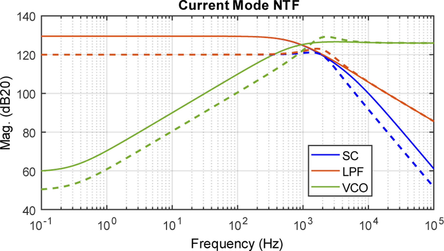
Current-mode NTF magnitudes for maximum input current of 750 nA (solid lines) and minimum input current of 250 nA (dashed lines).
C. Voltage-to-Period Mode
In this mode, because the output period of the VCO is proportional to input voltage, it is more intuitive to consider the switched capacitor as feedback translating oscillation period to voltage. In contrast to resistance-to-period mode, the error voltage is generated not from the voltage divider but from a reference current sourcing into the SC. Thus, the SC s-domain transfer function is
| (17) |
where is the magnitude of the reference current, which is set to 250 nA in this design. In the signal path, voltage output from the sensor directly connects to the negative input terminal of the LPF. The small-signal block diagram of the system is shown in Fig. 4(c).
The small-signal transfer function of the loop is identical to that of current-to-frequency mode. This is expected, since the physical feedback mechanism through the SC remains the same. However, since the current injected into the SC is now fixed, and the output of interest is oscillation period, it is more meaningful to write the loop transfer function as
| (18) |
Similar to the previous operating modes, the loop dynamic varies significantly across the operation range. For instance, we aim to have a voltage range of o.2 V to 0.6 V, and the calculated DC gain and PM of the loop are shown in Fig. 7(a).
Fig. 7:
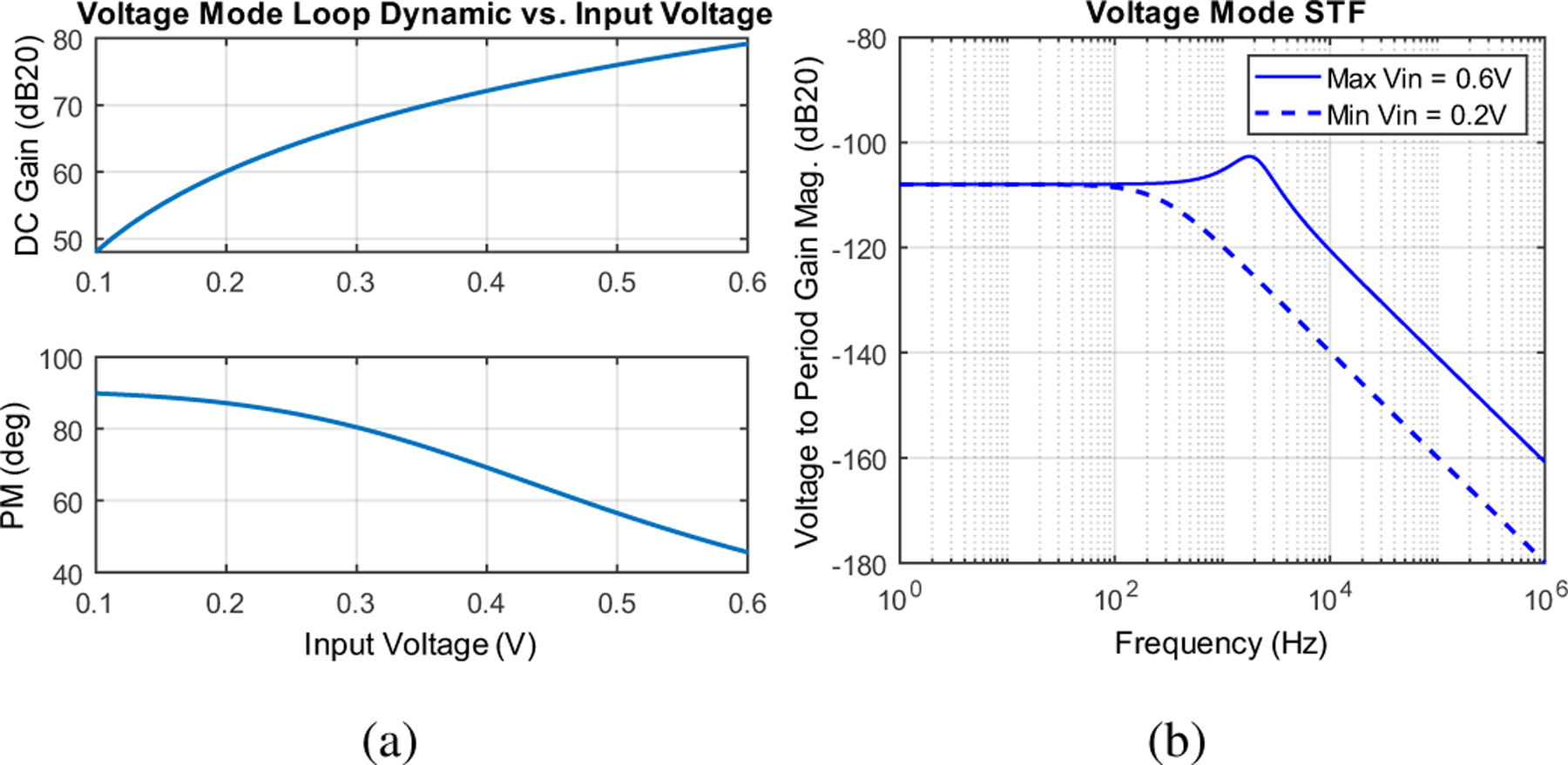
Simulated (a) voltage-mode loop DC gain and PM, and (b) voltage-mode STF curves.
The STF of voltage-to-period conversion is derived as
| (19) |
At low frequency, the STF is approximately , which agrees with the large-signal derivation. Fig. 7(b) plots the magnitude of STF for and 0.6 V. The noise analysis for voltage-mode operation yields same NTFs as for current-mode operation.
D. Design Considerations
This section has shown that using an FLL-based approach for tri-mode sensing introduces particular challenges. Given a STF bandwidth requirement, the first step in the design process is to determine the loop UGBW specification. From a stability point of view, the second pole of the FLL, which is formed by the input capacitor and the equivalent resistance of the SC, should be placed higher than the UGBW of the loop to ensure safe PM. Because the location of the second pole is set by , where typically for incomplete settling of the SC, a larger UGBW requires a higher second pole frequency, thus requiring higher VCO frequency in turn. In all three FLL configurations, stability is most marginal when VCO frequency is low. On the other hand, because the loop DC gain also changes with respect to input, the closed-loop linearity of the system can also degrade slightly if the VCO frequency is too high.
Among all noise sources, the switched capacitor noise power, which is proportional to its equivalent resistance , is unavoidable and coupled to the operation of the loop. To reduce this noise contribution, a larger or higher FLL frequency is required, which increases either circuit area and power. To maintain a feasible common-mode input range to the LPF, the current magnitude sourced to the should also be scaled accordingly.
For current- and voltage-mode operation, and set the large-signal current-to-frequency gain and voltage-to-period gain, respectively. In current mode, is used as an offset current to keep the loop stable, and its inaccuracy will cause a fixed output frequency offset. In general, slight variations in and will mostly result in gain error and offset error, as seen in (4)-(5), which can be compensated by calibration. While these references do affect the small-signal response of the circuit, the circuit itself should be designed to be robust enough such that minor variations in loop gain are not detrimental.
IV. Circuit Design Details
A. Reconfigurable Feedback Network
The high-level schematic of the proposed FLL-based sensor system is shown in Fig. 8. In resistance measurement mode, the feedback network is a WhB whose top and bottom rail voltages are set by a pair of low-dropout (LDO) voltage regulators. The right leg of the WhB is formed by an off-chip thermistor and an on-chip switched capacitor, . The off-chip thermistor (TI TMP63) used for this design has a nominal resistance of 100 kΩ and a sensitivity of 6400 ppm/°C. To satisfy the bandwidth requirement of the STF, the capacitance of the SC, , is 10 pF to provide an equivalent resistance of 100 kΩ at 1 MHz FLL output frequency. To create incomplete settling, on node A is ~500 pF, which supplies the instantaneous charging of . 450 pF of is supplied by an off-chip capacitor, , to save die area. This ratio of 50 ensures that the SC equivalent resistance is linearly dependent on switching period. Because incomplete settling does not require an accurate capacitance value, parasitic capacitance on node A has minimal effect in linearity, including the additional loading from bond pad and packaging stemming from the off-chip . The inductance resulting from the bound wire is in the nH range, and its effect is negligible at MHz switching frequency. Thus, this WhB architecture is well suited for interfacing with an off-chip thermistor.
Fig. 8:
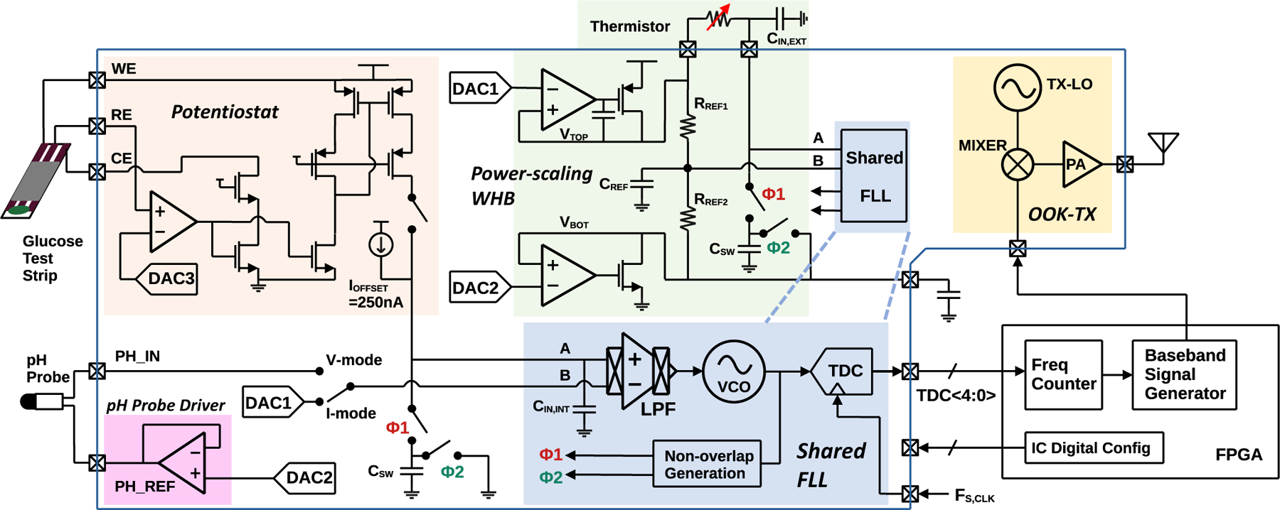
Top level schematic.
On the left WhB leg, two 1 MΩ polysilicon resistors are used to generate a reference voltage at node B. The two voltage regulators are designed to operate at low power, and as such their noise is significantly higher than the resistor thermal noise. If the WhB is balanced, however, the transfer functions from regulator output ( or ) to node A and node B are identical, and the regulator noise will appear as common mode at the LPF input and be canceled. However, in order to achieve equal transfer function across the signal bandwidth of interest, the thermal noise of the reference resistors cannot be band-limited with a large capacitance. As such, a capacitor of 50 pF is also placed at node B such that the pole frequencies of node A and B are approximately the same. Because of this, the noise from the reference resistors will dominate the thermal noise of the WhB, relaxing noise requirements for the regulators and enabling a more power efficient LDO design. For results shown, the top regulator sets the top WhB voltage supply rail to 0.675 V and uses Miller compensation. The bottom regulator sets the bottom voltage supply rail to 0.45 V. As its output sees significant ripple from the discharging, it is beneficial to connect a large capacitor to ground to attenuate the ripple and to set the dominant pole.
When the FLL is configured for current- or voltage-mode, the WhB voltage regulators and reference branch are disabled and disconnected to save power. To accommodate the desired input signal range and to keep the VCO frequency below 1.5 MHz, is digitally adjusted to 1 pF and is reduced to 50 pF. Since the SC is made from an array of capacitors that are digitally selectable with NMOS switches, the on-resistance of the switches is designed to be less than 2 kΩ so that it does not affect the accuracy of SC equivalent resistance.
B. LPF and VCO Quantizer
The active low-pass filter (LPF) was designed using a two-stage op-amp, such that at a low supply voltage of 1.2 V it has enough output voltage swing to control the VCO. The op-amp DC gain is 70 dB to achieve high FLL linearity and to attenuate VCO flicker noise. The LPF sets the FLL dominant pole, which critically affects loop stability. As such, Miller compensation with nulling resistor is used, and a Miller capacitor of 16.1 pF is needed to create a pole at 0.5 Hz. Chopping ensures that thermal noise dominates the total noise floor; the chopping clock is generated from the VCO output using a 1:4 clock divider. To provide adjustability in case of PVT variation, the LPF DC gain can be adjusted down by 6 dB, and its nulling resistor can be digitally trimmed.
The VCO consists of a source-follower-based transconductance stage and a current controlled oscillator (CCO), as shown in Fig. 9. The CCO has 5 delay stages that use a constant energy-per-cycle (CERO) topology [24]. There are two major sources of nonlinearity. First, the voltage-to-current relationship of the transconductor is not exactly linear, since the source degeneration resistor only moderately linearizes the voltage-to-current gain. Second, the starvation current in the delay stages is not an exact copy of the transconductor current. Although as previously shown, variation of does not affect the large-signal relationship between the FLL input and output frequency, it still changes the loop gain, affecting the small-signal characteristic of the loop. Therefore, it is prudent to maintain a relatively constant for robust stability. In addition, under PVT variation, higher can undermine loop stability, whereas significantly lower could cause the LPF to be swing-limited. As a result, the source degeneration resistor is made adjustable to cover possible gain variations. Fig. 10 shows the simulated VCO tuning curve under different settings; in nominal condition, is configured to be 2 MHz/V. Because of the use of PMOS current mirror for generating current starvation, the VCO itself has poor power supply rejection. When the VCO is placed in the FLL, the feedback offers power supply rejection at low frequencies where the loop gain is high. However, high frequency supply noise cannot be suppressed in this proof-of-concept design.
Fig. 9:
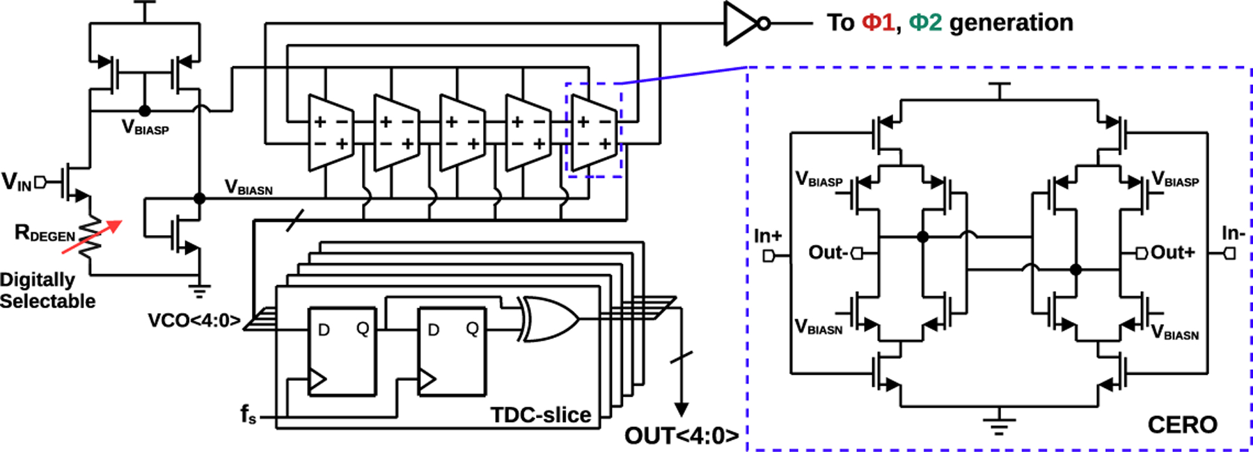
5-stage VCO and TDC for sampling VCO frequency.
Fig. 10:
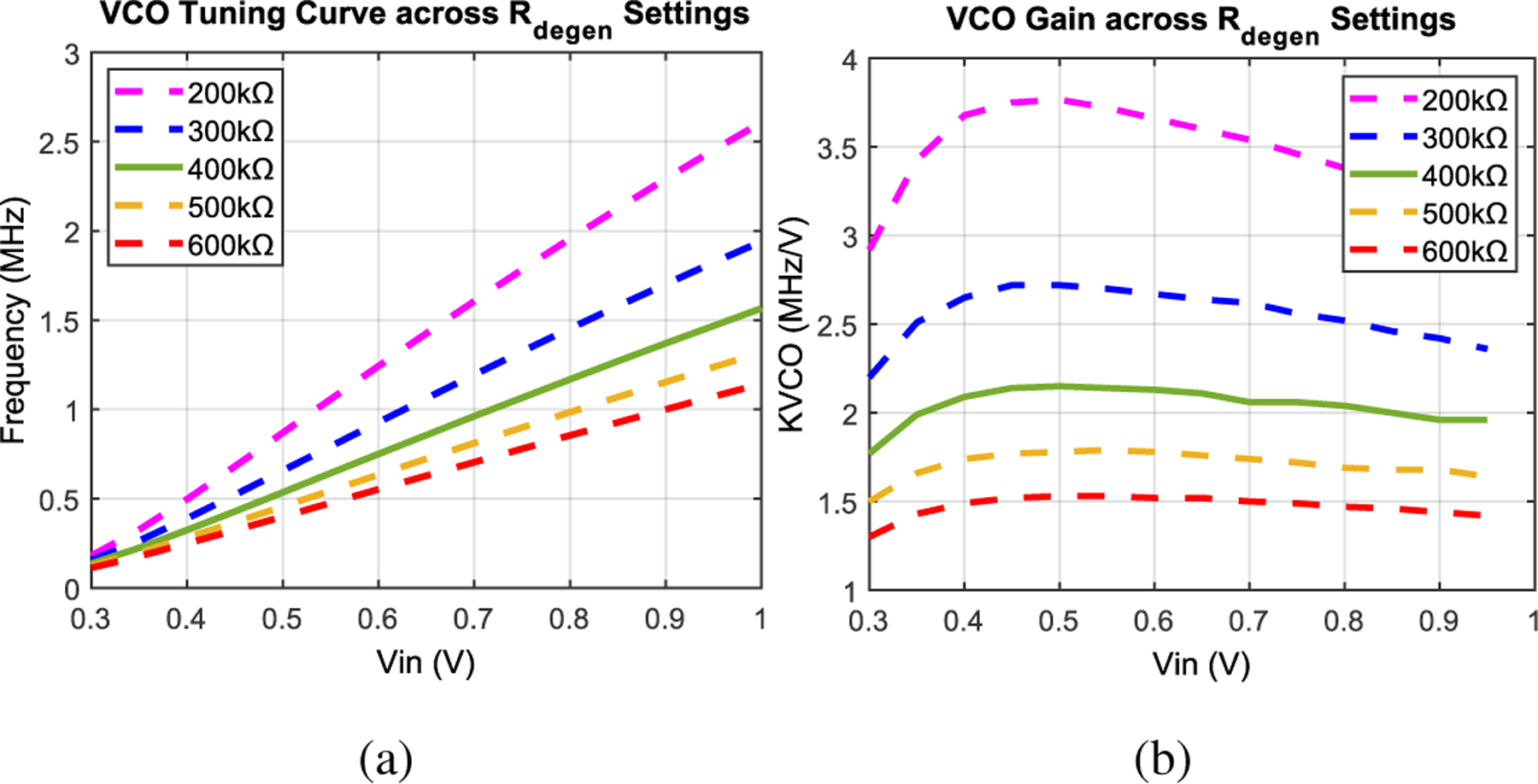
(a) VCO tuning curves and (b) VCO gain with different degeneration resistor values, simulated from transistor-level designs.
The outputs of delay stages connect to a time-to-digital converter (TDC) that oversamples the phase, an efficient high resolution architecture amenable to process scaling [19]. Frequency is extracted through the subtraction operation of two consecutive samples. This effective differentiation operation provides first-order quantization noise shaping. Because the maximum VCO frequency is designed to be 1.5 MHz, the D-flipflops are clocked at 3 MHz. In this design, the total noise is not limited by the quantization noise.
C. Potentiostat and Supporting Analog Circuits
To enable current-mode electrochemical measurements, a three-terminal potentiostat was also implemented on chip [25]. The working electrode (WE) terminal is connected to the voltage supply rail, and the current of interest flows into the counter electrode (CE) input. A bulk-driven, high-gain op-amp creates a feedback loop such that the voltage at the reference electrode (RE) is equal to the output of an on-chip DAC. In order to measure current ranges that are relevant for common glucose and lactate sensors (1–10 μA), a current mirror ratio of at least 20:1 is needed to convey the output current of the potentiostat to the input of the current-mode configured FLL. As implemented (400:1), attenuation is higher than necessary and causes degraded current sensitivity. As such, performance can be further improved in future implementations.
As the allowable input voltage range of the FLL during voltage-mode operation is limited to 0.2–0.6 V, an on-chip voltage buffer is used to drive the negative terminal of an off-chip pH probe to a set reference voltage, and the positive terminal of the pH probe then connects to the FLL input at node B. For voltage reference generation, three 4-bit R-string DACs are included on-chip.
D. Wireless Transmitter
An on-chip transmitter using an on-off keying (OOK) modulation scheme is used to demonstrate a wireless sensor system. It utilizes the 13 MHz frequency standard for Near Field Communication (NFC), because the readout system does not have a high data rate requirement and is compatible with commercial, off-the-shelf NFC antennas. The IC includes a 13 MHz ring oscillator and a power amplifier (PA). An off-chip LC matching network matches the PA pad to a commercial coil antenna. Because of the low data rate needed for temperature and pH measurements and chronoamperometry, the transmitter only needs to intermittently transmit data. Thus, the power amplifier is duty-cycled by controlling the baseband signal sequence, which contains the serialized count of FLL frequency. For proof-of-principle and flexibility during testing, a frequency counter and baseband signal generator are implemented off-chip using an FPGA; in future implementations, this simple logic can be implemented on-chip at low power for automated TX duty-cycling.
V. Measurement Results
A prototype IC was fabricated using a 0.18μm CMOS process (Fig. 11) and operates at 1.2 V supply voltage. The active circuit area, excluding the TX, is 0.5 mm2. For electrical characterization, the output of the TDC, sampled by a 3 MHz clock, was collected by a logic analyzer, and counting and spectral analysis were performed in MATLAB. For measurements that require collecting long periods of data, a bench-top frequency counter (Tektronix FCA3000) or FPGA module (Opal Kelley XEM7310) was used to record the VCO frequency or period.
Fig. 11:
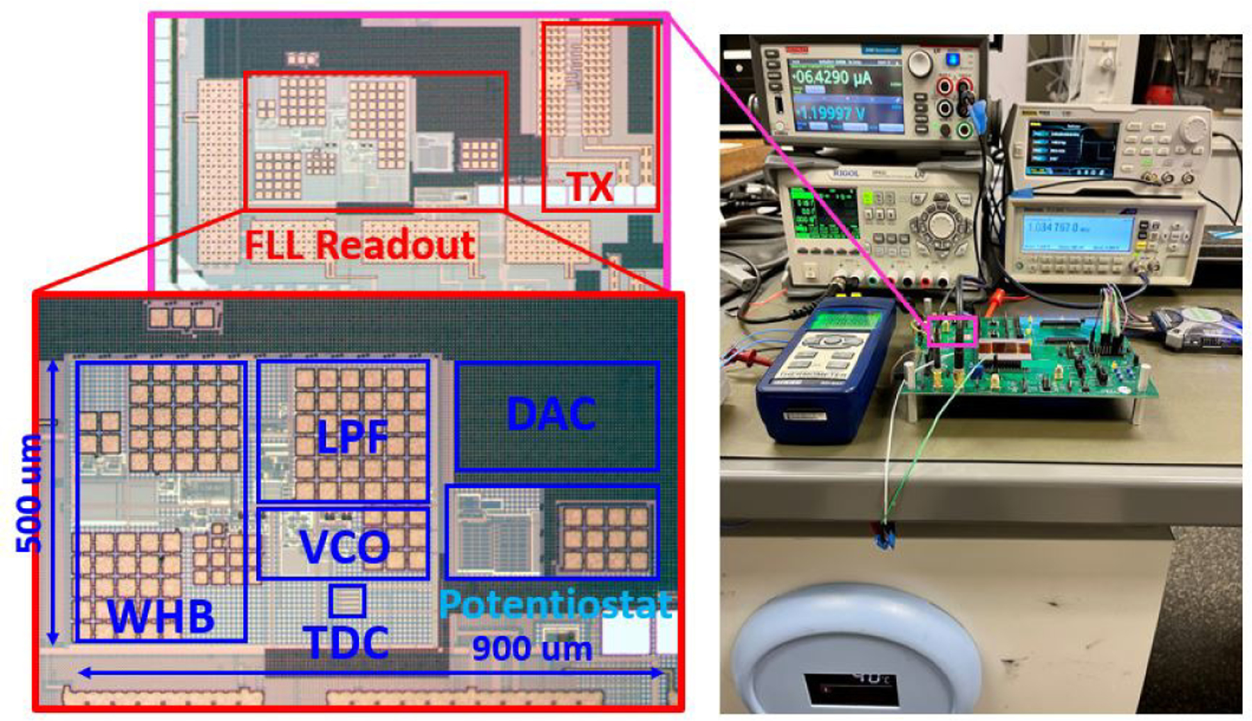
Die photo and experimental test setup.
A. Resistance-mode and Temperature Measurement:
The resistance-to-period operation mode was first characterized using an off-chip potentiometer. Fig. 12(a) verifies the high linearity of the conversion across three separate IC dice. To quantify minimum resistance resolution, the TDC output was recorded, and the resulting power spectral density (PSD) is shown in Fig. 12(b). For 100 Hz bandwidth, the resistance resolution based on integrated RMS noise is 10.5 Ω. Interfacing with the selected off-chip thermistor (TI TMP63), the equivalent achievable temperature resolution is 16.4 mK. Fig. 12(c) shows the power consumption of the readout circuit versus input resistance. In nominal condition, with a test resistance of 100 kΩ, measured power consumption including the WhB is 9.2 μW; simulated power breakdown of individual circuit blocks is shown in Fig. 12(d).
Fig. 12:
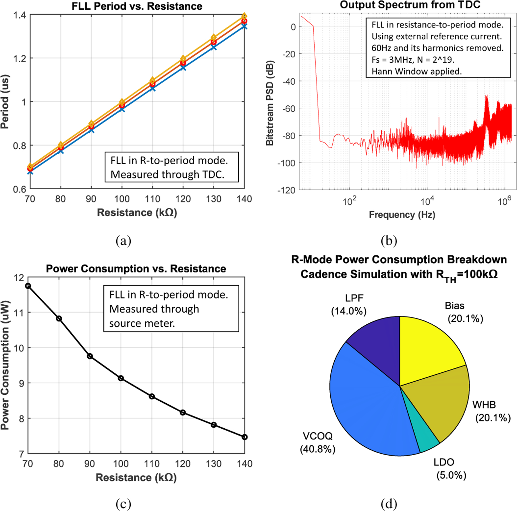
(a) Resistance-to-period transfer curve measured using a reference potentiometer across three chips. (b) PSD of the TDC output. (c) Measured power consumption vs. input resistance. (d) Simulation power breakdown.
For demonstrating temperature measurement, the readout circuit was interfaced with an off-chip thermistor (TI TMP63), and the thermistor was placed in an oven or cold bath, with the IC at room temperature.This experimental setup is representative of use cases in which the thermistor and IC are at different temperatures, common for temperature probe (i.e. digital thermometer) applications; this also allows standalone characterization of read-out as a function of off-chip thermistor temperature separate from IC temperature variation. Fig. 13(a) shows the measured period of the VCO with respect to thermistor temperature. The temperature gap around 15°C is because neither test environment generates a stable temperature within this range, and the slight nonlinearity stems from the thermistor itself, as verified by the datasheet and in contrast to Fig. 12(a). We demonstrate a linear operational range from 0°C to near 80°C. While our experimental setup is unable to provide stable, dry testing conditions below 0°C, in practice, based on the actual resistance measurement range of the FLL as shown in Fig. 12, the temperature measurement range would cover at least −25°C to 80°C for interfacing with the TMP63 thermistor. Ultimately, the temperature range and resolution will depend on the off-chip thermistor used for temperature measurement. For instance, a thermistor with a similar nominal resistance but smaller temperature sensitivity will result in a larger measurable temperature range but with worse temperature resolution.
Fig. 13:
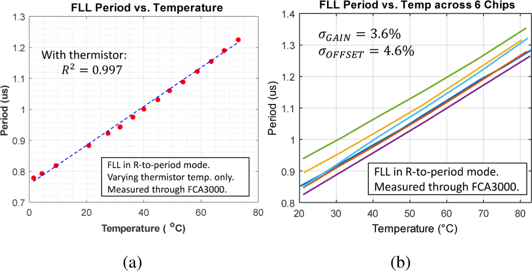
Measured temperature transfer curve with off-chip thermistor for a (a) single chip and (b) across 6 chips.
In addition, a temperature sweep was performed across six different ICs to assess the variation among chips. In this series of tests, both the thermistor and the IC were placed inside an oven, in part to represent use cases in which the off-chip thermistor and IC are co-located and at the same temperature, as well as to capture maximum variation of the complete system across temperature. As seen in Fig. 13(b), different dice manifest small variability in both gain slope and offset, which is likely due to process variation of the WhB. Based on the data shown in Fig. 13(b), we are able to calculate the standard deviation of gain and offset for these dice, following a two-point calibration at 30 and 68 degrees; the standard deviation in gain is 3.65%, and the standard deviation in offset is 4.6%. Because of the long time intervals needed in order to let the temperature stabilize in the oven, an external frequency counter is used to more feasibly monitor that the VCO period has stabilized. Thus, period data collected for Fig. 13 is from the external frequency counter instead of the on-chip TDC.
B. Current-mode and Potentiostat Measurement:
To demonstrate the FLL configured as a current-to-frequency converter along with the integrated functionality of the on-chip potentiostat, measured frequency vs. current transfer curves from three chips are shown in Fig. 14(a). In this measurement, the input current of the potentiostat was swept from below 1 μA to 200 μA by controlling the RE voltage and the resistance between RE and WE terminals; good linearity is obtained. When the potentiostat input current exceeds ~200 μA, current mirror devices that interface between the potentiostat and the FLL begin to enter the triode region, causing nonlinearity. We note that this 0–200 μA measurement is performed to test the designed FLL input dynamic range of 0–500 nA, since a fixed mirroring ratio of 400:1 was implemented between the potentiostat and the FLL input. In practice, the system as implemented is designed to measure currents within 0–100 μA, and electrochemical measurements will typically be in the tens of microamps range (e.g. glucose test strips). If variable current scaling is implemented in a future implementation, as done in [1], the input dynamic range of the cascaded system can be further improved.
Fig. 14:
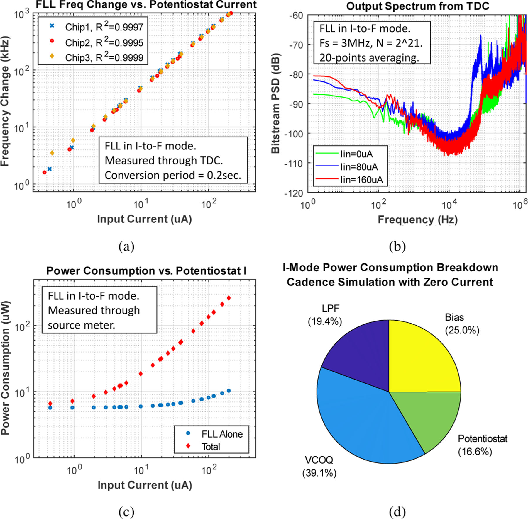
(a) Measured current-to-frequency transfer curves from three chips. (b) PSD of the TDC output. (c) Measured power consumption vs. potentiostat input current. (d) Simulation power consumption breakdown with zero potentiostat current
Fig. 14 (b) shows the TDC output spectrum with DC current magnitudes of 0 μA, 80 μA, and 160 μA at the potentiostat input. The purpose of showing the spectra for three different input levels is to verify our previous analysis, in which the output-referred noise of the system increases with input. Indeed, for a 100 Hz bandwidth, the RMS current noise, referred to the FLL input, is 40.6 pA for 0 μA input, and 69.3 pA for 160 μA input. The difference in the low-pass corner frequency of the noise spectrum can also be observed between the three curves, which is due to the movement of second pole location of the loop, as predicted in (12). Because chopping is not implemented in the potentiostat, a flicker noise component can be seen at the FLL output, and becomes more prominent with increasing input current.
The measured power consumption of the readout circuit with and without potentiostat power is shown in Fig. 14(c). In current-mode operation, overall power consumption of the IC with the potentiostat idle is 6 μW. Whereas when a large amount of current is pushed from VDD into the potentiostat, and thereby into an external device under test, total power consumption of the system will be dominated by this reaction current, which is dissipated by the DUT and not consumed by the potentiostat. The simulated power breakdown during idle is shown in Fig. 14(d) .
As a further proof-of-concept, a series of glucose chronoamperometry measurements was performed. Fig. 15(a) shows the test setup. For each measurement, a commercial glucose test strip was connected to the terminals of the potentiostat. Droplets of prepared β-D-glucose solution were added to the test strip, with a quiet time of 10 seconds at 0 V applied between the WE and RE. Subsequently, a voltage step of 200 mV was applied between the WE and RE to begin the reaction. Frequency data were collected using a FPGA at a 100 Hz sampling rate. Fig. 15(b) superimposes the transient responses of the glucose sensor measured via FLL readout for concentrations from 2.5 mmol/L to 50 mmol/L. The response frequency is demonstrably proportional to sample glucose concentration. Because of the large fixed attenuation ratio of 400 between the potentiostat output and the FLL, the higher concentration values for this test exceed the clinically relevant range to demonstrate the dynamic range of the FLL.
Fig. 15:
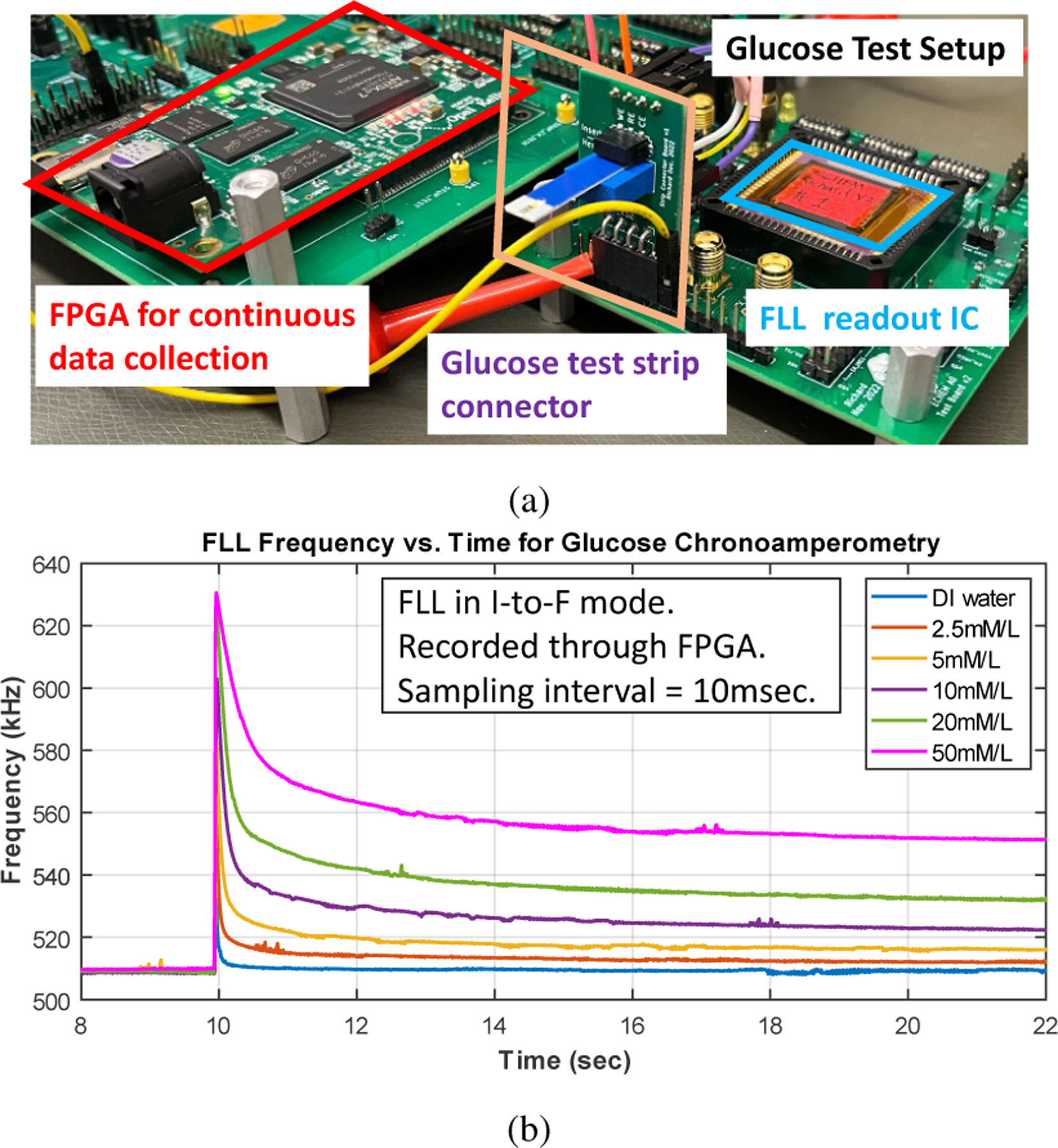
(a) Photo of test setup for glucose chronoamperometry, and (b) measured transient frequency outputs.
C. Voltage-mode and pH Measurement:
Voltage-to-period mode was first characterized by sweeping the input voltage and measuring the resulting output period. As shown in Fig. 16(a), a highly linear relationship was obtained within the designed input range of 0.2 0.6 V. In theory, according to (4), the output period versus voltage slope should be 4 μs/v as dictated by the values of and . However, slightly higher slopes are observed in this measurement likely due to higher compared to ideal. The power consumption of the readout circuit versus input voltage is shown in Fig. 16(b). As input voltage increases, the oscillation period of the VCO decreases, thus reducing the overall power consumption. Fig. 16(c) illustrates the PSD of the TDC bitstream, measured at 200 mV, 400 mV, and 600 mV for input . Because the PSD is a representation of noise in the frequency domain, this group of curves confirms our previous analysis; when the FLL output frequency is lower, the output-referred frequency domain noise is also lower. For 100 Hz bandwidth, the input-referred RMS voltage noise is between 31.7 μV and 81.9 μV. In addition, the noise roll-off at around 2 kHz is due to the pole locations of the NTFs. The peaking from the 600 mV curve indicates the phase margin of the loop becomes degraded at higher input voltage.
Fig. 16:
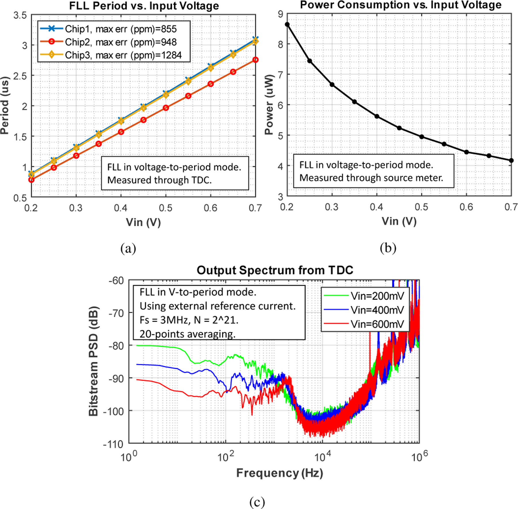
(a) Measured voltage-to-period transfer curves from 3 chips. (b) Measured power consumption vs. input voltage. (c) TDC output spectrum.
To demonstrate voltage-mode operation using a relevant sensor, pH measurement was demonstrated using an off-chip pH probe. The integrated OOK transmitter (TX) was also used to demonstrate wireless sensor operation. The test setup is shown in Fig. 17(a). The voltage input of the FLL is connected to a commercial pH probe (Oakton 59001–65) at its positive terminal, and the pH probe is placed in different pH calibration buffer solutions sequentially. An FPGA is used for IC configuration, frequency counting, and baseband signal generation. OOK transmission is enabled every 1 ms to transmit a 12-bit number representing the measured output frequency of the FLL. The data rate is set to 100 kb/s. On the receiver side, following a discrete amplifier and band-pass filter, data is captured using an oscilloscope. Bit detection is perform through square law demodulation in MATLAB. Fig. 17(b) shows that the FLL linearly converts pH value to period between the pH range of 1.6 to 12 .
Fig. 17:
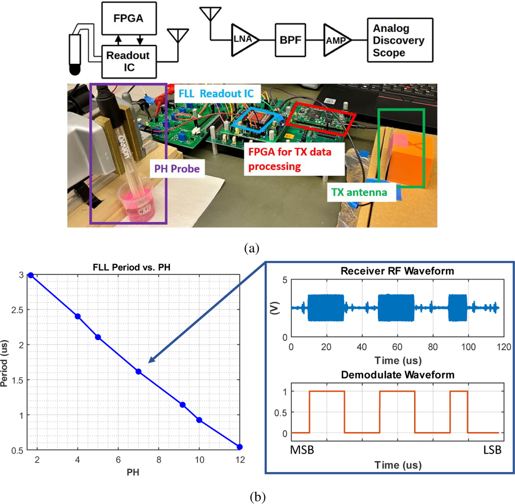
(a) Setup for performing pH measurement as a wireless sensor, and (b) measured period versus pH result based on demodulated the receiver signal.
D. Calibration:
The measurement results of the previous three subsections show the digitized FLL timing output with respect to temperature, glucose concentration, and pH. While the FLL-based readout is demonstrated to be highly linear, as quantified for each operational mode in Sec. V.A-C, calibration may be required for use as practical bio-instrumentation to account for variation or nonlinearity introduced by the off-chip transducer, as well as accounting for chip-to-chip gain and offset variations for the read-out IC (as in Fig. 13(b)). For temperature and pH sensors used in our experiment, a two-point linear calibration is generally sufficient. For example, Fig. 18 (a) and (c) show the the linear functions of temperature vs. period and pH vs. period after performing two-point calibration on the existing data. The maximum temperature error after calibration is 3°C, due to the inherent nonlinearity of the thermistor. And for pH, the maximum error from the fit line is 0.35 pH.
Fig. 18:
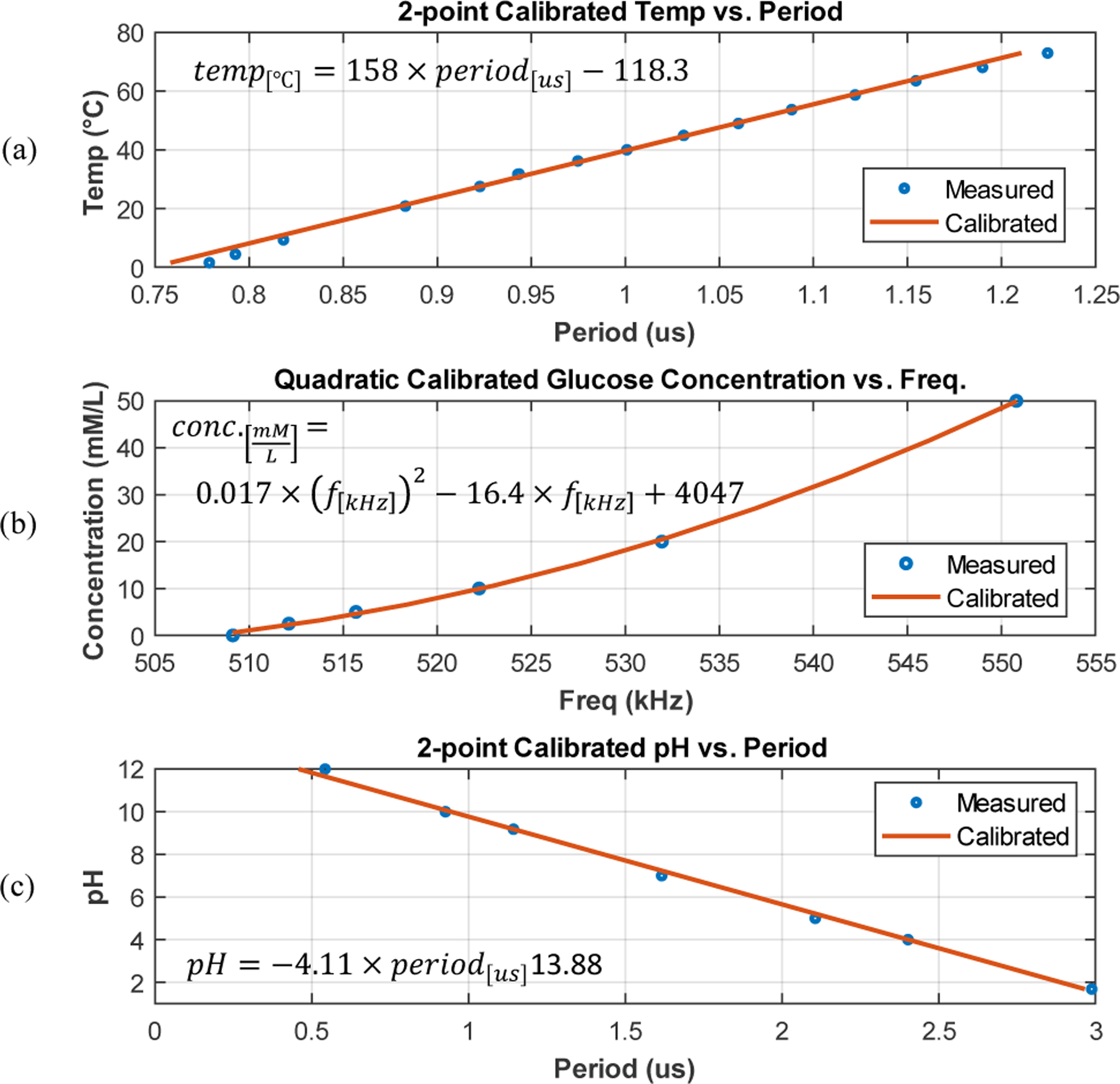
Calibrated transfer curves that can be used to back-calculate (a) temperature, (b) glucose, and (c) pH based on FLL period or frequency.
In the case of chronoamperometry, while current-mode operation of the FLL itself is linear (Fig. 14 (a)), the transducer output current after initial transient settling is not linearly proportional to glucose concentration due to the inherent characteristic of the glucose test strip. Instead, as shown in Fig. 18 (b), a quadratic fit can be used to accurately estimate the glucose concentration based on frequency, with a maximum error from the fit line of 0.6 mM/L. The use of alternative resistance-mode, current-mode, or voltage-mode sensors would require similar calibration approaches.
E. Performance Comparison
A more detailed comparison with recent related works is shown in Table I.
TABLE I:
Performance Comparison
| Ref. | [1] TBioCAS 2021 |
[12] JSSC 2019 |
[17] JSSC 2020 |
[14] BioCAS 2022 |
[13] ISCAS 2020 |
[26] ISSCC 2023 |
This Work |
|---|---|---|---|---|---|---|---|
|
Mode
(Sensor Target) |
I (Echem, Temp) |
I (Echem, Temp) |
R, C (Temp, RH) |
I, V (Echem, pH) |
I, V (Echem) |
I, V (Temp, Echem, pH) |
R, I, V (Temp, Echem, pH) |
| Active Area (mm2) | 8 | 0.01 | 0.72 | 0.037 | 0.098 | 2.51 | 0.52 |
| Processs (um) | 0.18 | 0.25 | 0.18 | 0.18 | 0.18 | 0.18 | 0.18 |
| Supply (V) | 1.2 | 2.5 | 1.5 to 2 | 1.2 | 1.4 | 1.8 | 1.2 |
| Power (μW) | 493 | 250 | 15.6 | 2.2 | 40 | 22 (peak) | R-mode: 9.24 I-mode: 65 V-mode: 5.66 |
| ADC Type | Relax Osc + TDC | ΔΣ ADC | VCO + TDC | Relax Osc | Incre. ADC | SAR | VCO + TDC |
| Communication | On-chip TC & TC | Wired | Wired | Wired and TX | Wired | Wired | Wired and TX |
| Amperiometric Sensing | |||||||
| Current Range | ±6μA | ±12.5nA | NA | 2μA | 0.1μA | ±10μA | FLL only: 0.5μA With PSTAT: 200μA |
| R2 Error | 0.995 | Unknown | NA | 0.999 | 0.998 | NA | >0.9995 |
| Input-Ref. Noise | 2pA BW=Unknown |
0.28PA BW=20Hz |
NA | Unknown | 44.6fA BW=Unknown |
14pA BW=16Hz |
40.6pA BW=100Hz7 |
| Pattern Gen. | On-chip analog | Off-chip | NA | On-chip 4-bit DAC | Off-chip | On-chip DAC | On-chip 4-bit DAC |
| Potentiostat | On-chip | Off-chip | NA | On-chip | NA | On-chip | On-chip |
| Voltage Sensing | |||||||
| Voltage Range (V) | NA | NA | NA | 0 to 1 | 0.32 to 1.05 | 0 to 1.8 | 0.2 to 0.6 |
| R2 Error | NA | NA | NA | 0.999 | 0.974 | 0.99999 | > 0.9999 |
| Input-Ref. Noise | NA | NA | NA | Unknown | 1.7μV BW=10kHz |
72.3μV BW=16Hz |
31.7μV BW=100Hz8 |
| pH Range | NA | NA | NA | 4 to 10 | NA | 4 to 10 | 1.6 to 12 |
| Temperature Sensing | |||||||
| Linear Range (°C) | 20 to 80 | 25 to 65 | −40 to 85 | NA | NA | Unknown | 0 to 759 |
| Resolution | 43mk BW=Unknown |
NA | 2mK BW=500Hz |
NA | NA | Unknown | 16.4mK BW=100Hz10 |
| Transducer | Ring oscillator | Diode | On-chip Poly-R | NA | NA | Unknown | Off-chip thermistor |
Estimated active readout circuit area only
FLL readout circuit active area only. Also requires off-chip capacitors
Includes pattern/clock generation
Thermistor at nominal resistance
Potentiostat idling
Mid-rail input voltage
With zero input current at FLL readout circuit input
At minimum input voltage
Based on TI TMP63 thermistor
In amperometric sensing, after taking power consumption into account, the proposed FLL topology is able to achieve competitive noise performance compared to relaxation oscillator-based [1] and TIA-based [26] approaches. Because adjustable current scaling [1], [26] is not implemented in this work, overall dynamic range is limited to 52 dB. However, this can be improved by including adjustable current mirror in future designs. The goal of our SoC is to demonstrate chronoamperometry, such as for glucose concentration readout, requiring only single-level voltage steps. As such, peripheral circuitry only includes a 4-bit voltage DAC to set the reaction voltage. While this does not support fast-scan cyclic voltammetry or square-wave voltammetry at this resolution, the core FLL-based readout can be readily applied in future systems that require more complicated sensing schemes.
For voltage measurement, the FLL readout circuit achieves improved noise performance compared to conventional low-noise amplifier and SAR architecture [26] at significantly lower power consumption. Additionally, voltage-mode linearity is superior to open-loop-based oscillator architectures [13], [14]. One shortcoming of the FLL is the limited input dynamic range, due to the stability constraint of the loop and VCO tuning range. Nevertheless, it still enables the system to cover the common pH probe voltage range when interfaced with a commercial pH probe.
For resistive temperature measurements, our circuit achieves this functionality with ~40% lower power consumption compared to [17] /(9.2 μW vs. 15.6 μW), largely at the cost of degraded temperature resolution inherent to power reduction. This resolution trade-off stems from two sources: to halve WhB power while also interfacing to a (~3X) smaller thermistor requires a 6X reduction in WhB voltage supply, as is shown in this work (300 mV vs. 1.5 V in [17]), with commensurate reduction of the signal-to-noise ratio (SNR) of the transducer Additionally, the noise of the WhB reference branch resistor is not bandlimited and dominates overall noise, which would require additional off-chip components to fully mitigate.
VI. Conclusion
In this work, a tri-mode, FLL-based readout circuit for resistance-, current-, and voltage-mode inputs was presented. It was integrated into a multimodal SoC with wireless TX capability for interfacing with off-chip temperature, electrochemical, and pH sensors. Compared with recent related works shown in Table I, the proposed readout circuit is capable of performing all three measurements without the need for additional active AFE interfaces, reducing analog circuitry overhead. Thanks to its closed-loop architecture, linearity performance is excellent for all three measurement modes. The lower power consumption of the FLL readout circuit improves the state-of-the-art, achieving <10μW read-out operation for each measurement mode, and makes it especially valuable for future ultra-low-power applications, such as wearable devices in health and medicine and power autonomous (i.e. batteryless) sensors. The VCO-based approach may also be scalable to advanced CMOS nodes, where implementation of highresolution ADCs is increasingly challenging at low voltage (<1 V) operation. While demonstrated here for temperature, pH, and amperometry, the core FLL-based readout approach can be extended to a variety of additional biological and chemical sensors in future work.
Acknowledgements
This work was supported in part by the Center for Design of Analog-Digital Integrated Circuits (CDADIC), and in part by the National Institutes of Health under awards R01EB028104 and R21DE031101.
Contributor Information
Siyuan Yu, School of Electrical Engineering and Computer Science, Oregon State University, Corvallis, OR 97331 USA..
Tzu-Hsuan Chou, School of Electrical Engineering and Computer Science, Oregon State University, Corvallis, OR 97331 USA..
Soumya Bose, chool of Electrical Engineering and Computer Science, Oregon State University, Corvallis, OR 97331 USA. He is now with Intel Labs, Hillsboro, OR 97124 USA..
Jacob Cook, School of Electrical Engineering and Computer Science, Oregon State University, Corvallis, OR 97331 USA..
Jaehyeong Park, School of Electrical Engineering and Computer Science, Oregon State University, Corvallis, OR 97331 USA..
Matthew L. Johnston, School of Electrical Engineering and Computer Science, Oregon State University, Corvallis, OR 97331 USA..
References
- [1].Lu S-Y, Shan S-S, Shao C-Z, Lu T-H, Yeh Y-H, Lin I-T, Lin S-P, and Liao Y-T, "Wireless multimodality sensing system-on-achip with time-based resolution scaling technique and analog waveform generator in 0.18 μm cmos for chronic wound care," IEEE Transactions on Biomedical Circuits and Systems, vol. 15, no. 6, pp. 1268–1282, 2021. [DOI] [PubMed] [Google Scholar]
- [2].Armstrong DG, Holtz-Neiderer K, Wendel C, Mohler MJ, Kimbriel HR, and Lavery LA, "Skin temperature monitoring reduces the risk for diabetic foot ulceration in high-risk patients," The American Journal of Medicine, vol. 120, no. 12, pp. 1042–1046, 2007. [DOI] [PubMed] [Google Scholar]
- [3].Rahimi R, Ochoa M, Tamayol A, Khalili S, Khademhosseini A, and Ziaie B, "Highly stretchable potentiometric ph sensor fabricated via laser carbonization and machining of carbon-polyaniline composite," ACS Applied Materials & Interfaces, vol. 9, no. 10, pp. 9015–9023, 2017, [Online]. Available: 10.1021/acsami.6b16228 [DOI] [PubMed] [Google Scholar]
- [4].Terse T, Punjiya M, Matharu Z, Lyu B, Ahmad M, Giles G, Owyeung R, Alaimo F, Shojaei Baghini M, Brunyé T, and Sonkusale S, "Thread-based multiplexed sensor patch for real-time sweat monitoring," npj Flexible Electronics, vol. 4, 072020. [Google Scholar]
- [5].Seki Y, Nakashima D, Shiraishi Y, Ryuzaki T, Ikura H, Miura K, Suzuki M, Watanabe T, Nagura T, Matsumato M, Nakamura M, Sato K, Fukuda K, and Katsumata Y, "A novel device for detecting anaerobic threshold using sweat lactate during exercise," Scientific Reports, vol. 11, 032021. [DOI] [PMC free article] [PubMed] [Google Scholar]
- [6].Yu S, Chou T-H, Cook J, Park J, and Johnston ML, "A reconfigurable tri-mode frequency-locked loop readout circuit for biosensor interfaces," in 2022 IEEE Biomedical Circuits and Systems Conference (BioCAS), 2022, pp. 125–129. [DOI] [PMC free article] [PubMed]
- [7].Huang Y-J, Tzeng T-H, Lin T-W, Huang C-W, Yen P-W, Kuo P-H, Lin C-T, and Lu S-S, "A self-powered cmos reconfigurable multisensor soc for biomedical applications," IEEE Journal of Solid-State Circuits, vol. 49, no. 4, pp. 851–866, 2014. [Google Scholar]
- [8].Sengupta S and Johnston ML, "A sipm-based gamma spectrometer with field-programmable energy binning for data-efficient isotope analysis," IEEE Transactions on Circuits and Systems I: Regular Papers, pp. 1–14, 2022.
- [9].Ghoreishizadeh SS, Baj-Rossi C, Cavallini A, Carrara S, and De Micheli G, "An integrated control and readout circuit for implantable multi-target electrochemical biosensing," IEEE Transactions on Biomedical Circuits and Systems, vol. 8, no. 6, pp. 891–898, 2014. [DOI] [PubMed] [Google Scholar]
- [10].Gao W, Emaminejad S, Nyein H, Challa S, Chen K, Peck A, Fahad H, Ota H, Shiraki H, Kiriya D, Lien D-H, Brooks G, Davis R, and Javey A, "Fully integrated wearable sensor arrays for multiplexed in situ perspiration analysis," Nature, vol. 529, pp. 509–514, 012016. [DOI] [PMC free article] [PubMed] [Google Scholar]
- [11].Punjiya M, Nejad HR, Mostafalu P, and Sonkusale S, "ph sensing threads with cmos readout for smart bandages," in 2017 IEEE International Symposium on Circuits and Systems (ISCAS; ), 2017, pp. 1–4. [Google Scholar]
- [12].Manickam A, You K-D, Wood N, Pei L, Liu Y, Singh R, Gamini N, McDermott MW, Shahrjerdi D, Kuimelis RG, and Hassibi A, "A cmos electrochemical biochip with 32 × 32 three-electrode voltammetry pixels," IEEE Journal of Solid-State Circuits, vol. 54, no. 11, pp. 29802990, 2019 [Google Scholar]
- [13].Ma D, Ghoreishizadeh SS, and Georgiou P, "Dapper: A low power, dual amperometric and potentiometric single-channel front end," in 2020 IEEE International Symposium on Circuits and Systems (ISCAS; ), 2020, pp. 1–5. [Google Scholar]
- [14].Chou T-H, Yu S, Cook J, Park J, Bose S, and Johnston ML, "Body-heat powered biosensor readout using current-mode relaxation oscillators," in 2022 IEEE Biomedical Circuits and Systems Conference (BioCAS; ), 2022, pp. 130–134. [Google Scholar]
- [15].Yuan S, Wang H, and Islam SK, "A monolithic low-power highly linear ph measurement circuit with wide input detection range and easy calibration," in 2017. IEEE International Symposium on Medical Measurements and Applications (MeMeA), 2017, pp. 344–348.
- [16].Park P, Ruffieux D, and Makinwa KAA, "A thermistor-based temperature sensor for a real-time clock with ±2 ppm frequency stability," IEEE Journal of Solid-State Circuits, vol. 50, no. 7, pp. 15711580, 2015. [Google Scholar]
- [17].Jiang H, Huang C-C, Chan MR, and Hall DA, "A 2-in-1 temperature and humidity sensor with a single fll wheatstone-bridge front-end," IEEE Journal of Solid-State Circuits, vol. 55, no. 8, pp. 2174–2185, 2020. [Google Scholar]
- [18].Kim J, Votzke C, Bose S, Natarajan A, and Johnston ML, "A 20 μw, 0.05mm2 duty-cycled resistor and frequency-locked-loop-based wheatstone bridge interface for low resistance sensing systems," in 2021 IEEE Custom Integrated Circuits Conference (CICC), 2021, pp. 1–2.
- [19].Tu C-C, Wang Y-K, and Lin T-H, "A low-noise area-efficient chopped vco-based ctdsm for sensor applications in 40-nm cmos," IEEE Journal of Solid-State Circuits, vol. 52, no. 10, pp. 2523–2532, 2017. [Google Scholar]
- [20].Chen C-L and Lin T-H, "An open-loop vco-based adc with quasichopping and non-linearity cancellation for bio-sensor applications," in 2022 IEEE Biomedical Circuits and Systems Conference (BioCAS), 2022, pp. 317–320.
- [21].Kim J, Jang T-K, Yoon Y-G, and Cho S, "Analysis and design of voltage-controlled oscillator based analog-to-digital converter," IEEE Transactions on Circuits and Systems I: Regular Papers, vol. 57, no. 1, pp. 18–30, 2010. [Google Scholar]
- [22].Chen P, Li D, Yu Z, Jin Q, and Yang K, "A 0.84pj/cycle wheatstone bridge based cmos rc oscillator with reconfigurable frequencies," in 2019 IEEE Custom Integrated Circuits Conference (CICC), 2019, pp. 1–4.
- [23].Lu S-Y and Liao Y-T, "A 19 μw, 50 ks/s, 0.008–400 v/s cyclic voltammetry readout interface with a current feedback loop and onchip pattern generation," IEEE Transactions on Biomedical Circuits and Systems, vol. 15, no. 2, pp. 190–198, 2021. [DOI] [PubMed] [Google Scholar]
- [24].Lee I, Sylvester D, and Blaauw D, "A constant energy-per-cycle ring oscillator over a wide frequency range for wireless sensor nodes," IEEE Journal of Solid-State Circuits, vol. 51, no. 3, pp. 697–711, 2016. [DOI] [PMC free article] [PubMed] [Google Scholar]
- [25].Zhang Y, Ma D, Carrara S, and Georgiou P, "Design of low-power highly accurate CMOS potentiostat using the gm/id methodology," in 2021 IEEE International Symposium on Medical Measurements and Applications (MeMeA) IEEE, 2021, pp. 1–5. [Google Scholar]
- [26].Lin Q, Sijbers W, Avdikou C, Gomez D, Biswas D, Sneha A S. Malissovas B. Tacca, and Van Helleputte N, "21.2 A 22μW Peak Power Multimodal Electrochemical Sensor Interface IC for Bioreactor Monitoring," in 2023 IEEE International Solid-State Circuits Conference (ISSCC), 2023, pp. 314–316.


