Abstract
In this study, the fabrication of nanostructured GaN/porous Si by pulsed laser deposition (PLD) was demonstrated. The porous silicon was prepared using laser-assisted electrochemical etching (LAECE). The structural, optical, and electrical properties of GaN films were investigated as a function of laser fluence. XRD studies revealed that the GaN films deposited on porous silicon were nanocrystalline, exhibiting a hexagonal wurtzite structure along the (100) plane. Spectroscopic property results revealed that the photoluminescence PL emission peaks of the gallium nitride over porous silicon (GaN/PSi) sample prepared at 795 mJ/mm2 were centered at 260 nm and 624 nm. According to topographical and morphological analyses, the deposited film consisted of spherical grains with an average diameter of 178.8 nm and a surface roughness of 50.61 nm. The surface of the prepared films exhibited a cauliflower-like morphology. The main figures of merit of the nanostructured GaN/P-Si photodetectors were studied in the spectral range of 350–850 nm. The responsivity, detectivity, and external quantum efficiency of the photodetector at 575 nm under − 3 V were 19.86 A/W, 8.9 × 10¹² Jones, and 50.89%, respectively. Furthermore, the photodetector prepared at a laser fluence of 795 mJ/mm2 demonstrates a switching characteristic, where the rise time and fall time are measured to be 363 and 711 μs, respectively.
Subject terms: Materials science, Nanoscience and technology, Optics and photonics
Introduction
The category of semiconductor materials known as III-nitrides has gained popularity in recent years due to their wide and direct band gaps, as well as their capacity to create alloys like InGaN and AlGaN1–3. By adjusting the composition of these alloys, the band gap can be modified across the entire solar spectrum, from deep UV to IR4–7. GaN (gallium nitride), in particular, possesses a broad band gap of 3.4 eV and a wurtzite hexagonal structure, which results in minimal leakage currents and enables the operation of optoelectronic devices at elevated temperatures and frequencies8–11. GaN proves advantageous for optoelectronic applications, such as photodiodes, which find utility in diverse detection, monitoring, and control scenarios12–15. Furthermore, these photodiodes hold great promise for advanced uses, including military, medical, display, general illumination, and environmental monitoring applications16–20. Its distinctive characteristics also render GaN suitable for deployment in LEDs, solar cells, and photodetectors21–24.
Several techniques, including pulsed laser deposition, chemical vapor deposition, and molecular beam epitaxy, have demonstrated successful outcomes in producing GaN thin films. These methods share a common objective: the fabrication of high-performance P-N and P-I-N heterojunctions within GaN films of varying thicknesses and on diverse substrates. These aspects encompass efficiency, speed, responsivity, and minimal dark current24–29. Notably, the pulsed laser deposition method presents a straightforward protocol, generating a substantial, well-directed material plume30–33. Additionally, it offers meticulous control over growth rate and is well-suited for generating thin films with strong adhesion on cost-effective substrates. Furthermore, this technique enables precise regulation of thin film properties, encompassing thickness and structure34–36. n contemporary semiconductor manufacturing, silicon (Si) is extensively employed due to its cost-effectiveness and compatibility with various processes. However, silicon's applicability in the infrared spectrum is limited due to its heightened reflectance and wide band gap37–39. These constraints have been significantly alleviated with the advancement of porous silicon (P-Si) technology40. P-Si enhances surface area, rendering it a suitable substrate for optoelectronic devices41. Furthermore, porous silicon (P-Si) exhibits favorable characteristics like robust room-temperature photoluminescence (PL), elevated chemical reactivity, rapid oxidation, affordability, and a quantum confinement effect that enhances radiative transitions42–46. As a result, P-Si finds utility in the fabrication of various optoelectronic devices, encompassing photodiodes, LEDs, detectors, and even biosensors47–49. Deposition of a film on porous silicon for photodetection applications was reported50. This offers the advantages of a large sensitive surface area, the formation of two junctions connected in series, increased responsivity of the porous photodetector, and improved speed of response of the photodetector. Herein, a new device has been fabricated make use the advantages of two differnt teqniques photonic cysrtal substrate and nanofilm active layer. The fabrication of a high-performance GaN/PSi photodetector via the pulsed laser deposition method under various laser fluences has been reported.
Experimental works
Preparation of porous silicon substrates
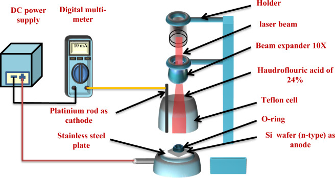
Mirror-like n-type (110) Si wafers with an electrical resistivity of 1–5 mΩ/cm and a thickness of 500 μm, which were purchased from University Wafer, Inc., USA, were utilized. Subsequently, the wafers were sectioned into rectangular pieces, each measuring 1 by 1 cm. Before initiating the photo-electrochemical etching process, the sections underwent a thorough cleaning using an ultrasonic device in ethanol (99.9% concentration, sourced from the German Honeywell company) for a duration of 5 min. The etching process was carried out at room temperature and involved the utilization of a diode laser (660 nm, 100 mW, from the Chinese Tongtool Company), a DC power supply with a voltage range of 0–30 V, and a digital multi-meter (Victor Company). This process, as depicted in Fig. 1, requires the use of a Teflon cell equipped with a cathode electrode made of 95% pure platinum and an anode electrode composed of silicon. The laser played a pivotal role in the top-down electrochemical etching technique employed for the synthesis of the porous silicon (PSi) substrates. Additionally, precise control was maintained over the etching conditions, with a designated etching time of 10 min, a consistently upheld current density of 10 mA/cm2, and a constant concentration of hydrofluoric acid (HF) (sourced from the German company Thomas Baker) at 24%, achieved through the use of the dilution equation51, as depicted in Eq. (1). The concentration of HF used in the etching process was consistently maintained at 24%, and the etching time was precisely set using a digital clock for a duration of 10 min52–56
| 1 |
where C1, hydrofluoric acid concentration; V1, hydrofluoric acid volume; C2, ethanol concentration. V2, ethanol volume.
Figure 1.
A schematic showing how a diode laser can aid the photo-electrochemical etching process52.
Upon completion of the LAECE process, all synthesized P-Si substrates undergo a series of tests to identify the optimal outcome for varying current densities58–60. Structural properties were examined using X-ray diffraction (XRD) equipment (XRD6000 Shimadzu Company) from Japan, utilizing copper radiation with a wavelength of 1.54060 Å. Morphological parameters were evaluated at a high level of detail using German field emission scanning electron microscopy (FESEM) technology (ZEISS Company). Surface characteristics were assessed using atomic force microscopy (AFM) equipment from the TT-2 Workshop Company in the United States. Spectroscopic features were analyzed using photoluminescence (PL) techniques from the Perkin Elmer Company in the United States of America.
Preparation of gallium nitride pellet
A high-purity gallium nitride powder of 99.9%, purchased from Luoyang Advanced Material Company, was compressed into a pellet using a hydraulic compressor with a force of 10 tons. The GaN pellet was subjected to ablation using a Q-switching Nd:YAG laser (RY 280, China) with varying fluences ranging from 530 to 884 mJ/mm2. The laser had a wavelength of 355 nm and a pulse duration of 7 ns, and the ablation process was conducted under a vacuum pressure of 10–2 mbar. The deposition of the GaN film onto the PSi substrate occurred at room temperature. The structure of the GaN film deposited on PSi was examined using an X-ray diffractometer (XRD6000, Shimadzu Company). The morphology of the deposited films was studied using field emission scanning electron microscopy (FESEM) from ZEISS Company. The topography of the deposited films was investigated using an atomic force microscope. Furthermore, the photoluminescence (PL) properties of the films were analyzed using a spectrophotometer from Perkin Elmer.
Electrical properties of GaN/PSi
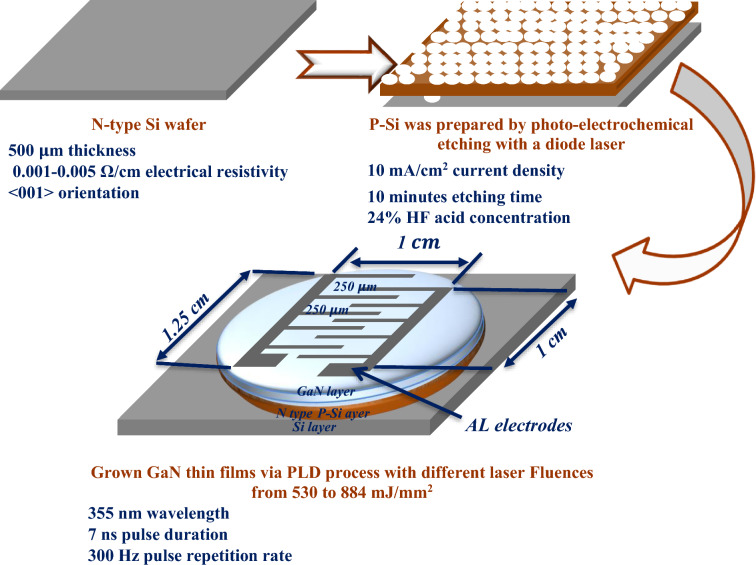
To measure the electrical properties of the GaN/PSi photodetector, a metal interdigitated mask was employed for establishing ohmic contacts. An aluminum film was deposited onto the GaN layer and the backside of the silicon substrate using the thermal evaporation technique, as depicted in Fig. 2. The current–voltage characteristics of the photodetector were measured at room temperature under both dark and illuminated conditions. This was achieved using a power supply (Dazheng 30 V, 5 A PS-305D from China) and digital multi-meters (UNI-T UT33C). Additionally, a programmable LCR meter (LCR-6100, Taiwan, GW Instek, 10 Hz–100 kHz) was employed to evaluate the capacitance–voltage characteristics of the photodetector.
Figure 2.
Process diagram of grown GaN nanostructure.
Figures of merit of the photodetector
The main figures of merit of the photodetector, namely responsivity (R), specific detectivity (D*), and external quantum efficiency (EQE) were measured using photodetector evaluation system. It is consists of monochromator (Jobin-Yuvon), beam spilter, halogen lamp, multimeter, and silicon power meter. These measurements were conducted out under a reverse bias of 3 V.
Results and discussion
XRD properties
Figure 3 depicts the XRD pattern of the PSi, revealing two peaks situated at 2θ = 33° and 68°, which correspond to the (200) and (400) planes, respectively. These two peaks are characteristic of porous silicon and align well with findings reported previously61–66. The XRD analysis of PSi confirms the splitting of the peak at 68° into two distinct peaks, representing crystalline silicon and porous silicon..
Figure 3.
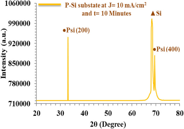
XRD pattern of PSi substrate.
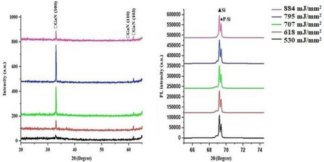
Figure 4 depicts the XRD pattern of GaN nanocrystalline films deposited on PSi at various laser fluences. Three peaks were observed for all GaN films; these peaks are located at 2θ = 32.8°, 57.9°, and 61.7°, corresponding to (100), (110), and (103) planes, respectively. These peaks are indexed to GaN according to JCPDS # 01-074-0243. With an increase in laser fluence, a slight shift in 2θ was detected, and there was an observed increase in peak intensity along the (100) plane. The slight shift is attributed to stress and strain, while the increase in peak intensity is attributed to the greater film thickness and grain size.
Figure 4.
XRD pattern of GaN nano-crystalline films on a P-Si substrate using laser fluences ranging from 530 to 884 J.
The XRD analysis of the PSi substrate and the GaN films deposited on PSi is presented in Tables 1 and 2, respectively. To determine the crystallite size (D), Scherrer’s formula67–70 was employed, while the interplanar distance (d) was calculated using the formula71–74
| 2 |
| 3 |
where K is a constant set at 0.9, λ is the wavelength of the CuKα source, β is the fullwidth at half maximum of the XRD pattern, is the diffraction angle, and n is a positive integer.
Table 1.
X-Ray diffraction pattern of fabricated P-Si layer.
| Substrate orientation (hkl) |
2 theta (Degree) |
Full width at half maximum (Degree) |
Crystallite size (nm) |
Interplanner spacing (nm) |
|---|---|---|---|---|
| <200> | 33.101 | 0.290 | 0.282 | 0.211 |
| <400> | 69.331 | 0.321 | 0.141 | 0.142 |
Table 2.
XRD pattern of GaN nano-crystalline films over P-Si substrate.
| Laser Fluence (mJ/mm2) |
Film orientation (hkl) |
2theta (Degree) |
Full width at half maximum (Degree) |
Crystallite size (nm) |
Interplanner spacing (nm) |
|---|---|---|---|---|---|
| 530 | <100> | 32.840 | 0.390 | 21.260 | 0.271 |
| <110> | 57.921 | 0.170 | 53.471 | 0.152 | |
| <103> | 61.720 | 0.170 | 54.501 | 0.151 | |
| 618 | <100> | 33.0 | 0.202 | 40.861 | 0.271 |
| <110> | 58.921 | 0.150 | 60.900 | 0.152 | |
| <103> | 61.761 | 0.141 | 66.202 | 0.151 | |
| 707 | <100> | 33.041 | 0.181 | 46.090 | 0.271 |
| <110> | 59.160 | 0.230 | 39.762 | 0.152 | |
| <103> | 61.761 | 0.161 | 57.922 | 0.151 | |
| 795 | <100> | 33.041 | 0.170 | 48.801 | 0.271 |
| <110> | 59.801 | 0.061 | 152.932 | 0.152 | |
| <103> | 61.760 | 0.130 | 71.291 | 0.151 | |
| 884 | <100> | 33.041 | 0.171 | 48.802 | 0.271 |
| <110> | 59.761 | 0.050 | 183.481 | 0.152 | |
| <103> | 61.760 | 0.131 | 71.292 | 0.151 |
Spectroscopic properties
The photoluminescence (PL) spectra of the PSi substrate are depicted in Fig. 5. PL measurements of the PSi substrate were conducted at room temperature with an excitation wavelength of 280 nm. Firstly, it is observed that the prepared PSi substrate exhibits an emission peak at 589 nm, which belongs to the visible yellow band. This peak is attributed to surface states and quantum confinement arising during the photo-electrochemical etching process, as mentioned by Wang75–78. The energy band gap of the prepared PSi substrate was determined to be 2.1 eV, larger than the energy band gap of crystalline silicon (1.11 eV). This difference in energy band gaps can be attributed to the combined effects of quantum confinement and increased surface states, altering the electronic structure of the material.
Figure 5.
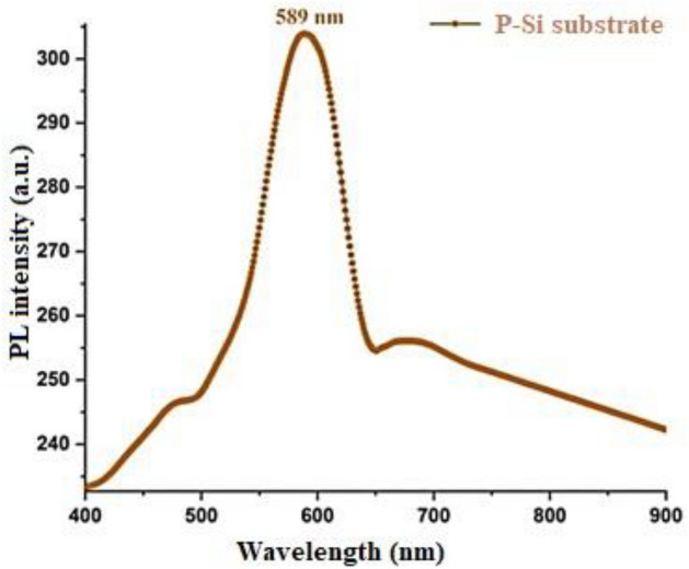
Room temperature photoluminescence prepared P-Si substrate.
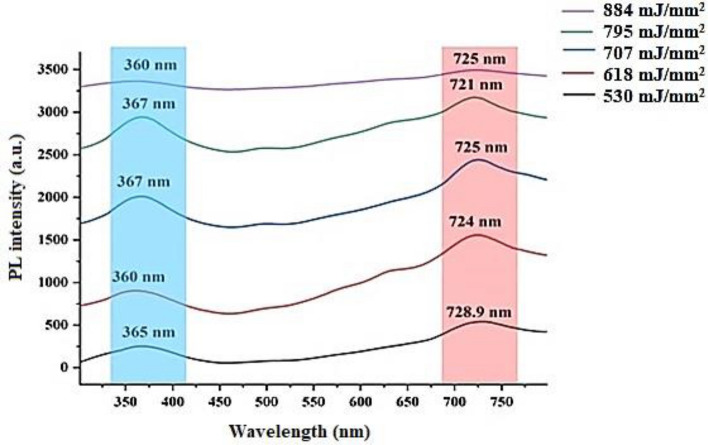
The PL spectra of GaN nanocrystalline films prepared at different laser fluences are depicted in Fig. 6. The PL of GaN/P-Si nanocrystalline films was measured at room temperature, and the excitation wavelength was 320 nm. The PL spectra of the GaN nanocrystalline films exhibited UV bands located at 265.9, 267.9, 267, 260, and 260.9 nm, which are attributed to the GaN film, as well as red bands at 628.9, 621, 625.9, 624, and 625 nm, which belong to the P-Si substrate. Increasing the laser fluence led to a decrease in the PL intensity, but there were differing opinions regarding the peak location of the PL spectrum. This discrepancy was likely due to the higher defect density causing more non-radiative recombination. According to the PL results, the energy gaps for GaN nanofilms prepared at laser fluences of 530, 618, 707, 884, and 795 mJ/mm2 are 3.45, 3.38, 3.36, 3.34, and 3.44 eV, respectively, which are in agreement with the reported data58,79–81.
Figure 6.
Room temperature PL spectra of GaN/PSi nanostructures prepared at various laser fluences.
Surface topography AFM
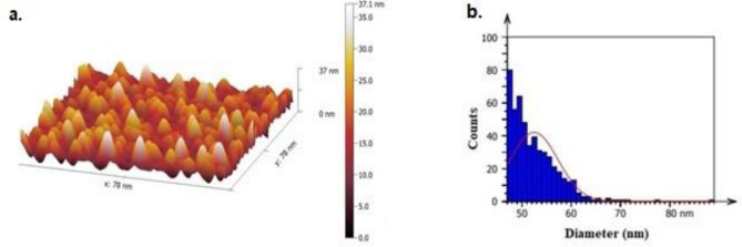
Figure 7 a,b depicts the 3D AFM images and the grain size distribution of P-Si substrate etched. In contrast, after 10 min of etching, the pores formed uniformly throughout the entire surface, taking on a more elongated oval shape. Table 3 provides the AFM parameters of a prepared P-Si substrate. Most notably, nanometer-scale research into particle size distribution was conducted on the P-Si substrate after preparation.
Figure 7.
(a) AFM image of prepared P-Si substrate; (b) grain size distribution of prepared P-Si substrate.
Table 3.
AFM parameters of PSi substrate.
| Root-mean-square height (nm) | Maximum height (nm) |
Average surface roughness (nm) |
Average diameter (nm) |
|---|---|---|---|
| 11.880 | 88.660 | 9.400 | 52.460 |
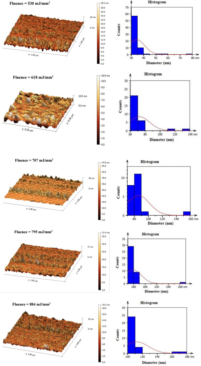
To analyze and characterize the topography of the prepared GaN nano-crystalline films over a PSi substrate, Fig. 8 depicts three-dimensional AFM images and grain size distribution. Average particle diameter and average surface roughness increased as laser Fluence increased from 530 to 884 mJ/mm2, but they decreased at 884 mJ/mm2, as demonstrated in Table 4. The AFM image of the GaN nanocrystalline film shows the uniform deposition of samples created with 795 mJ/mm2 laser Fluence and the largest average particle diameter and average surface roughness.
Figure 8.
AFM and grain size distribution images of GaN/PSi nanostructures prepared at various laser fluences.
Table 4.
AFM parameters of GaN/PSi nanostructures prepared at various laser fluences.
| Laser fluence (mJ/mm2) | Root-mean-square height (nm) | Maximum height (nm) |
Average surface roughness (nm) | Average diameter (nm) |
|---|---|---|---|---|
| 530 | 15.962 | 78.011 | 13.832 | 34.411 |
| 618 | 34.411 | 131.701 | 28.423 | 72.051 |
| 707 | 46.822 | 154.321 | 42.521 | 85.932 |
| 795 | 59.012 | 265.301 | 50.610 | 178.83 |
| 884 | 33.853 | 179.702 | 26.012 | 112.222 |
Surface morphology FESEM
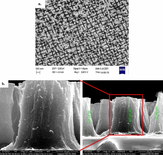
Figure 9a and b depicts FE-SEM images of the surface and cross-section, respectively, of the PSi substrates, offering insights into the surface morphology. According to the research conducted by Omar et al.67, the pores on the surface exhibit a star-like appearance and maintain an elongated shape across the entire surface. This is attributed to the use of n-type silicon (100) with low resistivity during the preparation of the PSi82–85. Furthermore, the FE-SEM cross-sectional image revealed that the thickness of the P-Si layer measures 36.02 μm.
Figure 9.
FE-SEM images of prepared P-Si substrate, a. surface area image, and b. cross section image.
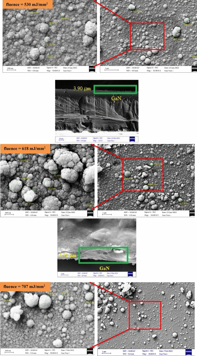
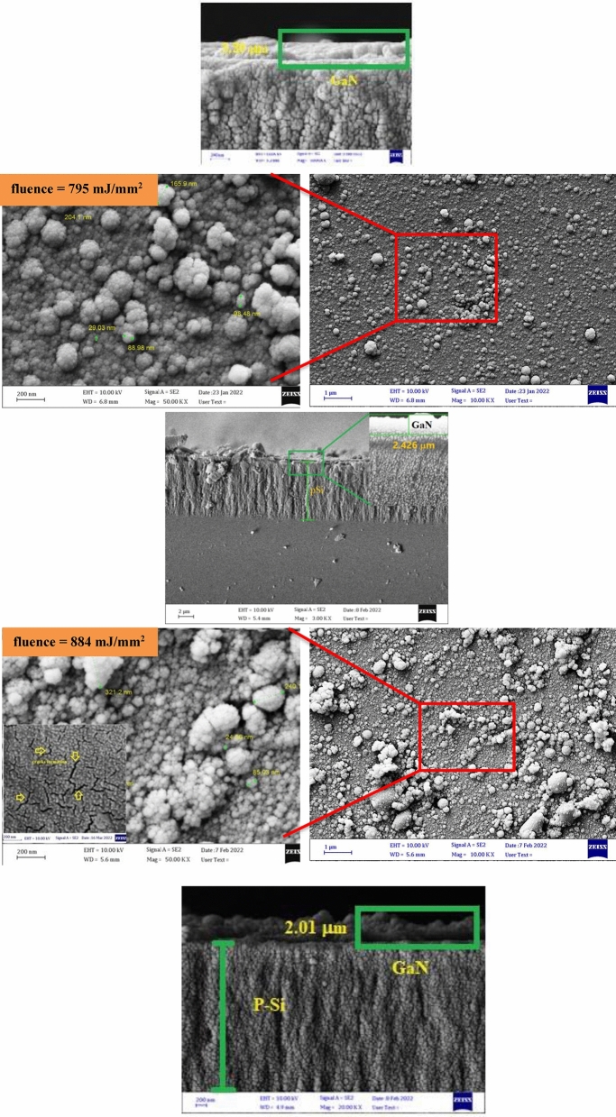
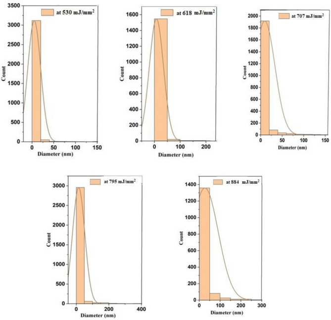
Figure 10 depicts FE-SEM images of GaN/PSi nanostructures produced using PLD at varying laser intensities. This study revealed that the thickness of the GaN nanocrystalline film produced with a laser fluence of 795 mJ/mm2 during the PLD process measures approximately 383.36 nm, which is comparable to the thickness of the GaN nanostructures themselves. The surface morphology of the GaN films was analyzed using micro- and nano-scale techniques. As depicted in Fig. 11, the average diameter of GaN/PSi nanostructures created with different laser fluences was calculated through ImageJ analysis. Furthermore, the GaN nano-crystalline films fully covered the P-Si substrate, resulting in uniform and homogeneously-sized spherical particles with a cauliflower-like shape.
Figure 10.
FE-SEM images and cross section images of GaN/PSi nanostructures prepared at various laser fluences.
Figure 11.
Average diameter images of GaN/PSi nanostructures prepared at various laser fluences.
Electrical properties
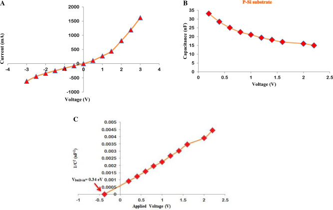
At room temperature, the dark current–voltage characteristic of the prepared P-Si substrate was analyzed in the dark, as depicted in Fig. 12A. As the voltage was applied, the current flowing through the P-Si substrate increased due to the elevated resistance of the P-Si layer with increasing voltage86,87. Moreover, the charge transfer led to the formation of a depletion zone in the prepared P-Si substrate close to the electrical dipole, resulting in a rectifying characteristic88–90.
Figure 12.
Electrical characteristic of prepared P-Si substrate, (A) dark I–V characteristic for forward and reverse bias, (B) C–V characteristic, (C) 1/C2 vs. voltage.
Figure 12B depicts the capacitance–voltage characteristic for applied voltages ranging from 0 to 3 V. The capacitance of the prepared P-Si substrate decreased. This phenomenon has been coined as the “growing depletion region with increasing built-in potential”57,91–94.was coined to describe this phenomenon.
The relationship between 1/C2 and the voltage on the fabricated P-Si substrate is depicted in Fig. 12C. C2 exhibits a linear relationship with voltage. Figure 12C shows the correlation between 1/C2 and voltage on a prepared PSi substrate. a linear relationship with voltage. The built-in potential was determined by extending the given linear segment of the curve to a 1/C2 value of 0 points. There was an inherent potential of 0.34 eV.
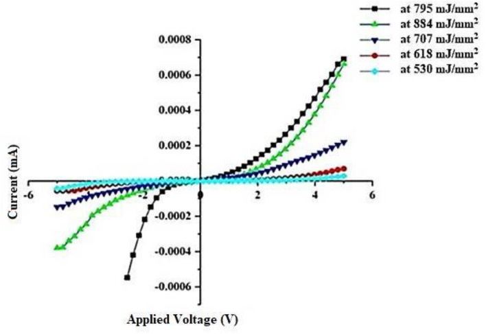
Figure 13 depicts the dark I–V characteristics of GaN nanocrystalline films fabricated on a P-Si substrate using the PLD method at various laser fluences and at room temperature. As the bias voltage was increased, the GaN nano-crystalline film created at 795 mJ/mm2 exhibited expansion due to the narrowing of the depletion layer95,96.
Figure 13.
PLD-fabricated GaN/PSi nanostructure dark I–V properties at laser fluences between 530 and 884 mJ/mm2 under forward and reverse biases.
Furthermore, rectification features were observed in the GaN/P-Si nanocrystalline film, and recombination tunneling served as the current transport mechanism in both layers97–99.
Performance characterization of GaN nanostructure with optimum laser fluence
The performance properties of the fabricated GaN/PSi heterojunction using the PLD method with optimal laser parameters (355 nm laser wavelength and 300 °C substrate temperature) at different laser fluences were determined, and they are illustrated in Figs. 15, 16, 17 and 18. The study concluded that a laser Fluence value of 795 mJ/mm2 was optimal. The responsivity (Rλ), specific detectivity (Dλ), and external quantum efficiency (EQE) of the produced GaN nano-crystalline film were assessed. Responsivity (Rλ) can be calculated using Eq. (4)57,96,100,101, which stands as a significant figure of merit. Both Eqs. (5) and (6)102–105 represent detectivity (D*) and external quantum efficiency (EQE), respectively
| 4 |
Iph is the photocurrent (Ampere), and P is the incident power (Watt)106,107.
| 5 |
where A is the area of photodetector, is the dark current of photodetector, and q is the electron charge108–111.
| 6 |
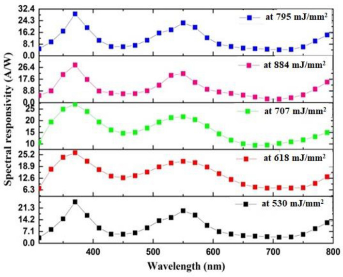
Figure 14 depicts the responsivity of the structure when subjected to varying laser intensities operating between 350 and 850 nm. Three response peaks of 29.010 A/W at 370 nm and 22.761 A/W at 550 nm were observed in the fabricated GaN on P-Si nanostructure at 795 mJ/mm2, which can be attributed to the larger surface area, extended depletion layer width, and increased minority carrier diffusion length112.
Figure 14.
Spectral responsivityof fabricated GaN/P-Si nanostructure at 355 nm, 300 °C and different laser fluences.
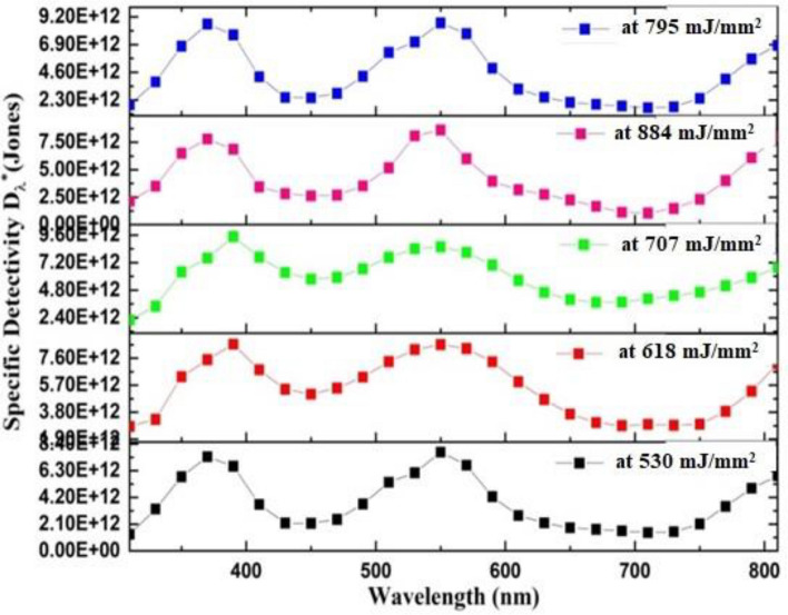
Figure 15 depicts variation of detectivity (D*) with wavelength of the GaN/P-Si photodetectors. Two peaks were observed at 355 nm and 550 nm.
Figure 15.
Detectivity of GaN/P-Si heterojunction photodetectors fabricated at different laser fluences under − 3 V bias.
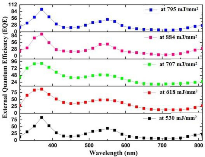
Figure 16 depicts the EQE of GaN/PSi photodetectors fabricated at various laser fluences. Among these, the photodetector fabricated at 795 mJ/mm2 achieved the highest EQE values: 93.240% at 370 nm and 51.30% at 550 nm. The GaN/PSi heterojunction photodetector fabricated at 795 mJ/mm2 demonstrated a high EQE due to the direct relationship with Eq. (6), driven by its strong spectral response. Enhancing the reverse bias voltage can improve the collection efficiency of photogenerated carriers, allowing for the creation of a fully depleted photodetector113,114.
Figure 16.
External quantum efficiency of GaN/P-Si nanostructure fabricated at different laser fluences.
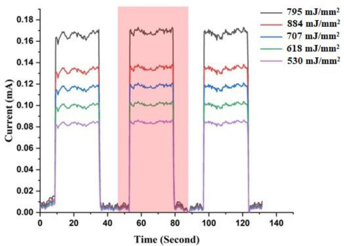
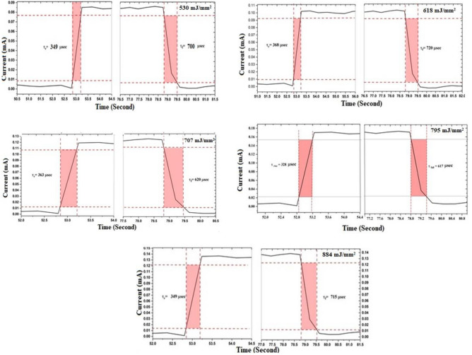
Figures 17 and 18 depict the dynamic photoresponse switching of the photodetectors deposited at various laser fluences. Three distinct switching cycles were conducted, each with an 18-s off period followed by a 25-s on period. Rise and fall times of the fabricated GaN/P-Si nanostructure were measured from 10 to 90% of the peak signal and from 90 to 10% of the peak signal, respectively. The photodetector prepared with a laser fluence of 795 mJ/mm2 exhibits a switching characteristic, with a measured rise time of 363 μs and a fall time of 711 μs.
Figure 17.
A switching characteristic of GaN/P-Si nanostructure fabricated at different laser fluences.
Figure 18.
Rise time and fall time of GaN/PSi heterojunction photodiode fabricated at different laser fluences.
The fabricated GaN/P-Si nanocrystalline film at 795 mJ/mm2 exhibited the best performance, with a responsivity of 29.010 A/W at 370 nm, a detectivity of 8.61 × 10¹² Jones, and an external quantum efficiency of 93.240%. Additionally, it demonstrated a fast response rise time of 328 and a fall time of 617, outperforming Jiang et al. (2022), who fabricated a GaN/Si UV photodetector using a chemical vapor deposition process. Their device showed a responsivity of 71.4 mA/W, detectivity of 7.1 × 10⁸ Jones, external quantum efficiency of 24.3%, and a response time of 0.2/7.6 s115. Table 5 provides a summary of the figures of merit for the GaN/PSi photodetectors fabricated at various laser fluences.
Table 5.
Shows the results of testing a manufactured GaN/P-Si nanostructure fabricated at different laser fluences.
| Laser fluence (mJ/mm2) |
Spectral responsivity (A/W) |
Specific detectivity (Jones) |
External quantum efficiency (%) |
Rise time () |
Fall time () |
|---|---|---|---|---|---|
| 530 | 25.011 at 370 nm | 7.40 × 10+12 | 83.801 | 349 | 700 |
| 19.620 at 550 nm | 7.750 × 10+12 | 44.212 | |||
| 618 | 26.271 at 370 nm | 7.51 × 10+12 | 88.051 | 368 | 720 |
| 21.660 at 575 nm | 8.51 × 10+12 | 48.812 | |||
| 707 | 27.081 at 370 nm | 7.60 × 10+12 | 89.512 | 363 | 620 |
| 21.701 at 555 nm | 8.50 × 10+12 | 48.911 | |||
| 795 | 29.010 at 370 nm | 8.61 × 10+12 | 93.240 | 328 | 617 |
| 22.762 at 555 nm | 8.70 × 10+12 | 51.306 | |||
| 884 | 28.192 at 370 nm | 7.81 × 10+12 | 90.702 | 349 | 715 |
| 21.811 at 555 nm | 8.60 × 10+12 | 49.110 |
Conclusion
Nanostructured GaN/PSi photodetectors were successfully fabricated using the pulsed laser deposition method at various laser fluences. The GaN nanostructure film deposited at 795 mJ/mm2 exhibited high crystalline peaks with a large crystallite size, indicating favorable structural characteristics. Spectroscopically, this film exhibited a shorter wavelength of 260 nm and a high energy gap of 4.76 eV. Morphologically, the film showed uniform, homogeneous spherical particles resembling cauliflower, with a thickness of 383.36 nm. Additionally, a uniform deposition yielded the largest average particle diameter (178.8 nm) and average surface roughness (50.61 nm).
Furthermore, performance characteristics were assessed for GaN nanostructures prepared using a laser fluence of 795 mJ/mm2. Due to the energy gap of GaN material, the responsivity under 3 V exhibited maximum values: responsivity of approximately 29.03 A/W, detectivity of 8.6 × 10¹² Jones, and an external quantum efficiency of 97.2% at 370 nm. Similarly, at 575 nm, the responsivity measured around 19.86 A/W, detectivity of 8.9 × 10¹² Jones, and an external quantum efficiency of 50.89%.
Additionally, three switching cycles with an 18-s off period and a 25-s on period were illuminated with a power of 100 mW/cm2. The rise time of the fabricated GaN/P-Si nanostructure was 328 μs, while the fall time was 617 μs. A strong correlation was observed between the optimum laser Fluence (795 mJ/mm2) and the achieved GaN nanostructure performance characteristics.
Acknowledgements
The authors would like to thank the University of Technology-Iraq for the logistic support this work. The authors extend their appreciation to the Deanship of Scientific Research at Northern Border University, Arar, KSA for support this research work through the project number “NBU-FFR-2023-0139. The authors gratefully thank the Prince Faisal bin Khalid bin Sultan Research Chair in Renewable Energy Studies and Applications (PFCRE) at Northern Border University for their support and assistance. The authors would like to thank Al-Farahidi University, Baghdad, Iraq for the logistic support this work.
Author contributions
M.A.F., H.D.J., M.J.A., E.T.S., A.S.A., R.K.I., R.A.I., conceptualization, M.A.F., H.D.J., M.J.A., E.T.S; methodology, M.A.F., H.D.J., M.J.A., E.T.S; validation, M.A F., E.T.S., A.S.A., R.K.I., R.A.I.; formal analysis, M.A.F., H.D.J., M.J.A., E.T.S.; investigation, M.A.F., H.D.J., E.T.S., A.S.A., R.K.I., R.A.I.; resources, M.A.F., E.T.S., A.S.A., R.K.I., R.A.I.; data curation, M.A.F., H.D.J., E.T.S.; writing—original draft preparation, H.D.J.; writing—review and editing, M.A.F., M.J.A., E.T.S., A.S.A., R.K.I., R.A.I.; visualization, M.A.F., H.D.J., M.J.A., E.T.S., A.S.A., R.K.I., R.A.I.; supervision, M.A.F., M.J.A.; project administration, M.A.F., M.J.A., E.T.S.; funding acquisition, A.S.A., all authors have read and agreed to the published version of the manuscript.
Data availability
Correspondence and requests for materials should be addressed to Makram A. Fakhri, Haneen D. Jabbar, and Evan T. Salim.
Competing interests
The authors declare no competing interests.
Footnotes
Publisher's note
Springer Nature remains neutral with regard to jurisdictional claims in published maps and institutional affiliations.
Contributor Information
Makram A. Fakhri, Email: mokaram_76@yahoo.com, Email: makram.a.fakhri@uotechnology.edu.iq
Evan T. Salim, Email: evan_tarq@yahoo.com, Email: evan.t.salim@uotechnology.edu.iq
Ahmad S. Azzahrani, Email: ahmad.azzahrani@nbu.edu.sa
References
- 1.Chen F, Ji X, Lau SP. Recent progress in group III-nitride nanostructures: From materials to applications. Mater. Sci. Eng. R. Rep. 2020;142:100578. doi: 10.1016/j.mser.2020.100578. [DOI] [Google Scholar]
- 2.Feng ZC, editor. III-Nitride Materials. World Scientific; 2017. [Google Scholar]
- 3.Gil B. III-Nitride Semiconductors and Their Modern Devices. OUP Oxford; 2013. [Google Scholar]
- 4.Kneissl M, Rass J. III-Nitride Ultraviolet Emitters. Springer; 2016. [Google Scholar]
- 5.Ben J, Liu X, Wang C, Zhang Y, Shi Z, Jia Y, Sun X, et al. 2D III-Nitride materials: Properties, growth, and applications. Adv. Mater. 2021;33(27):2006761. doi: 10.1002/adma.202006761. [DOI] [PubMed] [Google Scholar]
- 6.Flack TJ, Pushpakaran BN, Bayne SB. GaN technology for power electronic applications: A review. J. Electron. Mater. 2016;45(6):2673–2682. doi: 10.1007/s11664-016-4435-3. [DOI] [Google Scholar]
- 7.Boles, T. (GaN-on-silicon present challenges and future opportunities. In 2017 12th European Microwave Integrated Circuits Conference (EuMIC) 21–24 (IEEE, 2017).
- 8.Amir HAAA, Fakhri MA, Alwahib AA, Salim ET, Alsultany FH, Hashim U. Synthesis of gallium nitride nanostructure using pulsed laser ablation in liquid for photoelectric detector. Mater. Sci. Semicond. Process. 2022;150:106911. doi: 10.1016/j.mssp.2022.106911. [DOI] [Google Scholar]
- 9.Abud SH, Selman AM, Hassan Z. Investigation of structural and optical properties of GaN on flat and porous silicon. Superlattices Microstruct. 2016;97:586–590. doi: 10.1016/j.spmi.2016.07.017. [DOI] [Google Scholar]
- 10.Jabbar HD, Fakhri MA, AbdulRazzaq MJ. Gallium nitride-based photodiode: A review. Mater. Today: Proc. 2021;42:2829–2834. [Google Scholar]
- 11.Roccaforte F, Fiorenza P, Lo Nigro R, Giannazzo F, Greco G. Physics and technology of gallium nitride materials for power electronics. La Riv. Nuovo Cimen. 2018;41(12):625–681. [Google Scholar]
- 12.Al-Zuhairi O, Shuhaimi A, Nayan N, Azman A, Kamarudzaman A, Alobaidi O, Zhu Y, et al. Non-polar gallium nitride for photodetection applications: A systematic review. Coatings. 2022;12(2):275. doi: 10.3390/coatings12020275. [DOI] [Google Scholar]
- 13.Amir HAAA, Fakhri MA, Alwahib AA, Salim ET. Synthesize of GaN/quartz nanostructure using pulsed laser ablation in liquid for optoelectronic devices. Sens. Actuat. B: Chem. 2021;2021:2163. [Google Scholar]
- 14.Amir HAAA, Fakhri MA, Alwahib AA, Salim ET, Alsultany FH, Hashim U. An investigation on GaN/Porous-Si NO2 gas sensor fabricated by pulsed laser ablation in liquid. Sens. Actuat. B: Chem. 2022;2022:132163. doi: 10.1016/j.snb.2022.132163. [DOI] [Google Scholar]
- 15.Aggarwal N, Gupta G. Enlightening gallium nitride-based UV photodetectors. J. Mater. Chem. C. 2020;8(36):12348–12354. doi: 10.1039/D0TC03219K. [DOI] [Google Scholar]
- 16.Xu W, Shi Y, Ren F, Zhou D, Su L, Liu Q, Lu H, et al. Magnesium ion-implantation-based gallium nitride pin photodiode for visible-blind ultraviolet detection. Photon. Res. 2019;7(8):B48–B54. doi: 10.1364/PRJ.7.000B48. [DOI] [Google Scholar]
- 17.Pham TTT, Shin H, Chong E, Cha HY. Gallium nitride PIN avalanche photodiode with double-step mesa structure. J. Semicond. Technol. Sci. 2018;18(5):645–649. doi: 10.5573/JSTS.2018.18.5.645. [DOI] [Google Scholar]
- 18.Yakuphanoglu F, Shokr FS, Gupta RK, Al-Ghamdi AA, Bin-Omran S, Al-Turki Y, El-Tantawy F. A new type photodiode: p-Si/GaN pn junction in series with GaN/Ag Schottky diode. J. Alloy. Compd. 2015;650:671–675. doi: 10.1016/j.jallcom.2015.08.025. [DOI] [Google Scholar]
- 19.Ji MH, Kim J, Detchprohm T, Dupuis RD, Sood AK, Dhar NK, Lewis J. Uniform and reliable GaN pin ultraviolet avalanche photodiode arrays. IEEE Photon. Technol. Lett. 2016;28(19):2015–2018. doi: 10.1109/LPT.2016.2580038. [DOI] [Google Scholar]
- 20.Bakhtiary-Noodeh, M. et al. Demonstration of uniform 6x6 GaN pin UV avalanche photodiode arrays. In Gallium Nitride Materials and Devices XVI, vol. 11686 93–100 (SPIE, 2021).
- 21.Griffiths AD, Herrnsdorf J, McKendry JJD, Strain MJ, Dawson MD. Gallium nitride micro-light-emitting diode structured light sources for multi-modal optical wireless communications systems. Philos. Trans. R. Soc. A. 2020;378(2169):20190185. doi: 10.1098/rsta.2019.0185. [DOI] [PMC free article] [PubMed] [Google Scholar]
- 22.Wang Y, Fan S, Alotaibi B, Wang Y, Li L, Mi Z. A monolithically integrated gallium nitride nanowire/silicon solar cell photocathode for selective carbon dioxide reduction to methane. Chem. Eur. J. 2016;22(26):8809–8813. doi: 10.1002/chem.201601642. [DOI] [PubMed] [Google Scholar]
- 23.Zulkifli NAA, Park K, Min JW, Ooi BS, Zakaria R, Kim J, Tan CL. A highly sensitive, large area, and self-powered UV photodetector based on coalesced gallium nitride nanorods/graphene/silicon (111) heterostructure. Appl. Phys. Lett. 2020;117(19):191103. doi: 10.1063/5.0018076. [DOI] [Google Scholar]
- 24.Li G, Wang W, Yang W, Wang H. Epitaxial growth of group III-nitride films by pulsed laser deposition and their use in the development of LED devices. Surf. Sci. Rep. 2015;70(3):380–423. doi: 10.1016/j.surfrep.2015.06.001. [DOI] [Google Scholar]
- 25.Wong S, Jaluria Y. A numerical and experimental study on the fabrication GaN films by chemical vapor deposition. J. Manuf. Sci. Eng. 2020;142(1):011001. doi: 10.1115/1.4044712. [DOI] [Google Scholar]
- 26.Wang W, Wang H, Yang W, Zhu Y, Li G. A new approach to epitaxially grow high-quality GaN films on Si substrates: The combination of MBE and PLD. Sci. Rep. 2016;6(1):1–11. doi: 10.1038/srep24448. [DOI] [PMC free article] [PubMed] [Google Scholar]
- 27.Shetty, A. et al. (Plasmonic enhancement of photocurrent in GaN based UV photodetectors. In 2014 IEEE 2nd International Conference on Emerging Electronics (ICEE) 1–4 (IEEE, 2014).
- 28.Salim ET, Hassan AI, Naaes SA. Effect of gate dielectric thicknesses on MOS photodiode performance and electrical properties. Mater. Res. Express. 2019;6(8):086416. doi: 10.1088/2053-1591/ab1bc2. [DOI] [Google Scholar]
- 29.Lin JC, Su YK, Chang SJ, Lan WH, Huang KC, Chen WR, Cheng YC, et al. High responsivity of GaN p-i-n photodiode by using low-temperature interlayer. Appl. Phys. Lett. 2007;91(17):173502. doi: 10.1063/1.2800813. [DOI] [Google Scholar]
- 30.ElFaham MM, Mostafa AM, Toghan A. Facile synthesis of Cu2O nanoparticles using pulsed laser ablation method for optoelectronic applications. Colloids Surf. A. 2021;630:127562. doi: 10.1016/j.colsurfa.2021.127562. [DOI] [Google Scholar]
- 31.Tareq HS. Deposited nanostructure cds thin film by using pulse laser deposition technique for fabrication of heterojunction solar cell. Eng. Tech. J. 2014;32:141. [Google Scholar]
- 32.Abdulkareem KA, Kadhim SM, Ali SB. The structural and optical properties of nanocrystalline Fe3O4 thin films prepared by PLD. Eng. Technol. J. 2022;40(02):334–342. doi: 10.30684/etj.v40i2.2235. [DOI] [Google Scholar]
- 33.Abdul Amir HAA, Fakhri MA, Alwahib A. Synthesized of GaN nanostructure using 1064 nm laser wavelength by pulsed laser ablation in liquid. Eng. Technol. J. 2022;40(2):404–411. doi: 10.30684/etj.v40i2.2271. [DOI] [Google Scholar]
- 34.Taleb, S. M., Fakhri, M. A., & Adnan, S. A. Optical investigations of nanophotonic LiNbO3 films deposited by pulsed laser deposition method. In Defect and Diffusion Forum, vol. 398 16–22 (Trans Tech Publications Ltd, 2020).
- 35.Khalid, F. G., Ibraheam, A. S., Fakhri, M. A., & Numan, N. H. Some of the electrical and thermoelectrical properties for Cdo thin films preperaerd using pulsed laser deposition method. In AIP Conference Proceedings, vol. 2213 020204 (AIP Publishing LLC, 2020).
- 36.Fakhri MA, et al. Synthesis of LiNbO3/SiO2/Si nanostructures layer by layer based on mach-zehnder modulator using pulsed laser deposition route. Silicon. 2022;2022:1–15. [Google Scholar]
- 37.Chidambaram PR, Bowen C, Chakravarthi S, Machala C, Wise R. Fundamentals of silicon material properties for successful exploitation of strain engineering in modern CMOS manufacturing. IEEE Trans. Electron. Dev. 2006;53(5):944–964. doi: 10.1109/TED.2006.872912. [DOI] [Google Scholar]
- 38.Basu, S. (Ed.). Crystalline Silicon: Properties and Uses. (BoD–Books on Demand, 2011).
- 39.Sun, P., Xu, P., Zhu, K., & Zhou, Z. Silicon-based optoelectronics enhanced by hybrid plasmon polaritons: Bridging dielectric photonics and nanoplasmonics. In Photonics, vol. 8 482. MDPI (2021).
- 40.Sharma P, Sun X, Parish G, Keating A. Optimising porous silicon electrical properties for thermal sensing applications. Micropor. Mesopor. Mater. 2021;312:110767. doi: 10.1016/j.micromeso.2020.110767. [DOI] [Google Scholar]
- 41.Vercauteren R, Scheen G, Raskin JP, Francis LA. Porous silicon membranes and their applications: Recent advances. Sens. Actuat. A. 2021;318:112486. doi: 10.1016/j.sna.2020.112486. [DOI] [Google Scholar]
- 42.Jung Y, Huh Y, Kim D. Recent advances in surface engineering of porous silicon nanomaterials for biomedical applications. Micropor. Mesopor. Mater. 2021;310:110673. doi: 10.1016/j.micromeso.2020.110673. [DOI] [Google Scholar]
- 43.Moretta R, De Stefano L, Terracciano M, Rea I. Porous silicon optical devices: Recent advances in biosensing applications. Sensors. 2021;21(4):1336. doi: 10.3390/s21041336. [DOI] [PMC free article] [PubMed] [Google Scholar]
- 44.Jenie SN, Plush SE, Voelcker NH. Recent advances on luminescent enhancement-based porous silicon biosensors. Pharmaceut. Res. 2016;33(10):2314–2336. doi: 10.1007/s11095-016-1889-1. [DOI] [PubMed] [Google Scholar]
- 45.Congli S, Hao H, Huanhuan F, Jingjing X, Yu C, Yong J, Xiaosong S, et al. Synthesis of porous silicon nano-wires and the emission of red luminescence. Appl. Surface Sci. 2013;282:259–263. doi: 10.1016/j.apsusc.2013.05.114. [DOI] [Google Scholar]
- 46.Arshavsky-Graham S, Massad-Ivanir N, Segal E, Weiss S. Porous silicon-based photonic biosensors: Current status and emerging applications. Anal. Chem. 2018;91(1):441–467. doi: 10.1021/acs.analchem.8b05028. [DOI] [PubMed] [Google Scholar]
- 47.Canham L, editor. Handbook of Porous Silicon. Springer International Publishing; 2014. pp. 163–170. [Google Scholar]
- 48.Kim DH, Lee W, Myoung JM. Flexible multi-wavelength photodetector based on porous silicon nanowires. Nanoscale. 2018;10(37):17705–17711. doi: 10.1039/C8NR05096A. [DOI] [PubMed] [Google Scholar]
- 49.Ismail RA, Alwan AM, Ahmed AS. Preparation and characteristics study of nano-porous silicon UV photodetector. Appl. Nanosci. 2017;7(1):9–15. doi: 10.1007/s13204-016-0544-9. [DOI] [Google Scholar]
- 50.Santos HA, Mäkilä E, Airaksinen AJ, Bimbo LM, Hirvonen J. Porous silicon nanoparticles for nanomedicine: Preparation and biomedical applications. Nanomedicine. 2014;9(4):535–554. doi: 10.2217/nnm.13.223. [DOI] [PubMed] [Google Scholar]
- 51.Jabbar HD, Fakhri MA, Razzaq MJA, Dahham OS, Salim ET, Alsultany FH, Hashim U. Effect of different etching time on fabrication of an optoelectronic device based on GaN/Psi. J. Renew. Mater. 2023;11(3):1101–1122. doi: 10.32604/jrm.2023.023698. [DOI] [Google Scholar]
- 52.Jabbar HD, Fakhri MA, AbdulRazzaq MJ. Synthesis gallium nitride on porous silicon nano-structure for optoelectronics devices. Silicon. 2022;2022:1–17. [Google Scholar]
- 53.Hattab, F. & Fakhry, M. Optical and structure properties for nano titanium oxide thin film prepared by PLD. In 2012 First National Conference for Engineering Sciences (FNCES 2012). 10.1109/NCES.2012.6740474.
- 54.Asady H, Salim ET, Ismail RA. Some critical issues on the structural properties of Nb2O5 nanostructure film deposited by hydrothermal technique. AIP Conf. Proc. 2020;2213(1):020183. doi: 10.1063/5.0000214. [DOI] [Google Scholar]
- 55.Fakhri MA, Al-Douri Y, Hashim U. Fabricated optical strip waveguide of nanophotonics lithium niobate. IEEE Photon. J. 2016;8(2):4500410. doi: 10.1109/JPHOT.2016.2531583. [DOI] [Google Scholar]
- 56.Mohammed FA, Salim ET, Hassan AI, Wahid MHA. Effect of precursor concentration on the structural, optical, and electrical properties of WO3 thin films prepared by spray pyrolysis. J. Appl. Sci. Nanotechnol. 2022;2(4):91–105. doi: 10.53293/jasn.2022.4715.1139. [DOI] [Google Scholar]
- 57.Fakhri MA, Numan NH, Mohammed QQ, Abdulla MS, Hassan OS, Abduljabar SA, Ahmed AA. Responsivity and response time of nano silver oxide on silicon heterojunction detector. Int. J. Nanoelectron. Mater. 2018;11(21):65–72. [Google Scholar]
- 58.Alwazny MS, Ismail RA, Salim ET. Optical properties of lithium niobate nanoparticles prepared by laser ablation in different surfactant solutions. J. Appl. Sci. Nanotechnol. 2023;3(1):42–50. doi: 10.53293/jasn.2022.4663.1151. [DOI] [Google Scholar]
- 59.Mohammed DA, Kadhim A, Fakhri MA. The enhancement of the corrosion protection of 304 stainless steel using Al2O3films by PLD method. AIP Conf. Proc. 2018;2045:020014. doi: 10.1063/1.5080827. [DOI] [Google Scholar]
- 60.Ismail RA, Yehya KZ, Abdulrazaq OA. Preparation and characterization of In2O3 thin films for optoelectronic applications. Surface Rev. Lett. 2005;12:515–518. doi: 10.1142/S0218625X05007359. [DOI] [Google Scholar]
- 61.Fakhri MA, AbdulRazzaq MJ, Jabbar HD, Salim ET, Alsultany FH, Hashim U. Fabrication of UV photodetector based on GaN/Psi heterojunction using pulse laser deposition method: Effect of different laser wavelengths. Opt. Mater. 2023;137:113593. doi: 10.1016/j.optmat.2023.113593. [DOI] [Google Scholar]
- 62.Salim ET, Agool IR, Muhsien MA. Construction of SnO2/SiO2/Si heterojunction and its lineup using I-V and C-V measurements. Int. J. Modern Phys. B. 2011;25(29):3863–3869. doi: 10.1142/S0217979211102022. [DOI] [Google Scholar]
- 63.Salim SH, Al-Anbari RH, Haider A. Polysulfone/TiO2 thin film nanocomposite for commercial ultrafiltration membranes. J. Appl. Sci. Nanotechnol. 2022;2(1):80–89. doi: 10.53293/jasn.2022.4528.1121. [DOI] [Google Scholar]
- 64.Abdulrazzaq OA, Saleem ET. Inexpensive near-IR photodetector. Turk. J. Phys. 2006;30:35–39. [Google Scholar]
- 65.Fakhri MA, Al-Douri Y, Salim ET, Hashim U, Yusof Y, Choo EB, Salim ZT, Jurn YN. Structural properties and surface morphology analysis of nanophotonic LINBO3. ARPN J. Eng. Appl. Sci. 2016;11(8):4974–4978. [Google Scholar]
- 66.Salim ET. Rapid thermal oxidation for silicon nanocrystal based solar cell. Int. J. Nanoelectron. Mater. 2012;5(2):95–100. [Google Scholar]
- 67.Omar K, Salman KA. Effects of electrochemical etching time on the performance of porous silicon solar cells on crystalline n-type (100) and (111) J. Nano Res. 2017;46:45–56. doi: 10.4028/www.scientific.net/JNanoR.46.45. [DOI] [Google Scholar]
- 68.Salim ET. Optoelectronic properties of Fe2O3/Si heterojunction prepared by rapid thermal oxidation method. Indian J. Phys. 2013;87(4):349–353. doi: 10.1007/s12648-012-0229-5. [DOI] [Google Scholar]
- 69.Fakhri MA, Hashim U, Salim ET, Salim ZT. Preparation and charactrization of photonic LiNbO3generated from mixing of new raw materials using spry pyrolysis method. J. Mater. Sci. Mater. Electron. 2016;27(12):13105–13112. doi: 10.1007/s10854-016-5455-8. [DOI] [Google Scholar]
- 70.Salim ET, Al-Wazny MS, Fakhri MA. Glancing angle reactive pulsed laser deposition (GRPLD) for Bi 2O3/Si heterostructure. Modern Phys. Lett. B. 2013;27(16):1350122. doi: 10.1142/S0217984913501224. [DOI] [Google Scholar]
- 71.Kang BK, Song YH, Kang SM, Choi YC, Lee DK, Kim SW, Yoon DH. Formation of highly efficient dye-sensitized solar cells by effective electron injection with GaN nanoparticles. J. Electrochem. Soc. 2011;158(7):H693. doi: 10.1149/1.3583505. [DOI] [Google Scholar]
- 72.Salim ET, Fakhri MA, Hassen H. Metal oxide nanoparticles suspension for optoelectronic devises fabrication. Int. J. Nanoelectron. Mater. 2013;6(2):121–128. [Google Scholar]
- 73.Fakhri MA, Al-Douri Y, Hashim U, Salim ET, Prakash D, Verma KD. Optical investigation of nanophotonic lithium niobate-based optical waveguide. Appl. Phys. B: Lasers Opt. 2015;121(1):107–116. doi: 10.1007/s00340-015-6206-x. [DOI] [Google Scholar]
- 74.Abdul-Muhsien M, Salim ET, Al-Douri Y, Sale AF, Agool IR. Synthesis of SnO2 nanostructures employing Nd:YAG laser. Appl. Phys. A. 2015;120(2):725–730. doi: 10.1007/s00339-015-9249-2. [DOI] [Google Scholar]
- 75.Koch CC, Ovid'Ko IA, Seal S, Veprek S. Structural Nanocrystalline Materials: Fundamentals and Applications. Cambridge University Press; 2007. [Google Scholar]
- 76.Salim ET, Al-Douri Y, Al-Wazny MS, Fakhri MA. Optical properties of Cauliflower-like Bi2O3nanostructures by reactive pulsed laser deposition (PLD) technique. Solar Energy. 2014;107:523–529. doi: 10.1016/j.solener.2014.05.020. [DOI] [Google Scholar]
- 77.Swanson, W. E. Tables for Conversion of X-ray Diffraction Angles to In-terplanar Spacing (National Bureau of Standards, 1960).
- 78.Wang T, Lia X, Feng W, Lid W, Taod C, Wena J. Structure and photoluminescence properties of the quasi-regular arrangements of porous silicon. Optoelectron. Adv. Mater.-Rapid Commun. 2011;5(2011):495–498. [Google Scholar]
- 79.Salim ZT, Hashim U, Arshad MKM, Fakhri MA, Salim ET. Zinc oxide flakes-corolla lobes like nano combined structure for SAW applications. Mater. Res. Bull. 2017;86:215–219. doi: 10.1016/j.materresbull.2016.11.015. [DOI] [Google Scholar]
- 80.Fakhri MA, Salim ET, Wahid MHA, Hashim U, Salim ZT, Ismail RA. Synthesis and characterization of nanostructured LiNbO3 films with variation of stirring duration. J. Mater. Sci.: Mater. Electron. 2017;28(16):11813–11822. doi: 10.1007/s10854-017-6989-0. [DOI] [Google Scholar]
- 81.Hassanien AS, Akl AA. Effect of Se addition on optical and electrical properties of chalcogenide CdSSe thin films. Superlatt. Microstruct.s. 2016;89:153–169. doi: 10.1016/j.spmi.2015.10.044. [DOI] [Google Scholar]
- 82.Saxena SK, Sahu G, Kumar V, Sahoo PK, Sagdeo PR, Kumar R. Effect of silicon resistivity on its porosification using metal induced chemical etching: Morphology and photoluminescence studies. Mater. Res. Express. 2015;2(3):036501. doi: 10.1088/2053-1591/2/3/036501. [DOI] [Google Scholar]
- 83.Salim ZT, Hashim U, Arshad MKMd, Fakhri MA, Salim ET. Frequency-based detection of female Aedes mosquito using surface acoustic wave technology: Early prevention of dengue fever. Microelectron. Eng. 2017;179:83–90. doi: 10.1016/j.mee.2017.04.016. [DOI] [Google Scholar]
- 84.Salim ET, Saimon JA, Abood MK, Fakhri MA. Some physical properties of Nb2O5 thin films prepared using nobic acid based colloidal suspension at room temperature. Mater. Res. Express. 2017;4(10):106407. doi: 10.1088/2053-1591/aa90a6. [DOI] [Google Scholar]
- 85.Fakhri MA, Halim M, Wahid A, Badr BA, Salim ET, Hashim U, Salim ZT. Enhancement of Lithium Niobate nanophotonic structures via spin-coating technique for optical waveguides application. Eur. Phys. J. Conf. 2017;162(7):01004. doi: 10.1051/epjconf/201716201004. [DOI] [Google Scholar]
- 86.Sultan FI, Slman AA, Nayef UM. IV and CV characteristics of porous silicon nanostructures by electrochemical etching. Eng. Technol. J. 2013;31(3):154. [Google Scholar]
- 87.Ismail RA, Habubi NF, Abbod MM. Preparation of high-sensitivity In2S3/Si heterojunction photodetector by chemical spray pyrolysis. Opt. Quant. Electron. 2016;48:1–14. doi: 10.1007/s11082-016-0725-5. [DOI] [Google Scholar]
- 88.Fakhri MA, Al-Douri Y, Bouhemadou A, Ameri M. Structural and optical properties of nanophotonic LiNbO3 under stirrer time effect. J. Opt. Commun. 2017;39(3):297–306. doi: 10.1515/joc-2016-0159. [DOI] [Google Scholar]
- 89.Abood MK, Salim ET, Saimon JA. Impact of substrate type on the microstructure of H-Nb2o5 thin film at room temperature. Int. J. Nanoelectron. Mater. 2018;11(21):55–64. [Google Scholar]
- 90.Pujadó MP. Carbon Nanotubes as Platforms for Biosensors with Electrochemical and Electronic Transduction. Springer Science & Business Media; 2012. [Google Scholar]
- 91.Hattab, F. & Fakhry, M. Optical and structure properties for nano titanium oxide thin film prepared by PLD. In 2012 1st Natl. Conf. Eng. Sci. FNCES 2012, no. 6000 7–11 (2012). 10.1109/NCES.2012.6740474.
- 92.Abd AN, Habubi NF, Reshak AH, Mansour HL. Enhancing the electrical properties of porous silicon photodetector by depositing MWCNTs. Int. J. Nanoelectron. Mater. 2018;11:3. [Google Scholar]
- 93.Abood MK, Wahid MHA, Saimon JA, Salim ET. Physical properties of Nb2O5 thin films prepared at 12M ammonium concentration. Int. J. Nanoelectron. Mater. 2018;11:237–244. [Google Scholar]
- 94.Hassan MAM, Al-Kadhemy MFH, Salem ET. Effect irradiation time of Gamma ray on MSISM (Au/SnO2/SiO2/Si/Al) devices using theoretical modeling. Int. J. Nanoelectron. Mater. 2014;8(2):69–82. [Google Scholar]
- 95.Fakhri MA, Numan NH, Mohammed QQ, Abdulla MS, Hassan OS, Abduljabar SA, Ahmed AA. Responsivity and response time of nano silver oxide on silicon heterojunction detector. Int. J. Nanoelectron. Mater. 2018;11:109–114. [Google Scholar]
- 96.Abood MK, Wahid MHA, Salim ET, Saimon JA. Niobium pentoxide thin films employ simple colloidal suspension at low preparation temperature. EPJ Web Conf. 2017;162:01508. doi: 10.1051/epjconf/201716201058. [DOI] [Google Scholar]
- 97.Ismail RA, Hasan N, Shaker SS. Preparation of Bi2Sr2CaCu2Ox thin film by pulsed laser deposition for optoelectronic devices application. Silicon. 2022;14:2625–2633. doi: 10.1007/s12633-021-01061-z. [DOI] [Google Scholar]
- 98.Agool IR, Salim ET, Muhsien MA. Optical and electrical properties of SnO2thin film prepared using RTO method. Int. J. Modern Phys. B. 2011;25(8):1081–1089. doi: 10.1142/S0217979211058614. [DOI] [Google Scholar]
- 99.Fakhri MA, et al. Enhancement of lithium niobate nanophotonic structures via spin-coating technique for optical waveguides application. EPJ Web Conf. 2017;162:01004. doi: 10.1051/epjconf/201716201004. [DOI] [Google Scholar]
- 100.Halboos HT, Salim ET. Silver doped niobium pentoxide nanostructured thin film, optical structural and morphological properties. IOP Conf. Ser. Mater. Sci. Eng. 2018;454(1):012174. doi: 10.1088/1757-899X/454/1/012174. [DOI] [Google Scholar]
- 101.Narang K, Bag RK, Singh VK, Pandey A, Saini SK, et al. Improvement in surface morphology and 2DEG properties of AlGaN/GaN HEMT. J. Alloys Compd. 2020;815:152283. doi: 10.1016/j.jallcom.2019.152283. [DOI] [Google Scholar]
- 102.Taha JM, Nassif RA, Numan NH, Fakhri MA. Effects of oxygen gas on the physical properties of tin oxide nano films using laser light as ablation source. AIP Conf. Proc. 2020;2213:144. doi: 10.1063/5.0000198. [DOI] [Google Scholar]
- 103.Yang C, Luo X, Sun T, Zhang A, Ouyang D, et al. High breakdown voltage and low dynamic ON-resistance AlGaN/GaN HEMT with fluorine ion implantation in SiNx passivation layer. Nanoscale Res. Lett. 2019;14(1):1–6. doi: 10.1186/s11671-019-3025-8. [DOI] [PMC free article] [PubMed] [Google Scholar]
- 104.Salim ET, Ismail RA, Halbos HT. Deposition geometry effect on structural, morphological and optical properties of Nb2O5 nanostructure prepared by hydrothermal technique. Appl. Phys. A. 2020;126(11):891. doi: 10.1007/s00339-020-03955-y. [DOI] [Google Scholar]
- 105.Al-Wazny MS, Salim ET, Bader BA, Fakhry MA. Synthesis of Bi2O3 films, studying their optical, structural, and surface roughness properties. IOP Conf. Ser. Mater. Sci. Eng. 2018;454(1):012160. doi: 10.1088/1757-899X/454/1/012160. [DOI] [Google Scholar]
- 106.Ismail RA. “Fabrication and characterization of photodetector based on porous silicon. e-J. Surf. Sci. Nanotechnol. 2010;8:388–391. doi: 10.1380/ejssnt.2010.388. [DOI] [Google Scholar]
- 107.Hamd SS, Ramizy A, Ismail RA. Preparation of novel B4C nanostructure/Si photodetectors by laser ablation in liquid. Sci. Rep. 2022;12(1):1–15. doi: 10.1038/s41598-022-20685-8. [DOI] [PMC free article] [PubMed] [Google Scholar]
- 108.Fakhri MA, Salim ET, Wahid MHA, Abdulwahhab AW, Hashim U, Salim ZT. Efficiency enhancement of optical strip waveguide by the effect of heat treatment. Optik. 2019;180:768–774. doi: 10.1016/j.ijleo.2018.12.006. [DOI] [Google Scholar]
- 109.Hattab FA, Hamed EK. Laser energy effects on optical properties of titanium di-oxide prepared by reactive pulsed laser deposition. Eng. Tech. J. 2012;30(1):3104–3111. [Google Scholar]
- 110.Salim ET, Saimon JA, Abood MK, Fakhri MA. Electrical conductivity inversion for Nb2O5 nanostructure thin films at different temperatures. Mater. Res. Express. 2019;6(12):126459. doi: 10.1088/2053-1591/ab771c. [DOI] [Google Scholar]
- 111.Ismail RA, Rawdhan HA, Ahmed DS. High-responsivity hybrid α-Ag2S/Si photodetector prepared by pulsed laser ablation in liquid. Beilstein J. Nanotechnol. 2020;11(1):1596–1607. doi: 10.3762/bjnano.11.142. [DOI] [PMC free article] [PubMed] [Google Scholar]
- 112.Fakhri MA, Abdulwahhab AW, Kadhim SM, Alwazni MS, Adnan SA. Thermal oxidation effects on physical properties of CuO2 thin films for optoelectronic application. Mater. Res. Express. 2018;6(2):026429. doi: 10.1088/2053-1591/aaf217. [DOI] [Google Scholar]
- 113.Salim ET, Fakhri MA, Ismail RA, Abdulwahhab AW, Salim ZT, Munshid MA, Hashim U. Effect of light induced heat treatment on the structural and morphological properties of LiNbO3 thin films. Super Lattices Microstruct. 2019;128:67–75. doi: 10.1016/j.spmi.2019.01.016. [DOI] [Google Scholar]
- 114.Fakhri MA, Salim ET, Abdulwahhab AW, Hashim U, Minshid MA, Salim ZT. The effect of annealing temperature on optical and photolumence proper. Surface Rev. Lett. 2019;26(10):1950068. doi: 10.1142/S0218625X19500689. [DOI] [Google Scholar]
- 115.Jiang HH, Zhang Y, Li X, Luo YH, Wen C, Xing YK, Li XJ, et al. GaN MSM structure UV photodetector detector based on nonplanar Si substrate and its performance optimization. Semicond. Sci. Technol. 2022;37(10):105020. doi: 10.1088/1361-6641/ac8b2d. [DOI] [Google Scholar]
Associated Data
This section collects any data citations, data availability statements, or supplementary materials included in this article.
Data Availability Statement
Correspondence and requests for materials should be addressed to Makram A. Fakhri, Haneen D. Jabbar, and Evan T. Salim.


