

Abstract
The effect of the interior structure of carbon nanomaterials on their electrochemical properties is not well understood. We report here the electron transfer rate (ETR) of ferrocene (Fc) molecules covalently attached to the exposed end of carbon nanofibers (CNFs) in an embedded nanoelectrode array. The ETR in normal DC voltammetry was found to be limited by the conical graphitic stacking structure interior of CNFs. AC voltammetry, however, can cope with this intrinsic materials property and provide over 100 times higher ETR, likely by a new capacitive pathway. This provides a new method for high-performance electroanalysis using CNF nanoelectrodes.
Keywords: Biosensors, Electron transfer rate, Microstructural electrical network, Nanoelectrode array, Vertically aligned carbon nanofibers
1. Introduction
The reduction in electrode size down to nanometers has a potential to enhance the detection sensitivity and temporal resolution [1, 2]. Well-separated nanoelectrode arrays (NEAs) or ensembles (NEEs) are of particular interest for highly sensitive electroanalysis, the study of fast electrochemical kinetics, and biosensing [3–5]. Development in this area, however, has been limited by the lack of reliable fabrication methods. Recently, nanotechnology research has provided a method to fabricate well-controlled NEAs using vertically aligned carbon nanofibers (VACNFs) embedded in insulating materials [6–8]. Precisely patterned carbon nanofibers (CNFs) with diameters of 50–200 nm can be fabricated with extraordinary vertical alignment at the 4” wafer scale for mass production of robust NEAs [9]. Various applications with CNF NEAs have been demonstrated including DNA hybridization analysis [10], glucose detection [11], neural recording [12], and gene delivery [13]. CNF NEAs show characteristic sigmoidal curve in cyclic voltammetric (CV) measurements of bulk redox species, which is consistent with the expected nonlinear radial diffusion. However, high-performance electrochemical properties regarding high electron transfer rate (ETR) have not been achieved. CV measurements typically show a large separation in redox peak potentials, i.e. with ΔEp>100 mV [10], indicating the low ETR at these electrodes. Little is known whether the ETR is limited by the electrolyte/electrode interface or the intrinsic graphitic microstructure of CNFs.
Here we report an electrochemical study with ferrocene (Fc) molecules attached to the exposed end of CNFs in an embedded NEA. Our results show striking difference between direct current (DC) and alternating current (AC) voltammetric measurements, revealing anomalous ETRs at CNF NEAs that is likely defined by the intrinsic interior properties of CNFs rather than the faradaic process at the electrode surface. More importantly, the unique conically stacked graphitic structure of the CNF behaves as a microstructural electrical network consisting of a unique capacitive pathway in addition to the conductive pathway that is present in normal metal electrodes and conventional glassy carbon electrodes (GCEs). High ETR at CNF NEAs can be achieved with high-frequency AC voltammetry (ACV) due to the high capacitive admittance.
Fc molecules attached to the distal end of molecular wires are commonly used to study electron transfer properties through a molecule for fundamental electrochemistry and potential applications in molecular electronics [14–17]. Conjugated molecular wires are normally dispersed in a non-conducting matrix of a self-assembled alkane thiol monolayer on Au electrodes [16, 17]. For short molecular wires less than ~3 nm in length, electron transfer from Fc to the Au electrode was found to be very fast and based on a tunneling mechanism with the resistance scaling exponentially with the length [16–18]. For longer molecular wires, electron transfer changes to a hopping mechanism with a linear relationship between the resistance and the length [18]. Structurally, the CNF NEA embedded in insulating materials is similar to the molecular wires in self-assembled alkane thiol monolayers, except that it is ~100 folds in diameter and ~1000 folds in length.
CNFs are highly conductive semimetal nanowires with linear I-V characteristics [19, 20] (see Supporting Information Figure S2). The resistivity is ~5×10⁻⁵ to ~7×10⁻³ Ω-cm by measurements from two ends [19] and 4.2×10⁻³ Ω-cm by four-probe measurements with side contacts [20]. In literature, the intrinsic molecular structure of the CNF has been generally ignored and CNFs are treated similar to solid metal wires. Here we demonstrate that this is insufficient. The unique structure of cup-like graphitic stacking interior of CNFs [19, 20] critically defines their electrochemical properties. Distinct electron transfer mechanisms were found for DC and AC techniques. ACV provides ~100 times higher ETR than DC CV at CNFs, which is drastically different from macro-sized glassy carbon electrodes (macro-GCEs). Particularly, the AC frequency that gives the maximum AC current was found to increase from ~75 Hz in the macro-GCE to ~3500 Hz in the CNF NEA. Thus high-frequency AC technique can cope with the molecular structure of the CNF to provide a capacitive admittance route in addition to conductive routes present in conventional electrode materials. As a result, ultrahigh detection sensitivity and temporal resolution can be achieved. The understanding of these phenomena is not only critical for electrochemistry and biosensors, but also provides new insights into the fundamental properties of carbon nanomaterials such as carbon nanotubes [21] and graphenes [22] in developing molecular electronics and nanoelectronics.
2. Experimental
Details about the materials used and methods employed in this study can be found in the Supporting Information. Briefly, aminomethylferrocene (FcCH2NH2) was prepared in-house by modifying the reported procedure [23]. VACNFs were grown on Cr-coated Si substrate using a DC-biased plasma enhanced chemical vapor deposition (PECVD) [24]. Embedded CNF NEAs were then made by the method described in previous paper using tetraethyl-ortho-silicate (TEOS) chemical vapor deposition (CVD) for SiO2 encapsulation followed by mechanical polishing and reactive ion etching (RIE) to expose some CNF tips [10]. FcCH2NH2 was functionalized to the exposed CNF tips using 1-ethyl-3-(3-dimethylaminopropyl) carbodiimide hydrochloride (EDC) and N-hydrosuccinimide (NHS).
2.1. Electrochemical Measurements/Characterization
DC CV and ACV measurements were done using CHI440A (CH Instruments) and electrochemical impedance spectroscopy (EIS) measurements were performed using PARSTAT 2273 (Princeton Applied Research) in a standard 3-electrode set-up using a Teflon cell with a 3 mm inside diameter O-ring which makes seal with the working electrode and defines the exposed geometric electrode surface area. A GCE or NEA serves as the working electrode, a Pt wire as the counter electrode, and an Ag/AgCl (sat’d KCl) as the reference electrode.
2.1.1. DC CV Measurements of Surface-Attached Fc on the GCE and NEA
After functionalization of the GCE electrode and NEA with Fc, CV experiments were carried out in 1.0 M KCl solution (without any electroactive species in solution) and the CV was recorded while the electrode potential was swept from −0.05 to +0.65 V at various scan rates.
2.1.2. ACV Experiments
ACV experiments were carried out in 1.0 M KCl solution before and after functionalizing the electrodes with Fc. The electrode potential was varied from −0.05 to +0.65 V at a scan rate of 10 mV/s using a staircase wave form (see Supplementary Information for details) while an AC voltage with the amplitude of 25 mV was applied on the DC potential ramp. The AC frequency was varied from 10–10000 Hz. Phase-sensitive AC signals (i.e. AC currents and phase angles) were recorded vs. the DC potential.
2.1.3. EIS Experiments
EIS experiments were performed in 1.0 M KCl solution by applying an AC amplitude of 20 mV with the sinusoidal AC frequency scanned from 100 kHz to 100 mHz. During the EIS measurement, the working electrode was held at a DC bias of +0.275 V (vs. Ag/AgCl(sat’d KCl) reference electrode), corresponding to the potential giving the peak current of Fc in the ACV. Nyquist and Bode plots were fit with equivalent circuits and the fitting parameters were used to calculate ETR constant in AC method.
3. Results and Discussion
Figure 1a shows the schematic of a CNF NEA embedded in SiO2 with FcCH2NH2 functionalized at the exposed tips through an amide bond between -NH2 group of the Fc moiety and -COOH group at the broken graphitic edge on the CNF tip. The length of the CNF embedded in SiO2 film was controlled at ~5 μm. Figures 1b and 1c show scanning electron microscopy (SEM) images of the embedded CNF NEA chip. The CNF tip has an average diameter of ~100 nm and protrudes ~30–150 nm over the SiO2 surface. The density of exposed CNFs is about 1.9×10⁷ CNFs/cm2 with an average spacing of ~2.5 μm. The exposed CNF tips are well separated from each other and are expected to behave similar to a single nanoelectrode. It is noteworthy that the PECVD grown CNFs are often referred to as “bamboo-like multiwalled carbon nanotubes (MWCNTs)” in the original literature [25]. Later studies have converged to refer them as CNFs due to the unique microstructure as a stack of conical graphitic cups (as illustrated in Figure 1a) [19, 20, 26, 27]. The structural difference between CNFs and the ideal MWCNTs is critical in this study.
Fig. 1.
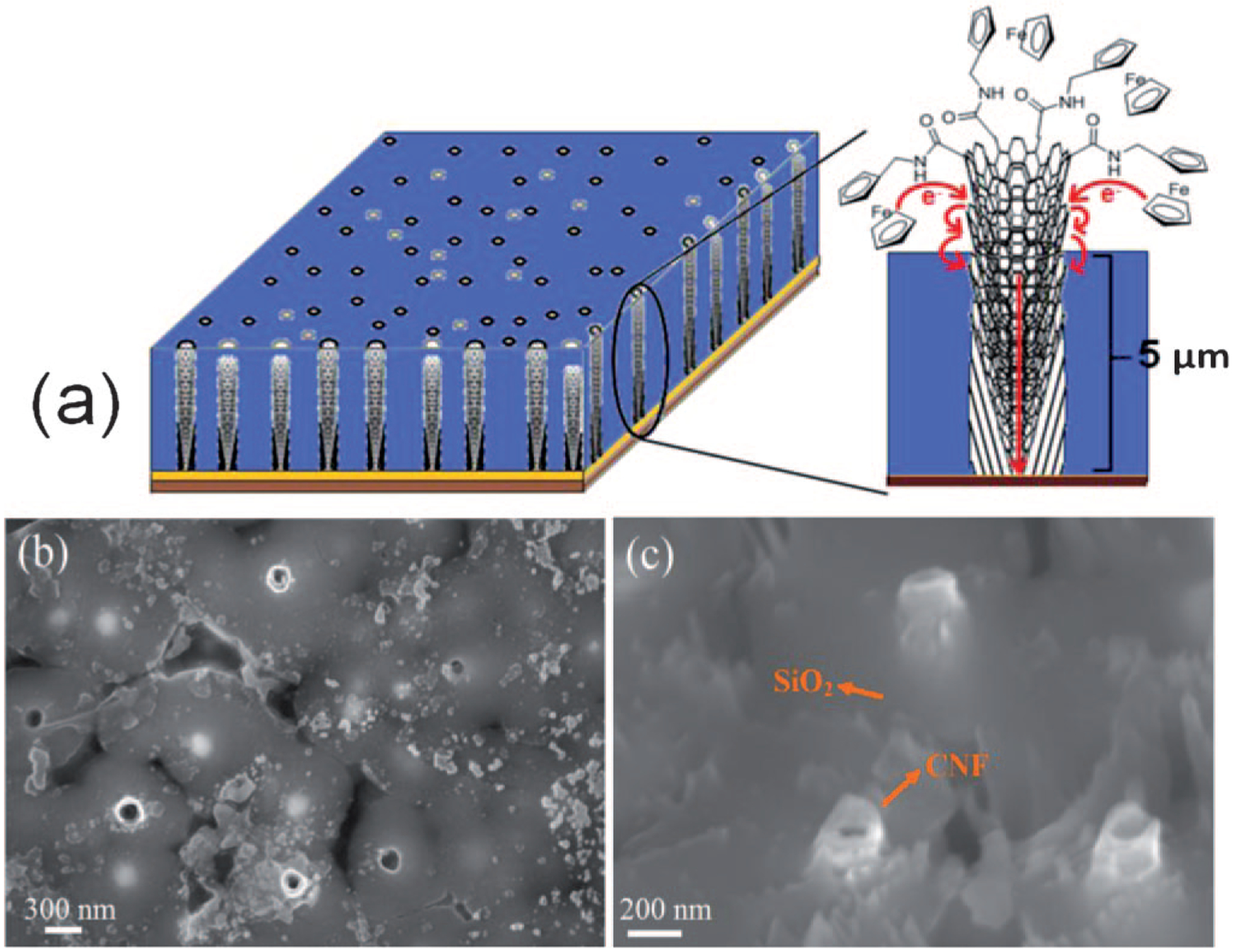
(a) Schematic of the embedded CNFs functionalized with ferrocene molecules at the exposed tip. The bottom brown color represents Si wafer, yellow color represents Cr contact layer under CNFs, blue color represents dielectric SiO2 deposited using TEOS CVD to encapsulate individual CNFs, dark black circle represents exposed CNF tips and grey circles represent the unexposed CNF tips buried in SiO2 matrix. Ferrocene moieties are functionalized to the tip and the sidewall of the exposed CNFs. (b) and (c) show top and 45° perspective views of scanning electron microscopic images of embedded CNFs with the scale bars of 300 and 200 nm, respectively.
As a first step to understand the electrochemical properties of the CNF NEA, we measured the DC CV with non-functionalized electrodes at a series of scan rates (v) in a bulk redox solution, i.e. 1.0 mM K4Fe(CN)6 in 1.0 M KCl solution. The CNF NEA displayed sigmoidal feature indicating the formation of a steady diffusion layer, which was also observed in previous studies [10]. The limiting current (il) derived from the step height was almost invariant with the scan rate. These characteristics confirm that the embedded CNFs behave as a low-density NEA.
Towards understanding the ETR, we first measured DC CVs at various scan rates with a GCE and a CNF NEA in 1.0 M KCl after FcCH2NH2 was covalently attached to the carboxylic acid groups at the carbon surface. As shown in Figure 2a, a set of redox waves on top of the flat non-faradic background currents are obtained with the GCE. The peak separation ΔEp was ~29 mV at 20 mV/s scan rate, indicating a quasi-reversible surface redox reaction with a relatively high ETR. The CV of Fcfunctionalized CNF NEA demonstrated similar features but with a much larger peak separation ΔEp≈81 mV at 20 mV/s scan rate (Figure 2b). Apparently, the ETR of Fc at CNF NEA is much lower than that at GCEs, evident by the larger ΔEp, specially at high scan rates (see Supporting Information Figure S4). Despite the difference in ETR, the peak current increases as the scan rate rises for both GCE and CNF NEA.
Fig. 2.
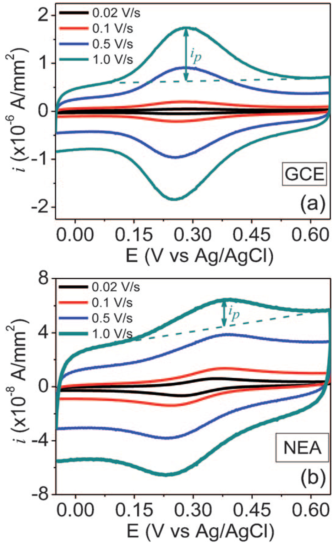
(a) and (b) Cyclic voltammetry measurements of Fcfunctionalized GCE and CNF NEA in 1.0 M KCl, respectively. Each set of measurements was performed at a series of scan rates of 0.020, 0.10, 0.50, and 1.0 V/s. The oxidation and reduction currents were normalized to the geometric surface area defined by the 3-mm i.d. O-ring.
Interestingly, the CV of Fc-functionalized CNF NEA in Figure 2b shows a unique tilt baseline which can be subtracted by a linear fitting as indicated by the dashed line. We have confirmed that this is not due to the solution resistance since the non-functionalized CNF NEAs in 1.0 M KCl show normal flat rectangular shape without such large tilting (see Supporting Information, Figure S3). The explanation of the tilting in baseline in the faradaic processes at CNF NEA is not clear at this point.
The surface coverage (Γo) of Fc on GCE and CNF NEA can be calculated using CV curves in Figures 2a and 2b by:
| (1) |
where Q is the integrated charge under the peak area of the anodic or cathodic wave and n=1 is the number of electrons involved in the redox reaction of each Fc [28]. The derived surface coverage of Fc is Fc/cm2 for GCEs, corresponding to 0.22 closely packed monolayer [15]. At the CNF NEA, it drops to 9.21 × 10¹¹ Fc/cm2, ~120 times lower than that on the GCE, corresponding to ~4.9 × 10⁴ Fc/CNF. The number of Fc molecules at each CNF is ~4.5 times higher than that in our previous study [10] due to the longer exposed CNF tip by selective RIE. Reliable signals were obtained even though the Fc coverage was only ~0.0018 monolayer of the geometric surface area.
Figure 3a summarizes the amplitude of background-corrected peak current (ip) vs. the scan rate (v) of the Fc–functionalized GCE and CNF NEA. The plot of the same data in log-log scale is shown in Figure 3b. The macro-GCE gives ip α vb with b=0.95, close to the theoretical value of 1. This is in perfect agreement with the theory of a nearly reversible surface redox reaction. For the Fc–functionalized CNF NEA, the peak current ip should also be linearly proportional to u, similar to that of the macro-GCE. However, to our surprise, Figure 3b gives b=0.38, much lower than 1. This anomalous behavior in CV of Fc-functionalized CNF NEA is likely attributed to the slow ETR which cannot catch up with the high scan rate. This would severely limit CNF NEAs for ultrahigh sensitivity and temporal resolution.
Fig. 3.
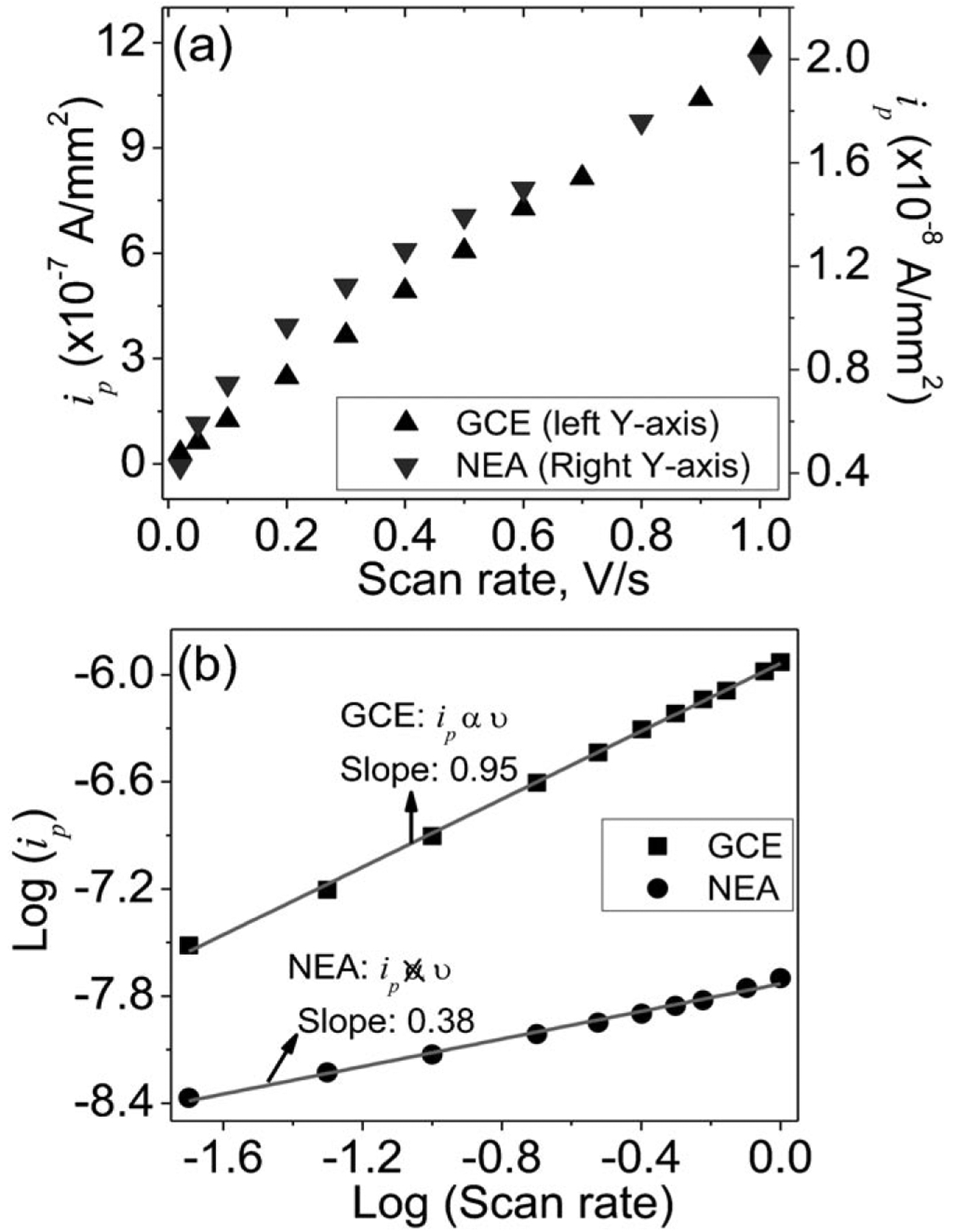
(a) The plots of background corrected peak currents (ip) derived from the CVs in Figure 2 of Fc-functionalized GCE and CNF NEA in 1.0 M KCl. (b) Plot of logarithm of (ip) vs. logarithm of the scan rate, the solid lines are the linear fitting curves by equation log(ip)=a+b log(v) with the slope b=0.95 for GCE and b=0.38 for CNF NEA.
Interestingly, ACV demonstrated dramatically different ETR from DC CV measurements. An anomalously high ETR at CNF NEAs was obtained comparing to GCEs. ACV has been previously employed to study redox kinetics in monolayers of FcCONH(CH2)15SH on Au electrode surfaces [16]. Higher current signal was obtained in ACV due to the fact that the electrons were cycled at each Fc by the sinusoidal AC wave superimposed on the linear DC potential ramp [16, 29], but the ETR was found to be the same by CV (k0=10 s−1) [33] and ACV (k0= 9–13 s 1) [29], in contrast to our results.
As shown in Figure 4, a peak AC current ip,ac corresponding to the redox reaction of surface-attached Fc is observed at +0.275 V for both GCEs and CNF NEAs. However, the dependence of ip,ac on the frequency of the applied AC voltage is dramatically different between these two types of electrodes. In Figures 4a–c, ip,ac at the GCE is very low (~8×10⁻⁷ A/mm2) at the starting frequency of 10 Hz. It increases by ~3.25 times to a maximum of ~2.6×10⁻⁶ A/mm2 as the frequency is raised to 75 Hz and then decreases until diminishes relative to the background as the frequency is raised to 3500 Hz. In contrast, as shown in Figures 4d–f, ip,ac at the CNF NEA starts at a much lower value of ~1×10⁻⁸ A/mm2 but continuously increases as the frequency is raised until reaching the maximum of ~2.8×10⁻⁷ A/mm2 at 3500 Hz. It slowly decreases as the frequency is further increased (see Figure 5). A substantial signal over the background (see Supporting Information, Figure S5a) is still measurable even at 10000 Hz, the maximum frequency that can be applied by the potentiostat (Model CHI440A, CH Instruments).
Fig. 4.
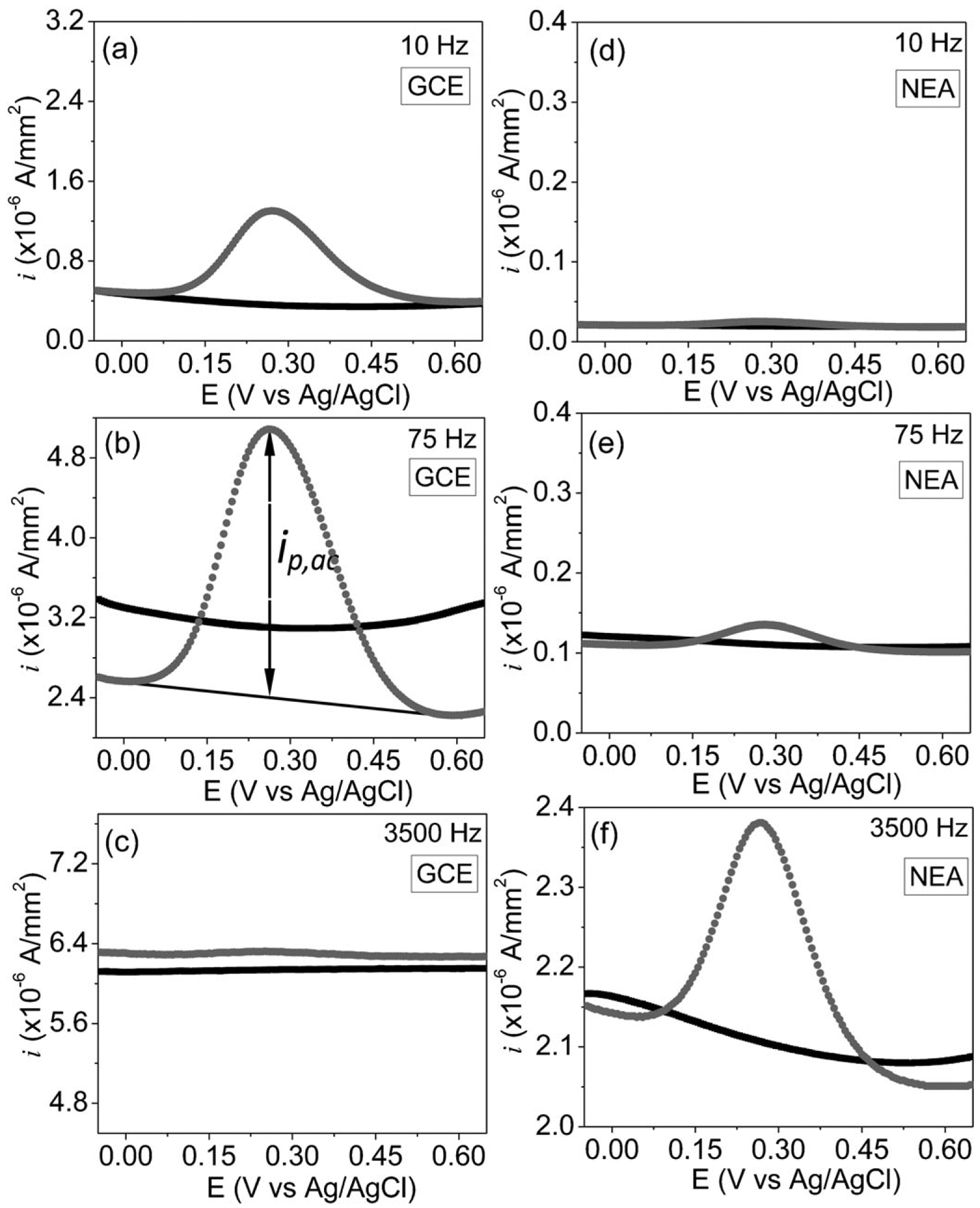
(a)–(f) AC voltammograms measured at 10, 75, 3500 Hz with a sinusoidal wave of 25 mV in amplitude superimposed on the DC staircase ramp from −0.05 to 0.65 V at a scan rate of 10 mV/sec. (a)-(c) are measurements on a Fc-functionalized GCE electrode, (d)–(f) on a Fc-functionalized CNF NEA. The black curves are the background currents measured with clean GCE and CNF NEA electrodes without Fc attachment in 1.0 M KCl and grey dotted curves are the ACV signals in 1.0 M KCl after functionalization of electrodes with Fc.
Fig. 5.
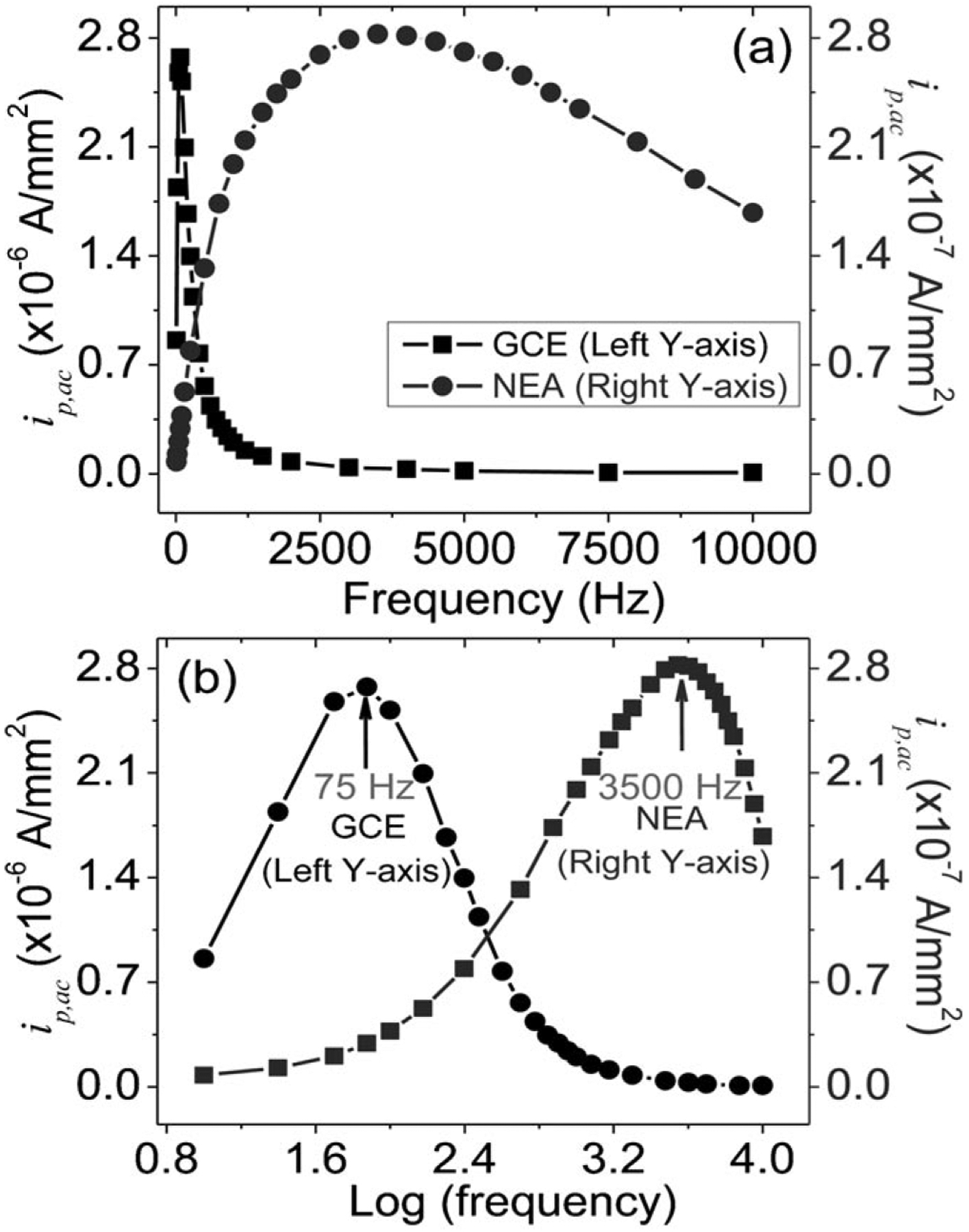
(a) Background corrected peak currents (ip,ac) of surface-attached Fc molecules in AC voltammetry vs. the frequency for the Fc-functionalized GCE and CNF NEA, respectively. The maximum ip,ac is at 75 Hz for the GCE whereas at 3500 Hz for the CNF NEA. (b) The same data plotted in log–log scale.
Within the proper frequency range, the peak AC current (ip,ac) can be used to estimate the surface coverage as described by Creager et al. [16] by:
| (2) |
where Γo is the surface coverage of Fc, f is the frequency, and ε is the peak amplitude of the superimposed AC voltage. From the measurements at 100 Hz with an amplitude of 25 mV, we obtained Γo=1.03×10¹³ Fc/cm2 for the GCE and Γo=3.09×10¹⁰ Fc/cm2 for the CNF NEA. These values are lower than those calculated from DC CV measurements similar to previous studies [16, 29]. Deviation from the theoretical prediction may be likely due to the slow ETR in this quasireversible system. While the DC based CV measurements at slow scan rates is more reliable in deriving the Fc coverage, ACV provides much larger peak current which is useful in improving the detection sensitivity in electroanalysis.
The difference between GCE and CNF NEAs in frequency dependence using ACV is more strikingly presented in Figures 5a and 5b, where the peak AC current (ip,ac) of the surface-functionalized Fc is plotted versus the frequency in linear and logarithm scales, respectively. The GCE shows a sharp peak in linear scale with the maximum ip,ac at 75 Hz while the CNF NEA presents a much broader peak with the maximum ip,ac at 3500 Hz. In logarithm scale, both GCE and CNF NEA show similar shape. Creager et al. [16, 29] reported that, as the frequency of the superimposed sinusoidal wave is over certain value, the ACV signal (i.e. ip,ac) diminishes because the ETR cannot cope up with the rapidly changing potential and is ultimately limited by the kinetics of the electrochemical reaction. Since CNF NEA reaches the maximum peak current at a much higher AC frequency than the GCE (i.e. 3500 Hz vs. 75 Hz), the ETR at the CNF NEA should be much higher than that at the GCE. This observation seems to contradict the above-discussed DC CV study which shows lower ETR at the CNF NEA. The puzzled difference between ACV and DC CV studies is probably associated with different mechanisms of electron transfer through the CNF NEA, which has not been studied before. This triggered us to reexamine the ETR constant k° using the DC CV data for both GCE and CNF NEA and to compare them with ACV results.
The ETR constant k° in literature is generally calculated from the DC CV data by a method described by Laviron [31], where the peak separation ΔEp at different scan rates (u) from CV curves is correlated by a dimensionless rate constant m=(RT/F)(k0/nv). For reactions with ΔEp below 200 mV, m can be readily derived from experimentally measured ΔEp from Laviron’s working curve between m−1 and nΔEp [32]. The k° values can then be calculated from m, which are 6.32 s−1 and 0.38 s−1 for GCE and CNF NEA functionalized with the Fc moiety at v=0.10 V/s, respectively (see Table 1). The k° of the GCE by DC CV is ~17 times higher than that of the CNF NEA. This is reflected by the difference in ΔEp (i.e. 177 mV for the CNF NEA vs. 25 mV for the GCE).
Table 1.
Surface coverage of Fc moiety and the k° calculated from the cyclic voltammetry data obtained at a scan rate of 0.10 V/s.
| Electrode | Γo (Fc/cm2) | E1/2 (mV) [a] | ΔEp (mV) | k° (S−1) |
|---|---|---|---|---|
| GCE | 1.1 ×10¹⁴ | 269 | 25 | 6.32 |
| CNF NEA | 9.2 ×l011 | 323 | 177 | 0.38 |
The potential is reported vs Ag/AgCl (sat’d KCl).
In a recent report, Landis et al. [27] studied Fc molecules attached through linkers of various lengths to the whole sidewall surface of a bare VACNF array with the average CNF length of 1.0 ±0.3 μm. The ΔEp was found to be ~50 mV at 100 mV/s scan rate and invariant while the linker molecule is changed from (CH2)3 to (CH2)10.The calculated ETR constant is k°≈ 1.2 s–1, which is slightly higher than our results on embedded CNF NEA but much lower than that on the GCE. Notably, in that study, the k° value is an average of the Fc molecules from proximal end to the distal end of the CNF. The ETR from the distal end is likely not limited at the Fc/CNF interface but by the intrinsic processes interior of CNFs. With these observations, we hypothesize that, in DC CV measurements with our embedded CNF NEAs, the electron from Fc has to hop between graphitic layers stacked along the 5 μm long CNF axis, leading to the low k°. This is analogous to the phenomena observed by Choi et al. [18] with long conductive molecular wires over ~4 nm. The slightly higher ETR constant in Landis’ study [27] is likely due to the fact that the average distance that electrons travel through the CNF is shorter in their case.
For ACV, we hypothesize that the capacitive coupling between the graphitic layers in the CNF is the dominant admittance mechanism. The measured capacitance at the CNF NEA generally involves two capacitors in series, i.e. (1) the interfacial capacitance (Cdl) due to the electric double layer between the electrolyte and the exposed CNF surface, and (2) the space charge capacitance (Csc) inside the conical graphitic layers stacked along the CNF axis. The exposed CNF surface can be treated as a mixture of basal and edge plane. It has been reported that the interfacial capacitance between electrolyte and basal plane graphite show a V-shape curve vs. electropotential, with a minimum value of ~10–20 μF/cm2 in aqueous solution while that of edge plane goes up to 70 μF/cm2 [33]. Previous study with HOPG electrodes only observed the interfacial capacitance Cdl since the CSC of HOPG is much larger [33]. Recently, by using a single-layer graphene in contact with ionic liquids and aqueous solutions, the total measured capacitance was found to be ~5–8 μF/cm2, which was dominated by the capacitance of the electrode materials and was attributed to the quantum capacitance CQ of the graphene [22]. But so far the understanding of the capacitance in the stacked graphitic layers in more complicated CNF structure is very limited. A recent study using a stack of controlled number of graphene layers [34] has provided some insights. As the number of graphene layers in the stack increases from 1 to 120, the measured capacitance was found to quickly increase to approach bulk graphite properties. Since there are much more than 120 graphene layers in a 5 μm long CNF, the interior capacitance of CNFs (CCNF or Csc) will be much larger than the interfacial capacitance Cdl. This large interior capacitance of CNFs creates a new electron transfer pathway through capacitive admittance defined by 2πfCCNF. Clearly, this new mechanism particularly favors high-frequency AC techniques since the admittance is proportional to the frequency (f). As a result, the measured ETR in ACV becomes limited by the interfacial faradaic process in contrast to that by the slow hopping process interior of CNFs in DC CV.
Another possibility is that the oxidation of Fc to ferrocenium converts Fe2+ to Fe3+, which may induce charging or structural change in the Fc monolayer that may hinder the ETR. The fast sinusoidal AC voltage may avoid this and give higher ETR. However, considering the small surface coverage (~0.22 monolayer) and high salt concentration in supporting electrolyte (1.0 M KCl) as well as the fact that the ETR by ACV is only slightly higher than DC voltammetry in measuring Fc-functionalized Au electrodes, the effect of surface structure is expected to be small.
In a deeper view, the RCNF and CCNF components along the CNF could behave as a microstructural electrical network consisting of randomly mixed capacitors and resistors similar to the microporous system studied by Almond et al. [35]. At the frequency that the capacitive admittance 2πfCCNF is comparable to or larger than the conductance of the resistive elements (i.e. RCNF−1), AC currents flow across the CNF via a complex set of paths with both capacitive and conductive components contributing to the network conductivity. This is in contrast to the DC or low-frequency AC currents, where the capacitors are essentially insulators, leaving the hopping paths through the resistive elements alone to determine the network response. To our knowledge, this is the first experimental discovery to indicate that a single nanowire conductor behaves as an electrical network due to its unique microstructural heterogeneity.
To assess the ETR in ACV, EIS was carried out from 100 kHz to 0.1 Hz with Fc-functionalized GCEs and CNF NEAs at a fixed DC potential bias corresponding to the peak potential for Fc in ACV (i.e. at +0.275 V). The EIS of Fc-attached GCE and CNF NEA have drastically different features (see Figure 6) and have to be fit with different equivalent circuits using a complex nonlinear least-squares package (Princeton Applied Research, TN). For the GCE, the equivalent circuit is slightly modified from the Randles circuit used in previous study of an electroactive monolayer on Au [29]. A resistor RL attributed to the leakage current has to be added in parallel with the pseudocapacitor Cads corresponding to the faradaic process of the surface adsorbed Fc (as validated by the difference in the fitting quality of the Bode plot in Figure 6c). This is likely because no passivation was used on the GCE to block the leakage current unlike the study on Au surface [29]. For the CNF NEA, the intrinsic properties of the ~5 μm long CNF CNF is represented by a capacitor CCNF in parallel with a resistor RCNF (see Figure 6b), which is necessary for obtaining a good fit to the EIS data, particularly to the two maxima in the Bode phase plot (see Figures 6d and Supporting Information Figure S8c). The fitting parameters for both electrodes are listed in Table 2.
Fig. 6.
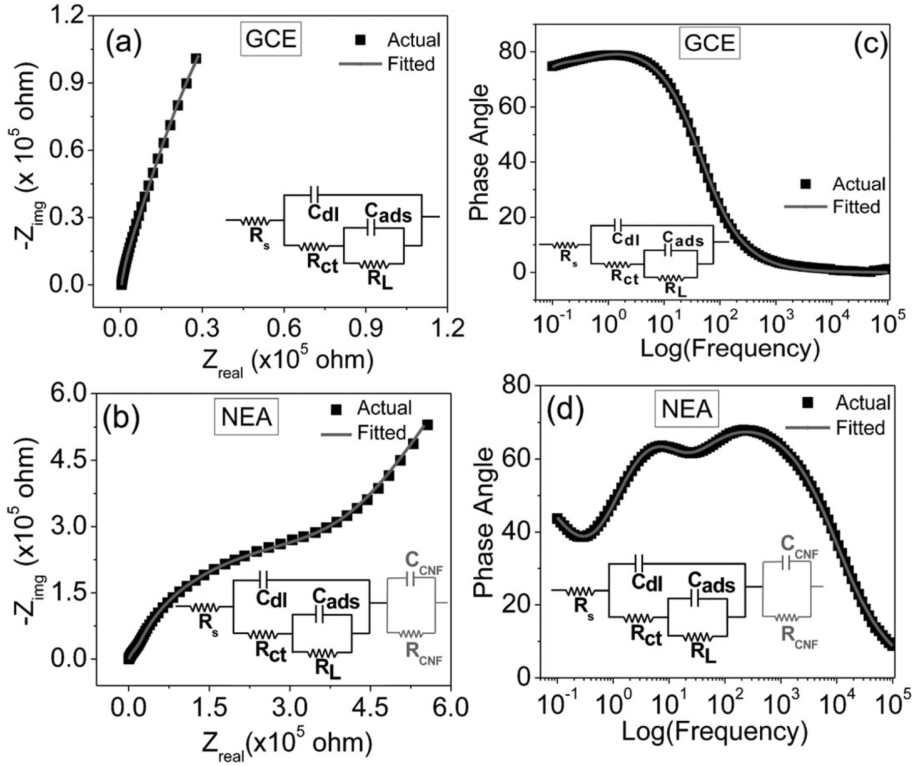
(a) and (b) Nyquist plots of the electrochemical impedance spectra of Fc-functionalized GCE and CNF NEA in 1.0 M KCl. The spectra were recorded at 20 mV voltage amplitude, 0.1 Hz to 100 kHz frequency range, and biased at a DC potential of +0.275 V vs. Ag/AgCl (sat’d KCl). (c) and (d) are the bode plots (phase angle vs. log (frequency)) of the same experiment. The grey solid line is the fitting curve obtained by using the equivalent circuits shown in insets. The fitting parameters are listed in Table 2.
Table 2.
Fitting parameters for the electrochemical impedance spectra of Fc-attached electrodes and derived AC ETR constant k0ac.
| Electrode | Rs (Ω) | Cdl (F) (n) | Rct (Ω) | Cads (F) (n) | RL (Ω) | Ccnf (F) (n) | RCNF, (Ω) | k°ac (S−1) |
|---|---|---|---|---|---|---|---|---|
| GCE | 412.6 | 1.26×10⁻⁵ (0.93) | 2.37×10⁵ | 3.45× 10⁻⁶ | 5.57×10⁴ | – | – | 0.61 |
| CNF NEA | 311.3 | 4.14×10⁻⁷ (0.864) | 5.17×10⁴ | 2.55×10⁻⁷ (0.976) | 2.62×10⁵ | 2.49×10⁻⁶ (0.707) | 2.95× 10⁷ | 38.0 |
Note: If a number in the bracket is given below a capacitor, it indicates that a constant phase element (CPE) is used instead of an ideal capacitor and the number represents the value of the exponent n of the CPE.
The values of the fitting parameters from the EIS can be used to estimate the ETR constant for surface-attached redox species in ACV by:
| (3) |
where Rct is the charge transfer resistance and Cads is the pseudocapacitance by surface-adsorbed redox species [29]. For fitting purpose, the capacitors were replaced by the constant phase elements (CPEs) following the general practice to account for the heterogeneity at the electrode surface [16, 29]. CPE is defined by the relationship ZCPE=1/(C(iω)n) where C is the capacitance, ω is the angular frequency and n is a dimensionless exponent whose value range from 0 to 1 [36]. The ETR constants k°ac calculated by Eq. 3 using the fit values of Rct and Cads (see Table 2) are 0.61 s–1 for GCE and 38.0 s–1 for CNF NEA, respectively. Apparently, the k°ac value for the CNF NEA is about 62 times of that of the GCE. The equivalent circuit to fit the EIS of CNF NEAs is very consistent with our above-discussed electron transfer mechanism in ACV. Both the resistive conductance and capacitive admittance contribute to the current flow. The fitting value of RCNF is very high (2.946×10⁷ Ω). Thus even a low AC frequency f=2.17 mHz is sufficient to make the capacitive admittance equal to the resistive conductance, namely 2πfCCNF=1/RCNF. Since the EIS was taken from 0.1 Hz to 100 kHz, the capacitive admittance is much larger than the resistive conductance in this range. Little current flows through RCNF. As a result, dropping RCNF by using CCNF alone can generate the same fitting quality (see Supporting Information Figures S7b,d). The fitting values of Rct and Cads are only slightly changed, which give almost the same value of ETR constants, i.e. k°ac=38.1 s–1.
Even though much higher ETR has been obtained with ACV, it is not conclusive whether the measured ETR with AC voltammetry is still limited by CNF interior structure or limited by the heterogeneous electron transfer at the Fc-CNF interface. By combining our results with the study by Landis et al. [27], it is likely that the interior structure of CNFs is still the limiting factor. But this may be sufficient for biosensing applications to detect many biomolecules which have much slower ETRs than Fc. For very slow ETR reactions, we may obtain the same ETR value by DC and AC voltammetry, if it is measurable.
4. Conclusions
In summary, distinct ETRs by AC and DC voltammetry for Fc molecules covalently attached at the distal end of embedded CNF NEAs. In DC CV measurements, the ETR at CNF NEAs is about 17 times lower than on GCE. However, in ACV, the ETR at the CNF NEA is 62 times higher than that on GCEs. The high ETR at CNF NEAs by ACV is reflected in the capability to obtain the maximum peak current of Fc at 3500 Hz in CNF NEAs vs. at ~75 Hz in GCEs. The difference is likely due to the microstructure of the unique conically stacked graphitic layers in CNFs, which can be treated as a microstructural electrical network with randomly mixed resistive and capacitive pathways. This model is consistent with the equivalent circuits of EIS. The understanding of these phenomena will provide new insights into the fundamental electronic properties of nanostructured carbon materials and stimulate the development of high-performance biosensors and nanoelectronics.
Supplementary Material
Acknowledgement
JL thanks Kansas State University and Early Warning Inc. for financial support. Part of this work was supported by Grant Number P20RR015563 from the National Center for Research Resources and Grant R15CA15921-0-01 from NIH. We thank Dr. Daniel Higgins for helpful discussions.
Footnotes
Supporting Information for this article is available on the WWW under http://dx.doi.org/10.1002/elan.201100088.
References
- [1].Penner RM, Heben MJ, Longin LT, Lewis NS, Science 1990, 250, 1118. [DOI] [PubMed] [Google Scholar]
- [2].Fan F-RF, Bard AJ, Science 1995, 267, 871. [DOI] [PubMed] [Google Scholar]
- [3].Menon VP, Martin CR, Anal. Chem 1995, 67, 1920. [Google Scholar]
- [4].Wei D, Bailey MJA, Andrew P, Ryhanen T, Lab Chip 2009, 9, 2123. [DOI] [PubMed] [Google Scholar]
- [5].Lapierre-Devlin MA, Asher CL, Taft BJ, Gasparac R, Roberts MA, Kelley SO, Nano Lett. 2005, 5, 1051. [DOI] [PubMed] [Google Scholar]
- [6].Li J, Koehne JE, Cassell AM, Chen H, Ng HT, Ye Q, Fan W, Han J, Meyyappan M, Electroanalysis 2005, 17, 15. [Google Scholar]
- [7].Tu Y, Lin YH, Yantasee W, Ren ZF, Electroanalysis 2005, 17, 79. [Google Scholar]
- [8].Baker SE, Tse KY, Lee CS, Hamers RJ, Diamond Relat. Mater 2006, 15, 433. [Google Scholar]
- [9].Arumugam PU, Chen H, Siddiqui S, Weinrich JAP, Jejelowo A, Li J, Meyyappan M, Biosens. Bioelectron 2009, 24, 2818. [DOI] [PubMed] [Google Scholar]
- [10].Li J, Ng HT, Cassell A, Fan W, Chen H, Ye Q, Koehne J, Han J, Meyyappan M, Nano Lett. 2003, 3, 597. [DOI] [PubMed] [Google Scholar]
- [11].Lin YH, Lu F, Tu Y, Ren ZF, Nano Lett. 2004, 4, 191. [Google Scholar]
- [12].Yu Z, McKnight TE, Ericson MN, Melechko AV, Simpson ML, Morrison B, Nano Lett. 2007, 7, 2188. [DOI] [PubMed] [Google Scholar]
- [13].McKnight TE, Melechko AV, Hensley DK, Mann DGJ, Griffin GD, Simpson ML, Nano Lett. 2004, 4, 1213. [Google Scholar]
- [14].Chidsey CED, Science 1991, 251, 919. [DOI] [PubMed] [Google Scholar]
- [15].Chidsey CED, Bertozzi CR, Putvinski TM, Mujsce AM, J. Am. Chem. Soc 1990, 112, 4301. [Google Scholar]
- [16].Creager S, Yu CJ, Bamdad C, O’Connor S, MacLean T, Lam E, Chong Y, Olsen GT, Luo JY, Gozin M, Kayyem JF, J. Am. Chem. Soc 1999, 121, 1059. [Google Scholar]
- [17].Sikes HD, Smalley JF, Dudek SP, Cook AR, Newton MD, Chidsey CED, Feldberg SW, Science 2001, 291, 1519. [DOI] [PubMed] [Google Scholar]
- [18].Choi SH, Kim B, Frisbie CD, Science 2008, 320, 1482. [DOI] [PubMed] [Google Scholar]
- [19].Ngo Q, Cassell AM, Austin AJ, Li J, Krishnan S, Meyyappan M, Yang CY, IEEE Electron Device Lett. 2006, 27, 221. [Google Scholar]
- [20].Zhang L, Austin D, Merkulov VI, Meleshko AV, Klein KL, Guillorn MA, Lowndes DH, Simpson ML, Appl. Phys. Lett 2004, 84, 3972. [Google Scholar]
- [21].Heller I, Mannik J, Lemay SG, Dekker C, Nano Lett. 2009, 9, 377. [DOI] [PubMed] [Google Scholar]
- [22].Xia JL, Chen F, Li JH, Tao NJ, Nat. Nanotechnol 2009, 4, 505. [DOI] [PubMed] [Google Scholar]
- [23].Baramee A, Coppin A, Mortuaire M, Pelinski L, Tomavo S, Brocard J, Bioorg. Med. Chem 2006, 14, 1294. [DOI] [PubMed] [Google Scholar]
- [24].Cruden BA, Cassell AM, Ye Q, Meyyappan M, J. Appl. Phys 2003, 94, 4070. [Google Scholar]
- [25].Ren ZF, Huang ZP, Xu JW, Wang JH, Bush P, Siegal MP, Provencio PN, Science 1998, 282, 1105. [DOI] [PubMed] [Google Scholar]
- [26].Melechko AV, Merkulov VI, McKnight TE, Guillorn MA, Klein KL, Lowndes DH, Simpson ML, J. Appl. Phys 2005, 97, 41301. [DOI] [PubMed] [Google Scholar]
- [27].Landis EC, Hamers RJ, J. Phys. Chem. C 2008, 112, 16910. [Google Scholar]
- [28].Bard AJ, Faulkner LR, Electrochemical Methods: Fundamental and Applications, Wiley, New York: 2001. [Google Scholar]
- [29].Creager SE, Wooster TT, Anal. Chem 1998, 70, 4257. [Google Scholar]
- [30].Weber K, Creager SE, Anal. Chem 1994, 66, 3164. [Google Scholar]
- [31].Laviron E, J. Electroanal. Chem 1979, 101, 19. [Google Scholar]
- [32].Finklea HO, in Electroanalytical Chemistry: a Series of Advances, Vol. 19, Marcel Dekker, New York: 1996, p. 109. [Google Scholar]
- [33].Randin JP, Yeager E, J. Electrochem. Soc 1971, 118, 711. [Google Scholar]
- [34].Wang DW, Li F, Wu ZS, Ren WC, Cheng HM, Electrochem. Commun 2009, 11, 1729. [Google Scholar]
- [35].Almond DP, Bowen CR, Phys. Rev. Lett 2004, 92, 4. [DOI] [PubMed] [Google Scholar]
- [36].MacDonald JR, Impedance Spectroscopy, Wiley, New York: 1987. [Google Scholar]
Associated Data
This section collects any data citations, data availability statements, or supplementary materials included in this article.