

Abstract
Layered lead-halide perovskites have shown tremendous success as an active material for optoelectronics. This is attributed to the electronic structure of the inorganic sublattice and large exciton binding energies due to quantum and dielectric confinement. Expanding functionalities for applications that depend on free-carrier generation requires new material design routes to decrease the binding energy. Here we use electronic structure methods with model Bethe–Salpeter equation (BSE) to examine the contributions of the dielectric screening and charge-transfer excited-states to the exciton binding energy of phenylethylammonium (PEA2PbBr4) and naphthlethylammonium (NEA2PbBr4) lead-bromide perovskites. Our model BSE calculations show that NEA introduces hole acceptor states which impose charge-transfer character on the exciton along with larger dielectric screening. This substantially decreases the exciton binding compared to PEA. This result suggests the use of organic cations with high dielectric screening and hole acceptor states as a viable strategy for reducing exciton binding energies in two-dimensional halide perovskites.
Keywords: Exciton, Binding Energy, Charge Transfer, Perovskite, Dielectric
Two dimensional (2D) organic–inorganic Ruddlesden–Popper lead halide perovskites (A’)2(A)n−1PbnX3n+1 where [A = Cs+, CH3NH3+, HC(NH2)2; A’ represents variable spacer cations; X = Cl,Br,I; n is layer thickness], have shown considerable success for optoelectronic applications including photovoltaics,1−3 light-emitting diodes,4 and photodetectors in the UV–vis and X-ray5−8 regime. These classes of materials can be tuned physically or chemically. The latter is achieved by changing the halide content and/or the organic cation species that separate the inorganic 2D layers and adjust the physical interlayer distance of the 2D layers. Changes in the halide content affect the fundamental bandgap where iodide (chloride) provides the smallest (largest) gap.9 The optical gap can also be altered by the layer thickness,10 which changes the confinement potential and consequently the exciton binding energy. There are fundamental limits on increasing the thickness of the inorganic layer in 2D perovskites.11 Based on the limited tunability of the inorganic layer, there is a motivation to explore modifications of the organic spacer cations for engineering the desired photophysical properties.
One important quantity to control in these materials is the exciton binding energy. For LED applications, it is desirable to increase the exciton binding energy as it increases the radiative decay rate, whereas for photovoltaics and photodetectors, it is desirable to decrease the binding energy to reduce the barrier for exciton dissociation into free charge carriers. For monolayer materials, the electric field lines of the bound exciton penetrate outside the inorganic component into the organic layer. This offers a route to modulate the exciton binding energy via dielectric confinement.12 One approach is to tune the dielectric screening in the perovskite 2D layer with the choice of organic cation.13,14 Choosing suitable organic molecules with polar functional groups, such as enthanolamine,15,16 has shown to increase the dielectric screening of the organic layer thus reducing the binding energy. An alternate strategy for diminishing dielectric screening involves the doping of electron-donating pairs that interact with electron-accepting organic layers resulting in a reduction of the exciton binding energy.17 An alternative path for generating free-carriers was directly exciting electron donor–acceptor pairs within the organic layer which subsequently transfer carriers to the inorganic layer.18,19
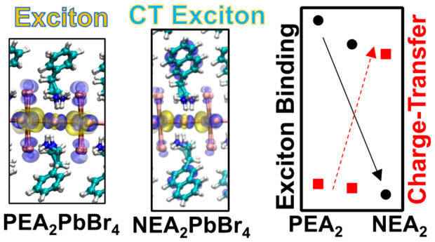
This study supports an alternative strategy to lower the exciton binding energy. This involves regulating the electronic coupling between the inorganic and organic layers through strategically aligned donor–acceptor energy offsets. If the 1s exciton of the inorganic layer can couple with a hole or electron accepting unit from the organic layer, it is roughly anticipated that the binding energy will decrease by their energetic offset. One of the earliest studies focused on enhancing the coupling between the inorganic perovskite layer and the organic layer involved the utilization of naphthyl-ethylammonium (NEA). NEA contains two fused conjugated phenyl groups, which in principle should lower the band gap of the organic layer relative to PEA and provide larger electronic coupling at the inorganic–organic interface. It was observed that for NEA2PbBr4 the inorganic monolayer sensitizes the NEA organic layer, which manifests as phosphorescence below the optical gap of the perovskite layer.20−23 Initial reports attributed the sensitization pathway to triplet energy transfer,24 but recently it has been proposed that sensitization of the acceptor intralayer NEA occurs via a two-step process with the first step being interfacial hole charge-transfer.25 The concept of excitons with charge-transfer character in these materials is interesting as it could provide a pathway for decreasing the exciton binding energy.
Computational modeling can assist in understanding the relationships between structure of the spacer cations and the photophysical properties of these materials. Modeling has provided insights into the effects of spacer cations, and organic ligands in general, on the nonradiative charge-carrier dynamics, including carrier lifetimes26,27 and decoherence,28−30 relative energetics of organic layers to the inorganic layer,31−33 optical properties,34−36 and defect tolerence,24,37,38 have been gained through simulations based on density functional theory (DFT). For the case of using electronic structure methods to compute excitons and their binding energy in periodic solids, the use of additional methods for light-matter interactions, such as linear response time-dependent DFT or the many-body approach of the Bethe–Salpeter equation (BSE), is required. In the Supporting Information Methods section, we introduce a parametrized version of the BSE known as model BSE (mBSE) where the dielectric screening is approximated as a model with material dependent parameters. This reduces the computational cost of converging the exciton binding energy on dense reciprocal space grids, which can be computationally intractable for models of this size using the GW0 approach while maintaining qualitative agreement in computed optical properties to the BSE.
We then use the DFT electronic structure in combination with mBSE calculations, verified against its more accurate counterpart in a limited reciprocal space sampling, to explore the energetic alignment of excitonic and charge-transfer excitations in PEA2PbBr4, PEA1.5NEA0.5PbBr4, and NEA2PbBr4 lead halide perovskite crystals, which are shown in Figure 1. From the computed band structures, we first deduce that PEA2PbBr4 shows a direct bandgap at the Γ point with contributions from the [PbBr4]2– layer. Upon incorporation of NEA, we find that valence band states are introduced close to the gap of the inorganic layer in the case of PEA1.5NEA0.5PbBr4. Additionally, a hole-acceptor state emerges inside the inorganic gap for NEA2PbBr4. We then compute optically active excited-states using the mBSE approach. The results demonstrate blue-shifts for PEA1.5NEA0.5PbBr4, and NEA2PbBr4 relative to that for PEA2PbBr4 which are attributed to the increased static dielectric constant. The charge-transfer character of significant excited states is then characterized by the change in charge-density from the valence and conduction transition weighted by the mBSE amplitudes. We find that the lowest energy exciton in NEA2PbBr4 exhibits significant charge-transfer character, originating from the hole-acceptor state at the Γ point. Consequently, the computed exciton binding energy is reduced significantly in the NEA2PbBr4 monolayer compared to that in PEA2PbBr4 due to the coupling to the hole acceptor state along with the increased dielectric screening of the NEA organic layer. This illustrates that identifying organic components capable of delivering enhanced dielectric screening and introducing charge-transfer character can decrease exciton binding in 2D lead-halide perovskites.
Figure 1.

Atomistic structures in their unit cells for (a) PEA2PbBr4, (b) PEA1.50NEA0..50PbBr4, and NEA2PbBr4.
The atomistic structure file NEA2PbBr4 was obtained from Du et al.39 Starting from this structure, the naphthalene units are manually modified to obtain PEA2PbBr4. A (NEA)0.50(PEA)1.5PbBr4 alloyed structure is obtained by leaving one NEA molecule in place when modifying the structure to PEA. The obtained structures and unit cells are then optimized for each of the models, as described in the Supporting Information Methods. The resulting structures as shown in Figure 1 (a) PEA2PbBr4, (b) (NEA)0.50(PEA)1.50PbBr4, and (c) NEA2PbBr4, are used for further investigation of electronic structure and optical properties.
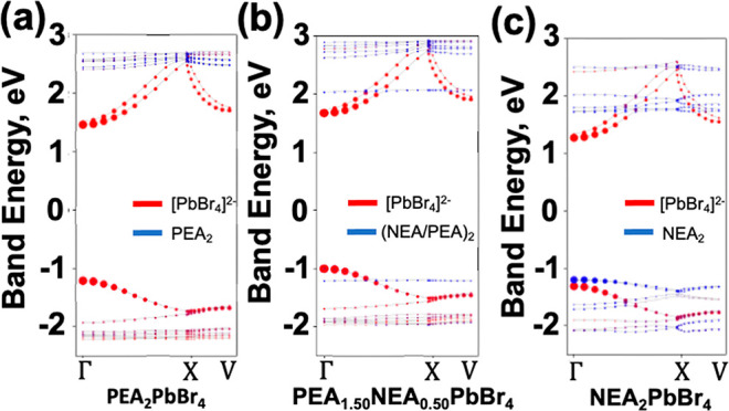
Using the optimized structures, we compute the electronic bands within the plane of the 2D inorganic [PbBr4]2– sublattice. Note that the out-of-plane dispersion is flat, as shown in Supplemental Figure S1, avoiding the need to sample reciprocal space along those dimensions. Figure 2 shows the PBE computed band structure along the high symmetry points and the corresponding HOMO and LUMO charge densities at the Γ. Here we project the change density contributions for each band onto ions from the [PbBr4]2– or organic molecule sublattice in red and blue, respectively. For PEA2PbBr4, the direct bandgap at the Γ point is composed exclusively by the [PbBr4]2– sublattice with contributions of the PEA molecular sublattice higher in energy. This is illustrated by plotting the HOMO and LUMO orbitals at the Γ point with the charge density residing only on the [PbBr4]2– sublattice.
Figure 2.

Computed band structure along with HOMO and LUMO Kohn–Sham orbitals at the Γ point for (a)-(b) PEA2PbBr4, (c)-(d) PEA1.50NEA0..50PbBr4, and (e)-(f) and NEA2PbBr4. Simulations used the PBE functional along high-symmetry points in the plane of the 2D LHP. The red (blue) curves correspond to projected atomic contribution from the [PbBr4]2– (PEA2 or NEA2 organic layer).
Markedly, doping the organic PEA sublattice with the NEA molecule introduces new features into the band-structure, as shown in Figure 2(c). Specifically, two flat bands near −1 and 2 eV are attributable to the NEA molecule. The direct bandgap at the Γ point is still dominated by contributions from the [PbBr4]2– sublattice as shown by the HOMO and LUMO Kohn–Sham orbitals in Figure 2(d). The V-valley of the band-structure has charge transfer character, where the LUMO is localized on the [PbBr4]2– sublattice whereas the HOMO is located to the NEA molecule. When the organic sublattice is composed entirely of the NEA molecules, additional features of the band-structure emerge, as shown in Figure 2(e). Instead of a flat band across the Brillouin zone, the bands contributed by the NEA molecule gain dispersive character. This is attributed to the π–π stacking interactions facilitating delocalization of charge density along the in-plane direction of the organic sublayer. The stabilization induced by π–π stacking also places occupied bands of the NEA units inside the direct bandgap of the [PbBr4]2– sublattice at the Γ point, as shown by the Kohn–Sham orbitals in Figure 3(f). Stated differently, the HOMO of the NEA sublattice looks like a hole accepting state relative to the [PbBr4]2– sublattice at both the Γ and the V points. In the Supporting Information, we examine changes in the band-structure when considering functional choice and the inclusion of spin–orbit coupling. We find consistent agreement of the introduction of a hole-acceptor state inside the fundamental bandgap independent of method. Additionally, the computed bandstructures predicting a hole-acceptor state inside the fundamental gap of the inorganic layer for NEA2PbBr4 agrees with recent experimental finding of two-step sensitization from a hole transfer from the inorganic to organic layer.25
Figure 3.

Computed absorption spectrum, dielectric properties, and exciton characteristics for the three structures. (a) Absorption spectrum calculated at the mBSE@PBE level of theory on a 21 × 21 × 1 reciprocal space mesh for PEA2PbBr4 (red), PEA1.50NEA0..50PbBr4 (green), and NEA2PbBr4 (blue). (b) Static dielectric constant computed at DFTP level as described by ref 1 in the Supporting Information. (c) Estimated exciton binding energy (computed with SI eq 9, left axis, black circles) and charge-transfer character (computed with SI eq 11, right axis, red squares) for the lowest-energy exciton.
Next we examine how the acceptor state of the NEA organic layer inside the bandgap of the inorganic [PbBr4]2– sublattice affects the nature of excited-states in the material using the mBSE method. In the Supporting Information, we detail the convergence of parameters in the mBSE and comparison to BSE. Figure 3(a) shows the mBSE@PBE computed optical absorption spectrum for the three materials. The plot indicates consistent blue-shifts of the lowest energy exciton peak from PEA2PbBr4 to (NEA)0.50(PEA)1.50PbBr4 and to NEA2PbBr4. This is attributed primarily to the increasing of the static dielectric constant ϵs for this sequence, as opposed to structure changes of the inorganic lattice, which is shown to be negligible in Supplemental Figure S7. For PEA2PbBr4, we calculate an exciton binding energy of 511 meV, which is larger than measured value in recent experiments40 and estimates from the quasi-particle BSE@GW0 calculations,13 but falls within the range predicted by semiempirical models.41 When substituting a single NEA molecule into the unit cell, the exciton binding energy marginally decreases to 477 meV. However, for the NEA2PbBr4 case when all PEA are replaced with NEA the exciton binding energy decreases significantly to 249 meV. This is shown in Figure 3(c). This result indicates that the exciton is destabilized by an NEA2 organic layer. We hypothesize that an effective decrease of the Coulombic attraction between the photoinduced electron and hole is due to an increased dielectric screening of NEA2 compared to PEA2, as seen in Figure 3(b). To confirm this, we further evaluate the binding energy in the NEA2PbBr4 material when using the PEA2PbBr4 static dielectric constant. This provides a binding energy of 384 meV accounting for 124 meV of the total 262 meV difference in the exciton binding energy between PEA2PbBr4 and NEA2PbBr4. This indicates the presence of additional physical effects beyond dielectric screening that need to be considered to explain the exciton destabilization caused by the NEA2 organic lattice.
Since the NEA2PbBr4 has hole acceptor states inside the inorganic [PbBr4]2– sublattice bandgap, it is feasible that these states affect the lowest-excited state exciton by introducing some charge-transfer character. To quantify this, we next use Equations (S10)-(S11) from the Supporting Information as follows: First, for a given single-particle transition from the valence to conduction bands, we estimate changes in the electronic density Δρ from the inorganic lattice to the organic lattice. Here, positive values indicate charge transfer from the inorganic to organic lattices, and negative values suggest the opposite process. Second, we weight the density difference by the mBSE@PBE amplitude modulus square |Avck|2 for a given single-particle excitation. Finally, we sum all contributions to the exciton. This metric captures the contribution of optically bright charge-transfer excitations to the excitonic wave function. The obtained values are displayed in Figure 3(c) as red squares. It reveals that the lowest energy excitations in PEA2PbBr4 and PEA1.50NEA0.50PbBr4 have minimal charge-transfer characteristics, whereas NEA2PbBr4 demonstrates charge-transfer contributions that are an order of magnitude greater. In the Supporting Information, we examine how SOC impacts the computed charge-transfer metric with the main finding that the charge transfer character within the NEA2PbBr4 excitonic wave function remains consistent, regardless of whether SOC corrections are included or not, with minor changes between the other two models.
The role of the hole acceptor state in NEA2PbBr4 causing a reduction in the exciton binding energy is further explored in Figure 4, which showcases the contributions of the band to the exciton. The red and blue circles indicate the charge density residing on the inorganic [PbBr4]2– and organic layers, respectively. The radii of the circles are proportional to the mBSE@PBE computed amplitudes module squared |Avck|2 for each valence to conduction transition and at every reciprocal lattice point. For the PEA2PbBr4 exciton, shown in Figure 4(a), it is found that the exciton only has contributions from the inorganic [PbBr4]2– layer, primarily from the Γ point. In the case of the PEA1.50NEA0.50PbBr4 exciton depicted in Figure 4(b), a flat band emerges from the NEA molecules in the organic layer, yet this does not substantially contribute to the exciton. Subsequently, in the case of the NEA2PbBr4 exciton shown in Figure 4(c), we observe that the organic hole-acceptor state inside the inorganic [PbBr4]2– layer makes an equivalent contribution to the exciton at the Γ point. Since this hole acceptor state inside the gap contributes to the exciton, it is natural to assume that the exciton binding would subsequently decrease due to its occupation. This energy difference between the donor and acceptor bands at the Γ point is 111 meV. The combination of this energy difference and the dielectric screening contribution to the reduced binding energy explains the significant reduction in binding energy observed between the PEA2PbBr4 and NEA2PbBr4 perovskite structures.
Figure 4.
Band structure decomposed contribution to the 1s exciton computed at mBSE@PBE. The red (blue) circles correspond to the projected atomic contribution from the inorganic [PbBr4]2– (organic PEA2 or NEA2 layers) for (a) PEA2PbBr4, (b) PEA1.50NEA0.50PbBr4, and (c) NEA2PbBr4.
The main finding of this study is the characterization of the contributions from dielectric screening and charge-transfer character to the substantially reduced 1s exciton binding in the layered halide perovskite when substituting the organic layer from PEA to NEA. Tuning dielectric confinement effect in two-dimensional materials is a general concept12 that applies to any semiconducting 2D layer in a dielectric medium. Tuning dielectric constants though substitution of organic molecules has been studied experimentally15 and computationally.13 In Supporting Information Table S4, we report experimentally reported binding energies and static dielectric constants and detail how they compare the results of this work. We find that the concept of dielectric tuning for reduced exciton binding energies is clearly demonstrated in these works. The novel prediction in this work is the coupling of the exciton of the inorganic layer to acceptor states of organic layer leads to reduced binding energies. The contribution from charge-transfer character of the exciton by coupling to acceptor states inside the fundamental gap is a more surprising, yet intuitive, result. This approach is relatively less investigated compared to dielectric screening engineering, as it falls outside the conventional Wannier-Mott exciton model where the binding energy can be adjusted through the carrier’s effective masses and dielectric screening. There are also caveats for using this approach for generating free-charge carriers in the inorganic layer. For 2D NEA2PbBr4, the identification of a hole acceptor charge-transfer contribution to the exciton is consistent with experimental report of hole-transfer in sensitizing NEA;25 however, it is well established that the NEA triplet excitons become sensitized. Thus, it is desirable to explore molecules that can introduce additional hole accepting states inside the fundamental gap of the inorganic layer, which are, however, not accessible by sensitization. Design principles for discovering such molecules can be borrowed from the photovoltaic community with rich experience in optimal alignment of electronic bands at interfaces. Here we look at monolayer A2PbBr4 perovskites where charge-carriers experience strong spatial and dielectric confinement. Increasing the thickness off the inorganic layer to (A’)2(A)n−1PbBr3n+1, where n represents layer thickness, would reduce the spatial confinement and consequently the exciton binding energy. This route can also be explored in conjunction with dielectric tuning and charge-transfer coupling to the organic-layer, but imposes synthetic and stability challenges in terms of crystal uniformity and reduced thermodynamic stability, respectively.11
In conclusion, two-dimensional lead halide perovskites (A’)2(A)n−1PbnX3n+1 exhibit considerable potential for various optoelectronic applications. However, in order to enhance their suitability for applications reliant on free-carrier generation, such as photovoltaics and photocatalysis, it is imperative to develop methods for substantial reduction of the exciton binding energy in these materials. In this study, we employ atomistic electronic structure simulations to investigate the exciton binding energy in a representative monolayer halide perovskite PEA2PbBr4, and examine the impact of substituting the PEA molecules with NEA. To compute the exciton binding energies, we use a model dielectric function to account for Coulombic screening in a combination with the Bethe–Salpeter equation. When fully substituting NEA in the unit cell, we observe a significant reduction in the binding energy from 511 to 249 meV for PEA2PbBr4 and NEA2PbBr4, respectively. We further delineate two main contributions to the reduced binding energy. First, we find that NEA within the perovskite lattice yields a higher static dielectric constant compared to PEA. This results in increased Coulombic screening of the exciton. Second, the NEA organic layer introduces hole-acceptor states at the Γ point inside the bandgap of the inorganic [PbBr4]−2 layer. These hole-acceptor states impose a significant charge-transfer character to the exciton, further contributing to the reduction in binding energy. Overall, this underscores the incentive to investigate organic components that increase the dielectric screening and introduce hole-acceptor states inside the gap, as potential avenues for diminishing exciton binding energy to facilitate the generation of free-carriers.
Acknowledgments
A.F. thanks Filipp Furche and Carsten Ullrich for comments and discussions during development of this manuscript. The work at Los Alamos National Laboratory (LANL) was supported by the LANL LDRD program (A.F. and A.J.N.). This work was done in part at Center for Nonlinear Studies (CNLS) a U.S. Department of Energy and Office of Basic Energy Sciences user facility, at LANL. This research used resources provided by the LANL Institutional Computing Program. LANL is operated by Triad National Security, LLC, for the National Nuclear Security Administration of the U.S. Department of Energy under contract no. 89233218NCA000001.
Supporting Information Available
The Supporting Information is available free of charge at https://pubs.acs.org/doi/10.1021/acs.nanolett.3c03320.
Theoretical and computational details, bandstructures, impact of spin–orbit coupling, model parameter convergence, experimental tabulated values (PDF)
Author Contributions
All authors have given approval to the final version of the manuscript.
The authors declare no competing financial interest.
Supplementary Material
References
- Tsai H.; Nie W.; Blancon J.-C.; Stoumpos C. C.; Asadpour R.; Harutyunyan B.; Neukirch A. J.; Verduzco R.; Crochet J. J.; Tretiak S.; et al. High-efficiency two-dimensional Ruddlesden–Popper perovskite solar cells. Nature 2016, 536 (7616), 312–316. 10.1038/nature18306. [DOI] [PubMed] [Google Scholar]
- Zhang X.; Munir R.; Xu Z.; Liu Y.; Tsai H.; Nie W.; Li J.; Niu T.; Smilgies D.-M.; Kanatzidis M. G.; et al. Phase Transition Control for High Performance Ruddlesden–Popper Perovskite Solar Cells. Adv. Mater. 2018, 30 (21), 1707166 10.1002/adma.201707166. [DOI] [PubMed] [Google Scholar]
- Tsai H.; Asadpour R.; Blancon J.-C.; Stoumpos C. C.; Even J.; Ajayan P. M.; Kanatzidis M. G.; Alam M. A.; Mohite A. D.; Nie W. Design principles for electronic charge transport in solution-processed vertically stacked 2D perovskite quantum wells. Nat. Commun. 2018, 9 (1), 2130. 10.1038/s41467-018-04430-2. [DOI] [PMC free article] [PubMed] [Google Scholar]
- Tsai H.; Nie W.; Blancon J.-C.; Stoumpos C. C.; Soe C. M. M.; Yoo J.; Crochet J.; Tretiak S.; Even J.; Sadhanala A.; et al. Stable Light-Emitting Diodes Using Phase-Pure Ruddlesden–Popper Layered Perovskites. Adv. Mater. 2018, 30 (6), 1704217 10.1002/adma.201704217. [DOI] [PubMed] [Google Scholar]
- Tsai H.; Liu F.; Shrestha S.; Fernando K.; Tretiak S.; Scott B.; Vo D. T.; Strzalka J.; Nie W. A sensitive and robust thin-film x-ray detector using 2D layered perovskite diodes. Sci. Adv. 2020, 6 (15), eaay0815. 10.1126/sciadv.aay0815. [DOI] [PMC free article] [PubMed] [Google Scholar]
- Tsai H.; Pan L.; Li X.; Yoo J.; Tretiak S.; Ma X.; Cao L. R.; Nie W. Quantum Efficiency Gain in 2D Perovskite Photo and X-Ray Detectors. Adv. Opt. Mater. 2023, 10.1002/adom.202300847. [DOI] [Google Scholar]
- Shrestha S.; Tsai H.; Nie W. A perspective on the device physics of lead halide perovskite semiconducting detector for gamma and x-ray sensing. Appl. Phys. Lett. 2023, 122 (8), 080501 10.1063/5.0138830. [DOI] [Google Scholar]
- Shirley K.; Tsai H.; Cucciniello N.; Bird J.; Jia Q.; Torres E.; Butler P.; Butler A.; Crocco J.; Taha E.; et al. High-Efficiency X-ray Sensing with Recyclable Perovskite–Graphene Heterostructured Transistors. ACS Energy Lett. 2023, 8 (7), 3161–3170. 10.1021/acsenergylett.3c00787. [DOI] [Google Scholar]
- Protesescu L.; Yakunin S.; Bodnarchuk M. I.; Krieg F.; Caputo R.; Hendon C. H.; Yang R. X.; Walsh A.; Kovalenko M. V. Nanocrystals of Cesium Lead Halide Perovskites (CsPbX3, X = Cl, Br, and I): Novel Optoelectronic Materials Showing Bright Emission with Wide Color Gamut. Nano Lett. 2015, 15 (6), 3692–3696. 10.1021/nl5048779. [DOI] [PMC free article] [PubMed] [Google Scholar]
- Graupner D. R.; Kilin D. S. Effect of Stacking 2D Lead Chloride Perovskites into Vertical Heterostructures on Photoluminescence Intensity. J. Appl. Spectrosc. 2023, 90 (2), 436–447. 10.1007/s10812-023-01551-5. [DOI] [Google Scholar]
- Soe C. M. M.; Nagabhushana G. P.; Shivaramaiah R.; Tsai H.; Nie W.; Blancon J.-C.; Melkonyan F.; Cao D. H.; Traoré B.; Pedesseau L.; et al. Structural and thermodynamic limits of layer thickness in 2D halide perovskites. Proc. Natl. Acad. Sci. U.S.A. 2019, 116 (1), 58–66. 10.1073/pnas.1811006115. [DOI] [PMC free article] [PubMed] [Google Scholar]
- Keldysh L. V. Excitons in Semiconductor–Dielectric Nanostructures. physica status solidi (a) 1997, 164 (1), 3–12. . [DOI] [Google Scholar]
- Filip M. R.; Qiu D. Y.; Del Ben M.; Neaton J. B. Screening of Excitons by Organic Cations in Quasi-Two-Dimensional Organic–Inorganic Lead-Halide Perovskites. Nano Lett. 2022, 22 (12), 4870–4878. 10.1021/acs.nanolett.2c01306. [DOI] [PMC free article] [PubMed] [Google Scholar]
- McArthur J.; Filip M. R.; Qiu D. Y. Minimal Molecular Building Blocks for Screening in Quasi-Two-Dimensional Organic–Inorganic Lead Halide Perovskites. Nano Lett. 2023, 23 (9), 3796–3802. 10.1021/acs.nanolett.3c00082. [DOI] [PubMed] [Google Scholar]
- Cheng B.; Li T.-Y.; Maity P.; Wei P.-C.; Nordlund D.; Ho K.-T.; Lien D.-H.; Lin C.-H.; Liang R.-Z.; Miao X.; et al. Extremely reduced dielectric confinement in two-dimensional hybrid perovskites with large polar organics. Commun. Phys. 2018, 1 (1), 80. 10.1038/s42005-018-0082-8. [DOI] [Google Scholar]
- Chakraborty R.; Nag A. Correlation of Dielectric Confinement and Excitonic Binding Energy in 2D Layered Hybrid Perovskites Using Temperature Dependent Photoluminescence. J. Phys. Chem. C 2020, 124 (29), 16177–16185. 10.1021/acs.jpcc.0c04284. [DOI] [Google Scholar]
- Passarelli J. V.; Mauck C. M.; Winslow S. W.; Perkinson C. F.; Bard J. C.; Sai H.; Williams K. W.; Narayanan A.; Fairfield D. J.; Hendricks M. P.; et al. Tunable exciton binding energy in 2D hybrid layered perovskites through donor–acceptor interactions within the organic layer. Nat. Chem. 2020, 12 (8), 672–682. 10.1038/s41557-020-0488-2. [DOI] [PubMed] [Google Scholar]
- Van Gompel W. T. M.; Herckens R.; Van Hecke K.; Ruttens B.; D’Haen J.; Lutsen L.; Vanderzande D. Towards 2D layered hybrid perovskites with enhanced functionality: introducing charge-transfer complexes via self-assembly. Chem. Commun. 2019, 55 (17), 2481–2484. 10.1039/C8CC09955C. [DOI] [PubMed] [Google Scholar]
- Gélvez-Rueda M. C.; Van Gompel W. T. M.; Herckens R.; Lutsen L.; Vanderzande D.; Grozema F. C. Inducing Charge Separation in Solid-State Two-Dimensional Hybrid Perovskites through the Incorporation of Organic Charge-Transfer Complexes. J. Phys. Chem. Lett. 2020, 11 (3), 824–830. 10.1021/acs.jpclett.9b03746. [DOI] [PMC free article] [PubMed] [Google Scholar]
- Era M.; Maeda K.; Tsutsui T. Enhanced phosphorescence from naphthalene-chromophore incorporated into lead bromide-based layered perovskite having organic–inorganic superlattice structure. Chem. Phys. Lett. 1998, 296 (3), 417–420. 10.1016/S0009-2614(98)01028-8. [DOI] [Google Scholar]
- Lin Y. L.; Blackburn J. L.; Beard M. C.; Johnson J. C. Interlayer Triplet-Sensitized Luminescence in Layered Two-Dimensional Hybrid Metal-Halide Perovskites. ACS Energy Lett. 2021, 6 (11), 4079–4096. 10.1021/acsenergylett.1c02011. [DOI] [Google Scholar]
- Lin Y. L.; Johnson J. C. Interlayer Triplet Energy Transfer in Dion–Jacobson Two-Dimensional Lead Halide Perovskites Containing Naphthalene Diammonium Cations. J. Phys. Chem. Lett. 2021, 12 (20), 4793–4798. 10.1021/acs.jpclett.1c01232. [DOI] [PubMed] [Google Scholar]
- Lin Y. L.; Johnson J. C. Tunable Broadband Molecular Emission in Mixed-Organic-Cation Two-Dimensional Hybrid Perovskites. ACS Appl. Opt. Mater. 2023, 1, 3. 10.1021/acsaom.2c00106. [DOI] [Google Scholar]
- Ema K.; Inomata M.; Kato Y.; Kunugita H.; Era M. Nearly Perfect Triplet-Triplet Energy Transfer from Wannier Excitons to Naphthalene in Organic-Inorganic Hybrid Quantum-Well Materials. Phys. Rev. Lett. 2008, 100 (25), 257401 10.1103/PhysRevLett.100.257401. [DOI] [PubMed] [Google Scholar]
- Tian Y.; Li Y.; Chen B.; Lai R.; He S.; Luo X.; Han Y.; Wei Y.; Wu K. Sensitized Molecular Triplet and Triplet Excimer Emission in Two-Dimensional Hybrid Perovskites. J. Phys. Chem. Lett. 2020, 11 (6), 2247–2255. 10.1021/acs.jpclett.0c00360. [DOI] [PubMed] [Google Scholar]
- Forde A.; Inerbaev T.; Hobbie E. K.; Kilin D. S. Excited-State Dynamics of a CsPbBr3 Nanocrystal Terminated with Binary Ligands: Sparse Density of States with Giant Spin–Orbit Coupling Suppresses Carrier Cooling. J. Am. Chem. Soc. 2019, 141 (10), 4388–4397. 10.1021/jacs.8b13385. [DOI] [PubMed] [Google Scholar]
- Forde A.; Inerbaev T.; Kilin D. Spectral Signatures of Positive and Negative Polarons in Lead-Halide Perovskite Nanocrystals. J. Phys. Chem. C 2020, 124 (1), 1027–1041. 10.1021/acs.jpcc.9b08044. [DOI] [Google Scholar]
- Ghosh D.; Neukirch A. J.; Tretiak S. Optoelectronic Properties of Two-Dimensional Bromide Perovskites: Influences of Spacer Cations. J. Phys. Chem. Lett. 2020, 11 (8), 2955–2964. 10.1021/acs.jpclett.0c00594. [DOI] [PubMed] [Google Scholar]
- Ghosh D.; Acharya D.; Pedesseau L.; Katan C.; Even J.; Tretiak S.; Neukirch A. J. Charge carrier dynamics in two-dimensional hybrid perovskites: Dion–Jacobson vs. Ruddlesden–Popper phases. J. Mater. Chem. A 2020, 8 (42), 22009–22022. 10.1039/D0TA07205B. [DOI] [Google Scholar]
- Wang Y.; Pedesseau L.; Katan C.; Even J.; Prezhdo O. V.; Tretiak S.; Ghosh D.; Neukirch A. J. Nonadiabatic molecular dynamics analysis of hybrid Dion–Jacobson 2D leads iodide perovskites. Appl. Phys. Lett. 2021, 119 (20), 201102 10.1063/5.0066087. [DOI] [Google Scholar]
- Leveillee J.; Katan C.; Zhou L.; Mohite A. D.; Even J.; Tretiak S.; Schleife A.; Neukirch A. J. Influence of π-conjugated cations and halogen substitution on the optoelectronic and excitonic properties of layered hybrid perovskites. Phys. Rev. Mater. 2018, 2 (10), 105406 10.1103/PhysRevMaterials.2.105406. [DOI] [Google Scholar]
- Perez C. M.; Ghosh D.; Prezhdo O.; Nie W.; Tretiak S.; Neukirch A. Point Defects in Two-Dimensional Ruddlesden–Popper Perovskites Explored with Ab Initio Calculations. J. Phys. Chem. Lett. 2022, 13 (23), 5213–5219. 10.1021/acs.jpclett.2c00575. [DOI] [PubMed] [Google Scholar]
- Leveillee J.; Katan C.; Even J.; Ghosh D.; Nie W.; Mohite A. D.; Tretiak S.; Schleife A.; Neukirch A. J. Tuning Electronic Structure in Layered Hybrid Perovskites with Organic Spacer Substitution. Nano Lett. 2019, 19 (12), 8732–8740. 10.1021/acs.nanolett.9b03427. [DOI] [PubMed] [Google Scholar]
- Forde A.; Ghosh D.; Kilin D.; Evans A. C.; Tretiak S.; Neukirch A. J. Induced Chirality in Halide Perovskite Clusters through Surface Chemistry. J. Phys. Chem. Lett. 2022, 13 (2), 686–693. 10.1021/acs.jpclett.1c04060. [DOI] [PubMed] [Google Scholar]
- Forde A.; Evans A. C.; Nie W.; Tretiak S.; Neukirch A. J. Molecular Properties Controlling Chirality Transfer to Halide Perovskite: Computational Insights. J. Mater. Chem. C 2023, 11, 12374–12383. 10.1039/D3TC02248J. [DOI] [Google Scholar]
- Forde A.; Inerbaev T.; Kilin D. Role of Cation-Anion Organic Ligands for Optical Properties of Fully Inorganic Perovskite Quantum Dots. MRS Adv. 2018, 3 (55), 3255–3261. 10.1557/adv.2018.552. [DOI] [Google Scholar]
- Forde A.; Kilin D. Defect Tolerance Mechanism Revealed! Influence of Polaron Occupied Surface Trap States on CsPbBr3 Nanocrystal Photoluminescence: Ab Initio Excited-State Dynamics. J. Chem. Theory Comput. 2021, 17 (11), 7224–7236. 10.1021/acs.jctc.1c00691. [DOI] [PubMed] [Google Scholar]
- Forde A.; Hobbie E.; Kilin D. Role of Pb2+ Adsorbents on the Opto-Electronic Properties of a CsPbBr3 Nanocrystal: A DFT Study. MRS Adv. 2019, 4 (36), 1981–1988. 10.1557/adv.2019.268. [DOI] [Google Scholar]
- Du K.-z.; Tu Q.; Zhang X.; Han Q.; Liu J.; Zauscher S.; Mitzi D. B. Two-Dimensional Lead(II) Halide-Based Hybrid Perovskites Templated by Acene Alkylamines: Crystal Structures, Optical Properties, and Piezoelectricity. Inorg. Chem. 2017, 56 (15), 9291–9302. 10.1021/acs.inorgchem.7b01094. [DOI] [PubMed] [Google Scholar]
- Hansen K. R.; Wong C. Y.; McClure C. E.; Romrell B.; Flannery L.; Powell D.; Garden K.; Berzansky A.; Eggleston M.; King D. J.; et al. Mechanistic origins of excitonic properties in 2D perovskites: Implications for exciton engineering. Matter 2023, 6, 3463. 10.1016/j.matt.2023.07.004. [DOI] [Google Scholar]
- Blancon J. C.; Stier A. V.; Tsai H.; Nie W.; Stoumpos C. C.; Traoré B.; Pedesseau L.; Kepenekian M.; Katsutani F.; Noe G. T.; et al. Scaling law for excitons in 2D perovskite quantum wells. Nat. Commun. 2018, 9 (1), 2254. 10.1038/s41467-018-04659-x. [DOI] [PMC free article] [PubMed] [Google Scholar]
Associated Data
This section collects any data citations, data availability statements, or supplementary materials included in this article.