Abstract
Perovskite photovoltaics have an immense contribution toward the all-round development of the solar cell. Apart from the flexibility, stability, and high efficiency, more stress has been given to using lead-free as well as eco-friendly, inexpensive materials in the fabrication of PSC devices. The utilization of non-volatile material, such as cesium tin iodide (CsSnI3), can be proposed for designing the PSC device, which not only makes it eco-friendly but also offers better optoelectronic characteristics due to its smaller bandgap of 1.27 eV. The inclusion of Sn in the perovskite material also functions as an increment in the stability of the perovskite. In the present simulation, CsSnI3 is used as an active absorber layer while the ZnMgO is used as an ETL for a cost-effective nature. Similarly, graphene oxide (GO) is used as HTL for a superior collection of holes. The comprehensive numerical modeling of the ZnMgO can be utilized in solar cell designing with appropriate CsSnI3 thickness, working temperature, total defectivity, and resistance impact, respectively. The presently simulated device offers an excellent efficiency of 17.37 % with CsSnI3-based PSC. These results of the study also show an effective route to develop highly efficient lead-free PSC devices.
Keywords: Perovskite solar cells, CsSnI3 absorber, Graphene oxide HTL, ZnMgO ETL, SCAPS-1D
List of abbreviations
- CsSnI3
Cesium tin iodide
- GO
Graphene oxide
- ZnMgO
Zinc Magnesium Oxide
- ITO
Indium Tin Oxide
- TiO2
Titanium dioxide
- CTL
Carrier transport layers
- FTO
Fluorine-doped Tin Oxide
- BSF
Back surface field
- VOC
Open circuit voltage
- JSC
Short circuit current
- FF
Fill factor
- SD
Single-Donor
- SA
Single-Acceptor
- CdTe
Cadmium telluride
- DOS
Density of States
- TFSCs
Thin film solar cell
- SC
Solar cell
- PDT
Post-deposition treatment
- Eg
Band gap
- PV
Photovoltaic
- HTL
Hole transport layer
- ETL
Electron transport layer
- QE
Quantum efficiency
- C–V
Capacitance-Voltage
- VB
Valence band
- CB
Conduction band
1. Introduction
The effectiveness of converting power of environmentally-friendly solar cells that have the potential to substitute conventional non-renewable energy sources has been improved by researchers over the decades [1,2]. The elevated absorption coefficient, cheap cost, extended carrier diffusion distance, greater mobility of charges, the scant density of trap states, the minimal binding energy of excitons, and variable bandgaps are just a few of the fantastic features of PSC that have garnered significant attention [[1], [2], [3], [4], [5], [6], [7], [8], [9], [10]]. A typical structure of ABX3 is of special interest where the composition A is the monovalent methylammonium or Cesium cation (MA+/Cs+); B and X ions are usually taken as Sn/Pb and halide materials respectively [3]. The perovskite was named after the mineralogist Lev Perovski, later Kojima et al. [4], who developed the first perovskite solar cell, having an efficiency of up to 3.8 %, using MAPbBr3 as the absorber material. Afterward, a large number of researchers have been working to improve the efficiency of the solar cell. The efficiency improvement strategy was searched using the proper selection of the PSC device materials, such as ETL and HTL, with optimized thicknesses along with suitable material characteristics [5]. The PSC offers a lower current density due to the absorption of fewer photons in low-thickness active layers. In contrast, the thicker absorber layer results in compensation losses related to recombination and increases the charge separation in the device.
The classic architecture of PSCs consists of the layer of perovskite material placed between the carrier transport layers (CTLs), i.e. electrons or hole transport layers (ETLs or HTLs). The utilization of TiO2 as an ETL, combined with annealing techniques, enhanced the PSC's efficiency by up to 6.5 %, but there is an unmatched bandgap alignment with those perovskite materials [6]. The replacement of the TiO2 can be done with a much better material of Mg-doped ZnO since the deposition of TiO2 requires a very high temperature and that may be a limiting factor in commercializing the flexible PSC devices. Moreover, ZnMgO not only improves the electron transport rate but also provides a suitable band alignment with the absorber in the PSC [7]. The selection is also valid for the lower cost of ZnMgO material which also provides promisingly higher outputs in the PCE of the PSC. Using ZnMgO is also one of the very nice approaches to reduce the cost of conventionally used ETLs such as TiO2, and ZnO. Previously Bhattarai et al. have obtained much better efficiency using ZnMgO as ETL, which offers better efficiency than the rest of the ETLs, such as TiO2, and ZnO [8].
On the other hand, as far as the Spiro-OMeTAD is concerned, Kim et al. utilized Spiro-OMeTAD (HTL) to improve performance and durability [9]. Another report by Liu et al. showed an efficiency up to the range of 15.4 % fabricating a multi-layered sophisticated device architecture, ITO/TiO2/CH3NH3PbI3-xClx/Spiro-OMeTAD/Ag through vapor deposition techniques [10]. However, due to costlier material, the Spiro-OMeTAD can be replaced with GO material.
Despite significant advancements in the lead (Pb)-based perovskite (PVK) materials over the past few decades, lead toxicity remains one of the major issues to the broad absorption of the PSCs. These issues can be resolved by substituting Sn for Pb, which offers better stability while also being toxic-free [11]. Moreover, the MA is not preferred for its volatile nature in large-scale production of the PSC device. That's why the MA can be replaced by a material having a similar property, such as Cs, for higher absorption of photons. The CsSnI3 material in the PSC improves the absorption profile and the overall efficiency of the PSC because of its narrower bandgap.
CsSnI3 is considered for the extensive simulation of certain exclusive features. Among monovalent cations, Cs+ could provide better power conversion efficiency (PCE) because of having higher stability than MA+ and FA+ when used as a cation of the PSC architecture of ABX3 [12]. From the literature, Chen et al. reported that despite having a lower bandgap of 1.3 eV, the PCE is achieved at 12.92 %, while CsSnI3 is an absorber layer [[13], [14], [15]].
The interesting work by Arbouz et al. also obtained the Cs-based PSC's efficiency. Where enhanced up to 19.92 %, that may be helpful for the non-toxic nature [16]. Simultaneously, Lin et al. obtained the PSC with all-inorganic CsSnI3 material, which was obtained with a less expensive as well as highly efficient device up to 20.2 % [17]. The non-inclusion of the MA is beneficial because of the volatile nature of the perovskite as well as it carries a considerable chance for the enhancement in the efficiency.
On the contrary, Song et al. found that the least efficient for the absorber CsSnI3 is 3.83 % compared to other reported studies [18]. The nonvolatile, non-toxic, stable, and higher efficiency are the main parameters for the selection of the perovskite material in the PSC architecture. On the contrary, if we talk about the disadvantages of the CsSnI3 material, the primary one is despite adding the specific compositions to the absorber layer, the maximum efficiency has been reported to be between 4 and 6 % experimentally [18,19], and the unmodified CsSnI3 absorber still delivers PCE below 4 % [20]. It must be noted that having the smallest bandgap (Egof 1.3eV), the lower open-circuit voltage or VOC is obtained, which remains one of the major causes of this subpar performance. This can be well explained by the high defect density of the CsSnI3 film and the significant energy level offsets at the junctions of the several PSC layers. So to enhance the efficiency we will focus on obtaining higher VOC for maximizing the PCE.
The drift-diffusion model is functionalized in SCAPS-1D, a 1-dimensional solar cell capacitance simulator created by the University of Ghent, Ghent, Belgium, for the analysis of perovskite solar cells [21,22]. The simulator has a special set of benefits, such as the ability to perform practical grading of the parameters as well as it obtains the deposition ability up to seven layers of the semiconductors. The simulations may be run in light and dark environments, also, the mechanism purely depends on solving equations of continuity-poison. In addition, it is quite simple to study the diverse models of recombination mechanisms, batch computation with total, and interface defect-level calculation in this simulator. Both the perovskites as well as 2 terminal tandem solar cells can be simulated using the current simulator using a filtered spectrum [23].
This study employs AM1.5G solar illumination to determine the optical profile, which can be converted to the electrical model. This conversion enables the assessment of the mechanism of the carrier transportation as well as the electric outputs for CsSnI3-based PSCs utilizing the extensive numerical approach [24]. The comprehensive simulated investigation of PSCs based on CsSnI3 includes a collective optimization of the PVK materials, a lesser defective methodology, and an evaluation of temperature influence on the outputs. The key outputs of the PSCs, like short circuit current density (JSC),open-circuit voltage (VOC), fill factor (FF), and efficiency (%), are also examined for PVK-based PSC configurations, specifically CsSnI3. The arrangement of the current paper is as follows: in Section 2, the simulated structure and the relevant parameters are presented. While Section 3 discusses the mathematical modeling, while Section 4 illustrates the results. Finally, Section 5 presents the conclusion.
As far as the Novelty of the work is concerned, initially, we employed the novel GO as the HTL for the performance enhancement of the PSC device. As the implementation is vital from the perspective of costly as well as conventional HTLs. Similarly, the other novel material we employed as the ETL is ZnMgO. The use of ZnMgO as ETL offers a significant enhancement in the PCE of the PSC. The detailed optimization techniques, such as thickness, doping, defect, back contacts, and series-shunt resistances are also accomplished in detail. These are the most promising techniques for the PSC device optimization that was implemented in the current simulation work.
2. Simulated device structures
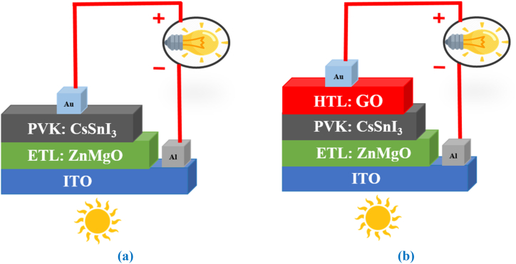
Firstly, over the ITO top electrode, a 0.1 μm thick ZnMgO material is used that serves as the ETL. The PSC design employs it to efficiently gather the electrons generated in the absorber layers. Whereas, for the collection of the holes, we implement GO of 0.1 μm as the HTL. Lastly, the absorber layer (CsSnI3) for the devices has a thickness level of 0.1 μm placed in between HTL and ETL (Fig. 1(a)-(b)). The study comprises the thickness variation from 0.25 μm to 2.0 μm shown in the results and discussion. The PVK-generated hole is gathered and transported to the cathode by the hooping mechanism. Au, having a thickness of 0.1 μm, serves as the cathode in the PSC. All the constituent parameters taken for the simulation are written in Table 1, Table 2.
Fig. 1.
Schematic architecture of CsSnI3-based PSC devices (a) without HTL (b) with HTL.
Table 1.
| Terms | Parameters | ITO | ETM (ZnMgO) | PVK (CsSnI3) | HTM (GO) |
|---|---|---|---|---|---|
| Thickness | d (μm) | 0.1 | 0.1 | 0.1* | 0.1 |
| Bandgaps | Eg(eV) | 3.6 | 3.33 | 1.27 | 2.48 |
| Relative Permittivity | εr | 10 | 9 | 10.59 | 10 |
| Elect. affinity | χ(eV) | 4.1 | 3.9 | 4.47 | 2.3 |
| Elec. thermal velocity (cm.s−1) | ve | 1 × 10⁷ | 1 × 10⁷ | 1 × 10⁷ | 5.2 × 10⁷ |
| Hole thermal velocity (cm.s−1) | Vh | 1 × 10⁷ | 1 × 10⁷ | 1 × 10⁷ | 5.0 × 10⁷ |
| Effective DoS at CB. | Nc(cm−3) | 2 × 10¹⁸ | 1 × 10²¹ | 1.58 × 10¹⁹ | 2.2 × 10¹⁸ |
| Effective DoS at VB. | Nv(cm−3) | 1.8 × 10¹⁹ | 2 × 10²⁰ | 1.47 × 10¹⁸ | 1.8 × 10¹⁹ |
| Mob. of electrons | μn(cm2/Vs) | 50 | 20 | 4.37 | 26 |
| Mob. of holes | μp(cm2/Vs) | 75 | 10 | 4.37 | 123 |
| Dop. conc. of acceptor | Na(cm−3) | 0 | 1 | 1 × 10¹⁵ | 1 × 10¹⁸ |
| Dop. conc. of donor | Nd(cm−3) | 1 × 10¹⁸ | 1 × 10¹⁹ | 0 | 0 |
| Def. Density | Nt(cm−3) | 1 × 10¹² | 1 × 10¹² | 1 × 10¹² | 1 × 10¹² |
Table 2.
Parameter of interface defects used in simulations.
| Parameters | GO/CsSnI3 and CsSnI3/ZnMgO |
|---|---|
| Type of defect | Neutral |
| Capture cross section of Electrons (cm2) | 1 × 10⁻¹⁹ |
| Capture cross section of Holes (cm2) | 1 × 10⁻¹⁹ |
| Energy distributions | single |
| Reference for def. energy level | Above the highest EV |
| Energy with respect to reference (eV) | 0.6 |
| Total density (cm−2) | 1 × 10⁹ |
3. Mathematical modeling
The Simulating software of SCAPS-1D was invented by Burgelman et al. which permits the numerical modelling of the key parameters influencing the PSC device output. Under steady-state circumstances, the semiconductor materials are governed by the one-dimensional equation. The p-n junction's electric fields (E) and the charge density relationship can be depicted using the following equation (Eq. 1) [26],
| (1) |
in this case, the electrostatic potential (), the charge (q), the static relative permittivity () of the medium, the electrons, and the hole (n and p), respectively; while the donor and acceptor density, and the acceptor and donor defect density ( and ).
While the continuity equation of the carrier in the device can be represented using the following equation (Eq. 2 and Eq. (3)):
| (2) |
| (3) |
where the electron/hole current density (), the carrier generation rate (), and electron/hole recombination / ), respectively.
At the same time, the current density of the carrier's are also shown in the equations (Eq. 4 and Eq. (5)) [27],
| (4) |
| (5) |
here, is the charge, and is the carrier mobilities and is the carrier's diffusion coefficient. It also needs to be mentioned that the solar cell's basic equation for current density, recombination, and generation rate, is extracted by the SCAPS-1D software.
4. Results and discussions
The full investigation and analysis of intrinsic solar cell characteristics are covered in the seven subsections that comprise the Results and discussion segment numbered 4.1 to 4.8.
4.1. Bandgap alignment of CsSnI3-based PSC device
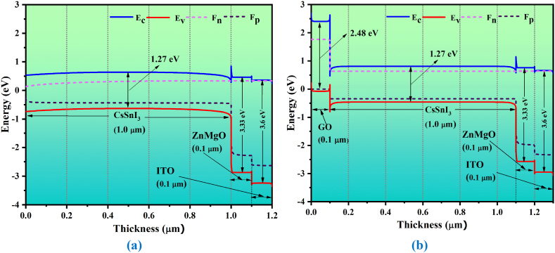
The band energy alignment controls the amount of heterojunction current flow. The optimized energy band diagram is displayed in Fig. 2(a) without HTL and 2(b) with HTL (GO). Based on the results of the SCAPS simulation's energy band panel data show the thickness of the layer and each material's bandgap. It can be observed that for the various doping concentration levels utilized in this investigation. It is simple to see from Fig. 2 the band bending that takes place between the GO and CsSnI3 layer. For CsSnI3-based PSC, the quick movement of electrons can be depicted. The potential for the suggested solar cell to deliver the specified performance is confirmed by this diagram. As the flow of the electron and hole can be well predicted for the band energy diagram for the designed PSC. The kink has appeared due to offset in the energy levels however the height of the kink is lower than the thermal energy therefore it would not cause any problem for the carrier transport.
Fig. 2.
The band energy diagrams for the CsSnI3-based PSC architecture (a) without HTL and (b) with HTL.
4.2. The impact of thickness in CsSnI3 layer and acceptor density
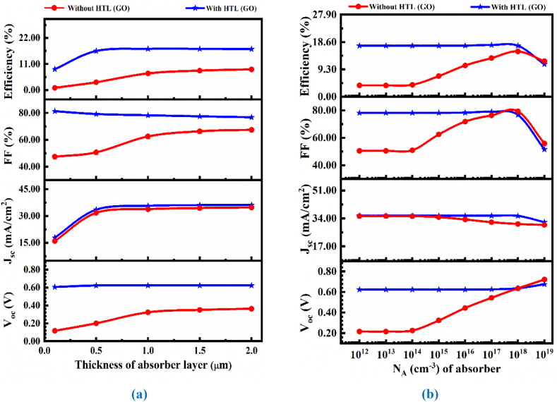
The input parameters of the constituent layer of the PSC are depicted in Table 1 at 300 K temperature, which is also utilized for the entire simulation analysis. The influence of the absorber thicknesses on the CsSnI3-based PSCs' output characteristics has been displayed in Fig. 3(a). As the perovskiteCsSnI3layer thickness grows for the devices, the JSC rises and achieves a saturated value of 35.60/cm2 at 1.0 μm. Then, the value of the JSC keeps increasing slightly on the further increasing thickness, which is attributed to the recombination kinetics that come into play over the charge separation in the proposed PSC device. Additionally, it is expected that the net absorption up to the CsSnI3 thickness of 1.0 μm becomes enhanced, which yields a higher production rate of exactions. This initiates a better generation of electrons in the absorber layer due to the wide absorption of photons. Simultaneously, the variation of VOC w.r.t the CsSnI3 thickness ranging from 0.1 μm to 2.0 μm is also shown. It shows a maximum at 0.5 μm thickness and then indicates a constant trend, which is clearly governed by recombination kinetics that dominates at high thickness [23].
Fig. 3.
(a) The influence of changing the CsSnI3 thickness without and with the HTL layer (b) The acceptor density influence in the CsSnI3 perovskite with and without the HTL layer.
While FF of the device exhibits an average proportional increase on the increment of the absorber thickness and is likely to achieve a saturation value around a thickness of 1.0 μm. It can be observed that the fluctuation of efficiency for PSCs across the thickness of the CsSnI3. Due to the direct impact of the thickness on the JSC, VOC, and FF, the efficiency of the PSC leads to a maximum thickness of around 1.0 μm. The advantage of the perovskite may result from photons being absorbed in broader frequencies due to a greater bandgap [28]. The Diffusion Length for the thickness level of 1.0 μm is: Ln = 3.4 × 101 μm, Lp = 3.4 × 101 μm, respectively.
NA is changed in the CsSnI3 from 1012 to 1019 cm−3 to examine its belongings on the overall efficiency of the suggested PSC architecture. The change in the NA influence in the absorber (CsSnI3) layer is shown in Fig. 3(b). The goal of increasing VOC from 0.62 to 0.67 V and decreasing JSC from 35.63 to 31.71 mA/cm2 was to change the NA value in the CsSnI3 material from 1012 to 1019. The FF remains constant until 1018, when it starts to decrease. When NA is more than 1018 cm−3, the surplus carrier induces recombination and increases scattering, which reduces cell efficiency.
4.3. The impact of ZnMgO and GO thickness and acceptor density on the PSC outputs
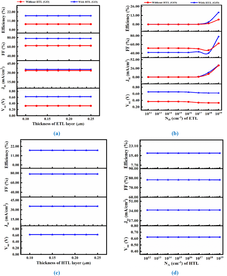
The input properties of the ZnMgO layer in the PSC are taken from Table 1 at 300 K temperature and is utilized for the entire simulation analysis. The effect of the ZnMgO ETL thicknesses on the CsSnI3-based PSC's output characteristics has been displayed in Fig. 4(a). As the ZnMgO thickness shows a lesser impact on the JSC and shows a value of ranges 35.6092 mA/cm2 - 35.6091 mA/cm2 at 0.1–0.2 μm, respectively. A similar trend can be observed for VOC [29]. It can be noted that the highest value of efficiency of 17.37 % is reached for 0.1 μm of the ZnMgO layer. A similar value can be seen for the GO thickness range in Fig. 4(c). The optimized thickness of 0.1 μm for the GO layer is obtained for the highest simulated efficiency of 17.37 %.
Fig. 4.
(a) The influence of variation in ZnMgO thickness with and without the HTL layer, (b) The acceptor density influence of ZnMgO with and without the HTL layer,(c) The influence of varying GO HTL layer thickness, (d) The acceptor density influence in the GO-HTL layer.
Since ND is changed in the ETL (ZnMgO) layer from 1012 to 1019 cm−3, examine its influence on the output of the suggested PSC device illustrated in Fig. 4(b). The FF remains constant until 1017, at which point it starts to decrease until 1018. The cell efficiency remains constant until 1017, at which point it increases. In Fig. 4(d) HTL (GO) shallow uniform acceptor density shows a lesser impact on the JSC, VOC, FF, and efficiency.
4.4. The temperature influence on the PSC outputs
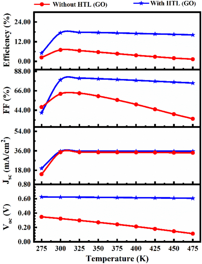
The complete analysis of PSC properties with temperature fluctuation is depicted in Fig. 5. While temperatures rise from 275 K to 475 K, the PV characteristics of CsSnI3-based solar cells with and without a back surface field are expressively decreased. The VOC depends on the splitting of the Fermi level and during temperature variation the splitting of the Fermi level was insignificant therefore VOC remained constant for HTL-based devices. As the PCE for the ITO/ZnMgO/CsSnI3/GO and ITO/ZnMgO/CsSnI3 structures is found to be 17.37 % and 7.03 %, respectively, at 300 K, but it decreases to 16.15 % and 1.34 %, correspondingly, owing to the increase in the simulating temperature to 475 K. CsSnI3-based PSC with a back surface field (BSF) exhibits better thermal stability than without BSF, according to these simulation results.
Fig. 5.
The influence of temperature on solar cell outputs at optimizing conditions.
High temperatures and fixed irradiance yield extensively higher electron-hole pairs while maintaining the identical JSC value. The band gap of CsSnI3 narrows as the working temperature increases, and the reverse saturation current intensifies, lowering the VOC, FF, and efficiency. The bandgap energy of a photovoltaic solar cell decreases with an increase in its operating temperature, which causes a slight rise in JSC and reduces VOC. As a result, the decrease in VOC and the negligible increase in JSC cause the FF and PCE of the solar cells to decrease at higher temperatures [30].
4.5. Collective impact of the total defect - density and thickness on the PSC
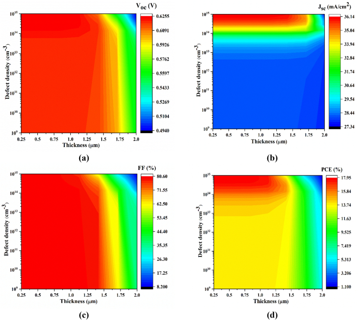
The contour analysis with the combined influence of the defect density and thickness on performance parameters under the optimized conditions has been discussed. The plotting explicitly helps in understanding the defect concentrations at various absorber layers (i.e., CsSnI3) thickness helps us to comprehend how the device performs when the variations of defect and thickness are combined [31].
This section is thus devoted to investigating the collective variation to understand the device characteristics more precisely. The defect density is increased from 109 to 1015 cm−3, while the thickness of the absorber layers varies from 0.25 μm to 2.0 μm to show the combined influence on PSC performance. The influence of the CsSnI3-based PSC device on thickness and defect density is depicted in Fig. 6(a-d). The perovskite absorber layer of CsSnI3, with a thickness of 1.5 μm and a defect density of 109 cm−3, exhibits the highest JSC of 36.14 mA/cm2. In contrast, a region with a lower thickness and high defect density value shows the minimum value of JSC. In the CsSnI3-based PSC, the VOC also indicates a smaller impact, the smallest due to the recombination profile [32]. The FF is nearly the same and achieves a high value of 80.60 % in low-density and lower-thickness regions. Thus, an optimal absorber thickness of 1.0 μm may result in a high VOC of the order of 0.623 V. The ideal value of PCE is 17.37 %, and it has been established using a constant thickness of 1.0 μm for the CsSnI3 absorber layer and the defect concentration of 1012 cm−3.
Fig. 6.
Combined influence of CsSnI3 thickness and total defect density on solar cell characteristics. (a) VOC(b) JSC(c) FF and (d) PCE.
4.6. The capacitance-voltage (C–V) influence on the PSC
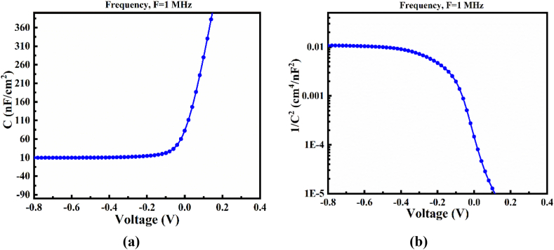
The capacitance-voltage (C–V) study was conducted for the frequency of 1 MHz to verify the consistency of the analysis. The p-n junctions are coupled to the depletion and diffusion capacitances. At forward bias voltage, diffusion capacitance dominates, whereas, at reverse bias voltage, depletion capacitance is higher in size. The capacitance at zero bias voltage of a p-n junction PSC is 10 nF-cm−2, as shown in Fig. 7(a). The capacitance increases rapidly as the polarization potential's voltage and frequency increase. Effective trapping does not diminish the effective charge at the reverse bias, which increases capacitance [33]. The Mott-Schottky plot of the PV cell is shown in Fig. 7(b). The potential of the flat band for the suggested solar cell is obtained by intersecting the 1/C2 plot with the x-axis representing voltage. The decreasing slope of the graph suggests that holes mainly populate the p-type CsSnI3 layer and the space charge region. Exposure of the CsSnI3 layer to sunlight may result in a high carrier density, potentially due to photo-generated carriers. The slight variation in 1/C2 might be due to localized deep states within the absorber layer. The primary influence results from the adjustment of the dominant carriers, not from the influence of the deep states.
Fig. 7.
At Frequency = 1 MHz, (a) influence of C–V on solar cell (b) 1/C2–V curve.
4.7. The impact of resistances on the outputs of the PSC
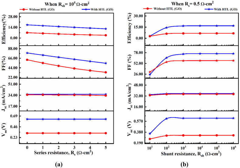
The influence of series-shunt (Rs-Rsh) resistances for the suggested PSC structure with and without BSF are depicted in Fig. 8. Parasitic resistances such as Rs and Rsh have an impact on the outputs of all PV systems. In addition to the rear and front metallic resistances, the bulk resistance also contributes to the structure's series of resistances. A manufacturing error produced the shunt (Rsh) resistances through a separate carrier recombination path. Besides, the shunt (Rsh) resistances were produced by a manufacturing error through a separate carrier recombination path. Naturally, the upgraded, highly efficient solar cell has a lower Rs and a higher Rsh, which affects the cell structure. Here, Rs was changed from 0 to 5 Ω-cm2, and the shunt resistance, Rsh, was fixed at 105 Ω-cm2. The JSC and VOC are almost unaffected by changes in Rs, as seen in Fig. 8(a). Yet, it is perceived that the increasing value of Rs significantly affects the FF and PCE. Thus, the change in Rs, the FF is reduced from 77.21 to 54.48 %, and the PCE from 17.37 to 13.06 %. (0–5 Ω-cm2). Finally, it is demonstrated that cell structures with smaller Rs are more effective, which is in good agreement with the reputable report [34]. The series resistance Rs has been adjusted from 101 to 106 Ω-cm2 while Rsh remains constant at 0.5 Ω-cm2. The proposed solar cell's entire PV parameter is initially enhanced and eventually tends toward saturation, as depicted in Fig. 8(b). We can obtain that the overall efficiency of the proposed PSC having the GO layer (HTL) improved from 2.91 % to 17.37 % concerning the rise in Rsh, which better agrees with the existing literature [35].
Fig. 8.
The influence of the change of (a) Rs and (b) Rsh with and without HTL.
4.8. J-V parameters of designed PSC devices
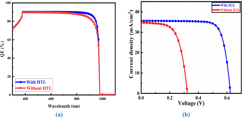
Fig. 9(a-b) shows the QE as well as the J-V parameter for the CsSnI3-based PSC device with and without HTL (GO) layer after optimizing influenced parameters such as PAL and CTL thickness, defectivity, temperature, interface defectivity, and resistances. The optimized value of QE can be obtained for the with HTL condition. The optimized value is due to the addition of the HTL; i.e. GO. As the GO can absorb some fraction of the photons. Due to the absorption, the 5 % increment in QE can be seen. For comparison, with HTL condition offers around 90 % QE value as depicted below. On the contrary, it can be obtained that the J value decreases at 0.21 V and drops at 0.33 V in the without HTL (GO) PSC device. The optimum JSC value of 34.76 mA/cm2 is reached in this condition. On the contrary, the J starts to decrease at 0.5 V and drops at 0.62 V in with HTL (GO) PSC device with JSC value optimized to 35.60 mA/cm2. The highest value of JSC is due to a lesser bandgap, i.e., 1.3 eV of the absorber material. On the contrary, the detailed comparison with different combinations of ETL and HTL is shown in Table 3. At last, the CsSnI3-based PSC offers higher results than the earlier existing literature, as shown in Table 4.
Fig. 9.
(a) The QE and (b) J-V parameters for CsSnI3-based PSC at all optimized conditions.
Table 3.
The detailed analysis of simulated PSCs with different ETL and HTL combinations.
| Device architecture | JSC (mA/cm2) | VOC (V) | FF (%) | PCE (%) |
|---|---|---|---|---|
| ZnMgO/CsSnI3/GO-based PSC | 35.609 | 0.6236 | 78.21 | 17.37 |
| TiO2/CsSnI3/GO-based PSC | 35.604 | 0.6204 | 78.18 | 17.04 |
| ZnO/CsSnI3/GO-based PSC | 35.605 | 0.6201 | 78.11 | 17.24 |
| ZnMgO/CsSnI3/Spiro-OMeTAD | 35.515 | 0.6135 | 78.02 | 16.99 |
| TiO2/CsSnI3/Spiro-OMeTAD | 35.482 | 0.6024 | 77.89 | 16.64 |
| ZnO/CsSnI3/Spiro-OMeTAD | 35.480 | 0.6018 | 77.78 | 16.60 |
Table 4.
Simulated PV device characteristics along with earlier works.
| S/N | Field of research | PVK | HTL | Efficiency (%) | References |
|---|---|---|---|---|---|
| 1 | Experimental | CsSnI3 | Without HTL | 3 | [36] |
| 2 | Experimental | CsSnI3 | Without HTL | 7.5 | [37] |
| 3 | Theoretical | CsSnI3 | Without HTL | 13.42 | [38] |
| 4 | Theoretical | CsSnI3 | With HTL (PCBM) | 11 | [26] |
| 5 | Theoretical | CsSnI3 | Without HTL | 7.03* | This work |
| 6 | Theoretical | CsSnI3 | With HTL (GO) | 17.37* | This work |
Note: [*] indicates proposed the cell.
Initially, Au is used in the simulation of the PSC device. We replace Au with some of the back electrodes, such as Cu, Ag, Fe, C, and Au; as shown in Table 5. It can be observed that the performance of the cell is best for the Au. So, the entire simulation was accomplished considering the Au as the suitable back contact. It can be well explained that while increasing the work function, the height of the barrier of the majority carrier decreases, which ultimately results in an increased ohmic contact. So, while increasing the metal work functions, the overall open circuit voltage (VOC) and efficiency (PCE) also increased.
Table 5.
The operational work function of the back metal contacts.
| Back metal contact | Cu | Ag | Fe | C | Au |
|---|---|---|---|---|---|
| Work function (eV) | 4.65 | 4.26 | 4.81 | 5 | 5.1 |
5. Conclusions
Design and simulation studies on the PSC structures ITO/ZnMgO/CsSnI3/GO/Au configuration have been utilized using SCAPS-1D simulating software. The ZnMgO has been used as ETL, keeping in view of minimizing the cost of environment-friendly solar devices, whereas, for the collection of the holes, novel GO is the HTL for the extensive simulation of the PSC device. CsSnI3 is an active absorber layer, exhibiting a more considerable influence on the optoelectrical parameter as compared to the PSC device's CTLs. So, the optimization of absorber thicknesses for the PSC is carried out for better outputs. In the present study, we determined that the CsSnI3-based PSC device has an optimized CsSnI3 thickness of 1.0 μm. Also, the defectivity of the PSC shows that at the level of 1012 cm−3, it obtains higher outputs. Moreover, the study also includes the impact of the resistances for enhancing the higher efficiency of the PSC device. The simulation clearly exhibits that the ZnMgO with GO used as CTL can provide excellent outputs, as in the present case, nearly 17.37 %, which may be a fascinating and suitable option in the development of the PSC. Therefore, the overall conclusion of the present study may offer a valuable contribution regarding the manufacturing of more efficient CsSnI3-based PSC devices.
Funding
This work was funded by the Researchers Supporting Project Number (RSP2023R267) King Saud University, Riyadh, Saudi Arabia.
Data availability
Data will be made available on request.
CRediT authorship contribution statement
Sagar Bhattarai: Writing - review & editing, Writing - original draft, Methodology, Investigation, Formal analysis, Data curation, Conceptualization. M. Khalid Hossain: Writing - review & editing, Project administration, Methodology, Investigation, Funding acquisition, Formal analysis, Data curation, Conceptualization. Rahul Pandey: Writing - review & editing, Visualization, Validation. Jaya Madan: Writing - review & editing, Visualization, Validation, Conceptualization. D.P. Samajdar: Writing - review & editing, Visualization, Validation. Mithun Chowdhury: Writing - review & editing, Visualization, Validation. Md. Ferdous Rahman: Writing - review & editing, Visualization, Validation. Mohd Zahid Ansari: Writing - review & editing, Visualization, Validation, Conceptualization. Munirah D. Albaqami: Writing - review & editing.
Declaration of competing interest
The authors declare that they have no known competing financial interests or personal relationships that could have appeared to influence the work reported in this paper.
Acknowledgements
This work was funded by the Researchers Supporting Project Number (RSP2023R267) King Saud University, Riyadh, Saudi Arabia. The SCAPS-1D program was kindly provided by Dr. M. Burgelman of the University of Gent in Belgium. The authors would like to express their gratitude to him.
Contributor Information
Sagar Bhattarai, Email: sagarbhattarai012@gmail.com.
M. Khalid Hossain, Email: khalid.baec@gmail.com, khalid@kyudai.jp.
Rahul Pandey, Email: rahul.pandey@chitkara.edu.in.
Jaya Madan, Email: jaya.madan@chitkara.edu.in.
Mohd Zahid Ansari, Email: zahid.smr@yu.ac.kr.
References
- 1.Thakur A., Singh D., Kaur Gill S. Numerical simulations of 26.11% efficient planar CH3NH3PbI3 perovskite n-i-p solar cell. Mater. Today Proc. 2022;71:195–201. doi: 10.1016/j.matpr.2022.08.423. [DOI] [Google Scholar]
- 2.Dureja T., Garg A., Bhalla S., Bhutani D., Khanna A. Double lead-free perovskite solar cell for 19.9% conversion efficiency: a SCAPS-1D based simulation study. Mater. Today Proc. 2022;71:239–242. doi: 10.1016/j.matpr.2022.08.518. [DOI] [Google Scholar]
- 3.Karthick S., Velumani S., Bouclé J. Experimental and SCAPS simulated formamidinium perovskite solar cells: a comparison of device performance. Sol. Energy. 2020;205:349–357. doi: 10.1016/j.solener.2020.05.041. [DOI] [Google Scholar]
- 4.Kojima A., Teshima K., Shirai Y., Miyasaka T. Organometal halide perovskites as Visible-light sensitizers for photovoltaic cells. J. Am. Chem. Soc. 2009;131:6050–6051. doi: 10.1021/ja809598r. [DOI] [PubMed] [Google Scholar]
- 5.Raoui Y., Ez-Zahraouy H., Tahiri N., El Bounagui O., Ahmad S., Kazim S. Performance analysis of MAPbI3 based perovskite solar cells employing diverse charge selective contacts: simulation study. Sol. Energy. 2019;193:948–955. doi: 10.1016/j.solener.2019.10.009. [DOI] [Google Scholar]
- 6.Im J.-H., Lee C.-R., Lee J.-W., Park S.-W., Park N.-G. 6.5% efficient perovskite quantum-dot-sensitized solar cell. Nanoscale. 2011;3:4088. doi: 10.1039/c1nr10867k. [DOI] [PubMed] [Google Scholar]
- 7.Gupta G., Verma S., Nagarajan R., Rath S. Microstructural and bandgap investigations of wurtzite-phase ZnMgO nanopowders synthesized by ball-milling. Phys. B Condens. Matter. 2021;604 doi: 10.1016/j.physb.2020.412735. [DOI] [Google Scholar]
- 8.Bhattarai S., Pandey R., Madan J., Mhamdi A., Bouazizi A., Muchahary D., Gogoi D., Sharma A., Das T.D. Investigation of carrier transport materials for performance assessment of lead-free perovskite solar cells. IEEE Trans. Electron. Dev. 2022;69:3217–3224. doi: 10.1109/TED.2022.3165516. [DOI] [Google Scholar]
- 9.Kim H.-S., Im S.H., Park N.-G. Organolead halide perovskite: new horizons in solar cell research. J. Phys. Chem. C. 2014;118:5615–5625. doi: 10.1021/jp409025w. [DOI] [Google Scholar]
- 10.Liu M., Johnston M.B., Snaith H.J. Efficient planar heterojunction perovskite solar cells by vapour deposition. Nature. 2013;501:395–398. doi: 10.1038/nature12509. [DOI] [PubMed] [Google Scholar]
- 11.Pandey R., Khanna A., Singh K., Patel S.K., Singh H., Madan J. Device simulations: toward the design of >13% efficient PbS colloidal quantum dot solar cell. Sol. Energy. 2020;207:893–902. doi: 10.1016/j.solener.2020.06.099. [DOI] [Google Scholar]
- 12.Wu B., Zhou Y., Xing G., Xu Q., Garces H.F., Solanki A., Goh T.W., Padture N.P., Sum T.C. Long minority‐carrier diffusion Length and low surface‐recombination velocity in inorganic lead‐free CsSnI 3 perovskite crystal for solar cells. Adv. Funct. Mater. 2017;27 doi: 10.1002/adfm.201604818. [DOI] [Google Scholar]
- 13.Chen L.-J., Lee C.-R., Chuang Y.-J., Wu Z.-H., Chen C. Synthesis and optical properties of lead-free cesium tin halide perovskite quantum rods with high-performance solar cell application. J. Phys. Chem. Lett. 2016;7:5028–5035. doi: 10.1021/acs.jpclett.6b02344. [DOI] [PubMed] [Google Scholar]
- 14.Shum K., Chen Z., Qureshi J., Yu C., Wang J.J., Pfenninger W., Vockic N., Midgley J., Kenney J.T. Synthesis and characterization of CsSnI3 thin films. Appl. Phys. Lett. 2010;96 doi: 10.1063/1.3442511. [DOI] [Google Scholar]
- 15.Chen Z., Yu C., Shum K., Wang J.J., Pfenninger W., Vockic N., Midgley J., Kenney J.T. Photoluminescence study of polycrystalline CsSnI3 thin films: determination of exciton binding energy. J. Lumin. 2012;132:345–349. doi: 10.1016/j.jlumin.2011.09.006. [DOI] [Google Scholar]
- 16.Arbouz H. Optimization of lead-free CsSnI3-based perovskite solar cell structure. Appl. Rheol. 2023;33:1–6. doi: 10.1515/arh-2022-0138. [DOI] [Google Scholar]
- 17.Lin S., Zhang B., Lü T.-Y., Zheng J.-C., Pan H., Chen H., Lin C., Li X., Zhou J. Inorganic lead-free B-γ-CsSnI 3 perovskite solar cells using diverse electron-transporting materials: a simulation study. ACS Omega. 2021;6:26689–26698. doi: 10.1021/acsomega.1c04096. [DOI] [PMC free article] [PubMed] [Google Scholar]
- 18.Bin Song T.-B., Yokoyama T., Logsdon J., Wasielewski M.R., Aramaki S., Kanatzidis M.G. Piperazine suppresses self-doping in CsSnI 3 perovskite solar cells. ACS Appl. Energy Mater. 2018;1:4221–4226. doi: 10.1021/acsaem.8b00866. [DOI] [Google Scholar]
- 19.Wei J., Xiong Q., Mahpeykar S.M., Wang X. Numerical study of complementary nanostructures for light trapping in colloidal quantum dot solar cells. Nanomaterials. 2016;6 doi: 10.3390/nano6040055. [DOI] [PMC free article] [PubMed] [Google Scholar]
- 20.Bhattarai S., Pandey R., Madan J., Ahmed F., Shabnam S. Performance improvement approach of all inorganic perovskite solar cell with numerical simulation. Mater. Today Commun. 2022;33 doi: 10.1016/j.mtcomm.2022.104364. [DOI] [Google Scholar]
- 21.Burgelman M., Verschraegen J., Degrave S., Nollet P. Modeling thin-film PV devices. Prog. Photovoltaics Res. Appl. 2004;12:143–153. doi: 10.1002/pip.524. [DOI] [Google Scholar]
- 22.Decock K., Lauwaert J., Burgelman M. Characterization of graded CIGS solar cells. Energy Proc. 2010;2:49–54. doi: 10.1016/j.egypro.2010.07.009. [DOI] [Google Scholar]
- 23.Hossain M.K., Samajdar D.P., Das R.C., Arnab A.A., Rahman M.F., Rubel M.H.K., Islam M.R., Bencherif H., Pandey R., Madan J., Mohammed M.K.A. Design and simulation of Cs 2 BiAgI 6 double perovskite solar cells with different electron transport layers for efficiency enhancement. Energy Fuels. 2023;37:3957–3979. doi: 10.1021/acs.energyfuels.3c00181. [DOI] [Google Scholar]
- 24.Safa Sultana R., Bahar A.N., Asaduzzaman M., Ahmed K. Numerical modeling of a CdS/CdTe photovoltaic cell based on ZnTe BSF layer with optimum thickness of absorber layer. Cogent Eng. 2017;4 doi: 10.1080/23311916.2017.1318459. [DOI] [Google Scholar]
- 25.Widianto E., Shobih, Rosa E.S., Triyana K., Nursam N.M., Santoso I. Performance analysis of carbon-based perovskite solar cells by graphene oxide as hole transport layer: experimental and numerical simulation. Opt. Mater. 2021;121 doi: 10.1016/j.optmat.2021.111584. [DOI] [Google Scholar]
- 26.Rahman M.S., Miah S., Marma M.S.W., Ibrahim M. 2020 IEEE Reg. 10 Conf. IEEE; 2020. Numerical simulation of CsSnI 3 -based perovskite solar cells: influence of doped-ITO front contact; pp. 140–145. [DOI] [Google Scholar]
- 27.Rai S., Pandey B.K., Dwivedi D.K. Modeling of highly efficient and low cost CH3NH3Pb(I1-xClx)3 based perovskite solar cell by numerical simulation. Opt. Mater. 2020;100 doi: 10.1016/j.optmat.2019.109631. [DOI] [Google Scholar]
- 28.Hossain M.K., Toki G.F.I., Kuddus A., Rubel M.H.K., Hossain M.M., Bencherif H., Rahman M.F., Islam M.R., Mushtaq M. An extensive study on multiple ETL and HTL layers to design and simulation of high-performance lead-free CsSnCl3-based perovskite solar cells. Sci. Rep. 2023;13:2521. doi: 10.1038/s41598-023-28506-2. [DOI] [PMC free article] [PubMed] [Google Scholar]
- 29.Benabbas S., Heriche H., Rouabah Z., Chelali N. 2014 North African Work. Dielectic Mater. Photovolt. Syst. IEEE; 2014. Enhancing the efficiency of CIGS thin film solar cells by inserting novel back surface field (SnS) layer; pp. 1–5. [DOI] [Google Scholar]
- 30.Abdalmageed H.I., Fedawy M., Aly M.H. Effect of absorber layer bandgap of CIGS-based solar cell with (CdS/ZnS) buffer layer. J. Phys. Conf. Ser. 2021;2128 doi: 10.1088/1742-6596/2128/1/012009. [DOI] [Google Scholar]
- 31.Taheri S., Ahmadkhan kordbacheh A., Minbashi M., Hajjiah A. Effect of defects on high efficient perovskite solar cells. Opt. Mater. 2021;111 doi: 10.1016/j.optmat.2020.110601. [DOI] [Google Scholar]
- 32.Hossain M.K., Bhattarai S., Arnab A.A., Mohammed M.K.A., Pandey R., Ali M.H., Rahman M.F., Islam M.R., Samajdar D.P., Madan J., Bencherif H., Dwivedi D.K., Amami M. Harnessing the potential of CsPbBr3-based perovskite solar cells using efficient charge transport materials and global optimization. RSC Adv. 2023;13:21044–21062. doi: 10.1039/D3RA02485G. [DOI] [PMC free article] [PubMed] [Google Scholar]
- 33.Gupta G.K., Garg A., Dixit A. Electrical and impedance spectroscopy analysis of sol-gel derived spin coated Cu 2 ZnSnS 4 solar cell. J. Appl. Phys. 2018;123 doi: 10.1063/1.5002619. [DOI] [Google Scholar]
- 34.Rahman M.A. Numerical modeling of ultra-thin CuSbS 2 heterojunction solar cell with TiO 2 electron transport and CuAlO 2 :Mg BSF layers. Opt. Mater. Express. 2022;12:2954. doi: 10.1364/ome.465498. [DOI] [Google Scholar]
- 35.Hosen A., Mian M.S., Al Ahmed S.R. Improving the performance of lead‐free FASnI 3 ‐based perovskite solar cell with Nb 2 O 5 as an electron transport layer. Adv. Theory Simulations. 2023;6 doi: 10.1002/adts.202200652. [DOI] [Google Scholar]
- 36.Zhang T., Li H., Ban H., Sun Q., Shen Y., Wang M. Efficient CsSnI 3 -based inorganic perovskite solar cells based on a mesoscopic metal oxide framework via incorporating a donor element. J. Mater. Chem. A. 2020;8:4118–4124. doi: 10.1039/C9TA11794F. [DOI] [Google Scholar]
- 37.Ye T., Wang K.K., Hou Y., Yang D., Smith N., Magill B., Yoon J., Mudiyanselage R.R.H.H., Khodaparast G.A., Wang K.K., Priya S. Ambient-air-stable lead-free CsSnI 3 solar cells with greater than 7.5% efficiency. J. Am. Chem. Soc. 2021;143:4319–4328. doi: 10.1021/jacs.0c13069. [DOI] [PubMed] [Google Scholar]
- 38.Xu X., Wang J., Cao D., Zhou Y., Jiao Z. Design of all-inorganic hole-transport-material-free CsPbI 3/CsSnI 3 heterojunction solar cells by device simulation. Mater. Res. Express. 2022;9 doi: 10.1088/2053-1591/ac5778. [DOI] [Google Scholar]
Associated Data
This section collects any data citations, data availability statements, or supplementary materials included in this article.
Data Availability Statement
Data will be made available on request.


