

Abstract

An unexplored material of copper boride has been realized recently in two-dimensional form at a (111) surface of the fcc copper crystal. Here, one-dimensional (1-D) boron growth was observed on the Cu(110) surface, as probed by atomically resolved scanning probe microscopy. The 1-D copper boride was composed of quasi-periodic atomic chains periodically aligned parallel to each other, as confirmed by Fourier transform analysis. The 1-D growth unexpectedly proceeded across surface steps in a self-assembled manner and extended over several 100 nm. The long-range formation of a 1-D quasi-periodic structure on a surface has been theoretically modeled as a 1-D quasi-crystal and the predicted conditions matched the structural parameters obtained by the experimental work here. The quasi-periodic 1-D copper boride system enabled a way to examine 1-D quasi-crystallinity on an actual material.
Keywords: boron, Cu(110), one dimension, quasi-periodicity, boride
A crystal surface is sandwiched between a vacuum and a substrate, where the atoms are restrained in a two-dimensional (2-D) lattice and can diffuse to and from the bulk. Surface layers have been reported to grow on substrates commensurately or incommensurately, depending on a balance between adsorbate–adsorbate and adsorbate–substrate interactions. The degree of freedom, being specific to a surface, results in the formation of exotic long-range ordered phases such as superstructures and Moiré patterns. This unique environment has opened new research fields and has provided a space to examine interface materials that cannot be explored in a pure 2-D system.1−4 One of the recent findings was a long-range ordered layer of copper boride (Cu-Boride) that was grown incommensurately on the (111) surface of a copper crystal.5−7 This was unexpected because boron has been known to rarely form bulk compounds with group 11 elements.8,9 Moreover, the 2-D copper boride was composed of an alternating array of boron and copper chains, which indicated an intriguing relationship between the 2-D and 1-D atomic structures. An appropriate choice of a 1-D template, such as the Cu (110) surface of the fcc crystal, has enabled us to grow atomic chains.10,11 Thus, a formation of the copper boride interface on Cu(110) is expected to lead to a unique 1-D system that can be characterized with surface-sensitive imaging, such as scanning tunneling microscopy (STM).
Here, we report the observation of a 1-D atomic structure of Cu-boron, prepared by depositing boron on Cu(110). The surface was composed of two types of unit lengths, one commensurate and the other incommensurate, with respect to the substrate lattice. A Fourier transform spectrum shows apparent signals that corresponded to delta-function peaks of quasi-periodicity. Hence, we designated the B/Cu(110) surface as an array of quasi-periodic chains. The domain grew anisotropically over surface steps, the direction of which was in contrast to conventional film growth on Cu(110), and it extended over several 100 nm in a self-assembled manner. Such a long-range 1-D quasi-periodic surface structure has been modeled as a 1-D quasi-crystal, and the structural parameters, obtained experimentally, satisfied formation conditions predicted by the theory. This system thus provides an actual interface material to examine 1-D quasi-crystals.
The initial boron growth on Cu(110) was imaged with STM, as shown in Figure 1a–d. There was a prominent domain with a taenioid shape that was separated from the clean Cu(110) region by clear domain boundaries. The adsorbate domain grew along the [11̅0] axis toward the steps, and as shown in Figure 1c,d, it even grew over the atomic steps, extending to the lower terraces in a self-assembled manner. The line-profile analysis across the B/Cu(110) domain, given in Figure 1e,f, unveils that the region appears 0.16–0.17 Å lower or higher than the clean Cu(110) area, depending on the sample bias. The height is much smaller than an atomic step of 1.2 Å, indicating that these areas are formed on the same surface terrace. After an extension of the adsorbate domain over the lower terrace, the domain-edge has a cliff-like structure with double step height when it reaches the edge. The growth mode was sharply in contrast to those commonly known on Cu(110) that retain the 1-D template structure and induce 1-D growth along surface steps.12,13 The extraordinary 1-D growth mode is seemingly related to the local atomic structures. Thus, it requires high-resolution image analyses before we discuss the growth mechanism. Figure 1g shows a magnified image of 1-D structures growing along the [11̅0] axis, separated by trenches. The 1.1 nm trench interval corresponded to 3a[001], where a[001] is the size of the Cu(110) unit cell along the [001] axis. This was the origin of the 3-fold periodicity that was also observed with electron diffraction.14,15 However, the 1-D structure in the [11̅0] direction was composed of bright and dark regions that could not be explained with regular translational symmetry. The contrast between self-assembled one-dimensional growth and the moderately disordered structure posed an intriguing situation of this novel Cu-Boride.14 To unveil the surface structural features, a process of the fast Fourier transform (FFT) was applied to Figure 1g to further examine the order of the 1-D system.
Figure 1.

Scanning tunneling microscopy (STM) images of the 1-D structure grown by boron deposition on Cu(110). (a, c) STM topography of the B/Cu(110) growth. The crystal orientations of the Cu substrate and scale bars are represented in white. Boundaries of the clean Cu(110) surface are indicated by black arrows. (b, d) Images of (a, c) after the graphically shading treatment16 to emphasize the boundaries. (e, f) The line profile taken from the white line of (a) and (c), respectively. (g) High-resolution STM image of the 1-D structure. (h) The two-dimensional power spectrum obtained by fast Fourier transform (FFT) of (g), with line profiles crossing the origin in [001] and [11̅0] direction. Image sizes and scanning parameters are (a) 123 × 123 nm2, It = 100 pA, Vs = 1.5 V. (c) 98 × 98 nm2, It = 103 pA, Vs = −0.01 mV, (g) 20 × 20 nm2, It = 100 pA, Vs = 1.5 V.
Figure 1h shows the 2-D power spectrum obtained via 2-D FFT (see details in the Supporting Information). Line profiles crossing the origin are shown in the figure. Spots along the [001] axis appeared periodically, which matched with the STM images of the 3-fold periodicity or the 3a[001] period (Figure 1g). A regular periodicity was not observed along the [11̅0] direction in the STM image, yet discrete spots corresponding to delta function peaks were observed in the FFT, as shown in Figure 1g. These Fourier spectra indicate a hidden periodicity in the 1-D structure. From the line profile, the spots could not be described by a periodic function with just a single unit vector, as in the case of 1-D crystals. Instead, the peak positions could all be explained via a linear combination of two basic units a and b with rational coefficients. The wavenumbers of individual peaks, given by a = 8.5 nm–1 and b = 11.6 nm–1 in reciprocal space, did not correspond to each other as reliable rational numbers, thus demonstrating the independence of the vectors. In general, structures other than random structures generate sets of finite vectors that can be explained by the linear combination of a basis set of reciprocal vectors. The number of the reciprocal vectors is called rank.17 In the regular crystal, the number of ranks is equal to the number of dimensions of the structure due to its translational symmetry. When the rank is higher than the dimension of the structure, the structure are called quasi-periodic.17,18 The existence of two vectors that could not be represented by each other verified the quasi-periodicity of the 1-D system here. The result explains the hidden periodicity, a quasi-periodicity, of the Cu-Boride chains. A similar spectrum was confirmed via 1-D FFT of the line scan in the STM image.15 Laue function analysis verified the appearance of reciprocal peaks in the nonuniform 1-D system.15
Both unit vectors a and b in reciprocal space corresponded to length 7.4 and 5.4 Å in real space, which were labeled as l1 and l2, respectively. To find the origins of these unique lengths along the chain, Figure 2a shows a typical STM image of the 1-D structure and the corresponding line profile. The STM apparent height can be categorized in the three zones: bottoms of the valleys (zone I), the intermediate (zone II), and the bright region (zone III). Lengths of the bright regions are described by an integer multiple of l2 and the peak protrusions follow the periodicity except for the defect sites indicated by inverted triangles in the figure. In the image, different types of the dark regions can be observed. The dominant type is the one with a length of 2l1 that is associated with a valley in zone III and the two shoulder features in zone II. The other type has the length, l2 + l1, and a faint protrusion can be found in zone II. Eventually, all region lengths can be scaled by summations of the two unit lengths with marginal uncertainties at the boundaries, and the quasi-periodic structure is composed of these two unit lengths. In addition, the length l1 matched fairly well with the commensurate 3a[11̅0] lattice, where a[11̅0] is the size of the Cu(110) unit cell, lp = 2.55 Å, along the [11̅0] axis. In contrast, l2 was indivisible by lp, and thus, it was incommensurate with the substrate lattice.
Figure 2.

Scanning tunneling microscopy (STM) analysis of the one-dimensional (1-D) structure of B/Cu(110) with the schematic image of the Aubry model. (a) Intensity line profile taken from white-dotted rectangle area of a single row of the STM image in Figure 1g, measured with unit length l1 and l2 for comparison. Length l1 and l2 correspond to red and green lines, respectively, and guidelines are presented each. The STM image is divided into three distinct zones I, II, and III based on their apparent height. Features such as shoulders and peaks within zone II and dips originating from defect sites within zone I are indicated by circles and inverted triangles, respectively. (b) Schematic image of definitions for the model to describe the 1-D quasi-periodic structure. For simplicity, the external potential was assumed to be sinusoidal with a period of lp(2π). Δ corresponds to a region where l2 adatoms are prohibited. Filled circles represents adatoms in regions of the l2 unit, and open circles are vacancies of the adatoms.
The distinctive features of the quasi-periodic 1-D structure in real space, characterized by its growth with two unit lengths, one of which was incommensurate with the substrate lattice, laid the groundwork for a deeper examination of the underlying mechanism. It has been known theoretically that a 1-D atomic chain can only exist via suppression of the structural fluctuations that increase with length (i.e., the number of chain atoms).19−21 Imposing periodic boundary conditions serves as a conventional approach to suppressing this divergence. For a quasi-periodic system on the external periodic structure, such as a quasi-periodic overlayer on a mismatched crystal surface, a suppression condition was developed by Aubry et al. based on an incommensurate modulation of the vacancy density of a periodic lattice20,21 and was extensively investigated.22
The 1-D quasi-periodic structure on a surface observed in the present
research is closely related to the theoretical model by Aubry et al.20−22 The authors made the condition for realizing such a system and discussed
that meeting the conditions can provide evidence for one-dimensional
quasi-crystals. Recalling the model, an incommensurate adatom chain
on a 1-D crystal lattice is considered. The chain contains the adatom
vacancies or adatom-free sites that coincide with the region (△)
within the substrate period where positioning of the adatom is prohibited.
Then, a condition of the chain formation was developed based on the
mean adatom density that corresponds to inverse of the mean adatom
distance. By incorporating the Aubry model, we hereby consider the
condition for formation of the 1-D structure at the B/Cu(110) surface15 as shown in Figure 2b. In the present system, as shown in Figure 2a, the bright region
in STM can be regarded as locations of the (boron) adatoms that were
characterized by the length, l2, while
the dark one was regarded as the adatom-free sites that was described
by l1. In the Aubry model, two characteristic
lengths were chosen to derive the mean length and the mean density.
Thus, it is fairly reasonable to choose the lengths l1 and l2 to derive the mean
length between the adatoms as lmean =
(1 – c)l2 + c(l1) = (1 – c)l2 + c(bl2), where c is a concentration
of the adatom vacancies and b is the ratio of l1 to l2. The mean
adatom density corresponds to lmean–1. On the substrate
lattice side, the mean density of the adatom sites can be given as  , where lp is
a period of the substrate lattice. Taking equivalence between the
two types of the mean density, one can derive the relation
, where lp is
a period of the substrate lattice. Taking equivalence between the
two types of the mean density, one can derive the relation 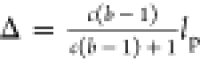 . Then, to realize a long-range formation
of the 1-D adatom structure on a surface, Δ has to satisfy the
condition Δ = rl2 mod lp, where r is an integer. This condition
guarantees the existence of the long-range 1-D quasi-periodic structure,
and the system can be considered as one type of the 1-D quasi-crystal.20−22
. Then, to realize a long-range formation
of the 1-D adatom structure on a surface, Δ has to satisfy the
condition Δ = rl2 mod lp, where r is an integer. This condition
guarantees the existence of the long-range 1-D quasi-periodic structure,
and the system can be considered as one type of the 1-D quasi-crystal.20−22
For the present B/Cu(110) system, the lengths for the two equations were lp = 2.6 and l2 = 5.4 Å, and the concentration was determined to be c = 0.25 from the STM images. Then, the obtained value of Δ = 0.22 Å consistently matches that of rl2 mod lp with r = 1. Thus, the present 1-D structure meets the quasi-periodic condition and could be possibly regarded as a 1-D quasi-crystal20−22 with their long-range existence. It is worth mentioning that assignments of the 1-D quasi-crystal have been controversial compared to the higher dimensional quasi-crystals that can include the definite geometrical condition (e.g., 5-fold rotational symmetry).18 Theoreticians have developed various models of the 1-D quasi-crystal, such as Fibonacci quasi-crystal and incommensurate structure with no average lattice.20−24 The experimental results here demonstrate that a solid surface is an appropriate way to examine the actual material.
The complexity of the quasi-periodic structure along the intrachain direction makes it difficult to directly determine the appropriate structure model by first-principles calculation, for example. On the other hand, the periodic structure along the interchain direction, being commensurate with the Cu(110) lattice, may provide a significant point of view of the surface atomic arrangement. Along the [001] direction, an array of the atomic chain has a period of 1.1 nm that corresponds to 3a[001], as described in Figure 1. Figure 3a shows an STM image, and Figure 3b presents a set of the two line profiles across the bright and dark regions in the quasi-periodic chains. An interval between the two characteristic protrusions was 3.51 Å, while the distance between the protrusion and the valley was 3.71 Å (Figure 3b). Both of them are close to the Cu(110) unit cell length of a[001] = 3.61 Å. Based on these characteristic features, a structural model can be considered as depicted in Figure 3c. Valleys in the line profiles (trenches in the image) are likely assigned to missing Cu atoms (rows) on the Cu(110) surface, and the 1-D B/Cu(110) structure has a basic framework of a pair of the Cu rows. The atomic structure is inherently commensurate along the [001] direction with the Cu(110) lattice. The bright region in the STM images has the unit length of l2 = 5.4 Å that can embed 1–3 boron atoms, according to the interatomic boron distances, reported previously.6 A possible Cu boride model, presented in Figure 3c, is energetically optimized,15 and it is confirmed to be stable over a picosecond by the molecular dynamics simulation. The STM simulation of the cross section reproduces the valley feature in the line profiles in Figure 3b. The bright and dark regions in the STM image themselves are simulated successfully, as shown in Figure 3d. The consistency between the experiment and the calculation ensures that the bright region is associated with the boron adsorbates that form the copper borides, while the dark region exposes the bare copper surface that is reconstructed. STM simulations of other possible atomic models are given in the Supporting Information which confirms the present assignment of the image appearance.
Figure 3.

STM simulation of Cu atomic configuration and proposed structural models (a) STM image and (b) intensity line profile taken from the [001] direction crossing different bright (3.–4.) and dark (1.–2.) regions as indicated in white lines. (c) Structural model and local density of states (LDOS) calculated for the STM simulations at sample bias +1.5 and −1.5 V cut by the red line for side view. (d) STM simulation of calculated based on the structural model.15 Green balls represent the boron atoms, while light gray, gray, and black represent the first, second, and third (or substrate) layers of Cu atoms, respectively.
The actual growth observed by the STM was an 1-D growth in a self-assembled manner, which forms a taenioid domain growing in the [11̅0] direction, even extending the terrace edge, as stated in Figure 1. Based on a structure model of the reconstructed Cu surface (Figure 3), Figure 4 schematically describes the sequential growth processes at the surface step based on the three-layer model. It is of note that the X-ray photoemission spectroscopy (XPS) result of the 3 × 1-B/Cu(110)14 phase showed a similar spectra of the Cu-Boride on Cu(111) suggesting this phase to be another Cu-Boride compound, which is in good agreement with the proposed structural model and growth mode extending the Cu terrace. On the Cu(110) surface, copper atoms in the first (topmost) layer sit at hollow sites on the second layer, and the step structure is illustrated in Figure 4a. Formation of the 1-D structure was associated with the atomic trench that led to the 3-fold periodicity along the [001] axis, as observed in Figure 1e. Thus, it required the mass transport of Cu atoms elsewhere to form the surface structure. Extension of the 1-D domain over the step, observed in Figure 4b, indicated that Cu atoms sequentially in the first layer diffused onto the lower terrace (Figure 4c,d), forming the atomic trenches and the Cu-Boride chain sequentially by connecting at the edge and expanding its length, as shown in Figure 4e. The anisotropic domain extended over 200 nm, as shown in Figure 4b (STM image).
Figure 4.

A sequence of one-dimensional (1-D) structure growth at a Cu(110) step. (a) The initial step structure on a clean Cu(110) surface. The corresponding STM image was taken with It = 100 pA and Vs = −1.5 V. (b) STM image after growth of the 1-D B/Cu(110) structure (It = 150 pA, Vs = 1.5 V). (c–e) The atomic model composed of three Cu layers colored in light-gray (first), gray (second), and black (third). The green and red regions respectively represent the synthesized Cu-Boride and Cu-Boride undergoing synthesis. (c) A pristine step on the Cu(110) surface. (d) Diffusion of copper atoms and the connection with the edge. (e) Extension of the 1-D structure, resulting in anisotropic domain growth on the lower terrace.
The growth of the 1-D atomic structure was in contrast to that of other structures on Cu(110). For example, the well-known CuO chain of the O/Cu(110) phase grows parallel to the [001] direction according to the steps,25−28 which is orthogonal to the 1-D direction of the present B/Cu(110) phase.14 The peculiarity of B/Cu(110) most likely originates from the thermal stability of the quasi-periodic 1-D structure or the kinetics of its formation. The connection of the diffused adatom at the chain end has been critical for 1-D growth on semiconductor surfaces.29,30 The extensions were promoted when the edge became an activation site and was induced by the localized state at the terminus, such as dangling bonds.29,30 The long-scale growth of the 1-D domain of B/Cu(110) indicates that existence of the active site at the end. It is worth mentioning from the previous theoretical and experimental research that the quasi-1D crystal has a topological edge state at the end.31−33 The topological attributes of the 1-D quasi-crystallinity may have contributed to the growth of Cu-Boride chains over several 100 nm. While the quasi-periodic 1D structure of the B/Cu(110) system requires much effort to unveil the precise atomic structure, the present system may become a significant playground to examine the exotic properties of topological materials. Moreover, previous studies of Cu-Boride on Cu(111)6 confirmed that the surface phase was arranged of alternating 1-D atomic chains. The relationship between the 1-D boron and the surface is an intriguing issue in metallurgy and boron science.34
Formations of the borophene35,36 or 2D copper boride layers on Cu(111)5,37 and Cu(100)38 have been reported previously, which is in contrast to the quasi-periodic 1D boron structure on Cu(110). Difference of the growth may be understood in terms of the structural difference in the Cu crystal surfaces themselves. The Cu(110) surface has the 2-fold rotational symmetry, while the Cu(111) and Cu(100) surfaces have 3-fold and 4-fold rotational symmetry, respectively. Thus, the Cu(110) substrate inherently has the 1-D anisotropy, while the other two substrates behave 2-D. This unique character allows growth of the 1-D structure, and it has been well-known on Cu(110) with various adsorbates.12,26 Another important uniqueness of Cu(110) is that the interlayer distance, d110 = 1.28 Å, is shorter than the other copper crystal surface, d111 = 2.09 Å and d100 = 1.81 Å. It is inferred that the mass transport of copper atom occurs at Cu(110) much easier than at Cu(111) and Cu(100) by adsorbate-induced surface reconstruction. These two unique characteristics of Cu(110) may describe growth of the 1D boron, which is in contrast to the 2D boron growth on metal substrates.
In summary, we observed a 1-D Cu-Boride system that grew quasi-periodically on a Cu(110) surface. It exhibited robust 1-D growth expanding over several 100 nm, while the unusual structure was indicated to be quasi-periodic via Fourier transform analysis. Further examination based on the Aubry model, which offers conditions for the existence of an incommensurate structure with no average lattice, has provided an understanding of this quasi-periodic 1-D structure, which grows by combining two unit lengths. With its unique growth characteristics and quasi-periodic nature, the 1-D system on the B/Cu(110) surface is an intriguing boron compound and could become a significant way to examine 1-D quasi-crystals.
Methods
Sample Preparation
Samples were prepared on the (110) surface of a commercial Cu crystal (MaTecK, Germany). A clean surface was obtained via cycles of Ar+ sputtering at 0.5 kV and annealing at 600 °C, followed by confirmation with STM and low-energy electron diffraction (LEED). By deposition of boron (99.999% pure) on the Cu(110) surface at 500 °C, we were able to obtain a slight 3 × 1 LEED pattern that corresponded to the B/Cu(110) surface imaged by STM. The LEED pattern with detailed information on condition of the boron deposition is described in refs (14 and 15).
STM Conditions
STM imaging was conducted with a commercial low-temperature STM instrument (Omicron, Germany) with a chemically etched W tip at 80 K by cooling with liquid N2. Topographic STM images were acquired in a constant current (It) mode, and several sample biases (Vs), with the Nanonis SPM control system. The STM images were analyzed with WSxM39 and Gwyddion16 software. All procedures and STM imaging were conducted in an ultrahigh-vacuum chamber with the base pressure below 1.0 × 10⁻¹⁰ Torr.
STM Simulation
Surface optimizations and constant-current STM simulations were performed via Quantum ESPRESSO v6.7, a first-principles code based on density functional theory using the plane-wave and the pseudopotential method.40−42 The calculations used the GGA-PBE exchange-correlation functional43 with ultrasoft pseudopotentials from the SSSP Efficiency v1.1.2 library.44 The cutoff energies for the plane-wave basis and the charge density were set to 70 and to 600 Ry, respectively. For surface optimizations, the convergence criteria for force and total energy were set to 1.0 × 10⁻⁴ Ry and 4.2 × 10⁻⁴ Ry/bohr, respectively. For Brillouin zone integration, we performed k-point sampling using the Monkhorst–Pack method, ensuring that the finite difference of the k-point was equal to or below 0.20 (1/Å).45 Simulations of filled- and empty-state STM images were performed by following the Tersoff–Hamann approximation, as implemented in Quantum ESPRESSO.46
Molecular Dynamics Simulation
The thermodynamic stability of the slab model structure was verified by Born–Oppenheimer molecular dynamics simulation, implemented in Quantum ESPRESSO. In this simulation, the ion temperature was controlled at 300 K using the Andersen thermostat method.47 Slab model employed the effective screening medium method, with the vacuum/slab/vacuum boundary condition.48 The parameters, such as the pseudopotential and the cutoff energy, are the same as those adopted in the STM simulation.
Acknowledgments
This work was supported by JSPS KAKENHI grants (Grants No. JP21H05012, No. JP19H04398, and No. JP18H03874), by a Grant-in-Aid for JSPS Fellows (Grant No. 21J21993), and by JST, CREST Grant No. JPMJCR21O4, Japan. We acknowledge Keiichi Edagawa, Ryuji Tamura, and Kaoru Kimura for valuable discussion on quasi-crystals. We are thankful to Yanze Guan, Claudio Backes, Izumi Mochizuki, and Ken Wada for electron diffraction experiments of the samples at the SPF beamline in KEK.
Supporting Information Available
The Supporting Information is available free of charge at https://pubs.acs.org/doi/10.1021/acs.nanolett.3c03861.
Quasi-periodic growth of one-dimensional copper boride on a surface, which introduces additional information on sample preparation, STM bias dependence, STM simulation, analysis of 2-D FFT, 1-D FFT, simulation of the Laue function, and conditions for realizing the 1-D quasi-crystals (PDF)
The authors declare no competing financial interest.
Supplementary Material
References
- Krawiec M. Functionalization of Group-14 Two-Dimensional Materials. J. Phys.: Condens. Matter 2018, 30, 233003. 10.1088/1361-648X/aac149. [DOI] [PubMed] [Google Scholar]
- Kaneti Y. V.; Benu D. P.; Xu X.; Yuliarto B.; Yamauchi Y.; Golberg D. Borophene: Two-dimensional Boron Monolayer: Synthesis, Properties, and Potential Applications. Chem. Rev. 2022, 122, 1000–1051. 10.1021/acs.chemrev.1c00233. [DOI] [PubMed] [Google Scholar]
- Molle A.; Goldberger J.; Houssa M.; Xu Y.; Zhang S.-C.; Akinwande D. Buckled Two-Dimensional Xene Sheets. Nat. Mater. 2017, 16, 163–169. 10.1038/nmat4802. [DOI] [PubMed] [Google Scholar]
- Deng J.; Xia B.; Ma X.; Chen H.; Shan H.; Zhai X.; Li B.; Zhao A.; Xu Y.; Duan W.; Zhang S.-C.; Wang B.; Hou J. G. Epitaxial Growth of Ultraflat Stanene with Topological Band Inversion. Nat. Mater. 2018, 17, 1081–1086. 10.1038/s41563-018-0203-5. [DOI] [PubMed] [Google Scholar]
- Yue C.; Weng X.-J.; Gao G.; Oganov A. R.; Dong X.; Shao X.; Wang X.; Sun J.; Xu B.; Wang H.-T.; Zhou X.-F.; Tian Y. Formation of Copper Boride on Cu(111). Fundamental Research 2021, 1, 482–487. 10.1016/j.fmre.2021.05.003. [DOI] [Google Scholar]
- Tsujikawa Y.; Horio M.; Zhang X.; Senoo T.; Nakashima T.; Ando Y.; Ozaki T.; Mochizuki I.; Wada K.; Hyodo T.; Iimori T.; Komori F.; Kondo T.; Matsuda I. Structural and Electronic Evidence of Boron Atomic Chains. Phys. Rev. B 2022, 106, 205406. 10.1103/PhysRevB.106.205406. [DOI] [Google Scholar]
- Weng X.-J.; Bai J.; Hou J.; Zhu Y.; Wang L.; Li P.; Nie A.; Xu B.; Zhou X.-F.; Tian Y. Experimental Evidence of Surface Copper Boride. Nano Research 2023, 16, 9602–9607. 10.1007/s12274-023-5496-2. [DOI] [Google Scholar]
- Akopov G.; Yeung M. T.; Kaner R. B. Rediscovering the Crystal Chemistry of Borides. Adv. Mater. 2017, 29, 1604506. 10.1002/adma.201604506. [DOI] [PubMed] [Google Scholar]
- Weng X.-J.; He X.-L.; Hou J.-Y.; Hao C.-M.; Dong X.; Gao G.; Tian Y.; Xu B.; Zhou X.-F. First-Principles Prediction of Two-Dimensional Copper Borides. Phys. Rev. Mater. 2020, 4, 074010. 10.1103/PhysRevMaterials.4.074010. [DOI] [Google Scholar]
- Yu X.; Sun Q.; Liu M.; Du W.; Liu Y.; Cai L.; Zha Z.; Pan J.; Kang F.; Gao W.; Yang D.; Qiu X.; Xu W. Lattice-Directed Selective Synthesis of Acetylenic and Diacetylenic Organometallic Polyynes. Chem. Mater. 2022, 34, 1770–1777. 10.1021/acs.chemmater.1c04015. [DOI] [Google Scholar]
- Do E.; Park J. W.; Stetsovych O.; Jelinek P.; Yeom H. W. Z3 Charge Density Wave of Silicon Atomic Chains on a Vicinal Silicon Surface. ACS Nano 2022, 16, 6598–6604. 10.1021/acsnano.2c00972. [DOI] [PMC free article] [PubMed] [Google Scholar]
- Lipton-Duffin J. A.; Miwa J. A.; Kondratenko M.; Cicoira F.; Sumpter B. G.; Meunier V.; Perepichka D. F.; Rosei F. Step-by-Step Growth of Epitaxially Aligned Polythiophene by Surface-Confined Reaction. Proc. Natl. Acad. Sci. U. S. A. 2010, 107, 11200–11204. 10.1073/pnas.1000726107. [DOI] [PMC free article] [PubMed] [Google Scholar]
- Xia Y.; Yang P.; Sun Y.; Wu Y.; Mayers B.; Gates B.; Yin Y.; Kim F.; Yan H. One-Dimensional Nanostructures: Synthesis, Characterization, and Applications. Adv. Mater. 2003, 15, 353–389. 10.1002/adma.200390087. [DOI] [Google Scholar]
- Tsujikawa Y.; Zhang X.; Horio M.; Wada T.; Miyamoto M.; Sumi T.; Komori F.; Kondo T.; Matsuda I. Observing an Ordered Surface Phase by B Deposition on Cu(110). Surf. Sci. 2023, 732, 122282. 10.1016/j.susc.2023.122282. [DOI] [Google Scholar]
- Supporting Information.
- Nečas D.; Klapetek P. Gwyddion: an open-source software for SPM data analysis. Central European Journal of Physics 2012, 10, 181–188. 10.2478/s11534-011-0096-2. [DOI] [Google Scholar]
- Steinhardt P. J.; Ostlund S.. The Physics of Quasicrystals; World Scientific Pub. Co. Inc.: Singapore, 1987; pp 1–15. [Google Scholar]
- Walter S.; Deloudi S.. Crystallography of Quasicrystals: Concepts, Methods and Structures; Springer Series in Materials Science; Springer Berlin Heidelberg: Berlin, Heidelberg, 2009; Vol. 126. [Google Scholar]
- Ziman J. M.Models of Disorder; The Theoretical Physics of Homogeneously Disordered Systems; Cambridge University Press: 1979. [Google Scholar]
- Aubry S.; Godrèche C.; Vallet F. Incommensurate Structure with No Average Lattice: an Example of a One-Dimensional Quasicrystal. J. Phys. (Paris) 1987, 48, 327–334. 10.1051/jphys:01987004803032700. [DOI] [Google Scholar]
- Aubry S.; Godrèche C. Incommensurate Structure with No Average Lattice: An Example of a One-Dimensional Quasicrystal. Journal de Physique Colloques 1986, 47, 187–196. 10.1051/jphyscol:1986319. [DOI] [Google Scholar]
- Godrèche C.; Luck J. M.; Vallet F. Quasiperiodicity and Types of Order; a Study in One Dimension. Journal of Physics A: Mathematical and General 1987, 20, 4483. 10.1088/0305-4470/20/13/047. [DOI] [Google Scholar]
- Jagannathan A. The Fibonacci Quasicrystal: Case Study of Hidden Dimensions and Multifractality. Rev. Mod. Phys. 2021, 93, 045001. 10.1103/RevModPhys.93.045001. [DOI] [Google Scholar]
- Kohmoto M.; Sutherland B.; Tang C. Critical Wave Functions and a Cantor-set Spectrum of a One-Dimensional Quasicrystal Model. Phys. Rev. B 1987, 35, 1020–1033. 10.1103/PhysRevB.35.1020. [DOI] [PubMed] [Google Scholar]
- Jensen F.; Besenbacher F.; Laegsgaard E.; Stensgaard I. Surface Reconstruction of Cu(110) Induced by Oxygen Chemisorption. Phys. Rev. B 1990, 41, 10233–10236. 10.1103/PhysRevB.41.10233. [DOI] [PubMed] [Google Scholar]
- Kuk Y.; Chua F. M.; Silverman P. J.; Meyer J. A. O Chemisorption on Cu(110) by Scanning Tunneling Microscopy. Phys. Rev. B 1990, 41, 12393–12402. 10.1103/PhysRevB.41.12393. [DOI] [PubMed] [Google Scholar]
- Coulman D. J.; Wintterlin J.; Behm R. J.; Ertl G. Novel Mechanism for the Formation of Chemisorption Phases: The (2 × 1)O-Cu(110) “added Row” Reconstruction. Phys. Rev. Lett. 1990, 64, 1761–1764. 10.1103/PhysRevLett.64.1761. [DOI] [PubMed] [Google Scholar]
- Kern K.; Niehus H.; Schatz A.; Zeppenfeld P.; Goerge J.; Comsa G. Long-Range Spatial Self-Organization in the Adsorbate-Induced Restructuring of Surfaces: Cu{100}-(2 × 1)O. Phys. Rev. Lett. 1991, 67, 855–858. 10.1103/PhysRevLett.67.855. [DOI] [PubMed] [Google Scholar]
- Evans M. M. R.; Nogami J. Indium and Gallium on Si(001): A Closer Look at the Parallel Dimer Structure. Phys. Rev. B 1999, 59, 7644–7648. 10.1103/PhysRevB.59.7644. [DOI] [Google Scholar]
- Brocks G.; Kelly P. J.; Car R. Adsorption of Al on Si(100): A Surface Polymerization Reaction. Phys. Rev. Lett. 1993, 70, 2786–2789. 10.1103/PhysRevLett.70.2786. [DOI] [PubMed] [Google Scholar]
- Lang L.-J.; Cai X.; Chen S. Edge States and Topological Phases in One-Dimensional Optical Superlattices. Phys. Rev. Lett. 2012, 108, 220401. 10.1103/PhysRevLett.108.220401. [DOI] [PubMed] [Google Scholar]
- Kraus Y. E.; Lahini Y.; Ringel Z.; Verbin M.; Zilberberg O. Topological States and Adiabatic Pumping in Quasicrystals. Phys. Rev. Lett. 2012, 109, 106402. 10.1103/PhysRevLett.109.106402. [DOI] [PubMed] [Google Scholar]
- Ganeshan S.; Sun K.; Das Sarma S. Topological Zero-Energy Modes in Gapless Commensurate Aubry-André-Harper Models. Phys. Rev. Lett. 2013, 110, 180403. 10.1103/PhysRevLett.110.180403. [DOI] [PubMed] [Google Scholar]
- Matsuda I., Wu K., Eds. 2D Boron: Boraphene, Borophene, Boronene; Springer International Publishing: Cham, 2021. [Google Scholar]
- Liu Y.; Penev E. S.; Yakobson B. I. Probing the Synthesis of Two-Dimensional Boron by First-Principles Computations. Angew. Chem., Int. Ed. 2013, 52, 3156–3159. 10.1002/anie.201207972. [DOI] [PubMed] [Google Scholar]
- Zhang Z.; Yang Y.; Gao G.; Yakobson B. I. Two-Dimensional Boron Monolayers Mediated by Metal Substrates. Angew. Chem., Int. Ed. 2015, 54, 13022–13026. 10.1002/anie.201505425. [DOI] [PubMed] [Google Scholar]
- Wu R.; Drozdov I. K.; Eltinge S.; Zahl P.; Ismail-Beigi S.; Božović I.; Gozar A. Large-Area Single-Crystal Sheets of Borophene on Cu(111) Surfaces. Nat. Nanotechnol. 2019, 14, 44–49. 10.1038/s41565-018-0317-6. [DOI] [PubMed] [Google Scholar]
- Wu R.; Eltinge S.; Drozdov I. K.; Gozar A.; Zahl P.; Sadowski J. T.; Ismail-Beigi S.; Božović I. Micrometre-Scale Single-Crystalline Borophene on a Square-Lattice Cu(100) Surface. Nat. Chem. 2022, 14, 377–383. 10.1038/s41557-021-00879-9. [DOI] [PubMed] [Google Scholar]
- Horcas I.; Fernández R.; Gómez-Rodríguez J. M.; Colchero J.; Gómez-Herrero J.; Baro A. M. WSXM: A Software for Scanning Probe Microscopy and a Tool for Nanotechnology. Rev. Sci. Instrum. 2007, 78, 013705. 10.1063/1.2432410. [DOI] [PubMed] [Google Scholar]
- Hohenberg P.; Kohn W. Inhomogeneous Electron Gas. Phys. Rev. 1964, 136, B864–B871. 10.1103/PhysRev.136.B864. [DOI] [Google Scholar]
- Kohn W.; Sham L. J. Self-Consistent Equations Including Exchange and Correlation Effects. Phys. Rev. 1965, 140, A1133–A1138. 10.1103/PhysRev.140.A1133. [DOI] [Google Scholar]
- Giannozzi P.; et al. QUANTUM ESPRESSO: A Modular and Open-Source Software Project for Quantum Simulations of Materials. J. Phys.: Condens. Matter 2009, 21, 395502. 10.1088/0953-8984/21/39/395502. [DOI] [PubMed] [Google Scholar]
- Perdew J. P.; Burke K.; Ernzerhof M. Generalized Gradient Approximation Made Simple. Phys. Rev. Lett. 1996, 77, 3865–3868. 10.1103/PhysRevLett.77.3865. [DOI] [PubMed] [Google Scholar]
- Prandini G.; Marrazzo A.; Castelli I. E.; Mounet N.; Marzari N. Precision and Efficiency in Solid-State Pseudopotential Calculations. npj Computational Materials 2018, 4, 1–13. 10.1038/s41524-018-0127-2. [DOI] [Google Scholar]
- Monkhorst H. J.; Pack J. D. Special Points for Brillouin-zone Integrations. Phys. Rev. B 1976, 13, 5188–5192. 10.1103/PhysRevB.13.5188. [DOI] [Google Scholar]
- Tersoff J.; Hamann D. R. Theory of the Scanning Tunneling Microscope. Phys. Rev. B 1985, 31, 805–813. 10.1103/PhysRevB.31.805. [DOI] [PubMed] [Google Scholar]
- Andersen H. C. Molecular Dynamics Simulations at Constant Pressure and/or Temperature. J. Chem. Phys. 1980, 72, 2384–2393. 10.1063/1.439486. [DOI] [Google Scholar]
- Otani M.; Sugino O. First-Principles Calculations of Charged Surfaces and Interfaces: A Plane-Wave Nonrepeated Slab Approach. Phys. Rev. B 2006, 73, 115407. 10.1103/PhysRevB.73.115407. [DOI] [Google Scholar]
Associated Data
This section collects any data citations, data availability statements, or supplementary materials included in this article.