

Abstract

Metasurfaces have recently risen to prominence in optical research, providing unique functionalities that can be used for imaging, beam forming, holography, polarimetry, and many more, while keeping device dimensions small. Despite the fact that a vast range of basic metasurface designs has already been thoroughly studied in the literature, the number of metasurface-related papers is still growing at a rapid pace, as metasurface research is now spreading to adjacent fields, including computational imaging, augmented and virtual reality, automotive, display, biosensing, nonlinear, quantum and topological optics, optical computing, and more. At the same time, the ability of metasurfaces to perform optical functions in much more compact optical systems has triggered strong and constantly growing interest from various industries that greatly benefit from the availability of miniaturized, highly functional, and efficient optical components that can be integrated in optoelectronic systems at low cost. This creates a truly unique opportunity for the field of metasurfaces to make both a scientific and an industrial impact. The goal of this Roadmap is to mark this “golden age” of metasurface research and define future directions to encourage scientists and engineers to drive research and development in the field of metasurfaces toward both scientific excellence and broad industrial adoption.
Keywords: metasurface, metalens, flat optics, inverse and topological design, computational imaging, tunable metasurfaces, new concepts, emerging material platforms, large-scale nanofabrication, metasurface applications
1. Introduction
Arseniy I. Kuznetsov and Mark L. Brongersma
Optical metamaterials, which are artificial materials composed of light-scattering nanostructures with engineered optical properties, have long been sought after by scientists in various fields of physics and engineering. While the first theoretical discussions of such materials date back to 1940s, their rapid experimental development has only started around 20−30 years ago driven by rapid advances in nanotechnology and semiconductor manufacturing. The early theoretical studies in this field primarily considered 3D bulk nanostructured materials, but most of the experimental efforts in the optical domain have been directed toward essentially flat, nanostructured optical elements that can be realized by single- or a few-step lithographic processes. It was soon appreciated that these two-dimensional (2D) elements, now termed metasurfaces, can be used to control light in unprecedented fashion due to a rapid nanoscale phase and amplitude change imprinted to light waves by each individual nanostructure. Interested readers are encouraged to look through some excellent reviews of this field, which can help to trace its explosive development over the past decades.1−6 Recent demonstrations in this field have shown that even a single-layer metasurface can efficiently bend or focus light, generate complex holograms and wavefronts, and control polarization of light in a previously unachievable fashion with much higher spatial resolution, thus, at higher diffraction angles/numerical apertures, as compared to conventional diffractive optical elements. This has triggered a strong and constantly growing interest from various industries that greatly benefit from the availability of miniaturized and highly efficient optical components, which can more easily be integrated in optoelectronic systems at low cost. Research on optical metasurfaces is currently flourishing as it is evolving from simple optical functionalities to complex optical systems and spreading into various adjacent fields, including computational imaging, augmented and virtual reality, automotive, display, biosensing, nonlinear, quantum and topological optics, optical computing, and more. The first industrial products have also been announced, driving rapid development of large-scale and low-cost manufacturing that will allow for the broad adoption of the metasurface-based flat optics technology. The strong scientific efforts that coincide with substantial industrial demand are creating a truly unique opportunity for the field of metasurfaces and metamaterials. The goal of this Roadmap is to highlight the broad diversity of opportunities and drive the metasurface research and technology development toward future impact (see Figure 1).
Figure 1.

Road ahead for optical metasurfaces.
This Roadmap consists of seventeen sections highlighting different future directions of science and technology development for optical metasurfaces. Following this brief introduction (Section 1), we will first focus on the key applications of metasurface technology to imaging, highlighting the challenges and opportunities of metalenses for aberration-free imaging with diffraction limited resolution (Section 2) as well as super-resolution imaging for picophotonics (Section 3). We will then continue with a discussion of other metasurface functionalities that capitalize on effective phase, amplitude, and polarization control (Sections 4 and 5). We end this part with an analysis of more complex multilayered flat optical elements and multielement meta-optics systems (Section 6). We will then proceed by surveying the application of emerging computational methods, such as machine learning and inverse design, to complement the metasurface design capabilities (Section 7) as well as to process metalens-obtained images to improve their quality (Section 8). We will also describe how metasurfaces themselves can be used for optical computing (Section 9). Then, from passive flat optical components we switch to active metasurface devices, in particular, focusing on tunable metasurfaces that can control the wavefront of light dynamically (Section 10), as well as on those that can either help to emit or detect light in optoelectronic devices (Section 11). Finally, we will focus on more advanced concepts of metasurface research including nonlinear (Section 12), quantum (Section 13), topological, nonlocal, and other new directions (Section 14). The research roadmap is complemented by a discussion of novel material platforms (Section 15) and large-scale manufacturing methodologies (Section 16) for optical metasurfaces as well as industry perspective for the field (Section 17).
2. Meta-Lenses: Concepts, Implementations, and Applications
Jin Yao, Mu Ku Chen, Uriel Levy, and Din Ping Tsai
2.1. Current State of the Art
2.1.1. Introduction
Meta-lenses have attracted tremendous attention due to their compact size and flexibility in manipulating light as compared to conventional lenses. Benefiting from novel design concepts and advanced implementation techniques, various applications have been developed based on meta-lenses, such as focusing, imaging, sensing, polarization detection, and nonlinear generation, as shown in Figure 2.
Figure 2.

Concepts, implementations, and applications of meta-lenses. Full-color routing: Reproduced with permission from ref (13). Copyright 2017 American Chemical Society. Achromatic imaging: Reproduced with permission from ref (14). Copyright 2018 Springer Nature. Biomedical imaging: Reproduced with permission from ref (15). Copyright 2021 American Chemical Society. Edge detection: Reproduced with permission from ref (18). Copyright 2021 De Gruyter. Phase sensing: Reprinted or adapted with permission under a Creative Commons CC-BY 4.0 from ref (19). Copyright 2021 Springer Nature. Polarization detection: Reproduced with permission from ref (20). Copyright 2018 American Chemical Society. Nonlinear generation: Reprinted or adapted with permission under a Creative Commons CC-BY 4.0 from ref (22). Copyright 2022 American Association for the Advancement of Science. Quantum source: Reproduced with permission from ref (23). Copyright 2020 American Association for the Advancement of Science.
2.1.2. Concepts
A meta-lens can manipulate the incident planar wavefront to focus light by effectively selecting and arranging meta-atoms. Various phase profiles have been demonstrated for functional focusing and imaging. The hyperbolic phase profile is originally free of spherical aberration, beneficial for high numerical aperture (NA) focusing, while restricted by strong coma aberrations in imaging configuration. Recently it was shown that a quadratic phase profile can give wide field of view (FOV) imaging, avoiding coma aberration, but suffers from spherical aberrations.7 Even better imaging with meta-lenses can be achieved by computer-optimized phase profiles, which is a promising direction for advanced meta-lens design (see Section 2.3 and Section 7). According to different operating mechanisms to imprint a phase on an incident light wave, the design principles for a meta-lens can be classified into four categories that are listed below.
2.1.2.1. Geometric Phase
The geometric phase, also known as the Pancharatnam−Berry (P-B) phase, is based on the spatial symmetry of the meta-atom local field. The sudden phase change φ = −2σθ of the electromagnetic wave can be generated by adjusting the rotation angle θ of the meta-atom, where σ = ±1 represents the state of left- or right-handed circularly polarized light, respectively. The use of the geometric phase can greatly reduce the complexity of meta-lens design, offering more freedom for wavefront manipulation. To achieve high diffraction and polarization conversion efficiencies, geometric phase meta-lenses generally require resonant or high aspect ratio meta-atoms.8
2.1.2.2. Propagation Phase
The propagation
phase (also known as the truncated waveguide approach) is produced
by the optical path difference of electromagnetic wave propagation
in different meta-atoms. The accumulated propagation phase 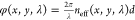 of electromagnetic waves can be flexibly
manipulated by varying the waveguide mode index neff(x,y,λ) of
the truncated guides and the physical propagation length d through the meta-atom, where x and y are spatial coordinates and λ is the wavelength. Benefiting
from the mechanism, the propagation phase meta-lens can be polarization-independent
and efficient. In order to acquire the 2π phase distribution
in practical operations, the refractive index and aspect ratio of
the meta-atom need to be high in general.9
of electromagnetic waves can be flexibly
manipulated by varying the waveguide mode index neff(x,y,λ) of
the truncated guides and the physical propagation length d through the meta-atom, where x and y are spatial coordinates and λ is the wavelength. Benefiting
from the mechanism, the propagation phase meta-lens can be polarization-independent
and efficient. In order to acquire the 2π phase distribution
in practical operations, the refractive index and aspect ratio of
the meta-atom need to be high in general.9
2.1.2.3. Resonance Phase
The resonance phase is the sudden phase change at a resonant wavelength, which can be manipulated by modifying the meta-atom geometry. First resonance phase meta-lenses had the problems of narrow bandwidth and low efficiency. Later, the efficiency was improved in Huygens’ meta-lenses based on the Kerkers’ condition, which can achieve a 2π phase shift. Their fundamental limitations, such as reciprocity, multimode/monomode operation, and symmetry breaking should be carefully considered.10 Integrated-resonant units (IRUs) that incorporate multiple resonators and resonances into one meta-atom, can efficiently engineer the phase distribution across a continuous, broad spectral range. The aspect ratio of these structures is typically lower than those of optical elements that rely on a propagation phase.
Furthermore, associating two or more types of phase mechanisms can boost the multifunctionality and performance of a meta-lens. Independent phase control for each circular polarization can be realized by combining the propagation phase with the geometric phase. Merging geometric and resonance phases can also provide an effective strategy for the wideband reflective and transmissive achromatic meta-lenses.
2.1.3. Practical Implementations
The fabrication of meta-lenses can be generally categorized in several ways. The layout of the meta-lenses can be transferred to a mask layer or a target material. By using the mask layer, the pattern prepared by electron-beam lithography (EBL) and photolithography is further transferred to the target material via an etch process. The layout can also be directly created by focused-ion-beam (FIB) milling, nanoimprinting, 3D printing, laser direct writing, etc. The choice of implementation method needs to take into account the fabrication requirements of the meta-lenses. The target material selection, sample size, unit-cell feature size, and structure complexity have to be considered. The critical dimensions and empirical parameters of processes are helpful for the fabrication selection of the meta-lens implementation.
2.1.4. Applications
2.1.4.1. Focusing of Light
When the meta-lens is employed in optical systems, its focusing properties require to be considered and modified. Diffraction-limited focusing and extra-high NA focusing are significant for applications requiring small light−matter interaction volume or large angular collection. Kuznetsov et al. proposed a novel concept based on diffracted energy redistribution by nanoantenna inclusions with asymmetric scattering patterns. A diffraction-limited meta-lens with a near-unity NA > 0.99 and subwavelength thickness of ∼λ/3 was demonstrated to operate upon unpolarized excitation at 715 nm. This work can efficiently bend light at angles as large as 82°, which are not achievable with conventional bulk optics.11 Dispersive properties of monochromatic meta-lenses can be another interesting property to highlight from a potential application standpoint. On the other hand, achromatic meta-lenses might be much more attractive from the point of view of imaging applications. Capasso et al. demonstrated an achromatic meta-lens by engineering the phase and dispersion of titanium dioxide (TiO2) nanopillars on a dielectric spacer above a metallic mirror.12 An optimization algorithm was utilized to select the nanopillars simultaneously possessing identical phases but distinct dispersions at desired wavelengths. The achromatic meta-lens realizes a constant focal length from 490 to 550 nm with 0.2 NA and 15% diffraction efficiency. To extend the versatility and efficiency of the meta-lens, the multiplex color router has been proposed with a GaN meta-lens integrating four out-of-plane focusing meta-lenses.13 Three primary colors at 430, 532, and 633 nm can be focused to the desired spatial positions with efficiencies of 87%, 91.6%, and 50.6%, respectively. This technology provides great potential for metal-oxide-semiconductor (CMOS) sensor applications.
2.1.4.2. Imaging
Imaging brings the focusing ability of meta-lenses to practical applications. FOV is a crucial parameter in imaging systems, which is generally limited by the compromise with high NA. Kuznetsov et al. analyzed this problem of quadratic metalens and demonstrated wide FOV imaging with a focusing efficiency of 8% and FOV of about 100°. Full imaging of a 5 mm fingerprint with features of about 100 μm was experimentally captured at a distance of 2.5 mm. This work realized the most compact imaging system for fingerprint detection to date. High-quality images also require achromatic meta-lenses to achieve full-color imaging. Tsai et al. developed the strategy of IRU to achieve the broadband achromatic meta-lens, which is comprised of GaN nanopillars and their inverse structures.14 The operating range (400−660 nm) nearly covers the visible region. Full-color imaging can be achieved with a high average efficiency of 40% and an NA = 0.106. The meta-lens is also a preeminent candidate for high-resolution biomedical imaging. A configurable GaN meta-lens has been implemented to realize high-contrast optical sectioning in fluorescence imaging.15 The imaging performance can achieve a lateral resolution of around 2 μm and an optical sectioning capability of around 7 μm. Levy et al. implemented the first meta-lens for outdoor imaging in external passive lighting conditions (sun illumination).16 A detailed discussion regarding the limits of achieving broadband imaging with meta-lenses is given by Levy et al.17
2.1.4.3. Sensing
Light-field sensing and imaging can capture the high-dimensional information of objects, such as depth and edge. A 60 × 60 GaN achromatic meta-lens array has been reported to capture the light-field information. Rendered images with different depths can reconstruct the depth of the object. This system possesses a diffraction-limited resolution of 1.95 μm with incoherent white light incidence. Light-field edge detection was further demonstrated based on a GaN meta-lens array.18 The focused edge images and depth information of objects from 1D to 3D can be extracted by the differentiated and rendering algorithm. This device exhibits the advantages of broadband, data volume reduction, and device miniaturization. Sensing the phase distribution of meta-lenses is also significant, which can connect the design and fabrication processes. Tsai et al. proposed an interferometric imaging phase measurement system to realize the phase sensing of the meta-lens through only one photo.19 Both geometric phase meta-lenses and propagation phase meta-lenses are demonstrated at different wavelengths. The phase measurement was exploited to comprehensively characterize these meta-lenses and its accuracy can achieve 0.05 rad.
2.1.4.4. Polarization Detection
Polarization detection and imaging based on polarization-dependent meta-lenses can provide higher polarization contrast ratios and more compact sizes than conventional optical systems. Three polarization states can be split and focused to six different domains on an image sensor by designing a metasurface device integrating three meta-lenses.20 The polarization state can be detected by measuring four Stokes parameters for each domain. This device can form the image of the complicated polarization object, exhibiting the capability of making a full-Stokes polarization camera. Another direction of polarization detection is to combine it with meta-lens imaging. Capasso et al. demonstrated the chiral imaging capability and the spatially resolved chiral spectroscopy by TiO2 meta-lens with a geometric phase design.21 Two images with opposite helicities of a biological specimen can be simultaneously generated within the same FOV, without the addition of dispersive polarizers.
2.1.4.5. Nonlinear Generation
The functionality of meta-lenses can be extended to nonlinear generation and quantum photonics. Nonlinear imaging by harmonic generation from nonlinear meta-lenses with specific symmetry meta-atoms has been achieved. Combining both the focusing ability and nonlinear generation of nonlinear meta-lenses, they can be applied as short-wavelength light sources. Halas et al. proposed a 150 nm thick zinc oxide (ZnO) nonlinear meta-lens simultaneously converting 394 nm of light to 197 nm of radiation and focusing the generated vacuum ultraviolet (VUV) light.22 The power density of the VUV light at the focal point is 21 times higher than that on the meta-lens surface. In order to generate a quantum light source with high-dimensional entanglement and multiphoton-state generation, Tsai et al. integrated a 10 × 10 GaN meta-lens array with a 0.5 mm beta barium borate (BBO) crystal to realize a 100-path spontaneous parametric down-conversion photon-pair source.23 Four-photon and six-photon generations are demonstrated with high indistinguishability of photons generated from different meta-lenses. Besides meta-lenses, there are various preeminent metasurfaces and meta-devices that generate, enhance, and manipulate nonlinear and quantum effects (see Sections 12 and 13).
2.2. Challenges and Future Goals
Meta-lenses offer new opportunities for the development of flat, compact, low-weight, and multifunctional meta-devices. However, they are still facing many challenges to satisfy the requirements of practical applications. The focusing efficiency of high-NA meta-lenses is originally restricted by phase discretization and diffraction constraints. Achromatic meta-lenses suffer from small size resulting from large phase compensation and the image quality with ambient white-light illumination. The tradeoff among different performances, such as high NA, high efficiency, large FOV, aberration elimination, and multifunctionalities, needs further consideration and design. Conventional design approaches are still limited by the physical mechanism, degree of freedom, and optimization speed.
2.3. Suggested Directions to Meet Goals
Meanwhile, these challenges provide some potential directions for research and development. (i) To acquire novel properties and more versatile applications, meta-lenses can be integrated into existing photonic devices, such as optical fibers, light field cameras, and vivo imaging systems. Compact meta-lenses and their subsequent applications are expected to replace many conventional diffractive optical elements, which can be employed in different environments apart from on the ground, such as in the sky and under the water. Metalenses can also be combined with other metasurfaces to enhance functionalities such as multispectral imaging and polarimetric imaging. (ii) The building blocks of meta-lens can be tailored by combining multiple IRUs with specific optical properties, which can further constitute their large libraries. Physical phenomena producing effective mode coupling effects, especially for those with strong nonlocal responses, such as Fano resonances and bound states in the continuum, provide the potential for performance enhancement. Two-dimensional and active materials are excellent candidates for functional IRUs with compact size and fast response time. (iii) The design process can be assisted by artificial intelligence technology to quickly obtain the optimal solution. Photons carrying high-dimensional information can effectively expand the bandwidth of data processing. Optical neural network computing associating both artificial intelligence technology and meta-optics can overcome the bottleneck of electronic computing power and computing speed. It is important to understand the advantages of meta-lenses over diffractive lenses.24 It is also essential to test meta-lenses properly,25 and to choose proper metrics for comparing broadband meta-lenses.26 Furthermore, one may even take advantage of the metalens strong chromatic dispersion to mitigate challenging applications such as 3D imaging and depth sensing.27 Eventually, it is crucially important to understand the fundamental limitations of metasurfaces and to properly match its degrees of freedom to the specific application in hand. Finally, metalenses can be integrated with conventional lenses for the purpose of minimizing the thickness of the lens stack or compensating distortions (e.g., compensation of chromatic aberrations originated from the material dispersion).
Looking into the future, we envision that meta-lens will be widely applied in variety of applications, ranging from machine vision, virtual and augmented reality to quantum optical chips and optical computation. In fact, some of these applications are already benefiting from metalenses.
3. Metamaterials for Picophotonics: Deeply Subwavelength Optical Metrology and Localization
Nikolay I. Zheludev
3.1. State of the Art
The photonics community is well aware of the metamaterial superlens which uses a slab of negative index metamaterial to recover evanescent waves from the object in the image plane (see Section 2). Realization of a negative index superlens in the optical part of the spectrum faces a number of steep challenges. However, the metamaterial approach is a practical way of creating a different type of superlenses that does not use evanescent waves but instead creates topologically structured light fields and superoscillatory foci in the far-field from the lens. Such fields are needed for advanced super-resolution metrology and imaging.
The phenomenon of optical superoscillations, first introduced in 200628 and experimentally identified shortly after,29 describes the rapid subwavelength spatial variations in the intensity and phase of light in complex electromagnetic fields formed by interference of several coherent waves. Its discovery stimulated the intense revision of the limits of classical electromagnetism in particular the study of structure of superoscillatory fields in free space using robust metamaterial microinterferometric techniques. They experimentally revealed subwavelength energy hotspots and topological features such as phase singularities, energy backflow, anomalously high wavevectors and identified intriguing similarities of the superoscillatory fields in free space to the evanescent plasmonic fields on metals.30 In the last ten years, the better understanding of superoscillatory light has led to the development of superoscillatory lensing, imaging, and metrology technologies.31
Initially, super-resolution technologies used subwavelength light localizations in superoscillatory fields. Indeed, dielectric or metallic binary nanostructured superoscillatory lenses can create hotspots smaller than allowed by conventional lenses.31 Reconfigurable binary lenses based on phase change materials32 have also been introduced.
The nearly complete design freedom on transmissivity and retardation of the lens mask can be achieved using a metasurface manufactured by well-established nanomanufacturing techniques and are scalable to operate at any wavelength. In such a lens, light is scattered on a planar array of “metamolecules”, individual scatterers providing the prescribed levels of phase delay and scattering amplitude at different radial positions on the lens in such a way that the entire array diffracts light into a superoscillatory hotspot. A plasmonic metamaterial superoscillatory lens that is 40 μm in diameter and contains 8500 metamolecules allows subdiffraction hotspots as small as 0.33λ, large fields of views up to 6λ in diameter and robustly performs in imaging applications with an effective numerical aperture of 1.52 that is unattainable in conventional lenses.33
Far-field, label-free nonintrusive super-resolution imaging and metrology techniques that exploit the high light localization in superoscillatory fields have been developed for biological and nanotechnology imaging tasks.31,34−37 They use a superoscillatory hotspot for illumination of the object and a conventional lens for imaging in the confocal setting. Here, the resolution is limited by the size of the hotspot that, in principle, can be arbitrarily small. However, since the intensity of light in the hotspot polynomialy reduces with its size, the practically achieved resolution was limited by about one-fifth of the wavelength.
3.2. Recent Developments: Picometer Resolution
Considerably higher resolution in metrology and localization is possible by exploiting rapid phase variations in topologically structured superoscillatory fields. Indeed, we introduced the “optical ruler”, an electromagnetic analog of a physical ruler, for nanoscale displacement metrology. The optical ruler is a complex electromagnetic field in which singularities serve as the marks on the scale. It is created by the diffraction of light on a Pancharatnam−Berry phase metasurface, with singularity marks then revealed by high-magnification interferometric observation. The “optical ruler” has been applied to detect mutual displacement of two macroscopic platforms. A displacement resolving power of better than 1 nm (λ/800, where λ is the wavelength of light) at a wavelength of 800 nm has been demonstrated. An optical ruler with dimensions of only a few tens of micrometers offers applications in nanometrology, nanomonitoring, and nanofabrication, particularly in the demanding and confined environment of future smart manufacturing tools.38
Recently we demonstrated that illumination with superoscillatory, topologically structured light allowed localization metrology of nanoscale objects with not yet seen accuracy and precision reaching λ/5000 in a single short measurement.39,40 In experiments with a semiconductor nanowire, we employ a deep learning analysis of the scattering of topologically structured light, which is highly sensitive to the nanowire’s position, Figure 3. This is a noninvasive optical metrology with sub-Brownian absolute errors, down to a few tens of femtometre that is a fraction of the typical size of an atom (Si atom is of 220 pm in diameter). There are several factors contributing to the high resolution of this technique.31 From the perspective of Fourier optics, topologically structured superoscillatory illumination gives access to high local wavevectors and ensures much higher sensitivity of the pattern of scattered light to the small features of the investigated object than unstructured light. From the perspective of information theory, recording of multiple scattering patterns during the training process and imaging provides much more information on the imaged object for the retrieval process than what is available in the lens-generated single image for which the Abbe limit applies. Sparsity of the object and prior knowledge about the object shall also be a helpful factor in imaging simple objects such as a dimer, as this helps the retrieval process, similar to how sparsity facilitates “blind” compressed sensing techniques. The retrieval of the image from its diffraction pattern can be mathematically reduced to solving the Fredholm integral equation. It has been proven mathematically41 that neural networks are very efficient in solving these sort of problems. Indeed, the deep-learning process trained on a large data set creates a powerful and accurate deconvolution mechanism without using explicit information on the phase of the detected signals. Experiments show that larger training sets give higher resolution.
Figure 3.
Measuring picometer nanowire displacements via scattering of topologically structured light (following ref (39)). Incident light is topologically structured. Light scattered from the 100 nm wide nanowire is mapped in transmission through a high-NA microscope objective (not shown). Deeply subwavelength lateral (x-direction) displacements of the wire, controlled by application of a DC bias between the wire and the adjacent edge of the supporting membrane, are quantified via a deep-leaning enabled analysis of single-shot scattering patterns.
3.3. Future Developments
The deeply subwavelength topological metrology and visualization techniques outlined above require the stable synthesis of well-defined topologically structured fields. Generators of such fields could be based on liquid crystal spatial light modulators, digital micromirror devices (DMD) and binary and continuous parameters metasurfaces.
DMDs and liquid crystal spatial light modulators offer dynamic control of the field structure. However, they suffer from flickering noise and thermal instabilities. Moreover, pixelation of these devices at the typical level of 10 μm × 10 μm and larger limits accuracy with which the desired wavefront profile can be synthesized, in particular, at singularities. Although static metasurfaces do not allow dynamic control of the generated field, they have superb stability of generated fields and can be routinely manufactured with nanometric precision using a focused ion beam or high-resolution lithography. They can be deployed in a cost-effective scheme for deeply subwavelength metrology and visualization, for instance, replacing a conventional lens in the illumination channels of a standard optical microscope.
The next challenge is the development of high rate versions of the deeply subwavelength topological metrology and microscopy. Indeed, the rate of measurements will only be limited by the image sensor and a rate of one million frames per second has been achieved with 150pm resolution.415 Metamaterial-enabled noninvasive single-shot optical metrology with sub-Brownian resolution, that can be performed with high frame rate image sensors, opens up the exciting field of picophotonics. This includes the study of Brownian motion thermodynamics of nano-objects, including the ballistic regime;42 the study of Van Der Waals forces and non-Hamiltonian forces in nanomechanics;43,44 configuration chemistry of individual molecules; protein folding; and other dynamic events in macromolecules and nanomachines, such as time crystals.45
4. Flat Optics beyond Lenses: Holograms, Polarization Control, and Multifunctionality
Andrei Faraon, Amir Arbabi, and Nanfang Yu
4.1. Current State of the Art
Lenses are some of the most ubiquitous optical components as they are used in a plethora of imaging systems that impact people’s daily lives. As was discussed in detail in Section 2, a lot of effort has gone into developing metasurface lenses for imaging applications. A lens makes use of the metasurface’s capability to control the phase or the propagation direction of light, generally at a fixed frequency. Phase control can be used to generate arbitrary phase masks that can be utilized, for example, in applications related to computational imaging (see Section 8), optical computing (see Section 9), and wavefront shaping. Besides phase and k-vector, light has other degrees of freedom, like polarization, frequency, and amplitude, and optical metasurfaces can also be used to modify these properties (Figure 4). This opens the opportunity to realize multifunctional optical components that can simultaneously control multiple degrees of freedom. One of the initial examples of multifunctionality is metasurfaces that impose two independent phase masks for two different orthogonal polarizations at a given frequency using meta-atoms with mirror symmetry.46 These devices can have multiple applications, spanning from optical components similar to polarizing beam splitters (e.g., Wollaston prisms), to systems used for different microscopy modalities.47 In the most general case, three different holograms could be encoded in the state of polarization using such a metasurface.48
Figure 4.

(a) Schematic of wavelength multiplexing where the metasurface imposes different transformations for different wavelengths (colors). (b) Polarization multiplexing where the transformation is different depending on the polarization. (c) Angular multiplexing where wavefronts incident at different angles experience very different transformations.
Metasurfaces composed of meta-atoms with mirror symmetry enable many applications. However, they lack a chiral response due to their linearly polarized polarization eigenstates. A chiral response such as circular birefringence or dichroism requires meta-atom unit cells with circularly polarized eigenstates. Many metasurfaces with unit cells that lack mirror symmetry have been shown to have different levels of chiral response.49 Using a bilayer meta-atom, a universal technique for designing lossless metasurfaces with any desired set of polarization eigenstates has been introduced,50 and metasurfaces with arbitrary circular birefringence strengths have been demonstrated.51 Nonetheless, there is currently no universal analytical technique available for implementing a general lossy Jones matrix at the unit cell level, preventing the realization of the most comprehensive chiral metasurfaces that simultaneously exhibit optical activity and circular dichroism.
Metasurfaces can also be configured to impose different phase masks at different frequencies.47,52 This has been used to create multiwavelength lenses with applications in color imaging53 and two-photon microscopy.54 One of the main drawbacks of metalenses is that they exhibit pronounced chromatic dispersion, which results in chromatic aberrations in broadband imaging applications. However, the chromatic dispersion can also be used as an advantage, so dispersive lenses can be employed in spectral imaging applications.55 Optical metasurfaces with an engineered spectral response and transmission have also been used for optical pulse compression.56 By exploiting the multimode nature of the meta-units that compose the metasurface, which can be excited differently depending on the direction of light, it is also possible for metasurfaces to impose different phase masks depending on the direction of incidence.57
4.2. Challenges, Future Goals, and Suggested Directions to Meet These Goals
Future research should investigate fundamental limitations on multivariate optical control using nanostructured materials: To what degree can one optical parameter be controlled by a unit volume of a nanostructured material? What are the design rules for constructing a metamaterial with minimal volume to control multiple optical parameters independently and completely? One would intuitively hypothesize that given a fixed volume of space, the more degrees of freedom in structuring a meta-unit (i.e., the number of constitutive materials used and the variety of ways they are arranged), the more expansive the command over the optical properties (A, Φ, ψ, χ) of the outgoing wavefront. Metasurface literature indeed witnessed ever-increasing complexity in meta-unit designs for multivariate optical control: the geometric degrees of freedom that have been explored include the cross-sectional shape of meta-units,58 their anisotropy or in-plane orientation angle,59 monolithic bilayer/multilayer meta-units,60 and meta-units supporting multiresonances.61 The majority of metasurface devices are excited by waves at near-normal incident angles or emitting into the free space over a limited angular range; the question remains open as to what degree meta-unit designs or near-field coupling between neighboring meta-units could be utilized to engineer the optical responses at distinct excitation or emission angles (e.g., different sets of meta-unit modes excited and different near-field coupling conditions encountered at distinct incident angles, so that a meta-unit provides angle-dependent phase responses).
Compared to controlling various optical degrees of freedom at a single wavelength, it is considerably more difficult to achieve independent control of one or more optical parameters at distinct wavelengths. In the realm of “local metasurfaces”, where the localized modes of individual meta-units govern the wavefront, one can resort to dispersion engineering62 and resonant mode engineering of meta-units. In the latter approach, high-refractive-index dielectric materials must be used for a meta-unit to support a set of Mie resonant modes at desired wavelengths; in the former approach, a meta-unit is treated as a segment of a waveguide, standing vertically on the substrate, and its phase response is engineered via controlling modal overlap between a waveguide mode and the meta-unit (akin to dispersion engineering of waveguides employed in the field of photonic integrated circuits). Recent progress along the line of research on “nonlocal metasurfaces” suggests an entirely different and more scalable approach to realize multiwavelength optical wavefront shaping.63 Distinct from the operational mechanism of local metasurfaces, nonlocal metasurfaces are characterized by optical responses dominated by collective modes over many meta-units. Here, one enters a region somewhere between photonic crystals and metasurfaces: the wealth of knowledge on symmetry and photonic band structure engineering can be utilized to first generate a set of resonant nonlocal modes, and the techniques developed by the metasurface community can then be utilized to impart unique optical response profiles onto the wavefront at these nonlocal modes. For example, multifunctional metasurfaces supporting multiple quasi-bound states in the continuum, each encoded with a unique spatially varying geometric phase, have been demonstrated to mold optical wavefront distinctively at multiple wavelengths, while remaining transparent over the rest of the spectrum.64
Technological implications of multivariate optical wavefront shaping will be broad and far-reaching. For example, the capability of controlling all optical degrees of freedom at one wavelength will enable holographic shaping of the point spread functions (PSFs) of imaging systems to realize imaging modalities unattainable or difficult to implement in conventional imaging systems; these include improved microscopy resolution,47 extension of the depth of field,65 and enhancement of the localization precision in 3D tracking of small particles.66 An exciting avenue is to explore the joint design of metasurface PSFs and image processing algorithms as an integrated imaging system.67 Nonlocal metasurfaces with multi-wavelength wavefront shaping capabilities offer a promising solution for augmented reality (AR) technologies (e.g., AR goggles and head-up displays on the front windshield of cars), where an optical see-through metalens can reflect contextual information to the viewer’s eye at selected narrow-band wavelengths of the miniprojector while also allowing an unobstructed, undimmed, broadband view of the real world. One can also envision such multifunctional metasurface devices being used to substantially reduce the complexity of quantum optics setups that manipulate ultracold atoms, where a single metasurface can simultaneously shape the multiple laser beams used for cooling, trapping, and monitoring cold atoms. Multifunctional metasurfaces will also lead to spectrometers and polarimeters with higher overall performance in a compact size, with a plethora of applications spanning from biosensing to chemical analysis.
All these capabilities can be further enhanced by utilizing multiple metasurface layers. This is essential in certain applications, like imaging, where the free-space propagation provides a necessary transformation of the optical wavefronts. One of the drawbacks of using multiple layers of metasurfaces is that the efficiency decreases with adding each metasurface layer. Thus, special care needs to be given to engineering metasurfaces with maximized transmission. Design procedures where the interactions between multiple layers are taken into account may lead to enhanced overall transmission. In the future, these structures will transition to fully three-dimensional systems that can perform custom splitting of light based on all its degrees of freedom.68
5. Spectral Amplitude Control: Future of Color Coatings, High-Density Information Carriers, and Miniaturized Spectrometers and Displays
Debashis Chanda, Kenneth B. Crozier, Alexander V. Kildishev, Hao Wang, and Joel K. W. Yang
5.1. Introduction to Nanophotonic Structural Colors
Recent efforts have shown the effectiveness of nanostructures in controlling the spectral amplitude of light to produce colors through newly discovered optical modes, advancing beyond the well-known diffractive and thin-film interference effects. Plasmon resonances and Mie scattering by the individual, array, and disordered nanostructures (Figure 5a) exhibit spectral responses in the visible that are a function of nanostructure material and geometry, surrounding refractive index, incident light polarization and angle. Naturally, these new dye and pigment-free color generators and light manipulators have shown promise in myriad use-cases, from commercial paints to cosmetics to display applications. Here, we provide a perspective on three categories of promising applications, i.e., surface coatings, high-density data storage and information carriers, and miniaturized spectrometers and displays.
Figure 5.

Spectral amplitude control: future of color coatings, high-density information carriers, and miniaturized spectrometers and displays. (a) Categories of nanostructures interacting with incident white light to generate color. (b.1) Advantages of photonic surface colorants over traditional dyes. (b.2) Self-assembled Al particles on the Al2O3-coated Al mirror to generate angle and polarization-independent structural color. (b.3) Mass production of structurally colored Al/Al2O3/Al and cellulose pigments, scalebar 1 cm. (c.1) Gold nanorod-based 5D optical recording with polarization, wavelength, and space, scalebar 100 μm; multiple images stored in one structure made of Al nanoantenna and revealed with polarizer and analyzer, scalebar 40 μm; gap-plasmon resonator-based color print at the optical diffraction limit, scalebar left 1 μm, middle and right 500 nm. (c.2) Reconfigurable structural colors with 3D printed shape memory gratings, scalebar 1 μm in SEM image and 40 μm in the optical image; three holographic images hidden in one color print with 3D printed nanopillars on phase plate structures, scalebar 200 μm; colorful benchy made of 3D printed woodpile photonic crystals with different parameters, scalebar 30 μm. (c.3) Optical authentication with a physical unclonable function (PUF). (d.1) Photograph of structurally colored silicon nanowire microspectrometer with 5 mm scale bar, middle shows bright field optical microscopic image of the center of device, scalebar 200 μm, the colorful texts and palettes are made of nanowires with different radii, scalebar 1 μm. Photocurrent value from each photodetector forms an initial data cube and a spectral data cube can be obtained from the photocurrent data cube to reconstruct the spectrum using different algorithms. (d.2) Schematics of the operating principle of a 2D extrinsic chiral metasurface, 3D intrinsic chiral metamaterial, and optically thick planar structure with intrinsic chirality under their respective illumination conditions. (d.3) Microscopic images of a colorful Afghan Girl image with different electric fields applied on the reflective plasmonic-liquid crystal display, scalebar top 100 μm, bottom left 20 μm, bottom right 150 nm; schematic of a universal photonic pixel consisting of two color-tunable elements and a top transmission-tunable layer. Right of (b.3) adapted with permission from ref (71). Copyright 2022. Top of (c.1) adapted with permission from ref (72). Copyright 2009. bottom of (c.1) adapted with permission from ref (73). Copyright 2012. Left top of (c.2) adapted with permission under a Creative Commons CC-BY 4.0 from ref (75). Copyright 2021. Left bottom of (c.2) adapted with permission under a Creative Commons CC-BY 4.0 from ref (76). Copyright 2019. (d.2) adapted with permission under a Creative Commons CC-BY 4.0 from ref (82). Copyright 2018. Left of (d.3) adapted with permission under a Creative Commons CC-BY 4.0 from ref (83). Copyright 2015 Nature Publishing Group. Middle of (c.1) adapted with permission from ref (74). Copyright 2021 Wiley-VCH Verlag GmbH & Co. KGaA, Weinheim. Right of (c.2) adapted with permission from ref (77). Copyright 2022. Top of (d.1) adapted with permission from ref (78). Copyright 2019. Right of (d.3) adapted with permission from ref (84). Copyright 2020 American Chemical Society.
Nanophotonic structural colors hold the promise of color coatings that are lightweight, fade-resistant, and potentially less polluting than the chemical approaches used today in dyes and colorants. From applications requiring uniform and large area coatings, e.g., vehicles and consumer products, we then discuss structural colors enabling high-density optical data storage. Here, the aim is to store information using as small an amount of material as possible in a robust and near-permanent form. Encoding information in visually appealing and covert means is useful in optical anticounterfeiting and tamper detection applications where nanophotonic structural colors offer unique attributes. Finally, we discuss sophisticated systems where electronic devices are integrated with these nanophotonic structures to enable miniaturized spectrometers and futuristic ambient-light displays.
5.2. Surface Colorants: Future “Paints” and Coatings
For centuries, most colorants have relied on a combination of organic and inorganic compounds producing the appearance of color by absorbing specific wavelengths of the incident light. While such traditional pigment-based colorants offer a viable commercial platform for large-volume and angle-insensitivity, they are limited in resolution, unstable in the atmosphere, and environmentally toxic. These widely used pigment-based paints adversely affect the environment and aquatic life, and contribute to global warming by acting as heat traps.
Colors generated by engineered structures, such as plasmonic colors, photonic crystals, or dielectric metasurfaces, are intensively explored for their unique advantages over chemical colorants. However, due to the geometrical nature of their response, structural colors usually present directional effects, i.e., their color varies with the positioning of the observer and the angle and polarization of the incident light. Challenges remain in nanostructure designs for enhancing color hue, saturation, and brightness. Still, many proposed architectures rely on costly and low-throughput nanofabrication techniques incompatible with mass-production. For industrial production, promising directions must rely on new thin-film optical modes, processes, and disordered or random nanostructures produced without lithography. For instance, Franklin et al. report a subwavelength plasmonic cavity that offers a tailorable platform for rendering angle and polarization-independent vivid structural colors by coupling incident light with gap-plasmons (Figure 5b).69 The structures are fabricated through a large-area, highly versatile, and reproducible technique, where aluminum nanoislands self-assemble in an electron beam evaporator onto a transparent thin optical cavity. The optical response of these artificially engineered nanostructures can be spectrally tuned to form a full-color gamut by controlling the geometrical parameters. Crucially, these structures can be flaked off and mixed with a binder to develop hundreds of times lighter structural color paints than commercially available paints (Figure 5b).70 These futuristic color coatings are also showing great potential for energy savings. Being highly reflective in the infrared bands, objects coated with this paint and exposed to direct sunlight radiation could maintain temperatures ∼30 °F cooler than their uncoated counterparts.70 The versatility of the process permits the use of many different substrates, including flexible platforms required in wearable electronics and roll-to-roll manufacturing,71 and takes on the scattering properties of the target surface to produce both diffuse and specular coloration modes.
5.3. High-Density Information Carriers: Optical Data Storage, Anticounterfeiting, and Tamper Detection Applications
From microfilms of the 19th century to today’s Project Silica at Microsoft, we witness an ever-increasing need for high-density data storage. Unlike other data storage with a limited lifetime, photonic nanostructures can be highly robust against environmental degradation, thus well suited for archiving, also referred to as cold data storage, where data is kept for infrequent retrieval. Advanced electron-beam lithography and photolithography enable precise control of nanostructural geometry, e.g., size, shape, orientation, and placement. This capability transfers large amount of information from the designer/user into a printed medium, which can be optically accessed when nanostructures support multiple optical modes. An example of “recording” multiple sets of information along the dimensions of wavelength, polarization, and 3D spatial position is shown in Figure 5c.1.72 Potential for the ultimate packing of information into a given area was demonstrated when color pixels were printed at the optical diffraction limit.73 Though high-density multichannel information can be stored in a small area/volume, challenges remain in nondestructive and high signal-to-noise ratio readout, parallel-access to stored data, recording speed, and energy considerations. One thing for certain is that significant improvements in optical data storage density and cold data storage applications can be accessed through nanophotonic structural colors.
Some of the photonic modes of the nanostructures are known only to the designer, e.g., features that are visible only under specific illumination angle, spectral range, or polarization.74 These certain sets of information remain “covert” only to be revealed for authentication purposes. Thus, covert and overt protections are promising in future optical anticounterfeiting devices, particularly for small and high-value items, e.g., life-saving drugs, precision parts, and important documents. Optical security tags with gratings are widely used due to their ease of manufacturing and visual detection. However, these tags are vulnerable to reverse engineering strategies. Recently, researchers have developed multiple methods to tackle this issue, e.g., color prints with a dynamic response to external stimulus are realized with nanostructures of shape memory polymer to provide additional authentication information.75 A new concept of a holographic color print integrates both holographic and colorful images into one device that is both decorative and easy to authenticate but challenging to copy (Figure 5c.2).76
Although nanostructures based on surface relief features are readily replicated, no easy process exists for replicating complex 3D nanostructures. Thus, complex 3D photonic structures with visually appealing colors and shapes act as unique identifiers that are extremely hard to forge (Figure 5c.2).77 To increase the level of security, a designer has access to simultaneous other optical channels, e.g., fluorescence and light field manipulation. An effective approach to impart a unique identity to a product is through physical unclonable functions (PUFs). One approach to creating PUFs employs stochastic processes, e.g., nanoparticle assembly as a “fingerprint,” to prohibit illicit copying with its inherent complexity. Here, machine-readable recognition of the random physical information remains challenging, enabling digital authentication, e.g., with a cloud-based database (Figure 5c.3). Despite the highly promising capabilities offered by nanophotonic structures, the real challenge is getting these features adopted by the major stakeholders and implemented in actual products. Here, practical considerations such as ease of manufacturing, cost of production, and durability are of paramount importance in addition to the device functionality, e.g., ease of authentication and difficulty in counterfeiting. While these optical anticounterfeiting measures are meant for items to be handled and manipulated, tamper detection by unauthorized users is becoming an increasing concern in the industry, offering opportunities for breakthroughs using optical means.
5.4. Spectral Systems and Devices: Low-Cost Miniaturized and Highly Integrated Spectrometers (Including CD Spectrometry), Imaging Sensors, and Future Displays
5.4.1. Miniature Spectrometers Based on Structurally Colored Nanomaterials
Many applications exist for spectroscopy, with examples that range from the industrial production of chemicals to forensics. For most applications, traditional spectrometers are well-suited. However, there is a growing trend toward miniature optical systems due to the vast array of functions they enable when integrated into small platforms such as smartphones, smart watches, and lightweight drones. This naturally leads to the question of whether nanophotonics, especially structural color, opens new opportunities for ultraminiature optical spectrometers. Here, we remark on progress on this question and our perspective on activities that might be fruitful for future research.
In traditional spectrometers, the functions of wavelength selectivity and photodetection are achieved with separate structures. Nanophotonics enables these functions to be achieved in one element. Semiconductor nanowires are promising for this task, acting as exquisite light sensors while exhibiting structural coloration.78 This property enables them to be used as fully integrated pixels for color imaging. It was shown that by measuring the signals from small collections of pixels (e.g., four pixels), each of which has a different responsivity spectrum, red/green/blue channels could be reconstructed and color images generated. Meng et al. showed that scaling up the number of photodetectors to two dozen enabled visible-wavelength spectroscopy (Figure 5d.1).78 Each pixel contained an array of silicon nanowires of a certain diameter that determines the spectral response via structural coloration. Each nanowire contained n-type, intrinsic, and p-type regions, and thus functioned as a photodiode. The signals from the pixels and the characterization data are used to algorithmically reconstruct the spectrum. Along related lines, Yang et al. showed that a single nanowire could function as a spectrometer.79 But here the physical mechanism was different, with the nanowire’s spectral response originating from its composition (i.e., bandgap) rather than structural coloration.
While interesting work has been performed on visible-wavelength microspectrometers based on structural coloration, we argue that this spectral range is already well-served by commercial microspectrometers. In our view, the mid-infrared spectral range presents fruitful opportunities for application of these and related methods. This wavelength range is very effective for chemical sensing. Meng et al. recently integrated a spectral filter chip onto a mid-infrared microbolometer camera,80 in which machine learning was used to predict the presence of chemicals directly from the microbolometer outputs. While chemical sensing was demonstrated, in our perspective, this work barely scratches the surface of what could be possible through improvements to spectral filters, detector choice, and algorithm design.
5.4.2. Compact Metasurface-Based Circular Dichroism (CD) Spectrometers
There is significant potential for CD spectrometry in the biomedical and pharmaceutical industries, along with DNA and sensing of cancer biomarkers. Chiral metasurfaces substantially improve CD spectrometry by enhancing the near-field close to chiral molecules.
The symmetry of a chiral object prohibits superimposing the object with its mirror replica through a single rotation or translation. DNAs, proteins, and many other organic molecules are chiral. In a nutshell, interaction of UV or visible light (∼200−750 nm) with a molecule can result in the E-field-induced linear displacement of the electronic charge, creating an electric dipole transition moment. The H-field could additionally create a circulation of charge, resulting in a magnetic dipole transition moment. A combination of these moments results in a helical redistribution of the electron density within a molecule with a transition-specific handedness. Thus, depending on the transition handedness, a chiral molecule preferentially absorbs either left- (LCP) or right-circular (RCP) polarized light. So, in contrast with the linear spectroscopy discussed above, the difference in absorbance between LCP and RCP (the Cotton effect) constitutes the foundation of CD spectroscopy. Conventional CD spectrometers perform sequential measurements of LCP and RCP polarizations, and these large systems employ time-consuming successive data acquisition hindered by complex hardware that controls laser polarization.
CD spectroscopy requires the generation/sensing of the L/RCP beams. Modern nanotechnology allows for fabricating multilayer metamaterial structures with strong chirality requiring layer-by-layer fabrication. Interlayer orientation/alignment is typically a costly challenge. The complexity can be drastically reduced by using intrinsic and extrinsic chiral metasurfaces. An intrinsic chiral metasurface (ICM) is arranged of individually chiral meta-atoms. In contrast with ICM, an extrinsic chiral metasurface (ECM, also called “pseudo-chiral”), create the active optical response from either a uniform periodic structure at an oblique incidence or with an array of chiral supercells arranged with achiral unit cells (Figure 5d.2). Both ICMs and ECMs can be used for generating and sensing L/RCP light, e.g., Shaltout et al. successfully employed plasmonic ECMs to demonstrate direct all-optical multiplexing of the L/RCP beams applicable to chiral sensing,81 while Zhu et al. demonstrated a near-lossless transmission of the visible light with a CD of about 80% through a dielectric ICM.82
We foresee a major trend in integrating the entire sensing cycle into a single multifunction CD spectrometer-on-chip. Optically controlled metadevices would be pivotal in capturing and transporting molecules to/from the sensing substrates and performing ultrafast, all-optical CD spectroscopy. The recent advances with arrays of dielectric supercavities and all-optical metasurface-based tweezers constitute milestones along this critical pathway. Enhancing the magnetic CD sensing with metadevices remains an exciting area of transformative research; emerging breakthroughs in this important domain lead the way to downsizing these vital sensing systems. Scalable, inexpensive fabrication of large-area tunable substrates for CD spectrometry also remains a nascent challenge.
5.4.3. Structural Color Displays
The demand for higher resolution displays is omnipresent, especially for the next generation of near-eye, virtual/augmented reality, and 3D displays. The integration of nanostructured optical materials into system level display electronics is anticipated to meet this need. Coupled with increased photostability and the potential to engineer the polarization, phase, and amplitude of light, optical nanostructures can improve current displays thus leading to novel forms of wearables and reflective displays, where flexible substrates and low-power consumption are critical. Several examples of nanostructure-integrated displays have been demonstrated, in which metallic nanostructures with plasmonic resonance or high-index dielectric nanostructures with Mie scattering are used to modulate the amplitude of reflected/transmitted light. However, for such displays to be competitive and relevant in the context of current display technology, they must meet rigorous consumer standards in color quality, angular performance, and pixel density, while simultaneously meeting requirements for active addressing and manufacturability.
Continuous efforts to improve the color gamut with structural color were made in the past decade, from tuning Fano-resonances of plasmonic structures and combining an index-matching layer with high-index dielectric resonators to employing bound states in the continuum that narrow the resonance peaks even further. The color gamut realized by structural color has extended beyond the sRGB zone, approaching Rec. 2020, close to the range of commercialized OLEDs and quantum dots. Alternatively, the resonances of these nanostructures can be tuned via liquid crystals, photochromic or electrochemical reactions, or phase change materials to result in novel color-changing surfaces, promising for actively addressable displays with sufficiently fast switching speed. For example, the addressable liquid crystal-plasmonic display by Franklin et al. shows pixels with diffuse angle-independent colors and pixel size down to 10 μm, and the process is compatible with current display technologies (Figure 5d.3).83
Though the research on tunable structural color has shown great progress, a true display requires not only hue changes, but also variation in luminosity and black states. The concept of a universal pixel was proposed based on the ideal Schrödinger pixels (Figure 5d.3),84 which consists of two color-tunable elements and a transmission-tunable layer. An arbitrary hue can be obtained by mixing the colors of the two subpixels (one from blue to green, and another one from red to green), and the brightness or different shades of gray can be controlled by the transmission filter. Further, Franklin et al. demonstrated unique capabilities of the strongly coupled plasmonic system via integration with an actively addressed reflective LCD with control over black states.69 The hybrid display is readily programmed to display images and video (Figure 5d.3). Therefore, with fewer elements in a tight integration, the performance of structural color-based display holds great potential to disrupt current display technologies.
To summarize, we discussed three categories of applications of structural colors (Figure 5b−d) with great potential for novel scientific breakthroughs and commercialization in the coming years. We provide compelling reasons for these applications, including new and high-demand functionalities, cost savings, and ease of device miniaturization. Our roadmap emphasizes the need for close collaboration with industry with an eye on cost-benefit tradeoffs for specific use-cases, definition of industry standards for structural colors, and optimal designs of devices that are manufacturable, low-cost and mass-fabricable. The structural color paint presents the first environmental-friendly, large-scale, multicolor, and versatile platform for imparting nanostructured coloration (based on just two colorless materials) to any surface, thus bridging the gap from proof of concept to industrial production in the near-term. It also has great potential for multifunctional applications such as sensors with different stimulus responses.85 The area of optical data storage and anticounterfeiting opens opportunities for the confluence of computing and information systems with hardware, incorporating structural colors. A seamless integration of physical and digital security could enable more convenient and secure authentication for improved user experiences. Despite the current emphasis on nanostructures designed to operate in the visible spectrum, advanced concepts used in structural colors can similarly be extended to other wavelength ranges, e.g., to realize mid-IR microspectrometers, which are currently not readily available. CD spectrometry-on-chip with an all-optical single multifunction sensing cycle is a critical near-term trend that includes transporting molecules to/from the sensing substrates and performing ultrafast processing. Mass-fabrication of tunable substrates for CD spectrometry remains an important challenge. Magnetic CD sensing enhanced by metadevices is also a promising direction to explore. Structural color displays address the technological challenges in ambient light (nonemissive) displays with improved color quality, switching speed, angle independence, and large-scale fabrication. Despite promising demonstrations of hue-shifting structural colors, pixel designs reminiscent of the 3-parameter RGB control of emissive pixels are needed to ease integration with electronics.
6. Multilayer and Multielement Meta-Optics
Jason G. Valentine and Patrice Genevet
Modern optical systems often require multiple elements, arranged along a common optical axis, to achieve control over the phase, amplitude, and/or polarization state of light across a prescribed wavelength band. As examples, achromatic lenses require multiple refractive elements to correct for chromatic and spherical aberrations and, in the case of spectroscopy, lenses must be combined with gratings to spatially disperse light based on frequency. In conventional optics, these elements, such as refractive lenses and gratings, are often bulky and must be separately mounted and aligned, often resulting in large and heavy optical systems which are difficult to shrink and integrate into more complex devices.
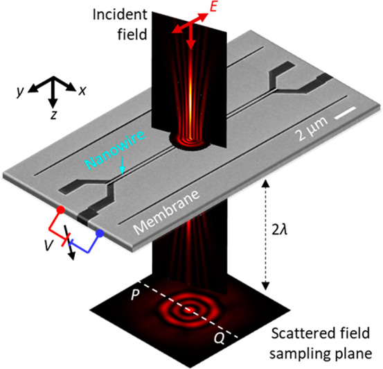
Optical metasurfaces offer a compact alternative to conventional optical elements by allowing for control over the amplitude, phase, and polarization state of light using a flat, nanostructured, surface. Single layer metasurfaces, however, preclude independent control over each of these properties with unity efficiency.86 The use of multiple metasurfaces or volume meta-optics, as presented schematically in Figure 6a, allows for far greater flexibility in manipulating the optical field while still maintaining a monolithic and compact footprint. In parallel to the fundamental advances in nanophotonics, the past decade brought numerous technological developments in nanofabrication and nanopatterning, making the researcher’s vision of the future a reality for today’s manufacturers. A typical example of a multilayer device fabricated after repeated steps of lithography is presented in Figure 6b. In this section of the roadmap, we will review some recent advances based on multilayer, multielement, and volume meta-optics and then discuss some of the current challenges, and future directions, of this rapidly advancing area.
Figure 6.
(a) A typical example of a multilayer meta-optic made of plasmonic nanoresonators separated with precise spacing using a spin-on-glass dielectric material.94 (b) 3D focused ion-beam milling of a v-shaped plasmonic metasurface stack utilized for efficient backward second harmonic generation.94 (c) Stacking metasurfaces to form a bilayer optical component, in this case, an edge imager.57 (d) Two-layer metasurfaces separated by a large distance and large energy redistribution for achieving lenses with low coma aberration.87 (e) A hybrid optical system composed of a refractive and a diffractive meta-optic designed for chromatic aberration correction.96 (f) A stack of transversely and longitudinally phase matched metasurfaces to achieve arbitrary nonlinear light manipulation capabilities.94 (a), (b), and (f) have been reproduced or adapted with permission from ref (94). Copyright 2021 APS.
6.1. Current State-of-the-Art
Multilayer meta-optics comprise two, or more, independent metasurfaces that are designed to operate as sequential optical elements. These meta-optics can be classified by the presence, or absence, of coupling between layers. In the regime where these layers are sufficiently far apart, typically a few wavelengths, each layer can serve as independent phase, amplitude, and polarization masks, greatly enhancing the design space. These masks can be fabricated separately and then combined into a bonded, monolithic, flat optics, maintaining an extremely compact footprint while offering the design flexibility of a multielement table top optical system. As an example, multiple phase masks can be used to increase the phase delay or one can combine dissimilar metasurfaces for more complex optics, such as the edge images, as shown in Figure 6c.57 In the case of the edge imager, a differentiating meta-optics was removed from the substrate and bonded with a metalens, demonstrating how dissimilar metasurfaces can be combined into monolithic thin film optics.
Spacing metasurfaces by several wavelengths, or more, allows for redistribution of light at subsequent layers, further increasing the design space. The separation between the surfaces is typically similar to the aperture size as this avoids sharp phase gradients and large diffraction angles between the surfaces. The ability to redistribute the wavefront can be used to realize wide-angle corrected lenses87 where the function of the first surface (ex. lens) is corrected, or modified, as a function of incident angle by propagation through a second surface (Figure 6d). Redistribution of the wavefront can also be used to realize loss-less full-field control where phase, amplitude, and polarization state can each be independently controlled without reflection losses.88 This is accomplished using two loss-less phase masks where the first plate serves to redistribute the wavefront at the second layer, providing a spatial amplitude profile. The desired phase function is then implemented by propagation through the second surface. Both layers can be polarization dependent enabling applications such as spatial mode division multiplexing, optical mode conversion, and universal vectorial holograms, all with diffraction efficiencies over 80%.
One can move beyond discrete metasurface optics by going to continuously structured 3D volumetric metamaterials. These systems have similar design flexibility as multilayer meta-optics but can potentially achieve that functionality in a more compact footprint. For instance, it has been demonstrated that 3D meta-optics can achieve high efficiency spectral and polarization sorting using one, continuously structured, optical component.89 This functionality is not possible in single layer metasurfaces that are invariant along the optical axis without introducing reflection loss. Recent efforts in designing various assemblies of nanostructures, distributed along the plane of the metasurfaces and disposed sufficiently close to each other to achieve nonlocal coupling effects, have enabled new phenomena and devices, including nonlocal and lattice resonance metasurfaces. In this regime of stacked layers and volumetric structures, nonlocal diffractive coupling between each layer of the stack would have to be properly considered and engineered. Nonlocal 3D meta-optics with strong out of plane coupling could potentially lead to innovative 3D collective effects and volumetric lattice resonances. Endowing each layer with a polarization control can be a particularly powerful tool. For instance, it has recently been shown how geometric, chirality-assisted, phase can be combined with propagation phase using multilayer meta-optics for independent control of two circularly polarized (CP) input beams.90 In this case, the increased design freedom associated with the metasurface stack was used to achieve distinct wavefront manipulation in all four CP output channels.
6.2. Challenges and Future Goals
Conventional refractive components generally suffer from optical aberrations, which are classified in two main categories; monochromatic and chromatic. The conventional solution to correct for the aberrations is to cascade multiple refractive optical elements along the beam trajectory. Hybrid diffractive-refractive components, as illustrated in Figure 6e, could be considered to mitigate both spherical and chromatic aberrations of the refractive optics,91−96 including cm-scale diameter lenses.92 The properties of the devices are engineered, either by relying directly on the dispersive properties of the diffractive component or by further tuning the local dispersion, finely tuning both group delay and group delay dispersion terms, of each meta-atom of the compensating metasurface.
Another challenge lies in the design of such hybrid refractive and metasurface systems. Design of modern multilens optical systems is based on ray tracing combined with powerful inverse design tools. While phase masks, representing metasurfaces, can be implemented in this process, it is much more challenging to implement metasurface libraries, especially when optimizing a design over many wavelengths. Given the bandwidth advantages of combining metasurfaces and refractive optics it is likely that work in this area will accelerate, necessitating integrated design tools for such systems.
Inverse design has become a critical tool for realizing nanophotonics and metasurfaces with increased functionality and is the subject of Section 7 of this Roadmap. The technique is equally essential for the design of multilayer systems where two, or more, layers must be simultaneously optimized to achieve a desired function. Inverse design and optimization methods appear extremely relevant in the context of multilayer systems as they help reduce the impact of reflection and diffraction losses occurring at each interface. Currently, large aperture inverse design of multilayer metasurfaces employ techniques such as angular spectrum propagation which treats each metasurface as a transmission mask. A metasurface library is typically used to find atoms that satisfy the desired transmission mask, either inside of the optimization loop, or outside of it. This is a fairly efficient design scheme that can be scaled to relatively large apertures. A challenge, however, lies in design of closely spaced, and coupled, multilayer metasurfaces as well as 3D volumetric metamaterials. Inverse design of such structures necessitates full-wave modeling of the entire aperture which currently limits the number of layers, thickness, and aperture area that can be designed. However, given the rich design space, this is an area prime for future growth if efficient simulation tools can be developed.
In addition to the linear optical properties of metasurfaces, their nonlinear optical responses have recently been studied in detail, leading to several technologically relevant photonic applications, including second-harmonic generation (SHG), photon-pair generation, all-optical switching, frequency combs, and supercontinuum generation. However, the nonlinear optical processes occurring in conventional nonlinear materials are intrinsically weak. It is extremely challenging to efficiently convert the frequency of a light beam using only a single layer metasurface, especially because the relatively poor light confinement and low Q-factor of the resonances. Additionally, the ultrathin thickness of the metasurfaces reduces the interaction length over a distance of less than a few hundred nanometers. A viable route to improve the efficiencies of nonlinear metasurfaces could consist of stacking several metasurfaces on top of each other, giving rise to designer phase-matching properties. The fundamental and application implications related to stacked or sequentially twisted metasurfaces go far beyond the simple idea of improving the nonlinear frequency conversion efficiency with phase-matched layers. Nonlinear metasurface-stacks provide entirely new capabilities that extend beyond conventional phase-matching techniques, essentially dodging the phase-matching limitation associated with the intrinsic material dispersion. The use of multilayer meta-optics could address this challenge, allowing the design of phase-matched devices along both longitudinal and transverse dimensions to exhibit arbitrary transverse field profiles. In practice, this is realized by considering the resonant phase changes of nanostructures occurring due to the coherent scattering of light at both the fundamental and the nonlinear frequency, respectively. Because these phase terms are dictated by the optical response of the nanostructures, namely, by their localized resonant oscillations, it is possible to extend a phase-matching condition to be solvable by metamaterial design. Multilayer meta-optics operating in the nonlinear regime thus provide interesting opportunities to realize nonlinear metalenses and holography.93 A phase-matched, nonlinear, multilayer meta-optics for arbitrary wavefront generation, as presented in Figure 6f, has been recently proposed.94
From a perspective point of view, the implication of phase-matched nonlinear multilayer meta-optics extend beyond simply enhancing the overall conversion efficiencies of nonlinear materials. They can tackle new fundamental and applied problems, for example, they would be used for adiabatic broadband frequency conversion in nanomaterials. This approach also becomes extremely interesting for the efficient generation of nonlinear terahertz-emitting metamaterials with designer field profiles.
Nanoimprint looks to be a promising technology for low-cost manufacturing of metasurfaces down through the visible spectrum. This technology can also be used to fabricate multilayer metasurfaces, provided they can be aligned and bonded together in a cost-effective manner. Fabrication of coupled, closely spaced multilayer metasurfaces, and 3D metamaterials is more challenging. The resolution of two-photon lithography systems, capable of 3D manufacturing, is currently close to 100 nm which should be close to the resolution needed for visible metamaterials. However, the achievable resolution is dependent on the specific geometry being patterns, and there remain challenges in translating the exposed polymer into higher index materials that are more suitable for metamaterials. The next challenge remains scalability of the approach to larger apertures, though the recent development of two-photon absorption-based patterning may offer a viable solution.95 Extending from currently available semiconductor manufacturing processes, deep-UV immersion lithography could address this challenge with a sufficient level of precision. From a research perspective, multilayer electron beam lithography (EBL) remains a suitable solution to proof-of-concept devices operating at optical wavelengths.
Stacking several active or nonlinear layers offers interesting perspectives, however, the majority of these materials are crystalline. Their assembly in a 3D structure to form a meta-crystal remains a hurdle to overcome. Additionally, thermal dissipation and structural stability of the stacks upon high intensity illumination and large changes in temperature or atmospheric conditions have to be considered for realistic applications.
6.3. Suggested Directions to Meet Goals
The realization of complex scalar and vectorial meta-optics for linear and nonlinear phase matched processes between various spatial modes opens a wide variety of applications beyond imaging, including holography and quantum computing. In order to achieve these goals, dedicated calculation tools, which can execute inverse design on large length scales and across multiple metasurfaces are needed. These tools should have the ability to properly take into consideration the diffraction of light between each layer of the stack, accounting for both propagation and resonant interaction of vectorial fields. Incorporation of refractive elements into this design architecture is essential for broadening operational bandwidth, as is needed in many imaging applications.
We expect the development of more compact, efficient, and innovative linear and nonlinear wavefront shaping devices that provide higher degrees of control, for example, operating at multiple frequencies and by featuring arbitrary intensity and polarization distributions. By stacking several polarizing elements, it is possible to release the condition of orthogonality between the polarization eigenstates of the Jones matrices, bringing the system to very peculiar responses and potentially providing flexible operations of electromagnetic waves.
Pushing the frontiers of enhanced light−matter interaction requires exploiting new concepts and innovative fabrication capabilities. For instance, multilayer meta-optics can potentially be mimicked by considering a much simpler scheme composed of a single metasurface in a cavity. In the case of multilayer architectures, new fabrication techniques are needed for both large scale patterning but also stacking and aligning multiple layers to achieve increased design flexibility. Multilayer and/or twisted metasurfaces certainly provide additional flexibility and tunability in the design of light−matter interaction, thus, contributing to the development of groundbreaking linear and nonlinear moiré physics at the nanoscale.
7. Design and Machine Learning for Metasurfaces
Jonathan A. Fan and Owen D. Miller
7.1. Introduction
Modern lithographic and additive manufacturing tools offer tremendous versatility and resolution in device patterning, enabling new classes of metasurfaces, freeform metasurfaces, that utilize hundreds of millions of geometrical degrees of freedom to achieve a desired optical response. Such devices offer new capabilities over those designed using conventional principles, including ultrahigh efficiencies, multiplexed functions (i.e., distinct optical responses as a function of wavelength, polarization, or incidence angle), and aberration correction. The extraordinary possibilities bring with it a proportionate design complexity, particularly for large area, multiscalar devices. In this section, we survey state-of-the-art techniques, open questions, and emerging approaches for freeform metasurface design that straddle the intersection of electromagnetism, optimization, and computer science. We first describe modern design techniques, including conventional concepts, adjoint-gradient methods and machine learning, and the challenges that they face, from computational scalability to practical manufacturability. We then consider the question of how to best simulate such structures, which itself presents challenges in scaling. Finally, we discuss open questions around novel applications, fundamental limits, and new design techniques.
7.2. Current State of the Art
7.2.1. Conventional and Inverse Metasurface Design
Metasurfaces are conventionally designed using a combination of physical intuition, physical approximations, and computational parameter sweeping. For local metasurfaces, in which the amplitude, phase, and polarization of an incident wavefront is locally tailored, the typical approach is to generate a library of subwavelength-scale meta-atoms comprising resonant and/or waveguiding nanoelements that collectively cover the range of desired local electromagnetic responses. Approximations, such as the enforcement of periodic boundary conditions during meta-atom simulation, are made during library generation, and basic geometric shapes are typically used. The conventional design of nonlocal metasurfaces, in which incident light couples into spatially distributed metasurface modes, starts with physical intuition to specify photonic structures supporting a dark mode, followed by structural perturbation parameter sweeping to identify layouts that support tailored mode coupling to free space. The approximations and simplifications used in these concepts ultimately place artificial design limits in device performance.
“Inverse design” methods that instead frame the design procedure as a computational optimization problem can incorporate nonintuitive wave physics and near-field coupling between nanostructures to produce devices featuring unprecedented performance and capabilities. A foundational concept in metasurface inverse design is the calculation of perturbations (i.e., gradients) to the shape or dielectric constant at all device features in a manner that improves performance. A gradient-based optimization algorithm then iteratively updates to the device layout to improve device performance. In a simple and naïve scheme for evaluating gradients everywhere in a device, individual simulations can be performed in which each device feature is perturbed and simulated. While straightforward, the number of simulations increases with the number of geometric features and is computationally intractable to perform for large area metasurfaces.
A workaround to computing gradients at all regions in a device with high computational efficiency is the “adjoint variables method” (AVM),97,98 which exploits reciprocity principles99 in electromagnetics to compute gradients at all geometric features in a device using only two simulations. Consider a metasurface, depicted in Figure 7, which is designed to function as a lens that maximizes the field at position x0 given a predetermined incident waveform, such as a normally incident planewave. First, a “forward” fullwave simulation is performed with the incident wave, from which the complex electric fields within the device and at x0 (orange point in Figure 7) are recorded. Second, an “adjoint” fullwave simulation is performed with a source located at x0 (purple double arrow in Figure 7), which has a phase opposite to that measured from the forward simulation at x0, and the complex electric fields within the device are recorded at all positions. As specified by Lorentz reciprocity, gradients (blue curve in Figure 7) at all points in the device can be computed via the product of fields from both simulations. These gradients can be iteratively utilized in standard gradient-based optimization algorithms (i.e., NLOpt, SciPy optimize, Mathworks Optimization toolbox) to produce a final high performing device layout. AVM-based metasurfaces have degrees of freedom that can exceed those in conventionally designed devices by orders of magnitude, enabling the utilization of near-field interactions between freeform-shaped nanostructures to achieve new capabilities.100,101
Figure 7.
Conceptual framework for the freeform design of a large area, multiscalar metasurface. The desired function is framed as a Figure of Merit and the metasurface layout is optimized over a series of iterations in a manner that maximizes the Figure of Merit. During each iteration, pairs of electromagnetic simulations (i.e., “forward” and “adjoint” simulations) are performed to compute gradients that specify how perturbative changes to the dielectric constant everywhere in the device can improve device performance. Algorithms (i.e., NLopt, MathWorks, scipy, GLOnet) specify the detailed utilization of gradient calculations in the optimization process.
More recently, machine-learning algorithms have emerged as candidate methods for inverse design, and they can be delineated into two classes. The first is the end-to-end training of a deep network with simulation data to learn the relationship between structure and function. The networks can then be used to perform optimization directly through backpropagation or in conjunction with a separate optimization algorithm. In the former, local gradient-based optimization is performed not in the physical metasurface design space but in an approximate surrogate neural network design space. These end-to-end models have had good success for low dimensional problems but have proven to be difficult to scale to large problems.
The second class is the training of neural networks in which iterative optimization is framed through the process of network training. One concept involves global topology optimization networks (GLOnets), which frames the population-based search for high performance devices through the training of a generative neural network.102 Over the course of iterative training, fullwave evaluations of devices are used to evolve a device distribution that starts as random to a narrow distribution of high performing freeform devices. GLOnet has been demonstrated to be particularly effective at globally searching the photonics optimization landscape and can extend to probabilistic generative networks to improve algorithm convergence. Another concept is the physics-informed neural network (PINN), in which differential equations are directly solved through network training. In these networks, the inputs are independent variables such as position, the outputs are dependent variables such as field magnitude, and the loss function contains Maxwell’s equations and the problem boundary conditions. PINNs have been tailored to directly perform refractive optics and metasurface inverse design.103
7.2.2. Simulations
A practical bottleneck to many metasurface inverse design problems is the time and computational resources required to simulate large area devices, which currently take hours to days using conventional solvers. Fortunately, significant efforts have been made to expedite fullwave simulations. One strategy has been to decompose the metasurface into modest-sized (up to ≈5 wavelengths) “overlapping domains”104 that can be independently simulated for metasurfaces with modest NA and beam-deflection requirements. Another strategy has been to parallelize conventional solvers to accelerate fullwave simulations. For example, finite-difference time domain and frequency domain algorithms have been recently adapted for use on graphical processing unit (GPU) hardware, which has led to significant speedups in the execution of these conventional solvers. Established and emergent computing methods from the computational electromagnetics community, such as the discrete dipole method, T-matrix formalisms, and integral methods, are also becoming more widely used in the photonics community and can present significant performance enhancements compared to more standard finite difference or finite element methods for certain classes of problems.
Surrogate solvers that serve as approximate Maxwell solvers have also emerged as effective high-speed simulation algorithms. Classical interpolation methods can be used to approximate electromagnetic fields associated with freeform meta-atoms given a meta-atom library reference, enabling the simulation and design of large-scale metasurfaces based on meta-atoms.105 Machine-learning tools can also serve as effective surrogate solvers that can perform fullwave electromagnetic simulations orders-of-magnitude faster than conventional algorithms. Initial fullwave surrogate simulation concepts were based on convolutional neural networks exclusively with training data, obtained using conventional simulators, to learn the relationship between nanostructure and fullwave response.106 Deep networks that also explicitly incorporated Maxwell’s equations into the loss function during training could output electromagnetic field profiles with enhanced accuracy.107 These surrogate solvers feature sufficient accuracy to be used directly in gradient-based freeform optimization algorithms and can also be utilized as preconditioners within conventional solver algorithms to expedite the computation of field solutions with hard accuracy thresholds.108 The utilization of neural networks as solvers also enables their incorporation into inverse design algorithms in new ways due to their ability to support fully analytic and differentiable relationships between structure and electromagnetic response.
7.3. Challenges, Future Goals, and Directions to Meet Goals
There remain many open research opportunities in inverse design, particularly in the topics of scalability and translation to experimental practice. While neural network-based approaches to optimization are promising, innovations are still required to push their operation to qualitatively new regimes of device scale and computing efficiency. For example, PINNs currently take longer to train than conventional differential equation solvers, and it remains unclear how effectively GLOnet can optimize very large-scale problems. In both cases, insights and innovations in network architecture and training procedure, including automated selection of architectures, will be required. There is also the open question of how to ensure that optimized freeform devices are robust and capable of being reliably fabricated. Various concepts have been developed to help specify the incorporation of minimum feature sizes109 and insensitivity to global geometric perturbations, but more advanced sensitivity analysis and robustness criteria are still required, particularly for volumetric metasurfaces and devices featuring high quality factors. One interesting new avenue110,111 is the rewriting of the Maxwell design problem as a “quadratically constrained quadratic program” that offers the possibility for circumventing local optima by moving to a high-dimensional space and using convex-optimization techniques.
There are also significant opportunities to further enhance the speed and accuracy of electromagnetic solvers. Many of these opportunities will be catalyzed by continued interactions with the computational electromagnetics community, which has been in the business of innovating new fullwave simulators for large-scale systems. These innovations will be both on the algorithm side and in interfacing with new hardware that can accelerate simulations through enhanced parallelization, in-memory computing, and operation-specific computing. On the deep-learning front, new and emergent concepts in neural network architectures, such as graphical neural networks, will enable more efficient descriptions of structures and electromagnetic fields. Significant work is also required to adapt neural network surrogate solvers to problems with arbitrary domain sizes and adaptive spatial resolutions. On the training data front, many surrogate solver concepts rely on the production of simulated data with very specific domain sizes and resolution, which is computationally costly. New concepts that can enable more generalized use of simulated data for network training would break through this training data bottleneck problem. The use and sharing of data sets112 will also be important for the broad acceptance and usage of data science approaches.
7.4. Applications
The development of high-speed, high-performance inverse design algorithms will enable new classes of metasurface technologies with unprecedented efficiencies, capabilities, and form factors. We anticipate that these new design platforms will enable the realization of large-area, centimeter-scale metasurfaces, which can serve in imaging and display systems as aberration-corrected imaging optics and waveguide couplers for AR/VR (augmented reality/virtual reality) systems. They also can serve as new classes of nonlocal and narrowband devices, which blur the lines between integrated and freespace optics and require large areas to support high quality factors. Applications include sensing, nonlinear transduction, optical computing, and active metasurface control. The high efficiencies supported by freeform design will further enable the practical use of metasurfaces in the quantum information sciences, in devices spanning optical atom traps to polarization state generators and analyzers. We also anticipate that new imaging capabilities will be supported by multifunctional metasurfaces designed in conjunction with computational imaging algorithms.
The technological capabilities and commercial potential of freeform metasurfaces will continue to increase as manufacturing methods advance. These include the fabrication of multilayer dielectric structures with foundry-compatible nanofabrication process, the additive manufacturing of volumetric, high-dielectric-contrast structures at the nanoscale, and the utilization of new materials with unusual optical properties. Proof-of-concept demonstrations of multilayer devices at optical wavelengths and volumetric devices at radio frequencies indicate that the addition of such degrees of freedom can enable metasurfaces with qualitatively new capabilities, as described in Section 6. As such, it will be important to ensure that continued developments in optimization and simulation algorithms are adaptable to new classes of materials and volumetric metasurfaces form factors. The maturity of manufacturing methods for active and passive devices at radio wave and millimeter wave- lengths also points to more immediate opportunities to develop and apply inverse design methods to technologies operating at these frequencies.
8. Computational Imaging with Meta-Optics
Arka Majumdar, Johannes E. Fröch, David Brady, Felix Heide, and Ashok Veeraraghavan
8.1. Introduction
With the rapid advent of the Internet of Things (IoT) and autonomous systems, there is an urgent need for compact, low power, ubiquitous image sensors to bridge the gap between the physical and the digital world. Current image sensors, however, often entail bulky elements incapable of meeting the demand for next-generation imaging systems. Computational imaging reduces this complexity by replacing sophisticated optics with simple elements and leverages computation to transfer part of the imaging process to software. However, the power consumption in these computational reconstruction algorithms is often prohibitively large. Additionally, many sensing applications require only parts of a scene for decision-making, in which case, high-resolution imaging followed by digital feature extraction is excessive and unnecessary. Finally, many machine vision applications need more than just 2D intensity information, typically captured by traditional cameras. Extracting this information, including depth, and spectra requires significant computation. One promising solution could be to perform some image processing directly in the optical domain, and thus balance the computational burden between the optics and software. Such optical image processing is passive, and moreover, the processing happens within a very short time, minimally affecting the latency. However, analog optical information processing has been plagued with numerous problems in the past, including large size and stringent requirements on alignment. In recent years, macroscopic freeform optics have demonstrated the possibility of combining the functionality of multiple optics into fewer elements, and thus can potentially be used to create such optical information processing systems. Unfortunately, these computational elements often entail complicated geometries, and fabricating them becomes painstakingly difficult.
In recent years, advancements in microfabrication and nanophotonics have given rise to meta-optics, enabling drastic miniaturization of optics by using quasi-periodic arrays of subwavelength scatterers to modify incident electromagnetic radiation. These meta-optics enable fabrication of freeform surfaces using single stage lithography. Additionally, each scatterer in a meta-optic can be independently tailored to modify the amplitude, phase, and polarization of wavefronts. In fact, several research groups have already demonstrated various meta-optical elements, including lenses, wave-plates, polarization and spectral filters, and holograms. Thus, the combination of optical image processing with meta-optics and subsequent computational imaging in software presents a tremendous opportunity to design next-generation sensors for applications in IoT and machine vision (Figure 8). In this Roadmap, we will review the current state of meta-optical computational imaging and outline several challenges and research opportunities in this field. We will primarily focus on visible and near-infrared wavelengths in this article, although similar computational imaging has also been explored in the microwave domain.113
Figure 8.
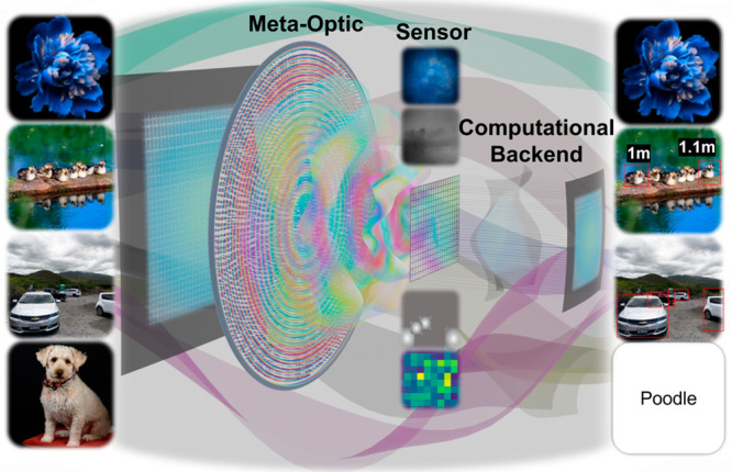
By optimizing meta-optics, along with a computational backend, a dramatic reduction in size, weight, power, and latency of image sensors can be achieved. Here, we consider four examples, where the objects are shown in the left and desired sensing output is shown in the left. We envision the computational sensors can either capture aesthetically pleasing images (row 1), or capture additional information from the scene, such as depth (row 2) or spectrum. We envision that some of these can even perform computation for object detection (row 3) or scene understanding (row 4).
8.2. Current State of the Art
Computational imaging was first used in conjunction with an extended depth of focus (EDOF) cubic meta-optics for full color visible imaging.114 Along with intuitive designs, researchers employed inverse designs to create EDOF meta-optics,115 which along with computational imaging demonstrated broadband imaging. The image quality improved substantially, when an end-to-end design was used to co-optimize the meta-optics with a computational backend.116 Along with full-color imaging, meta-optical computational imaging techniques have been used for depth sensing, using depth from defocus117 or exploiting the inherent chromatic aberration of meta-optics,118 varifocal imaging119 and spectroscopy.120 Meta-lenslet arrays have also been used along with computational imaging for lightfield imaging.121 A meta-optical front end can encode information from a scene, which in conjunction with a computational backend can perform object detection.122
8.3. Challenges and Future Goals
In spite of impressive demonstrations, the performance of meta-optical computational imaging systems is far from the desired performance. For example, the images captured with meta-optics have remained inferior in quality to images taken with refractive lenses. Additionally, while various properties of light, including polarization, orbital angular momentum, or spectrum, have been exploited in pure meta-optical imaging or holography, the combination of computational imaging and multimodal imaging via meta-optics has not yet been exploited. Along with these extensions to already existing works, we outline several future directions where meta-optics can play an important role for computational imaging.
8.4. Suggested Directions to Meet Goals
8.4.1. Synthetic Aperture Imaging
Conventional lens-based imaging systems face stringent trade-offs between light throughput, resolution, depth-of-field, and size (volume/weight) primarily because all of these variables are fundamentally directly related to the diameter of the lens. Synthetic aperture imaging provides a way to break away from these constraints by using a collection of subapertures. This approach has yielded amazing results in radar and mm-wave, including the recently released first image of a black hole through this approach. In light-based imaging (visible, infrared or even thermal), these techniques have had so far minimal impact, because precise alignment and calibration between multiple refractive multielement systems that are not axis-aligned are challenging and the higher optical frequency implies that phase cannot be directly measured at the detector. However, emerging advances in meta-optics and computational algorithms have the potential to dramatically alter the state of art in this space.
First, meta-optics being two-dimensional and lightweight, upend the current cubic relationship between aperture diameter and weight. Second, the two-dimensionality of these meta-optics provide scalable opportunities for precise alignment allowing us to compose ever larger composite apertures that may be made of a sparse array of smaller metasurfaces. Third, advances made over the past decade in phase retrieval-based algorithms allow us the opportunity to use algorithms to computationally retrieve phase information from amplitude measurements. Finally, the rapid advances in machine learning, especially end-to-end learning systems that can co-optimize for the aperture functions and the reconstruction algorithms allow us to capitalize on the new degrees of freedom afforded by meta-optics.
Over the past few years, several approaches have emerged that utilize these newfound degrees of freedom to realize synthetic aperture imaging within optical imaging.123,124 We believe that these approaches are only beginning to scratch the surface of what is possible and that codesign of meta-optics along with associated machine learning reconstruction algorithms provide us with the opportunity to leverage synthetic aperture techniques and reach parts of the aperture size, weight, resolution, light-efficiency tradeoff space that have previously not been explored.
8.4.2. Fourier Ptychography
Meta-optics are immediately attractive for computational imaging with coherent illumination. Coherent imaging systems are spectrally narrow-band and inherently computational. Hence, the spectral sensitivity and diffractive artifacts of simple meta-optics are useful features rather than challenges. The role of optics in coherent systems is to phase-code wavefronts for subsequent computational reconstruction. Conventionally, this is performed with holographic reference signals, but as computational power and physical coding methods have improved, reference-free phase retrieval strategies have become increasingly attractive. Fourier ptychography (FP) is a phase retrieval system that exploits phase diversity from light coming from different angles via structured illumination or multiaperture imaging, to reconstruct wavefronts.125 FP most commonly uses sequences of illumination patterns or object-target motion to capture phase-coded images. Recent preliminary studies have shown that diffractive elements may be used to code image patterns for a single snapshot imaging. Thanks to the large space-bandwidth product, meta-optics increase the coding capacity and efficiency of such elements. Design of these elements is a classic computational imaging challenge: meta-optics must match the natural sampling period posed by the pixel-pitch of the sensor to the object field and must simplify the computational load. Interleaved meta-lenses can potentially enable compact, high-resolution imaging for remote fields. The angular spread of the light from a remote object plane is generally low, i.e., the field has a low NA. FP imaging typically requires 4−16× oversampling, meaning to reconstruct the complex field (both amplitude and phase) of a single point in the object plane, 4−16 sensor pixels (capturing only intensity value) in the image plane are needed.126 By mapping such low NA incident field from the object to high NA oversampled images, meta-optics enables a novel wavefront sensitive image plane with relatively simple computational load.
8.4.3. High Dynamic Range Imaging
High-dynamic range (HDR) imaging is an essential imaging modality for a wide range of applications in uncontrolled environments, including autonomous driving, robotics, and mobile phone cameras. Existing HDR sensing approaches struggle with dynamic scenes due to multishot acquisition and postprocessing time, e.g., mobile phone burst photography, making such approaches unsuitable for real-time applications. In particular, computer vision in outdoor scenarios at real-time requires accurate and robust HDR reconstruction, with safety-critical applications from self-driving vehicles and advanced driver assistance systems to drones and robots in farming and outdoor maintenance. Challenging in-the-wild scenarios include facing the sun in the presence of large, shadow-casting objects or moving from indoor to outdoor and back, e.g., entrance and exit of a tunnel. In such cases, the range of luminance seen at the same time can reach ∼180 dB, exceeding the range of today’s robotic and automotive image sensors that covers around ∼120−140 dB. These existing sensors already employ complex split-pixel and multiexposure sensing schemes that make use of both temporal and spatial multiplexing for sensing these extreme dynamic ranges on a given sensor. An underexplored avenue lies in the optical encoding of HDR information and learning an optical HDR encoding map with saturated highlights into neighboring unsaturated areas. While existing work has shown promising first results that such optical encoding with a single fixed element may allow for effective HDR recovery,127 a joint design with the sensor and potentially reconfigurable metasurface offers exciting potentials for HDR imaging. Such a joint design could not only adaptively distribute intensity over the sensor to different pixel architectures best tailored to the intensity, but also allow us to rethink the array sensing by itself. This new breed of computational meta-optical HDR cameras may be capable of redistributing light not only based on intensity but also polarization, wavelength, and angle. It may also allow for a simplified sensor design where different pixel and read-out circuit architectures could support a lower dynamic range in conjunction with optical multiplexing.
8.4.4. Hyperspectral Imaging
The spectral information of scenes can hold invaluable information beyond hue, saturation, and brightness. Hyperspectral imaging is a concept where the captured scene is presented by a data cube with each pixel of the scene containing a full spectrum. This information can unveil properties that are otherwise hidden in the broad spectral response of imaging sensors, such as Bayer filters for full color imaging in the visible. Hyperspectral imaging already finds use for a plethora of applications covering industry, military, or medical research. For instance, remote sensing with drones/ satellites can be used to monitor the quality of agricultural fields, or cancerous tissue can be accurately detected using their distinct spectral signatures. Beyond that, consumer electronics, such as smartphones, could greatly benefit from such systems for personal health or food monitoring.
Current solutions for this modality are, however, either inefficient, bulky, or rely on scanning elements, often prohibiting their integration into mobile devices, limiting their speed and thus their deployment. Therefore, a common challenge is to find solutions with smaller device footprints, no moving parts, and lower power consumption. Meta-optics may be particularly well suited to solve this challenge due to their reduction in size and weight over traditional refractive elements. Moreover, these subwavelength diffractive elements typically have a strong chromatic response. While previous works aimed to eliminate their aberrations by designing meta-optic doublets, engineering the scatterer dispersion, or a computational reconstruction, future works could be directed toward exploiting this feature. For that, ideally an end-to-end design approach will be utilized, where the meta-optic is co-optimized with a computational backend. While the hardware will encode the spectral information into a specific local intensity distribution through the chromatic point spread function of the meta-optic, the computational backend in this case is co-optimized to efficiently retrieve the pixel-by-pixel spectral information.
8.5. Relevance to Industry
While many of these research directions need fundamental innovation and potentially will guide many new academic research directions, there is a strong industrial relevance of meta-optical computational imaging. Computational imaging is already prevalent in industry, for example, almost all mobile photography currently uses computational amelioration of the captured images. Additionally, meta-optics also have generated strong commercial interest, with several startups and large companies trying to commercialize meta-optics, with applications in mobile photography, sensing and biomedical imaging. Several foundries have also started manufacturing meta-optics in high volume using immersion and nanoimprint lithography. Thus, combination of meta-optics and computational imaging is in an opportune place to be adopted by industry. Especially, making ultracompact imagers, either for full-color imaging or for simultaneous localization and mapping in wearable devices and time-of-flight sensing have strong commercial interests. Additionally, for biomedical imaging and endoscopy, there is a constant need for miniaturization, where meta-optics can play an important role.
9. Optical Computing with Metasurfaces
Nader Engheta, Andrea Alú, and Albert Polman
9.1. Introduction
Light−matter interaction is one of the fundamental phenomena in the fields of electrodynamics and materials science. Since optical signals propagate with ultrahigh speeds, one may wonder whether light can be exploited for performing ultrafast, low-power computation and mathematical operations, particularly at the nanoscale. In other words, can we envision “nanoscale light machines” for “doing mathematics with light” or “solving equations with light” as the light wave interacts with properly designed collections of nanostructures? Since the development of science and technology largely relies on handling, processing, and performing mathematical operations on large amounts of data, exploring new paradigms for fast and low-power processing of such data is of growing importance in our data-driven world. Nanoscale optics and optical metasurfaces may bring transformative solutions into this arena.
9.2. Current State of the Art
Optical signal processing is a well-established field, particularly in the field of Fourier optics in which signal processing is primarily achieved with Fourier transformation using light interaction with lenses. Conventional Fourier optic platforms require bulky setups and careful alignment of several optical devices, with limited flexibility and hindering the overall applicability of these powerful tools in nanophotonic settings. While optical analog computing has recently been resurrected as an interesting platform for computation,128,129 and collections of photonic processors, such as meshes of Mach−Zehnder interferometers [MZIs], have been proposed as a programmable photonic platform for linear optics,130,131 the field of metamaterials and metasurfaces has recently offered an entirely new mindset for analog computation using light.132,133 Since optical waves can be tailored by materials, judiciously engineered material structures such as metasurfaces can be utilized to manipulate waves in order to achieve useful functionalities for computation and signal processing, over dramatically reduced footprints and with much more flexible implementations. As a representative example, Figure 9a presents the sketch of the idea of a metasurface that can perform arbitrary mathematical operations.133 Specifically, one can design metastructures such that when a monochromatic wave with an arbitrary spatial profile enters this metastructure, the profile of the output signal resembles the desired mathematical (linear) operation on the input profile. The examples of linear operators discussed in ref (133) include first-order and second-order (spatial) differentiation, spatial integration, and spatial convolution. In particular, the operation of second-order derivative is of special importance in the field of image processing and pattern recognition, as it reveals the edges of an image (Figure 9b). The analog nature and parallelism of such analog edge detection in image processing offers possibilities for high-speed operation, with no raster scanning. In other words, the entire image can be processed at the same time, providing ultrafast low-power processing. This potential application was numerically demonstrated in ref (133), as shown in Figure 9b. Engineered nonlocalities in metasurfaces exploiting Fano resonances have been shown to form a flexible tool for this goal, achieving first-order and second-order differentiation134 (see Figure 9c), and the experimental verification of second-order differentation and image edge detection using metasurfaces made of Si nanobeams on Al2O3 (Figure 9d) have been subsequently demonstrated135 (Figure 9e). Other exciting theoretical and experimental demonstrations of metasurfaces with the differentiation capabilities have also been reported.57,136
Figure 9.

Metasurfaces for optical computing and signal processing: (a) Sketch of the idea of metasurface that can perform mathematical operation on the profile of the incoming wave. Reprinted with permission from ref (133). Copyright 2014 AAAS. (b) Numerical demonstration of edge detection using the metasurface designed to perfrom the second-order spatial differentiation. Reprinted with permission from ref (133). Copyright 2014 AAAS. (c) Nonlocal metasurface using an array of split-ring resonator. Reprinted with permission from ref (134). Copyright 2018 American Physical Society. (d) the scanning electron mictroscopy (SEM) image of the Si metasurface performing second-order spatial differentiation, Reprinted from ref (135). Creative Common License, Copyright 2019 American Chemical Society. (e) Experimental second-order image differentiation using the structure shown in (d). Reprinted from ref (135). Creative Common License, Copyright 2019 American Chemical Society. (f) Sketch of the idea of inverse-designed metastructure with the feedback for solving integral equations, Reprinted with permission from ref (137). Copyright 2019 AAAS. (g) The specific metastructure designed for experimental verification for integral equation solving. Reprinted with permission from ref (137). Copyright 2019 AAAS. (h) The photograph of the structure. Reprinted with permission from ref (137). Copyright 2019 AAAS. (i) From ref (138): Schematic on integral-solving metasurface geometry and scanning electron microscopy (SEM) image of an inverse-designed Si metagrating for equation solving with free-space visible radiation. Reprinted with permission from ref (138). Copyright 2023 Springer Nature.
Remarkably, metasurfaces can also offer the possibility of solving equations using electromagnetic waves.137 To realize such possibilities, in ref (137) the general class of linear integral equations, i.e., the Fredholm integral equation of second kind, g(y) = Iin(y) + ∫baK(y, y′)g(y′)dy′, was considered. In such scenarios, the metasurface can be designed using inverse design methods, to represent the generally nonseparable, shift-variant kernel K(y,y′) (Figure 9f). In order to endow this metasurface with equation solving capability, one needs to add a feedback loop to the system, i.e., the output of the metasurface should be fed back to its input. This feedback allows the Neumann series to be performed at the speed of light (Figure 9f). The input Iin(y) can be entered into the system using directional couplers and the output of the system, which represents the solution of the integral equation, g(y), can also be read out using directional couplers. Figure 9g,h shows such inverse-designed metastructure built and tested in the microwave regime, demonstrating the ability of this structure to solve the integral equations. Recently, optical metasurfaces, in the form of inverse-designed Si-based metagrating, have been constructed and experimentally verified, showing equation solving capability for free space visible radiation using a compact planarized metasurface platform138 (see Figure 9i). Even a single cylindrical nanostructure, designed using the inverse design method, has been proposed for integral equation solving following a similar strategy.139 In this scenario, the inputs are mapped into the incoming wavefront, exciting the scatterer from the far-field, and the solution of the mathematical problem can be read in the scattered wavefront.
Since photons do not interact with each other in linear media, all these analog optical computing metasurfaces provide exciting possibilities for low-power, near-speed-of-light, parallel signal processing. This aspect was examined in ref (140), in which it was demonstrated, numerically and experimentally in the microwave regime, that a single inverse-designed metastructure can solve more than one equation simultaneously, when electromagnetic waves travel through this structure. Specifically, the experimental setup was designed to solve two integral equations with two different kernels K1(y,y′) and K2(y,y′), with arbitrary inputs I1(y) and I2(y). To achieve this, a single metasurface was designed and constructed such that for the operating frequencies ω1 and ω2, the metasurface functions as kernels K1(y,y′) and K2(y,y′), respectively. In ref (140), it has also been shown, through numerical simulations, that one can design a metasurface that can invert four different 5 × 5 matrices, when it is being operated with four different frequencies.
9.3. Challenges and Future Goals
While metasurface-based analog optical computing provides an exciting platform for computation and information processing, there are challenges and limitations in its operation as of today. Examples, aside from fabrication imperfections, are noise accumulation in cascading such systems, limited reconfigurability, and lack of direct photon storage, as well as limitations in the type of mathematical operations and processing that is available. Several current research directions are being explored to address these limitations. For reprogrammability of these analog meta-matchines, the use of reconfigurable Mach−Zehnder interferometer (MZI) meshes130,141 and phase-change materials142 have been proposed and are being investigated. Recently, using reconfigurable couplers (such as MZIs and Direct Complex Matrix (DCM) architectures) it has been shown theoretically that linear differential and integral equations can be solved.141 The experimental verification of such programmable computing machine has also been achieved recently. Moreover, the combination of inverse-designed metastructures with reconfigurable couplers has also been explored and studied for forward scattering problems. For photon storage and memory, nonlinearities may be employed, as recently investigated in combination with bound-states in the continuum. Nonlinearities may also help broaden the reach of these meta-structures, which are now limited to linear operations. By tailoring optical nonlinearities, it may be possible to realize complex nonlinear analog computations, largely broadening the reach of this field of research, with applications that extend to the fields of cryptography, deep learning and quantum computing.
In conclusion, analog optical computing with metasurfaces offers integrable, low-power, ultrafast meta-machines that promise significant impacts in various fields of science and engineering with high demands for data and information processing.
10. Tunable Metasurfaces: Opportunities and Needs
Harry A. Atwater, Prachi Thureja, and Ramon Paniagua-Dominguez
10.1. Current State of the Art
With an expected size exceeding a trillion U.S. dollars by 2025, the global photonics market is quickly expanding, due to the continuous growth of established areas, such as smart lighting and displays, as well as new optical technologies for sensing and spectroscopy, 3D mapping and ranging (including LiDAR), holography, and optical communications to name a few. Common technology trends identified in all these areas are the need for device miniaturization, improved performance, novel multifunctional components, and deeper integration with electronics. Optical phased arrays have previously been demonstrated as a first generation of beam steering apertures. However, the sparse arrangement of waveguides for reduced crosstalk inhibits the realization of two-dimensional wavefront control with a wide field-of-view.
Metasurfaces offer tremendous opportunities, as they allow manipulation of the amplitude, phase, and polarization of electromagnetic waves with arrays of subwavelength nanoantennas,1 enabling systems with flat optical components featuring dramatically reduced size, weight, power, and potentially cost. Currently, however, most metasurfaces are “static” and have functions that are fixed at the time of fabrication. By making the system reconfigurable in its phase, amplitude, and polarization response through incorporation of a tuning mechanism, one can achieve real-time control of the optical function and even access multifunctional characteristics postfabrication. This has triggered intensive research in the field of active metasurfaces,143,144 with different tuning mechanisms and device architectures being explored.
In very broad terms, one can first classify active metasurfaces based on the attainable degree of spatial and temporal control. The spatial degree of freedom spans from devices that can be reconfigured as a whole, from the simplest case of on−off switching to continuous tuning of an optical function such as varifocal lensing, to those in which each individual nanoantenna in an array can be addressed individually. The degree of temporal control is connected to the reconfiguration time scale: In quasistatic metasurfaces, temporal variations are slower than the period of electromagnetic waves, while time-modulated structures are those that are modulated fast enough to alter the frequency of the incoming beam.
Quasistatic Metasurfaces vs High-Frequency, Time-Modulated Metasurfaces
Like today’s static metasurfaces, quasistatic and high-frequency, time-modulated metasurfaces are chip-based low-profile structures with compact footprints, featuring an ultrathin thickness, and a flat macroscopic geometry, allowing these platforms to replace a variety of bulky passive and active optical components for both spatial and temporal optical modulation. Furthermore, the subwavelength dimensions of resonant unit cells substantially reduce the power requirements for high-frequency, temporal modulation of light compared to bulky modulators having large half-wave voltages.
Quasistatic modulation refers to the regime in which temporal variations are slow enough that they do not change the scattered beam frequency. Metasurfaces operated in this regime instead allow dynamic control over the amplitude, phase, and polarization of an electromagnetic wave. Thus, they generally enable versatile wavefront shaping by tailoring the scattered phase profile to achieve, e.g., beam steering, focusing, switchable diffractive or holographic elements, or special beam profiles including “flat-top” angular beam profiles, complex beams carrying orbital or spin angular momentum, or nondiffractive beam profiles for the intermediate field.
Time-modulated metasurfaces are those that introduce a change in the scattered beam frequency by modulating the properties of light, particularly the phase, at high frequencies.145 For practical use, the modulation frequency should be large enough, so that the generated frequency harmonics can be distinguished from the incident laser frequency. As such, modulation frequencies larger than the line width of the incident laser are needed (i.e., ≳50 kHz). These devices are interesting because they enable novel functions that are not attainable with their quasistatic counterparts. For example, when considering steered optical beams, functionalities like those achievable at radio frequencies (RF) become available.146,147 These include nearly dispersion-less and broadband sideband beam steering, frequency multiplexing, frequency selective switching, multichannel and full-duplex operation, as well as Doppler-enabled effects. They also provide unique opportunities for color-shifting devices (potentially in reflection, transmission, and diffraction), to realize nonreciprocal devices like optical isolators and circulators, frequency transformations via temporal discontinuities and other sorts of spatiotemporal light manipulation. One can envision, for example, that a scattered incident optical beam at a single frequency could be dispersed over a range of scattered frequencies to “spectrally camouflage” an object.
10.2. Challenges and Future Goals
Materials Considerations
Beyond the classification of active metasurfaces in terms of their degree of spatial and temporal control, one can further differentiate metasurfaces based on which properties of light they manipulate and whether those properties are controlled in reflection or transmission, as illustrated in Figure 10 (left). The physical modulation mechanism and the corresponding material choices (Figure 10, right) furthermore define its characteristics, such as the wavelength of operation, volatility/nonvolatility, cyclability and device lifetime, modulation depth, etc., and its use cases.
Figure 10.

Active metasurface configurations (left) and physical mechanisms for modulation (right).
Arguably, a universally reconfigurable metasurface would provide full and independent control over the amplitude, phase, and polarization of light at the single nanoantenna level and additionally allow high-frequency manipulation, if so desired. Moreover, for it to be useful, it should do so in an efficient (in terms of photons out per photons in) and practical fashion (ideally addressed by electrical signals due to their robustness and compatibility with modern integrated circuits). With this in mind, a few tuning mechanisms, in particular, those based on electro-optical or electro-thermo-optical effects, seem promising to satisfy all, or at least most, of these requirements. In the following, we briefly summarize the opportunities and challenges that they present.
Liquid Crystal Reorientation
Liquid crystals (LCs) are a well-established material platform for dynamic light modulation. They are present in many commercial devices that serve this purpose, such as Spatial Light Modulators using CMOS backplanes (so-called Liquid Crystal on Silicon, LCoS). These devices use the natural birefringence of LCs to modulate the phase, amplitude, or polarization of light upon propagation through an LC layer. Their combination with resonant nanoantennas offers venues for pixel miniaturization compared to LCoS modulators, while still being able to take advantage of their mature manufacturing and processing technologies. However, reaching submicron scales without incurring interpixel crosstalk is still an open challenge. Owing to the large and continuous index modulation of LCs with an external bias (Δn ∼ 0.2 being easily attainable), they allow large modulation depths without the need for sophisticated nanoantenna designs.148,149 Moreover, due to their high transparency at visible frequencies, LC-based tunable metasurfaces are particularly promising to realize high-efficiency devices in this frequency range, rendering these structures particularly suitable for holographic imaging and optical sensing. The main disadvantage of this approach is the limited response time of LCs, on the order of hundreds of microseconds to milliseconds, which poses a severe limitation for their application in high-frequency beam manipulation for optical communication and neuromorphic photonics.
(Electro-) Thermo-Optical Effects
Micro- and nanoheaters can be used to locally modify the temperature of the nanoantennas or their surroundings using electrical currents and, in turn, their resonant frequency. This can be due to thermo-optical effects150 or, in some cases, a change in the material crystal structure via phase change. While the former effect is typically weak, the latter can lead to drastic changes in the refractive index (Δn ∼ 1) across the visible and infrared spectrum, easing the optical resonator design.151 The nonvolatile nature of several phase change materials further reduces power consumption. MHz modulation frequencies should be achievable with thermo-optical and phase change effects, provided good thermal management is incorporated in the device design. Subwavelength unit cell control, particularly in 2D architectures, requires careful design of thermo-optically controlled metasurfaces to mitigate crosstalk effects. Additional challenges in terms of cyclability and device lifetime might emerge when modulating phase change materials at high frequencies. The characteristic properties of thermo-optically modulated materials make them ideally suited for use in dynamically reconfigurable displays and memristive devices.
TCO/Free Carrier Index Modulation
Among the different electro-optical tuning mechanisms, those relying on free-carrier effects in transparent conducting oxides and semiconductors are of particular interest for the realization of universally reconfigurable time-modulated metasurfaces due to the short response times (potentially reaching down to nanoseconds), compact design, and lower power consumption. These mechanisms include field-effect modulation of carriers in parallel capacitor configurations, double carrier injection in p−i−n semiconductor junctions, and carrier accumulation/depletion in p−n junctions. A proper electrical and photonic design of the constituent unit cells is required to maximize the dynamic range of tuning for scattered light phase and amplitude, while maximizing the interaction strength of light with the active material regions.152 Plasmonic resonators and cavities are often employed to achieve the required high field confinement; however, this in turn contributes to high absorption and therefore lower power efficiencies. The operating wavelength of metasurfaces relying on free-carrier index modulation is determined based on the choice of the active material and its doping. Most demonstrations to date have thus relied on operation in the near- to far-infrared spectrum. Emerging materials for operation in the visible include transition metal nitrides153 and transition metal dichalcogenides.154
Electro-Optic Effect (Quantum Confined Stark Effect, Pockels Effect)
The quantum-confined Stark effect in III−V multiple-quantum well (MQW) structures is an ultrafast electro-optic (EO) effect which can be used for achieving gigahertz modulation and realizing high-efficiency, all-dielectric metasurfaces. While MQW structures have been proposed to realize active metasurfaces in the near- and mid-infrared,155,156 advances in the fabrication of thin films of electro-optic crystals, including lithium niobate and barium titanate,157,158 have recently propelled the use of electro-optic tuning via Pockels effect for broadband modulation across the visible and infrared. The refractive index change introduced through the Stark or Pockels effect is typically small although it can be achieved over a large volume. As a result, there is a tradeoff between the resonance mode volume and its quality factor in order to enhance the dynamic range for phase modulation and the amplitude modulation depth. The volume for field confinement in the active dielectric unit cell determines the effective antenna size, while the quality factor determines the phase modulation range, with narrower resonances leading to larger phase modulations. Nonlocal metasurfaces,159 including metasurfaces governed by guided mode resonances (GMRs) or optical bound states in the continuum (BIC) and quasi-BICs, have emerged as a potential pathway for the realization of high quality active metasurfaces. However, further studies are needed to develop design principles that enable efficient and versatile wavefront shaping on an array level using nonlocal metasurfaces. It might be worth mentioning here as well EO polymers, which make use of the Pockels effect for modulation. Largely explored in integrated photonics, their use in the field of metasurfaces is still limited, mainly restricted to devices operating in the GHz range. While they can offer high modulation frequencies, they might come with additional challenges, such as photodegradation.
Architectural Considerations
To date, most experimental realizations of active nanoantenna arrays with individual pixel control have been restricted to demonstrations of beam steering and wavefront shaping along one spatial dimension. Extending active metasurface apertures to two dimensions is more challenging owing to the required addressability of each pixel in the array. Such devices, however, would substantially expand the degree of light manipulation, allowing for more versatile optical functions. The major challenge toward the realization of two-dimensional active metasurfaces is the design complexity of the interconnect structure which substantially increases from one to two dimensions. Scaling of active metasurfaces to large areas additionally requires compact footprint interconnect designs.
Although both reflectarray and transmittarray configurations are of interest depending on the application, each presents its own opportunities and challenges. On the one hand, transmitarrays would notably enable integration of active metasurfaces to form complex systems that allow for cascading of multiple active metasurface planes as well as easier integration with laser and LED light sources or focal plane array detectors. Their compact footprint could also open exciting opportunities for monolithic integration into on-chip laser systems to realize compact metasurface-based optical sources with complex functions. While realizing designs for tunable transmissive metasurfaces with continuous 2π phase modulation and high transmission intensity forms its own challenges, additional difficulties occur when developing suitable architectures for individual pixel control with minimal optical interaction between the incident electromagnetic field and the interconnects. Reflectarrays, on the other hand, might benefit from using CMOS backplanes and their advanced integrated circuit architectures with which the individual addressing of millions or tens of millions of pixels at the wavelength scale would seem feasible. On the downside, their integration in complex optical systems, such as cascaded metasurfaces or a combination with integrated light sources, is less straightforward than in the case of transmitarrays. An additional point to be considered is that transistors can only supply a relatively small (∼1 V) dynamic voltage range when working with small technology CMOS nodes (e.g., 40 nm). Thus, when using these architectures, one should ensure that all the required light modulation can be achieved within this bias range.
10.3. Suggested Directions to Meet Goals: Toward Universally Tunable Metasurfaces
Substantial research on active metasurfaces has led to the emergence of a new generation of optical elements enabling dynamic and deterministic control over light. Electrical biasing of metasurface unit cells in particular has established itself as a practical approach for precise wavefront engineering at the subwavelength scale. In this realm, several modulation mechanisms, including those based on liquid crystals, thermo-optic effects, field-effect carrier modulation, as well as electro-optic tuning have been proposed. Liquid crystal-based metasurfaces and those based on phase-change materials stand out in terms of the large index changes across the visible and infrared spectrum. However, liquid crystal-based structures lack in their response time, while the main limitation of phase change materials is the repeatability over large number of cycles as well as high power consumption in volatile materials. In addition, both approaches are limited in their field-of-view due to crosstalk effects. Field-effect tuning based on carrier modulation is a promising approach for high-frequency modulation that allows strong confinement of resonant modes to subwavelength unit cells through appropriate design of plasmonic resonators and cavities, however, this localization comes at the cost of power efficiency. While metasurfaces based on electro-optic tuning offer an alternative approach for low-loss modulation schemes, larger quality factor structures (that often come at the cost of larger pixel sizes) are required to achieve substantial phase modulations. Lower quality factor designs could potentially result in high-performing devices with large applied voltages. However, this complicates the realization of two-dimensional arrays with submicron unit cells, which must rely on small supply voltages. Thus, additional efforts in the realms of materials and device design will play a crucial role over the coming years to enable efficient and versatile metasurfaces for quasi-static and time-modulated operation. On a system level, the design of new interconnect architectures that minimally interfere with the optical response of metasurfaces operating either in transmission or reflection are needed to move toward full two-dimensional beam shaping. Advances in computational design algorithms will further enhance performance of active metasurfaces in various technologically relevant applications, encompassing fields from optical imaging and quantum sensing to optical computing and communication.
11. Active Light-Emitting and Light-Trapping Metasurfaces
Son Tung Ha, Angela I. Barreda, Albert Polman, Jon A. Schuller, and Isabelle Staude
11.1. Current State of the Art
Metasurfaces have been vastly investigated in the recent years as promising structures for controlling light emission at the nanoscale. Light-emitting metasurfaces can be realized by integrating nanoscale emitters into the metasurface architecture.160 They are able to couple the light from the emitters to the far-field, providing enhanced excitation and emission, as well as spectral and directional control of the emitted light. The key advantage of metasurfaces for emission control is the many spatial degrees of freedom offered both at the level of the geometry of the individual meta-atoms (or meta-molecules) and by their arrangement, which can range from a simple periodic lattice to a highly complex, spatially inhomogeneous distribution. As such, the emission properties can be tailored via the form factor of the individual meta-atom as well as using diffractive effects of the arrangement. Recently, for example, metasurfaces exhibiting Fano resonances and quasi-bound states in the continuum (quasi-BIC) have revealed their capabilities for boosting light−matter interaction due to their high Q-factors.161,162 A flurry of different light-emitting metasurface implementations have been demonstrated, ranging from plasmonic to high-refractive-index all-dielectric systems, and considering a variety of emitters, including quantum dots (QDs), quantum wells (QWs), dye molecules, two-dimensional materials, or direct bandgap semiconductors. While most light-emitting metasurfaces mediate spontaneous emission in the regime of weak coupling, the potential for lasing163 and strong coupling164 has recently been demonstrated. Furthermore, the magnetic resonances of dielectric metasurfaces enable manipulation of magnetic dipole transitions,165 in addition to more conventional electric multipoles. Some of the most relevant potential applications of light-emitting metasurfaces are found in lasing, displays, smart light sources, and communication.
By reciprocity, objects that enhance light emission also have the potential for enhancing absorption. Indeed, metasurfaces can efficiently trap light, enhance and tailor its absorption and thereby facilitate and manipulate light−matter interactions. In particular, the energy of incoming photons can be transferred to charge carriers, opening up new avenues for energy conversion at the nanoscale.166 As such, metasurfaces are of large interest in the areas of solar energy harvesting, photocatalysis, and for the development of next-generation photodetectors.
By now, the community has developed a solid understanding of how energy conversion from light to charge carriers can be enhanced in nanophotonic structures such as metasurfaces by various mechanisms. These include scattering to increase the optical path length, near-field enhancement, as well as the direct excitation of energetic charge carriers in plasmonic metals. Although solar cells and other light harvesting devices often require a broadband, polarization insensitive response, for photodetectors metasurfaces offer attractive opportunities to impart wavelength-, polarization-, or wavefront-dependent absorption properties.
11.2. Challenges and Future Goals
Ongoing research and development efforts focus on creating efficient metasurface-based light-emitting devices with enhanced brightness, controlled directionality, polarization, coherence, chirality, or spin for various applications such as solid-state lighting, projection, displays, optical communications, and smart substrates (Figure 11). However, there are several challenges associated with these goals.
Figure 11.
Research directions and applications of active metasurfaces.
The most obvious goals are to enhance the quantum efficiency or the brightness, respectively, of the light-emitting device, depending on the specific application. In this regard, two effects are considered for enhancing in-coupling (pumping) and out-coupling (emission) efficiencies: (1) near-field enhancement related to the local density of state (Purcell effect) and (2) directional enhancement (wave shaping), mainly by diffractive and phasing effects. Importantly, a spectral and spatial overlap of the resonant mode with the active medium is essential to achieve high enhancements.
Furthermore, the many spatial degrees of freedom provided by spatially inhomogeneous metasurfaces both on the level of the individual meta-atom as well as of their arrangement offer unique opportunities for realizing emission with complex arbitrary patterns. The coherence of emission events at different in-plane positions of the metasurface required to shape the resulting wavefront can be established by diffractive coupling in the array and/or by operating the metasurface above the lasing threshold. So far, unidirectional photoluminescence, focusing, and beaming of spontaneous emission have been realized in semiconductor metasurfaces.167 More complex tailored emission profiles were obtained in deterministically aperiodic plasmonic particle arrays above the lasing threshold, where the angular distribution of laser emission inherits its shape from the Fourier transform of the underlying lattice. One of the main challenges for creating arbitrary spatial emission patterns is the difficulty of efficiently simulating and thus designing and optimizing the active, spatially inhomogeneous metasurface architectures. Emission calculations, e.g. using the reciprocity principle,165 are already computationally expensive for homogeneous metasurfaces where periodic boundary conditions can be applied, and become prohibitively resource-demanding for spatially variant architectures.
As shown in Figure 11, other trends in metasurface light emitting devices include the generation of exotic functionalities such as chiral emission, strong light−matter coupling (e.g., exciton−polariton), polariton condensation, parity-time (PT) symmetry, etc., which require a clever metasurface design and the use of new photonic concepts such as BIC. Very recently, for instance, chiral lasing emission and polariton condensation using the concept of quasi-BIC have been demonstrated.168,169 However, new nanofabrication techniques will be needed beyond conventional electron-beam lithography, e.g., to achieve symmetry breaking in the vertical direction. Another challenge is to integrate different material systems in a multilayer metasurface, e.g., to create the gain-loss system required for PT symmetric metasurfaces.170
Another important goal is to seamlessly integrate metasurfaces into electrically pumped light-emitting devices. The main challenges stem from the interplay of optical and electronic functions: how do we incorporate metasurface structures without hindering device efficiency and/or incorporate device components (electrodes, charge transport layers, etc.) without hindering metasurface efficiency. Only a few metasurface-based LED devices have been demonstrated to date, e.g.,171 most using metallic plasmonic metasurfaces. Generally, more efforts are needed to develop highly efficient electrically pumped metasurface devices.
Moreover, the possibility to switch the emission on and off, change the color, and dynamically control the pattern, polarization, lifetime, directional behavior and other emission properties is essential for the deployment of light-emitting metasurfaces in display and projector applications, augmented/virtual reality, or as smart substrates. As such, active tuning of emission has become an active research direction, profiting from the advances made in the area of tunable metasurfaces, but also inheriting the challenges from this field, such as the difficulty to achieve strong tuning effects under realistic operation conditions.
A final goal is to lower the manufacturing cost of metasurface-based light-emitting devices. Both plasmonic and dielectric metasurfaces require fabrication at the subwavelength resolution, which is less than a few hundred nanometers in the visible spectral range. The most common method to prepare metasurfaces working in the optical regime is electron-beam lithography. However, this method has low throughput and high cost, and is not suitable for mass production. In order to utilize the metasurface concept in practical devices, reducing the cost of manufacturing is a critical factor. Soft-imprint lithography has shown to be able to deliver nanoscale fabrication resolution over a full wafer area.
The development of methods for the mass-scale, large area (square meters and more) fabrication of complex metasurface designs at low cost is also an obvious challenge for light-trapping metasurfaces to be used for enhancing the efficiency of solar energy harvesting devices.
One of the main application areas envisioned for light-trapping metasurfaces is to increase the power conversion efficiency of photovoltaic systems. Metasurfaces offer important opportunities for the improvement of both photocurrent and photovoltage by enhancing light trapping and reducing nonradiative carrier recombination, and enable fabrication of thinner solar cells for the same efficiency. Plasmonic metasurfaces can serve as transparent electrical contacts, replacing the conventionally used indium-tin-oxide that suffers from the rare element indium. Metasurfaces can also serve as spectrum splitters in tandem solar cells.172 Another prominent challenge is the invisible integration of efficient solar cells into building materials or in glass windows using metasurface-enhanced luminescent solar concentrators.
For light-trapping metasurfaces used for advanced detector systems, important prospective application areas are, e.g., in multispectral imaging, machine vision, and quantum state detection. System integration of the metasurface into the detector architecture is then a key challenge.
11.3. Suggested Directions to Meet These Goals
To circumvent the aforementioned challenges, advancements in different aspects are needed to realize practical applications of metasurface devices. Some suggested directions include the following.
For light-emitting metasurface devices, both nanoantenna and emitter materials need to be further improved. For metasurfaces, low loss, high index, easy to process (i.e., material deposition, etching), and industrial-process compatible materials are desirable. For emitters, high quantum yield, long-term stability, good electrical performance and ease of integrating with metasurfaces are required. Both nanoantenna and emitter materials must be compatible with the electrical device fabrication process. In addition, metasurface morphology (i.e., surface smoothness) is crucial for reducing the scattering loss of the resonant structures. Thus, the nanofabrication of metasurfaces and the integration of emitters with well-defined structures and smooth morphology are essential to achieve high-performance devices. Another approach is to pattern emitting materials into metasurface structures. One way is to prepare high index quantum emitters (e.g., semiconductor QWs or QDs). Another way is to mix emitters into high-index materials. This approach will ensure the maximum mode overlapping with the active medium as the field is usually located inside the high-index structures. Further material development could also be a game changer for light-trapping metasurface devices. Halide perovskites, for example, may be leveraged for easier fabrication of complex device architectures. Furthermore, the plasticity of these materials offers a route toward systems with self-optimized performance and other advanced functions,172 though their long-term stability issues are to overcome.
Generally, to realize practical metasurface devices, one needs to have both efficient metasurface designs and device architectures. For example, electrically pumped light-emitting metasurface devices, unlike optically pumped devices, where only optical modes and active media are considered, have additional requirements such as efficient electrical injection, thermal management, and placement of charge transport layers and electrodes, or local addressability by the definition of pixels. Similar considerations apply for light-harvesting devices and detectors. In addition, emerging novel functionalities require optimization of multiple geometrical and material parameters such as symmetry/asymmetry properties of the metasurface structure, interplay in gain-loss medium, mode coupling in multilayer metasurface, etc. With the ever-increasing complexity in metasurface design, innovative design approaches are needed, such as inverse design, deep learning, and artificial intelligence (AI)-assisted design approaches.
In any emerging technology, the final technical challenge is to lower the cost and increase the throughput of the manufacturing/deployment while still maintaining high device performance. Metasurface-based devices have been studied in the past two decades by many research groups, both in academia and industry. The most promising candidates for low-cost, high-throughput manufacturing of metasurfaces at the moment are nanoimprint and deep-UV photolithography.
11.4. Concluding Remarks
Active metasurface-based devices (metadevices) are one of the most important categories in nanophotonics, which may see the light of commercialization in the near future. With the recent advancements in the field of mass-scale nanofabrication and material processing, highly efficient metadevices with novel functionalities already find practical applications, including as compact pattern generators and laser scanners. Active light-emitting and light-tapping metadevices will follow in, e.g., advanced displays, optical communication, signal processing, sensing, energy harvesting, and more. In addition, active metasurfaces will also serve as an essential platform for studying many exotic physical phenomena related to light−matter interactions.
12. Nonlinear Metasurfaces
Gustavo Grinblat and Yuri Kivshar
12.1. Current State of the Art
Nonlinear optical effects take place when intense light interacts with matter. The polarization density of the excited material is no longer linear with the electric field and higher order terms become relevant. Nonlinear optical effects comprise, mainly, frequency conversion processes, including harmonic generation and wave-mixing phenomena, as well as intensity-dependent refractive index effects like the optical Kerr effect, free-carrier effects, multiphoton absorption, and the thermo-optic effect. Although intrinsically weak, nonlinear processes can become efficient in macroscopic media as enabled by the long interaction lengths, where the phase matching condition between the incident and the generated waves needs also to be satisfied for the frequency conversion effects. In subwavelength structures, however, the small characteristic distances naturally relax phase matching conditions and limit the strength of any nonlinear response.
The field enhancement ability and high nonlinear susceptibilities of nanostructured metals and high-index dielectrics provide a unique route for amplifying nonlinear processes at the nanometer scale. However, while dielectric resonators support large mode volumes effectively exciting the bulk of the nonlinear dielectric, metal nanostructures concentrate the fields only at surfaces, minimizing the interaction volume. This behavior, added to the intrinsic ohmic losses present in metals, has directed most of the recent research on the enhancement and manipulation of nonlinear effects to the use of all-dielectric or hybrid metasurfaces, rather than pure metallic structures. Potential applications of nonlinear metasurfaces are vast and include ultraviolet light generation, ultrasensitive sensing, entangled photon pairs creation, attosecond pulse generation, integrated optoelectronics, and all-optical computing and communication.
Among nonlinear frequency conversion processes (schematic in Figure 12a), second and third harmonic generation (SHG and THG, respectively) have been widely studied in nonlinear nanoantennas and metasurfaces.173,1735 Plasmonic modes, Mie modes, Fano resonances, anapole states, and quasi-bound states in the continuum (quasi-BIC) resonances have been explored across a diverse range of geometries and materials. The underlying crystal symmetry also plays a fundamental role, especially for the second-order effect, as bulk SHG is forbidden in centrosymmetric media (in the electric dipole approximation). Experimental SHG and THG conversion efficiencies have reached 0.01% at pump intensities around 0.1 GWcm−2 and 1 GWcm−2,174,175 correspondingly, with current predictions anticipating values greater than 0.1% at just 1 kWcm−2 for optimally designed quasi-BIC metasurfaces.176 Moreover, by engineering a mode-matching condition between the modes supported at the fundamental and harmonic wavelengths the nonlinear processes could be further amplified.
Figure 12.

(a) Schematic of nonlinear frequency conversion effects.177 (b) Nonlinear emission spectrum of a GaAs metasurface dually pumped at the electric dipole and magnetic dipole modes. Scale bar in SEM image, 3 μm. The energy level diagrams of the measured frequency conversion processes are exhibited at the bottom.177 (c) Frequency tripling in a GaAs metasurface through a cascaded two-step second-order process, schematized on the left side of the figure.178 (d) High-harmonic generation in a GaP metasurface excited at the electric dipole resonance. The eighth harmonic was not registered due to light absorption of the dielectric at the radiation wavelength.179 (e) Diatomic metallic metasurface for SHG image encoding in the real and Fourier spaces using the PB phase principle. Scale bar in SEM image, 500 nm.180 (f) Representation of light-induced time-dependent refractive index (and resonance frequency) changes in a metasurface cavity.181 (g) Effective refractive index modulation measured in a ITO/Au hybrid metasurface excited at ITO’s epsilon-near-zero region. Scale bar in SEM image, 1 μm.182 (h) Transmission pump−probe measurement of a Si metasurface showing sub-100 fs modulation response due to two-photon absorption.183 (i) Schematic and nonlinear emission spectrum of a Si metasurface excited at different fluences at a wavelength of 3.62 μm. The signal of an unstructured reference film excited at the highest fluence is also included. MS stands for metasurface. Scale bar in SEM image, 1 μm.181 (a, b) Adapted with permission under a Creative Commons CC-BY 4.0 license from ref (177). Copyright 2018 Springer Nature. (c) Adapted with permission from ref (178). Copyright 2022 American Chemical Society. (d) Adapted with permission under a Creative Commons CC-BY 4.0 license from ref (179). Copyright 2021 Springer Nature. (e) Adapted with permission from ref (180). Copyright 2020 American Chemical Society. (f, i) Adapted with permission under a Creative Commons CC-BY 4.0 license from ref (181). Copyright 2019 Springer Nature. (g) Adapted with permission from ref (182). Copyright 2018 Springer Nature. (h) Adapted with permission from ref (183). Copyright 2015 American Chemical Society.
The nonlinear emission of dielectric metasurfaces under dual-beam excitation was first investigated by Liu et al.177 in a periodic array of GaAs nanopillars, revealing wave-mixing effects including sum-frequency generation (SFG), degenerate four-wave mixing (FWM), and degenerate six-wave mixing (SWM), along with SHG and THG from the individual beams (Figure 12b). A critical aspect to maximize wave-mixing signals beyond near-field confinement is the mode spatial overlap at the two excitation wavelengths, as has been studied by Colom et al.184 More recently, frequency mixing under single beam pumping has been reported by Gennaro et al.,178 also in a GaAs metasurface, showing frequency tripling via a cascaded second-order process of SHG followed by SFG (Figure 12c), which resulted of comparable strength to conventional single-step THG.
Studies on high-harmonic generation (i.e., fourth harmonic generation and above; HHG) have shown, naturally, substantially weaker responses than lower-order harmonics. Emission up to the eleventh order has been detected in Si metasurfaces,185 however limited to odd-order harmonics only given the centrosymmetric crystal lattice of Si. In comparison, both even and odd harmonics have been identified in metasurfaces made of noncentrosymmetric GaP (Figure 12d).179 Concerning the output polarization, odd orders were measured to be copolarized with the linear polarization of the fundamental beam, while even harmonics presented elliptical polarization as a consequence of the asymmetric structure of the even-order susceptibility tensors. Since HHG requires the use of ultrahigh pump intensities in the range of several tens to hundreds of GWcm−2, there is a growing interest in further understanding its inherent nonperturbative character.
Another factor to consider in frequency conversion processes besides efficiency and polarization is the phase of the emission. The nonlinear extension of the Huygens principle and the Pancharatnam−Berry (PB) phase principle can be employed to embed arbitrary phase patterns into a metasurface to control the wavefront of the emitted light. By judiciously tuning the shape (Huygens) or orientation (PB) of the meta-atom, the phase of the nonlinear signal can be locally modified in the 0−2π range, while maintaining a constant amplitude of the nonlinear field. While the first method can provide high conversion efficiencies, it entails a computationally heavy design stage and is susceptible to fabrication inaccuracies, as subtle unintentional morphology imperfections can lead to appreciable phase changes. In contrast, the second approach optimizes a single geometry and enables continuous phase variation by simple structure rotation, but typically requires a smaller footprint that provides very weak conversion efficiencies. However, Matsudo et al.186 have recently addressed this issue and demonstrated geometric phase control with high nonlinear efficiency by utilizing a disk with a noncentered hole as the meta-atom. Realized phase-tailoring functionalities for SHG and THG include beam steering, lensing, optical vortex generation, and nonlinear multiplexing holography.173 An example is presented in Figure 12e, showing simultaneous SHG image encoding in the real and Fourier spaces using a diatomic metasurface.180
Explored nonlinear phenomena in metasurfaces beyond frequency conversion involve intensity-dependent refractive index effects (illustration in Figure 12f) arising from the nonlinear dynamics of the excited electrons and their decay processes. The associated timescales span from the (sub)femtosecond range for the optical Kerr effect and multiphoton absorption, to the picosecond and nanosecond scales for free-carrier effects and the thermo-optic effect, respectively. The largest reported photoinduced refractive index change of |Δn| > 2.5 was attained by Alam et al.182 by coupling a thin indium tin oxide (ITO) layer at its epsilon near-zero region to a plasmonic metasurface (Figure 12g). A small nonlinear variation in ITO’s permittivity significantly shifts the plasmon resonance wavelength, modifying the effective refractive index. They measured a temporal response < 1 ps, proving promising for the development of ultrafast all-optical switches. Along this line, sub-100 fs differential transmissivity/reflectivity modulations up to 40% have been reported in all-dielectric nanostructures due to the optical Kerr effect and two-photon absorption (Figure 12h).183,187 Another all-optical application, introduced by Shcherbakov et al.,181 consists of harmonic wavelength tuning through photoinduced free-carrier generation (Figure 12i). As the resonant frequency of the nonlinear metasurface shifts due to the increase in free-carrier density, the frequency of the confined photons follows, shifting the frequency of the produced harmonics. Additional reported functionalities include picosecond all-optical polarization switching,188 and orbital angular momentum tuning of structured light beams.189
12.2. Challenges
Nonlinear metasurfaces have been investigated for frequency conversion, nonlinear wavefront control, efficient and ultrafast tunability of optical properties, and broadband operation, providing a novel platform for enhanced light−matter interaction. However, to make nonlinear metasurfaces useful for applications, many challenges need to be overcome. At present, the main bottleneck for exploiting such nonlinear processes is conversion efficiency, which typically reaches the order of 10−4 for SHG and THG, being 3 orders of magnitude below bulk media fulfilling the phase-matching condition. Some future improvement should explore BIC resonances in individual elements, as well as the optimization of meta-atom size and near-field coupling between adjacent nanostructures. The dimensions and interspacing of the unit elements limit the length over which a phase gradient can be accumulated.
One critical issue of dielectric metaphotonics and metasurfaces is a relatively low refractive index at the visible and near-infrared frequencies. Increasing the refractive index by a modest factor using novel methods of material growth, fabrication, and subwavelength patterning will greatly impact imaging, integrated photonics, and other applications including nonlinear optics. Transparent oxides and two-dimensional materials have been successfully adopted as important materials to create hybrid metasurfaces. For tunability, metasurface-based photonics may employ both old and novel materials such as polymers, perovskites, transition metal dichalcogenides, and phase change materials.
Beam steering and some other applications of metasurfaces require high angle-deflection that could be achieved with broadband quasi-BIC resonances, since the steering capability of the Mie resonances extend no more than 10−100 nm in wavelength in the visible and near-infrared range. Moreover, nonlinear broadband operation is further restricted by the typical inverse relationship between resonance width and conversion efficiency (valid if nonradiative contributions are smaller or equal to radiative losses).
Among applications of intensity-dependent refractive index effects, the all-optical switch is central to the development of integrated photonic devices. All-optical modulators are expected to operate at femtojoule control light energies and produce switching contrasts >10 dB at subpicosecond response times. Yet, existing realizations using femtosecond Kerr-type effects provide switching contrasts of just <1 dB under picojoule pump energies, while more efficient implementations based on free-carrier effects exhibit long switching times of several picoseconds.
12.3. Suggested Directions
Resonances employed by nonlinear metasurfaces allow substantial enhancement of the light−matter interaction. However, their effect is often hindered by nonradiative losses from surface roughness and metasurface lattice disorder inherent to fabrication inaccuracies that hamper the potential of high-quality factor (high-Q) resonances. Improving fabrication quality and developing robust metasurface designs are crucial steps to progress on conversion efficiency. Also important is maximizing the coupling of the incident power to the resonant mode, which is specially challenging when pumping high-Q resonances with ultrashort pulse laser sources, as the narrow width of the resonance filters the excitation spectrum and affects the pulse duration. Monochromatic continuous-wave excitation, on the other hand, is available only at much lower powers and inherently boosts thermal effects.
Materials beyond classic dielectrics and metals, such as transition metal dichalcogenides, should also be explored to produce efficient nonlinear metasurfaces. Transition metal dichalcogenides are indirect bandgap semiconductors with very high refractive indices, up to n > 5 in the visible range, higher than those of III−V and group IV semiconductors. However, nanopatterning technologies for these materials are still developing, and reported nonlinear efficiencies are now relatively poor. Another promising route could involve combining geometrical and excitonic resonances in direct bandgap semiconductors exhibiting large excitonic effects. Unpatterned thin films of midindex layered materials can already yield SHG and THG conversion efficiencies of order 10−4−10−3 at their excitonic wavelengths, i.e., like structured dielectrics. Moreover, they have also demonstrated sub-100 fs differential reflectivity changes of a few percent, which could enable efficient all-optical modulators by nanostructuring or through coupling to high-index dielectric metasurfaces.
Tunability of resonant nonlinear metasurfaces allows one to achieve full all-optical control over the transient behavior of nonlinearities at femtosecond switching speeds. Recent studies revealed the importance of temporal responses of nonlinearities that will make metasurfaces highly demanded for high-speed data processing. High-index semiconductor metasurfaces with rapidly tuned high-Q resonances enable a novel class of time-variant metasurfaces that allow the dynamic control of the nonlinear optical response. Time-modulated metasurfaces can be employed for dynamic wavefront engineering and space-time photonics for switching/tuning mechanisms, providing the key to enable photonic technologies for the next generation of nanoscale pulse shapers, optical switches, and light sources.
Nonlinear quantum metasurfaces emerged recently as a quantum analogue of classical metasurfaces, and the first demonstrations of quantum effects, such as spontaneous parametric down conversion (SPDC), have been reported just recently.190 We expect that in future works, nonlinear quantum metasurfaces will be used for nonclassical light generation via SPDC and spontaneous FWM in a broad range of the spectrum, ranging from the ultraviolet to the infrared, with unique tunable properties of generated quantum states for spatial, polarization, and angular momentum entanglements.
Thus, the recently emerged field of nonlinear metasurfaces provides a novel platform for studying nonlinear phenomena in planar geometries. Nonlinear optical metasurfaces introduce new functionalities to the field of nonlinear optics extending them beyond perturbative regimes of harmonic generation and parametric frequency conversion, being driven by mode-matching, resonances, and relaxed phase matching conditions.
13. Metasurfaces for Quantum Optics
Samuel Peana, Susanne F. Yelin, Alexander Senichev, and Vladimir M. Shalaev
13.1. Introduction
Metasurfaces are well-known for their ability to control classical light. Recent intensive research has also demonstrated their capacity to generate and manipulate quantum light. This is particularly intriguing, since by leveraging the key advantages of metasurfaces, particularly their multifunctional and compact nature, a variety of useful processes such as: quantum tomography, generation of high dimensional photon states, multiphoton entanglement, etc. can be realized in a robust and ultracompact manner. This allows for the reduction in the number of required conventional optical components along with their attendant complexities and expenses. Such reductions will become paramount as quantum photonics becomes ubiquitous across computation, communication, sensing, and imaging. In this section we will consider three classes of metasurfaces. The first two are metasurfaces resembling classical metasurfaces in their construction. The these consist of passive metasurfaces used to manipulate incident single or multiphoton quantum states and quantum light emitting metasurfaces. The final rapidly emerging class of metasurfaces are constructed from quantum meta-atoms such as trapped atom arrays. This type of metasurface has great potential to realize effects not possible with any other kind of metasurface, such as the quantum superposition of the entire metasurface state. Each of these classes will be outlined with a brief overview of the state of the art, current challenges, future goals, and finally some promising directions being pursued.
13.2. Metasurfaces for the Manipulation of Quantum States of Light
13.2.1. State of the Art
Recently, metasurfaces have emerged as a flexible method to realize a variety of photon quantum state manipulation operations. Experimentally, control over a single photon’s quantum state was clearly demonstrated by a metasurface capable of entangling a single photon’s spin and optical angular momentum. Using similar methods metasurfaces have been demonstrated to be able to entangle and disentangle two photons, a necessary step for quantum interferometry. Furthermore, a metasurface was shown to be able to project entangled multiphoton polarization states to spatially distinct detectors (see Figure 13a).191 This allowed for quantum state reconstruction of the complex multiphoton input states to be performed in a compact and robust manner, a task that typically requires an optical table of components. In summary metasurfaces have been demonstrated to be able to convert light into complex quantum states, perform linear quantum operations on this light, and finally to project the final light state into an experimentally measurable basis. Additional examples along with the ones mentioned here can be found in the following review.192
Figure 13.

(a) This metasurface routes M input ports in state ψin to M output ports in state ψout allowing for quantum state reconstruction.191 Adapted with permission from ref (191). Copyright 2018 American Association for the Advancement of Science (AAAS). (b) Single-photon emitters in 2D hexagonal boron nitride (hBN) placed atop a high-quality plasmonic nanocavity array exhibit enhanced emission rates compared to single photon emitters in hBN placed on an unpatterned substrate.193 Adapted with permission from ref (193). Copyright 2017 the American Chemical Society (ACS). (c) Spontaneous parametric down conversion (SPDC) using symmetry-protected quasi-BIC resonances in a semiconductor metasurface.194 Adapted with permission from ref (194). Copyright 2022 American Association for the Advancement of Science (AAAS). (d) (Left) Setup of 2D array of dense atoms (with lattice constant a < wavelength λ) with reflected light. (Right) Band structure diagram for cooperative array (different colors denote the different polarizations; the dashed purple line is for circularly polarized light). The inset shows the Brillouin zone.195 Adapted with permission from ref (195). Copyright 2017 the American Physical Society.
13.2.2. Challenges and Future Goals
These demonstrations of metasurfaces for both the creation and detection of complex optical states can lead to a variety of interesting applications in quantum sensing and imaging. Metasurfaces can be used to create multiphoton entangled states which then interact with the object being imaged or sensed. Once the light has been modified by the object it can then be disentangled and imaged with high sensitivity.192 However, an obstacle facing such efforts is the complexity inherent in conventional tomography systems, in particular, the many bulky elements required, alignment issues, mechanical instability, and expense.
Additionally, overall efficiency is another major obstacle. Efficiency challenges come from material losses, insufficient light−matter interaction, and imperfect meta-atoms. Given the current achieved efficiencies, systems performing multiple quantum optical operations by cascading metasurfaces are fundamentally limited in their depth.
13.2.3. Suggested Directions to Meet Goals
Multifunctional metasurfaces promise to alleviate some of these issues by combining the functions of multiple cascaded elements into one device. Designing such multiobjective and optimized metasurfaces is the focus of ongoing research efforts. Physics-driven machine learning and topology optimization are promising approaches for designing the required optimal nontrivial shapes and array configurations of meta-atoms.
In the same vein, the integration of metasurfaces with cutting edge detectors can eliminate much of the setup complexity inherent in current systems due to light routing. For example, quantum tomography could be greatly simplified by leveraging metasurfaces with integrated detectors. By addressing these practical issues, the development of quantum technologies leveraging complex quantum light states for improved performance, such as sensing, imaging, and communications, will be significantly accelerated.
13.3. Metasurfaces for Quantum Emission Engineering
13.3.1. State of the Art
Metasurfaces can greatly boost photon emission rates, directionality, and spectra from coupled quantum emitters or nonlinear processes. The goal of emission engineering is to create ideal sources of quantum light that are bright, efficient, indistinguishable, and, depending on the application, in complex entangled states. Such metasurfaces modify the local density of states (LDOS) resulting in emission modification.160 This is typically achieved using various resonance phenomena such as plasmonic, Mie-type, bound states in the continuum (BIC), and lattice resonances among others, as mentioned in Section 11.
Solid state single photon emitters (SS-SPEs) are relatively bright and can be temporally deterministic but suffer from poor indistinguishability. Experimentally, a variety of single photon emitters including defects in hexagonal boron nitride (see Figure 13b),193 quantum dots, color centers, etc., have been coupled to plasmonic and dielectric metasurfaces. These experiments have demonstrated a number of useful effects, such as Purcell enhancement of the spontaneous emission rate, spectral narrowing, engineering the output polarization state, and coupling of multiple emitters.192,193,160 Metasurfaces are used to enhance the emitter brightness, collection efficiency, and/or improve indistinguishability of SS-SPEs.
The same LDOS engineering approach can also be used to enhance and control quantum photon production via nonlinear processes. Photons produced via spontaneous photon down conversion (SPDC) can be indistinguishable but suffer from low production efficiencies and are stochastic in nature. For SPDC, metasurfaces can dramatically improve the efficiency of photon pair production. For example, nonlinear metasurfaces with carefully engineered quasi bound state in the continuum (quasi-BIC) resonances were demonstrated to provide significant emission-rate enhancement (>1000×; see Figure 13c).194 Additionally, in this case, the photon pairs generated via SPDC are efficiently produced when either the signal or idler photon is resonant. This fixes the wavelength and emission direction which addresses a key issue with miniaturized thin nonlinear SPDC sources: the uncontrolled directionality and wavelength due to the relaxation of momentum conservation requirements. Finally, by integrating metalenses with a nonlinear crystal a 10 × 10 array of highly localized spots of SPDC enhancement was demonstrated. The result is a 100-dimensional entangled state, as photons can be produced in any of the localized spots. Additionally, with sufficient pump power, four and six multiphoton states were observed.23
13.3.2. Challenges and Future Goals
From a practical point of view, the large-scale integration of quantum emitters with metasurfaces is challenging. Often subdiffraction precision placement of quantum emitters with respect to metasurface nanostructures is required to achieve maximum emission control.160 There has recently been significant progress in the deterministic creation of spatially localized single photon emitters in a variety of platforms seeking to address this issue.
Aside from these more practical considerations, a great deal of work needs to be done to design metasurfaces to improve the performance of quantum light sources in terms of brightness, directionality, indistinguishability, and efficient integration into larger systems.
13.3.3. Suggested Directions to Meet Goals
Progress will be made here by exploiting concepts from cavity quantum electrodynamics to increase spontaneous emission rates and engineer the emission spectra. Furthermore, in addition to the enhancement of simple single or photon pair emission, the further development of metasurfaces that can emit complex multiphoton entangled states will become extremely important by allowing for the creation of these quantum resources in a simple, compact, and efficient manner.
13.4. Quantum 2D Array Metasurfaces
13.4.1. State of the Art
Light scattering off a dilute 2D ordered array of atoms (see Figure 13d), with a lattice constant (a) on the order of the wavelength (a ≲ λ) provides perfect reflection at certain frequencies.196 This is a result of the flip-flop dipole−dipole interaction (cooperativity) between all the dipole radiators (atoms) in the array. These interactions are frequency dependent and modify the polarizability and scattering constant of the radiators. Interestingly, such surfaces display a band structure, as shown in Figure 13d, where excitations outside the “light cone” are forbidden by energy conservation to decay by coupling to vacuum. Thus, such arrays are perfect waveguides for photonic/polaritonic excitations. The combination of mirror and waveguiding properties allows for several nonlinear and quantum applications. Note that the physics described so far is entirely classical. However, such a setup also works in the linear regime, where the number of impinging photons at any time is much smaller than the number of array atoms. Thus, such systems also exhibit interesting properties when applied to quantum light.
The most direct implementation of this scheme are atom arrays, either in optical lattices (“quantum gas microscopes”) or arrays of individual dipole traps. Experiments with these systems provide a maximally clean and coherent environment, excellent control, and the required working regime (a ≲ λ) is relatively easy to reach. Indeed, the first experiments with such systems have already been done.197
Frequency-selective mirrors and waveguides are the most obvious applications.196 These are particularly interesting if one wants to connect to single-photon fields in free space or if more intricate setups can be easily built on or connected with such an array. Additionally, atom arrays acting as mirrors are also excellent optomechanical systems. Since the mirror in this case is extremely light the photon-phonon coupling constant is several orders of magnitude stronger than the state-of-the-art. The frequency selectivity of such mirrors adds another degree of freedom.198
Finally, macroscopic superpositions of mirrors can be created by using the so-called Rydberg blockade. Since one Rydberg atom can blockade a whole array, the superposition between the ground and Rydberg states of a control atom can put the whole array in a (macroscopic) superposition between the reflective and transmissive states. This novel creation of “entangled material response” allows, e.g., for error correction using the massive entanglement of material and photons.5 In addition to mirrors a variety of other photonic “structures” can be created using similar ideas. For example, a waveguide can be assembled from single dipoles in 1D or even as a “photonic edge state”.199
“Array QED” is its own form of quantum electro-dynamics. This comes into play if one places impurities on or very near such dipole surfaces. With the correct line width and frequency selection, the array acts like a strongly nonlinear quantum antenna or a cavity (i.e., allowing two impurities to exchange excitations coherently).200 Such setups also allow for the use of impurities as qubits and a modified array as the quantum network. Similarly, “impurities” can also be created in momentum space by imposing a superlattice on the array and capturing/creating excitations with corresponding superpositions of their Brillouin zone vectors. Such systems can also host coherent interactions.201
13.4.2. Challenges and Future Goals
Most of the setups and applications described above that can be done classically have either been shown experimentally or can be in the near future. Quantum applications, however, i.e., everything that depends on entanglement and/or single photons, require coherence times and control that are difficult to achieve with atoms and currently impossible with solid state platforms. Most of the individual elements necessary for the applications outlined above are near future achievable. However, the combination of multiple elements is still out of reach.
One major challenge is finding setups with the correct a ≲ λ ratios. While this can be done using state-of-the-art optical lattice setups,197 it is not yet obvious how to do this for the other systems. While the lattice constant tends to be too large in most implementations, in one candidate system, transition metal dichalcogenides (TMDCs), it is too small.
Once these challenges are met, this platform offers itself for use in metrology (e.g., the population transfer between on-array impurities can be extremely sensitive to tiny frequency differences, thus potentially allowing gravity-induced frequency shifts to be detectable on a micrometer scale). Single-photon nonlinearities with free-space light, e.g., for use in photonic quantum information processing, or in conjunction with optomechanics for transduction, are other interesting applications.
13.4.3. Suggested Directions to Meet Goals
TMDCs provide a naturally ordered 2D material, without the obvious need for individual traps. Additionally, TMDCs sustain excitons with excellent selection rules as dipoles. As previously mentioned in TMDCs a ≪ λ, and while the physics described above still holds, the frequency selectivity is dominated by the exciton line width thus reducing controllability. This can potentially be resolved by leveraging a superlattice or a Moiré lattice, made of two layers instead of one, with a longer lattice constant.
Other solid-state based implementations are envisioned using diamond color centers implanted in an ordered array. The coherence properties of such setups would be not much worse than with atoms, but the required implantation precision has not yet been reached. A recently discovered high yield and high precision site-controlled fabrication process of SiN emitters may develop into a viable platform to implement these kinds of metasurfaces.202,203
Ideas also abound on how to use the mirror and waveguide properties of such systems at frequencies that are traditionally difficult to work with for conventional optical elements. Foremost among these are metamaterials built from nanoellipsoids with a plasma-frequency far above the visual range. This is because it is difficult to find materials with a plasma-frequency that high. However, the proposed metasurfaces would not be bound to the same photon number limit as quantum dipoles. Another idea is to use X-ray or gamma-ray transitions in conjunction with nuclear transitions but pinpointing exact elements to use has not been possible so far.
13.5. Conclusion
The three classes of quantum metasurface outlined in this Roadmap: quantum light manipulating, quantum emission engineering, and quantum 2d atom array metasurfaces, will become increasingly important, as quantum optics develops to meet challenges posed by quantum information, computing, and sensing applications. Metasurfaces unique capacity to perform multiple functions or functions traditionally difficult to achieve conventionally, in a single device has the potential to dramatically simplify optical setups. Simple and compact quantum tomography setups will allow researchers to collect complex state data more easily from their experiments. While metasurfaces, used for emission engineering will prove to be a key enabler in the generation of both single and complex multiphoton entangled states required as a resource for all quantum optical applications. Finally, the rapidly emerging field of 2D atom array and atom-like array metasurfaces are the very limit of metasurface technology, where literal atoms form the metasurfaces. This approach promises to enable exciting applications not possible with even the most state-of-the-art traditional metasurfaces.
14. Emerging Concepts: Topological, Nonlocal, Non-Hermitian, and Spatio-Temporal Metasurfaces
Andrea Alú
14.1. Introduction
Optical metasurfaces have been revolutionizing the way we manipulate the optical wavefront, enabling a paradigm of compactification of photonic components that has been enabling an unprecedented control over the properties of light within deeply subwavelength footprints. The recent progress in this area of research has been truly impressive, thanks to the combined advances in our understanding and engineering of nanoscale light−matter interactions, and new developments in the way we can fabricate at the nanoscale a wide range of materials over large areas and with fine resolution. From the initial discovery that spatial gradients over the metasurface aperture can precisely control and pattern the wavefront in transmission and reflection, several new directions have been emerging to manipulate optical signals in more sophisticated ways, triggering exciting developments in this thriving area of research, and offering new opportunities for applications and technologies.
14.2. Current State of the Art
In this section, we will cover four concepts that have been recently emerging in the context of photonics research and that have recently seen their implementation in optical metasurfaces, enhancing the degree of control over nanoscale optical fields: topological concepts, engineered nonlocalities, tailored non-Hermitian responses and spatio-temporal modulations, as detailed in the following.
Topological photonics204 leverages peculiar features of the global properties of the optical field in the spatial or reciprocal domain to imprint inherent robustness to the optical response, persistent to perturbations and noise. While topological concepts have mostly been applied to demonstrate guided modes propagating at the boundaries between photonic crystals with different topological properties, recently these concepts have also been extended to metasurfaces, demonstrating enhanced control over the optical wavefront around singularities, and opportunities for wavefront control and sensing.205,206 For instance, Figure 14a shows an example of a topological metasurface, whose precise nanoscale patterns ensure the emergence of phase singularities in the far-field response, robust to disorder and perturbations, which ensure a wider control over the wavefront.
Figure 14.

(a) Topological metasurface for phase control around a singularity. Reproduced with permission from ref (205). Copyright 2021 AAAS. (b, c) Non-Hermitian metasurface to enhance the control over laser emission (b, geometry; c, chiral emission control). Adapted with permission under a Creative Commons CC-BY 4.0 from ref (209). Copyright 2021 American Physical Society. (d) Nonlocal metasurface to manipulate thermal emission. Reproduced from ref (159). Copyright 2022 Wiley. (e) Nonlocal metasurface for eyetracking applications. Reproduced with permission from ref (210). Copyright 2021 Nature Publishing Group. (f) Spatio-temporally modulated metasurface to extend the degree of control over wavefront manipulation to space-time diffraction. Reproduced with permission from ref (212). Copyright 2019 AAAS.
These topological singularities are often associated with exceptional points, which emerge in photonic structures characterized by tailored elements featuring loss and/or gain, i.e., not obeying Hermiticity.207,208 Non-Hermitian metasurfaces, in which loss and gain elements are distributed and controlled in creative ways across their aperture, have been opening exciting opportunities for nanophotonics, not only for wavefront manipulation around singular points, but also for new lasing modalities.209Figure 14b,c as an example showcases a lasing metasurface that provides tailored chiral lasing radiation patterns. Several other exciting developments have been emerging in this context, from parity-time symmetric metasurfaces, in which balanced gain and loss enable the emergence of highly nontrivial optical responses, to sensitive responses emerging around the lasing threshold of tailored non-Hermitian metasurfaces.
Another emerging thrust of research in the context of optical metasurfaces focuses on engineered nonlocalities.159 To date, most optical metasurface designs have been patterning the optical wavefront based on local approaches, i.e., in which deeply subwavelength elements are optimized to transform the local electric and magnetic fields point by point. In reality, the coupling between neighboring elements, i.e., nonlocal phenomena, have been known to impact the operation of metasurfaces, and nonlocalities, which emerge in the form of spatial dispersion, have been often considered a nuisance, challenging to govern or avoid in the design of metasurfaces. Recent work has instead shown that nonlocal phenomena in metasurfaces can be empowered, and by engineering them, we can drastically enhance the wave control at the nanoscale. Emerging applications of nonlocal metasurfaces include analog image processing and optical computing, augmented and virtual reality, secure communications, multifunctional, and stackable responses, tailored thermal emission and photoluminescence, among many others.159Figure 14d shows a thermal metasurface, in which engineered nonlocalities control the frequency content, spatial and temporal coherence, polarization and wavefront of thermal emission.159 Similar concepts can also be applied to photoluminescence, opening exciting opportunities for new forms of LED emission. These efforts are particularly exciting since they show that it is possible to embed in metasurfaces also optical sources of the cheapest and most widespread form, such as thermal emission and photoluminescence. Figure 14e showcases another exciting implementation of a nonlocal metasurface, able to carefully engineer the frequency and angular response, exploiting the transparency of the response away from selected frequency, polarization, and angles of excitation, to enable efficient eyetracking devices.210
Finally, modulation in time and space-time of metasurfaces has shown how it is possible to manipulate not only the spatial degrees of freedom of the incoming wavefronts, but also their temporal and frequency content. Suitable temporal modulation schemes can break reciprocity,211 and induce nontrivial parametric phenomena, including Doppler shifts, active beam steering, and frequency mixing,212 largely expanding the reach and opportunities offered by optical metasurfaces, as schematically shown in Figure 14f.
14.3. Challenges and Future Goals
These emerging concepts have been exciting the broad metasurface community, and they hold the promise of extending the reach of optical metasurfaces in terms of impact and technological significance. At the same time, several challenges need to be addressed to bring them to mainstream use. The use of optical gain in non-Hermitian and topological metasurfaces is challenging, especially if we need large optical gain, given the small footprints and compact modal volumes. In addition, gain is typically associated with noise and instabilities that need to be carefully taken into account in the design and implementation of these devices. Advanced metasurface concepts, in particular dispersion engineering through nonlocalities, has been opening a plethora of new directions for metasurface research, but one important missing knob is the lack of reconfigurability in most of the current setups. For several applications real-time reconfigurability and programmability is crucial to be able to compete with alternative technological solutions. For instance, in the context of image processing and analog computing metasurfaces, being able to reprogram the operation of choice, as in a digital computer, would make the use of these metasurfaces much more compelling for many applications. Similarly, in the case of thermal and photoluminescent metasurfaces, the ability to control in real time their emission profile would open plenty of new opportunities for their broad use. Spatio-temporal modulations also require such form of reconfigurability, with the additional challenge that the most compelling functionalities of space-time metasurfaces, including nonreciprocal responses and space-time diffraction control, typically require modulation speeds in the order of the bandwidths of the involved resonances, which are difficult to achieve with conventional electro-optical modulation techniques.
14.4. Suggested Directions to Meet These Goals
The challenges listed in the previous section are among the most exciting new research directions in the field of metasurfaces, and more generally in photonics. Certainly a compelling direction that can help address many of these challenges is the use of new material platforms for optical metasurfaces, such as the integration of 2D materials, which can provide giant nonlinearities, strong light−matter interactions, high quality factors, and material gain. Polaritonic phenomena, in which light is strongly coupled to material resonances, hold the promise to provide new fertile grounds for all the mentioned challenges, and open a wide range of new applications. Fast modulation schemes can be enabled in these material platforms through gating and with all-optical techniques, which may address the current limitations on the modulation speeds. Also material gain may be patterned across an aperture through modulations and parametric mixing, enabling a much improved level of control over non-Hermitian phenomena in metasurfaces. New forms of photonic engineering, including tailored frequency and spatial dispersion and nonmonochromatic excitations at complex frequencies, can also provide new knobs to address these challenges. Overall, there is no doubt that the field of optical metasurfaces continues to thrive, fed by advanced concepts borrowed by other communities including the ones described in this section. These emerging concepts show that optical metasurfaces form an ideal platform to demonstrate exotic wave phenomena, while at the same time empower new applications and technologies based on unprecedented optical responses.
15. Emerging Material Platforms for Metasurfaces
Soham Saha, Vladimir M. Shalaev, and Alexandra Boltasseva
15.1. Status
Optical metasurfaces are ultrathin, artificially constructed nanoantenna structures with deep subwavelength dimensions that can control the amplitude, phase, and polarization of light. The metasurfaces field has, over time, evolved beyond the laboratory demonstrations of extraordinary phenomena into practical and multifunctional devices for beam-steering, holograms, light modulation, nanofocusing, and more. Practical metasurface applications have been made possible due to significant advancements in theoretical and numerical tools enabling the design of complex geometries for unparalleled light manipulation, alongside with the dramatic development of materials and experimental approaches to fabricate and realize novel devices.
15.2. Current State of the Art
While the original demonstrations of metasurfaces relied on utilizing the subwavelength confinement and field-enhancement of plasmonics enabled by traditional metals,1 the field has expanded into other domains of materials, spanning dielectrics,213 tunable materials, novel plasmonic materials and more, circumventing the high metallic losses and other associated impracticalities.
One example is a class of transition metal nitrides such as titanium nitride and zirconium nitride that have been employed to demonstrate device performances similar to gold-based metasurfaces, with the added benefits of robustness, durability, cheaper prices, and CMOS compatibility.214 Another promising approach is to utilize semiconductors such as amorphous silicon and high-index dielectrics such as titanium dioxide and hafnium oxides. These platforms have taken over traditional metal-based metasurfaces for lens-like nanofocusing applications, with practical uses spanning photochemistry215 to endoscopy.216
Employing tunable materials, for example, in the form of transparent conducting oxides (TCOs) that are already utilized in touch panels, has enabled active, electrical control of phase and polarization.217 Advancements in nanofabrication and lithography have further enabled multifunctional metasurfaces capable of nanofocusing and beam-steering in parallel,218 with potential application in imaging and autonomous vehicles.
Phase-change materials such as vanadium dioxide, which can change from a metallic to a dielectric phase under thermal impulse, have been demonstrated in polarization switches, filters, and rotators. New additions to the family include GeSeTe, and GeSeSbTe (GSST) in the mid-infrared range,219 now being applied for polarization photonics and tunable lensing applications, and Sb2S3 in the visible wavelengths for beam steering.220
A more challenging-to-achieve realm is in all-optical control. Optically tunable materials, due to the large power requirements, have faced challenges in large-scale integration in telecommunication devices.221 However, the ultrasharp and fast changes enabled by optical modulation have opened new areas in polarization switching and optical isolator design.153 One promising avenue of research where optical switching may still make a breakthrough is the demonstration of photonic time-crystals, which, when implemented, will open new directions in tunable lasing, the study of dynamic Casimir effects, and the realization of yet unexplored quantum light−matter interaction.222,223
Another area where novel and robust metals and dielectrics are showing promise is the field of high-harmonic generation.224 While most XUV and high-harmonic sources rely on bulky gas lines as the source of high-energy photons, recent demonstrations of solid-state high-harmonic generation in dielectrics and metals have opened the pathway to high-energy XUV photons from plasmonics and metasurface-enabled sources. Preliminary results from refractory metal films, epsilon-near zero films, and patterned dielectric metasurfaces show efficient high-energy photon generation225,226 (see also Section 12), heralding the way to miniaturized XUV sources.
Table 1 presents some examples of the various metasurface applications enabled by the expanding database of optical materials.
Table 1. Materials for Metasurface Applications.
| applications | desired properties | material platforms for metasurface applications |
|---|---|---|
| passive metasurfaces for lenses, phase shifters, polarization shifters, half-wave plates | low optical losses | semiconductors such as silicon, germanium, gallium arsenide, traditional and alternative metals, conducting oxides, fused silica, high index dielectrics such as hafnium oxide, titanium oxide, aluminum oxide, diamond, lithium niobate |
| CMOS compatibility | ||
| high mode confinement | ||
| beam-steering, telecommunications, and tunable optics | low optical losses | ITO, AZO, CdO, MoSe2, ZnO, graphene, MXenes, transdimensional materials |
| CMOS compatibility | transition metal dichalcogenides with strong excitonic resonances | |
| ultrafast response | phase change materials, liquid crystals | |
| electrical tunability | ||
| optical tunability | ||
| nonlinear optics, including high harmonic generation | high field enhancement | transition metal nitrides, epitaxial metal films, high-index dielectrics, sapphire, magnesium oxide, epsilon-near-zero media, nonlinear dielectrics such as lithium niobate and barium titanate |
| large laser damage threshold | ||
| time-varying optics, e.g., time refraction and reflection, photonic time crystals | large changes in refractive index fast relaxation times | transparent conducting oxides, III−V semiconductors such as gallium phosphide |
15.3. Challenges and Future Goals
While the field of metasurfaces has come very close to solving practical problems in compact lensing, endoscopy, and LIDAR, many obstacles still need to be addressed before their large-scale integration into industrial applications. The employment of Indium Tin Oxide (ITO) in tunable applications such as beam steering and nanofocusing has already brought the field one step closer to practical implementation.227 However, most recent demonstrations of such devices still rely on utilizing gold as the plasmonic component, posing as a barrier to mass fabrication. For large-scale integration, the use of CMOS-compatible films such as copper and aluminum, or alternative materials like titanium nitride may be viable options. While TCOs promise to be viable candidates to implement photonic time crystals (PTCs), emerging materials such as monolayer MoSe2, black phosphorus, and transdimensional films, also show promise in terms of speed and modulation depth where ultrathin active materials are concerned.
For phase change materials, large-scale integration remains a challenge because of the complex fabrication processes most of this entails. The variation of optical properties, when grown by different deposition tools, is another barrier, as industry-compatible devices require consistent material properties from batch to batch and between machines.
For high-power applications such as nonlinear optics, photonic-time-crystal design, and high-harmonic generation, the laser damage thresholds of different materials play a huge role. Many demonstrations of plasmonics-assisted high-harmonic generation suffered from device failure after a few pulses due to laser damage. The use of refractory metals such as epitaxial titanium nitride has resulted in the first demonstration of HHG from a metal source. Other low-loss dielectrics with high laser damage thresholds such as MgO, sapphire, and fused silica can provide to be valuable resources for solid state-metasurface-based HHG applications. Metasurfaces with refractory materials can enable the demonstration of compact tabletop XUV and soft X-ray sources for material characterization and spectroscopy.
15.4. Suggested Directions to Meet These Goals
For industry-compatible metasurfaces for imaging and beam steering, the research community is moving in the right direction, employing low-loss dielectrics, and industry-proven materials to design devices. An additional step in the right direction could be to employ CMOS-compatible metals as the plasmonic building blocks and to explore materials such as ultrathin films and 2D materials like graphene and MXenes. Graphene has been demonstrated already for metasurface-based polarimetry,228 and MXenes have been explored in absorber design,229 with great potential for tunability.
For phase-change materials, exploring already developed patterning methods such as laser writing to local patterns and altering the refractive indices of materials can be efficient means of bridging the gap between laboratory testing and industrial applications. For example, GST can be patterned with conventional laser writing for on-chip plasmonic applications, a process that is fully scalable.219 All-dielectric metasurfaces combined with liquid crystals also provide a CMOS compatible pathway to next generation LIDAR and display technologies.148
To circumvent the laser damage thresholds of solids for high-energy applications, one method can be to use epitaxial, robust films of metals and dielectrics. To further increase the damage threshold, one solution could be to encapsulate the films in low-loss dielectrics, adding to their structural integrity. Promising results in this regard have been demonstrated by encapsulating gold antennae with alumina, greatly boosting the damage threshold.
For applications involving ultrafast changes in refractive indices, the fixed relaxation times of materials seem to be a challenge. One viable method of achieving ultrafast changes (positive and negative) with subrelaxation cycle times, circumventing the intrinsic relaxation time, could be to use two-color excitation. The addition of nonlinearities via concurrent, time-shifted pumping with both intraband and interband pumps has been shown in aluminum-doped zinc oxide (AZO) and may work as a method to obtain a sharper temporal contrast in the permittivity, without relying on the material relaxation time.
Finally, effects such as high-harmonic generation, time-reflection, and time refraction require millijoules of energy pumped into optical systems in femtosecond cycles, requiring terawatts of power. This calls for materials with large damage thresholds. Doped and undoped oxides can support unity order changes with powers 10× lower than the damage threshold of the materials.153,230 Refractory metals like TiN have been demonstrated to withstand powers over 1 TW.225 Hybrid systems comprising refractory metals and dielectrics may serve as another method of alleviating the damage constraints. Plasmonic antennae strongly coupled with epsilon near zero cavities have been shown to greatly boost nonlinearities due to the enhanced light−matter interaction and slow light effects.153 Lattice resonances and bound-state-in-continuum modes in plasmonic and dielectric systems can further be employed to enhance light−matter interaction for nonlinear optics,231 simultaneously utilizing plasmonic enhancements, while confining light into the dielectric regimes, reducing absorptive losses.
15.5. Conclusion
While some metasurfaces concepts have successfully transitioned from their laboratory test beds into viable tools for practical applications, the material platforms for practical metasurface applications is an ever-growing field. With the advent of TCO-based tunable devices and oxide-based imaging setups already making a breakthrough in the market, large-scale integration of metasurface-based optics is only a matter of time. The so-called space-time metasurfaces enabled by the materials that exhibit time-varying permittivity show great promise in branching out optics into new and exciting, unexplored territories. Despite various challenges, the steady progress, in theory, material science, modulation schemes, and fabrication techniques, promises a very bright future for optical metasurfaces, both in the realms of practical applications and new physics.
16. Large-Scale Fabrication and Manufacturing of Metasurfaces
Junsuk Rho, Dong Kyo Oh, and Joohoon Kim
For the realization of metasurfaces that can be used in our daily lives, inexpensive, high-resolution, and large-area nanofabrication techniques are required. Electron-beam lithography (EBL) has been widely used to fabricate metasurfaces due to its sub-10 nm resolution, however, it is limited to patterning areas since the time and cost become significant. In this section, we introduce three state-of-the-art techniques that open up both high-resolution and large-scale fabrication of metasurfaces, leading to the mass manufacturing of low-cost flat optical devices.
16.1. Current State of the Art
As an advanced photolithography method, deep-ultraviolet (DUV) photolithography is a candidate to expand tiny metasurfaces to the wafer scale.232,233 Using both the short wavelengths of DUV light and immersion techniques, metasurfaces with sub-100 nm resolution have been successfully fabricated over large areas.234 For mid-IR photonic devices, a wafer-scale high-Q metasurface was fabricated by the DUV process.235 After the atomic layer deposition (ALD) process of the Al2O3 layer on the 4-in. Si wafer, Ge and Al were deposited and patterned by DUV and dry etching processes. After selective etching of the backside and photoresist (PR) coating on both sides of the Si wafer, free-standing metasurfaces with extremely high transmittance were demonstrated. The Ge metasurface presented Q-factors of around 100 while the Al metasurface was used for broadband biosensors operating in water immersion. Moreover, a large metasurface for visible wavelengths was realized by DUV lithography.236 A 4-in. SiO2 wafer was uniformly etched using a Cr mask processed by DUV lithography to create 1-cm diameter metalenses. The chromatic and polarization-insensitive metalens had a Strehl ratio (SR) of 0.95 for numerical aperture (NA) = 0.1 at λ = 633 nm and when compared with a commercial plano-convex lens, showed superior diffraction-limited focusing. One step further, a 12-in. high-NA visible metalens master mold for NIL was fabricated by the DUV lithography, as shown in Figure 15a.237 After the 12-in. wafer-scale metalens array was replicated by NIL as it stands, the subsequent TiO2 ALD process made it to the high-n metasurface which can modulate light with visible wavelengths. The metalens had an SR of 0.81, 0.90, and 0.86 at λ = 450, 532, and 635 nm, respectively. Moreover, the metalens precisely focused near-eye RGB images, opening up applications in virtual reality (VR) devices.
Figure 15.

(a) Schematic of a high-n meta-atom with TiO2-coated NIL resin, Photograph and SEM images of the fabricated 12-in. master mold and replicated metasurfaces by NIL process, Fabricated 1 cm diameter metalens on glass wafers with various sizes, Photograph of virtual imaging by fabricated large-area metalens in red, green, blue wavelengths. Reprinted with permission from ref (237). Copyright 2023 Springer Nature. (b) Schematic of a thermally assisted nanotransfer printing process, a photograph of the transferred patterns on various substrates such as metal, glass, and flexible polyimide, and scanning electron microscope (SEM) images proving the high resolution of T-nTP for both metals and dielectrics including Ge2Se2Te5 (GST). All scale bars of SEM images in (b) are 1 μm. Reprinted with permission from ref (241). Copyright 2023 MDPI. (c) Schematic of a NIL process using high refractive index a TiO2 nanoparticle embedded resin, SEM images of the high-aspect-ratio metasurface, photographs of metasurfaces on various flexible substrates, and a high-efficiency holographic image. All scale bars of SEM images in (c) are 1 μm. Reprinted with permission from ref (244). Copyright 2022 Wiley-VCH GmbH.
To increase flexibility in terms of functional substrate choice while maintaining large-scale productivity, mechanical printing techniques have been widely researched. In particular, transfer printing can directly print nanostructures on various functional substrates, including flexible polymers. Using the difference in adhesion between the substrates and materials, nanopatterns from metals can be easily transferred to dielectrics by transfer printing. For instance, a flexible large-area metasurface was fabricated using an adhesive-free double-faced nanotransfer lithography (ADNT) technique.238 After the fabrication of the template with base nanopatterns, two metals such as Au and Ag were deposited and transferred at 110 °C onto a flexible substrate. The 8-in. flexible metasurface with complex metal nanostructures operated as both a color filter and a high-performance ring-shaped hologram when illuminated from the back and front, respectively. Furthermore, transfer printing can be used to easily stack nanostructures on various materials. As an example, an Au-SiO2 multilayered metasurface was transferred onto a glass substrate using transfer printing.239 Au and SiO2 multilayer was deposited on the polymer template and the multilayered structure was transferred reversely on the target substrate. By depending on variable optical properties by the number of deposited Au and SiO2 layers, the nanoslit metasurface hologram was successfully fabricated. Transfer printing is also a candidate to fabricate large-area metasurfaces. Plasmonic nanostructures were fabricated by a thermally assisted nanotransfer printing (T-nTP) process.240,241 Using the volume shrinkage effect of the PMMA layer at high temperature, functional nanostructures on the PMMA layer were easily transferred to 8-in. target-substrates. Both metallic and dielectric materials such as Au, TiO2, and Ge2Sb2Te5(GST) were easily transferred on various substrates such as metal, glass, and flexible polyimide using a T-nTP system, as shown in Figure 15b. Additionally, 14 nm wide Pt lines and 18 nm wide NiOx lines were orthogonally stacked using a roll-to-roll T-nTP system, highlighting both the high-resolution and scalable properties of the T-nTP process.
Nanoimprint lithography (NIL) is regarded as another attractive process for the large-area fabrication of nanostructures with sub-10 nm resolution.242 However, NIL has been supposed to have pre- or postprocesses such as etching and deposition which can achieve high-refractive-index (n) materials and high-aspect-ratio nanostructures. Recently, high-n NIL resin to simply fabricate metasurface has been introduced by embedding TiO2 nanoparticles into the NIL resin. This has led to the single-step fabrication of metasurfaces operating at visible wavelengths. The effective n can be calculated using the Maxwell−Garnett formula and modulated between 1.5 and 2.0 at visible wavelengths.243 With the high-n resin and high-aspect-ratio nanostructures by NIL, the fabricated metasurface had an extremely high conversion efficiency which is defined as the amplitude of the cross-polarized component of about 90.6% at λ = 532 nm.244 Due to the hard-PDMS with sub-10 nm resolution in the NIL soft mold,245 metasurfaces with the corresponding resolution can be replicated precisely, which enabled the fabrication of high-aspect-ratio metasurfaces on any flexible substrate, as shown in Figure 15c. Furthermore, a 4-mm-sized metalens operating at λ = 940 nm was fabricated by NIL using a Si nanoparticle embedded high-n NIL resin.246 Because of the high n > 2.2 at λ = 940 nm, the fabricated metalens with 1.2 μm height showed a focusing efficiency of about 47%. In the UV regime, ZrO2 nanoparticle-embedded resin was researched for metasurfaces that operate at UV wavelengths.247 The metasurface fabricated using a ZrO2 nanoparticle-embedded resin had a high measured conversion efficiency of 72.3% and 48.6% at λ = 325 and 248 nm, respectively. Soft mold with flexibility also activated the large-area fabrication of nanostructures due to its linear conformal contact with the target substrate.248 Substrate conformal imprint lithography achieved the nanoimprint with sub-10 nm resolution on a 6-in. wafer area using capillary forces filling up NIL resins into the PDMS stamp uniformly.249−251 In addition, rolling-based lithographic processes such as roll-to-roll NIL and photoroll lithography were presented emphasizing extreme productivity with a continuous manner.252−254
16.2. Challenges, Future Goals, and Suggested Directions to Meet These Goals
Up to now, three promising nanofabrications, DUV photolithography, nanotransfer printing, and high-n NIL process, have been introduced for the fabrication of large-area metasurfaces and they have their pros and cons, respectively. However, there are some challenges of respective promising techniques. First, DUV is still expensive and demanding as they require precise control of high-frequency light waves. In addition, the photolithographic process still needs flat and hard substrates such as Si and SiO2 wafers, preventing flexible durable optical devices. Second, transfer printing has a limitation that it can only transfer nanostructures with the same heights. This can be overcome by precise analysis of vertically stacked nanostructures for functional photonic devices. Despite its solvent-free scalable process, in addition, thermally assisted transfer printing processes still need few substrates with high thermal resistance, blocking applications on functional flexible polymers with low thermal resistance. For transfer printing processes to open up alternative nanofabrication of large-area metasurfaces, facile printing of nanostructures with various heights and low-temperature transfer printing techniques should be researched in the future. Finally, NIL is an extremely flexible fabrication process for large-area metasurfaces, the size of the metasurfaces depends on the size of the master mold. Therefore, large-area molds should be fabricated first using high-speed lithographic processes for the cost-effective replication of metasurfaces. The uniformity of coated resins is another significant factor for the successful large-area replication of metasurfaces. Thus, various coating methods such as slot die coating and inkjet coating should be researched together. The durability of NIL molds is also crucial as it is closely related to the productivity of NIL processes, which will be enhanced by a facile self-replication of molds.255 Three techniques for the fabrication of large-area metasurfaces are summarized and compared in Table 2 Last but not least, a steady convergence of presented will lead new groundbreaking nanofabrication soon, allowing for practical metasurfaces around our life.
Table 2. Comparison of Three Major Approaches for the Large-Area Nanofabrication of Metasurfaces.
| nanofabrication approach | patterning resolution | advantages | disadvantages | refs |
|---|---|---|---|---|
| DUV photolithography | ∼100 nm | uniform replication | expensive | (233 and 237) |
| compatible with other CMOS fabrication | limited to flat and rigid substrate | |||
| highly precise alignment | hard to control light sources | |||
| need of masks | ||||
| nanotransfer printing | ∼10 nm | large-scale fabrication on arbitrary shape | need of molds | (238, 240, and 241) |
| cost-effective | limited to nanostructures with same heights | |||
| enable to continuous replication | need of substrates with high thermal resistance (for T-nTP) | |||
| diverse materials | ||||
| high-n resin NIL | ∼10 nm | direct process | highly dependent on molds | (242 and 244) |
| large-scale fabrication on arbitrary shape | hard to align | |||
| cost-effective | residual resist remains | |||
| enable to continuous replication | poor durability | |||
| high resolution |
17. Industry Perspective and Applications
Junghyun Park, Robert Devlin, and Ragip Pala
17.1. Current State of the Art
Optical metasurfaces have been historically challenging to commercialize as they require fabrication in a large scale and high volume. This was until recently difficult to achieve due to the small feature sizes and very tight tolerances required across large surface areas. However, recent advances in the design and manufacturing of optical metasurfaces have dramatically advanced their commercial exploitation outlook. These advances are led by emerging companies with innovative applications across multiple industries, along with significant support from large semiconductor companies. We outline below examples of some of the key players and their offerings, although this is by no means a complete list.
One of the earliest companies in the field is Meta Materials Inc. (META, https://metamaterial.com/), founded in 2011, now a public company with headquarters in Dartmouth, Nova Scotia, Canada. META is actively developing functional surfaces and metasurface solutions for communication, aerospace, automotive, consumer electronics, healthcare, and energy industries. The solutions include transparent 5G metasurface reflectors, laser protection, banknote authentication features, and others. One of META’s primary products is KolourOptik, a nanostructured family of films that serves the currency authentication and anticounterfeiting industries, by harnessing plasmonic effects to provide visual security features such as motion, three-dimensional (3D) depth and float effects, and full color. Design, origination, and production using nanoimprint lithography manufacturing is done in dedicated facilities in Canada.
Metalenz, Inc. (https://metalenz.com/), which was founded in 2016 in Boston, U.S.A., holds exclusive intellectual properties on metasurfaces from Harvard University, and is the first to commercialize metasurface optics for the major consumer electronics market. Following its first generation-imaging and illumination components now in market, the company is developing a polarization module at mobile form factor to provide more secure biometric authentication, higher resolution 3D information, and identify the molecular makeup of objects.
In the field of the reconfigurable metasurfaces, Lumotive (https://lumotive.com/) provides solid-state beam steering technology by using the liquid crystal-based tunable metasurface. The liquid crystal filling the space between Cu rails with the period below the wavelength allows for a fast operation speed, and wide field of view. By using the well-established liquid crystal on silicon process in Himax, they have produced beam steering for transmitting and receiving through large-etendue. It has a 9 × 10 mm2 optical aperture with 160° field of view (FOV) with high efficiency, and 50 μs switching time between any pair of angles across the FOV (https://lumotive.com/lm10/, https://optics.org/news/14/8/47). In addition, there are various emerging startups such as Shanhe Photonics in China, which develops the metasurface photonic chips, Alpha Cen in China, which presents gate-tunable metasurfaces.
Leia Inc. (https://www.leiainc.com/) is an HP Laboratories spin-off active in the area of 3D displays. The technology relies on integrating diffractive grating pixels and controlling the directionality.256 Metasurfaces employed in their 3D light field displays provide an efficient directivity, with effective suppression of high-order modes. The company spent four years improving mass fabrication of their metasurfaces using nanoimprint technology. Leia has recently launched a consumer edition of their products available in the market.
Tunoptix (https://www.tunoptix.com/) is a fast-growing meta-optics startup based in Seattle, U.S.A., that focuses on the machine vision and imaging systems by adopting end-to-end optimization of the flat optical metasurfaces and computation reconstruction algorithms. 2Pi Optics (https://www.2pioptics.com/) is an MIT spin-off that aims to bring innovative flat optical metasurfaces with ultracompactness, high performance, and reduced power and cost for use in consumer electronics, industry automation, and automotive applications. It is also worth mentioning Metaoptics Technologies, a Singapore-based startup founded in 2021 and targeting development of flat-optics based optoelectronic devices as well as establishing nanoimprint-based flat optics manufacturing capabilities.
These early stage companies have successfully demonstrated applications ranging from niche markets to high-volume consumer devices, at a reduced cost. Examples of their product offerings are shown in Figure 16.
Figure 16.

Examples of first generation optical metasurface products and future estimation. (a) KolourOptik Stripe on a banknote, demonstrating 3D depth, using plasmonic nanostructures created on the contoured surfaces and interstitial bases of dome-shaped microstructures. Comparison of (b) traditional microlens and (c) META’s KolourOptik technology (https://blog.metamaterial.com/the-kolouroptik-platform). (d) A 12” wafer from a standard semiconductor foundry with 10000 lenses (Permission Metalenz, https://metalenz.com/metalenz-launches-its-metasurface-optics-on-the-open-market-in-partnership-with-umc/). (e) Space-saving and compact dot projectors with multifunctional meta-optics (https://metalenz.com/orion-pattern-projectors/). (f) Beam steering LiDARs (Permission Lumotive260). (g) Growth of the number of metasurfaces on the market each year with increasing deployment of new metasurface technology, which enables new applications
In addition to such emerging companies that develop new metasurface solutions, major original equipment manufacturer (OEM) companies aim to use metasurface technology in existing platforms to improve the performance or reduce the size and weight of the systems. Applied Materials is one of the pioneering semiconductor manufacturing companies that have explored various ways to realize mass-production of flat optics. By transferring the well-established production platform to a level that offers precise control, they have demonstrated implementation of nanostructures that suffices the small in-plane sizes and the high-aspect-ratios in 12-in.-sized wafer lines.257 3M has been developing a roll-to-roll nanoimprint lithography, which allows rapid and cost-effective generation of metasurfaces across large areas beyond wafer or even panel level.258 STMicroelectonics has partnered with Metalenz, and has transitioned the optics on both the imaging and illumination side of its FightSense module to Metalenz technology and is now shipping to mass markets.259
17.2. Challenges and Future Goals
Optical metasurfaces are now in market and shipping in consumer devices. Although baseline metasurface technology has been shown to be mass-producible in standard semiconductor foundries, using standard semiconductor processes, modern research papers often propose meta-atoms with complex structures that can be produced only by expensive, sophisticated patterning processes, such as electron beam lithography. These devices successfully demonstrate versatile and practical properties such as broadband operation in the visible spectral regime, independency to incident fields or polarization angles, and multifunctional responses. In order to be able to successfully manufacture their designs at scale and at low cost, several challenges need to be overcome.
The main challenge in static metasurface production is the prohibitive manufacturing cost for general purpose, high-volume commercial applications. This originates from the fact that there are no general foundry services yet that offer reliable large-scale fabrication of more complex metasurface structures, like those that are used to do full color aberration correction. This is because these types of metasurfaces require the development of expensive and complicated fabrication processes to produce the structures with a small critical dimension and a high aspect ratio in a material platform with high refractive indexes and low optical absorption. There is an interest to transfer the established semiconductor fabrication process to the optical metasurface at large scale. However, the foundries do not provide process design kits (PDKs) that define the boundary of structures that they can and cannot generate in a certain reliability and repeatability range. As a result, various companies wishing to manufacture optical metasurfaces need to resort to exclusive partnerships with specific companies, instead of being able to use general foundry services.
To advance the field of optical metasurface manufacturing, there need to be foundry processes dedicated to more complex meta-atoms to allow high-precision nanofabrication at large scale and reduced cost. There is a good role model to follow. Silicon photonics also used to belong to the academia field for a long time, with similar complex designs that were challenging to manufacture at scale. However, after substantial efforts to connect the advanced designs with marketable technology both from academia and industry, there are now a growing number of foundries that offer silicon photonics devices. As an example, Global Foundry recently announced 45 nm CMOS-silicon photonics capability in a 12-in. (300 mm) line aiming to address high-volume manufacturing needs.261
Looking further ahead into the future, in the field of the active and tunable metasurface manufacturing, one of the key challenges is that most structures that have been demonstrated so far are based on the in-plane fan-out electrode technology. In other words, they are not extended to large-scale one-dimensional pixels or even two-dimensional pixels because they lack vertical interconnection between the top active metasurface pixel and the bottom operating front end circuit via stacking process. As addressed in detail in a recent review paper,144 it is necessary to develop tunable metasurface pixels that exhibit high efficiency and strong robustness with a bottom gate (not a top gate).
17.3. Suggested Directions to Meet These Goals
We elucidate the aforementioned status and future goals in Table 3. At the moment, we are in Phase 1. We have the first generation of optical metasurfaces commercialized into consumer products, each product coming from individual captive or undisclosed foundries and having volumes in the 10s of millions of devices with metasurface elements in them.
Table 3. Suggested Roadmap for Optical Metasurfaces.
| step | No. of units on the market (metasurface applications) | foundry | applications | expected year |
|---|---|---|---|---|
| phase 1 | 10 million unit | undisclosed foundry | early applications (fixed wavelength), i.e., near-infrared time-of-flight sensors, angular selectivity in 3D light field displays, 3D color pixels in security features | now |
| phase 2 | 100 million unit | general foundry | plug-in modules (fixed or discrete wavelength in VIS) | 2023−2026 |
| phase 3 | 500 million unit | growth of ecosystem, advances in multilayer foundry | replacement of existing applications (broadband continuous VIS) | 2026−2030 |
| phase 4 | >1000 million unit | established | widely adopted metasurface products; totally new applications not imaginable with conventional optics | 2030−future |
As we notice a few successful applications that can actually contribute to revenue, it is expected that more investment and more researchers will be attracted to this field, leading to Phase 2. In this stage, there will be more diverse applications and further adoption, expanding the total number of metasurfaces on market. They could leverage their idea to the market through a rapid process by using the established PDK provided by general foundry services. These applications may exhibit a form of plug-in modules that can partially replace the existing bulk optics. For example, they could include another version of the conventional diffractive optical elements with better performance such as brightness, pattern capacity, and form factor. Assuming that consumers may not allow any compromise in the performance and quality in full-color imaging, it is hard to imagine that the metasurface will fully substitute the existing visible camera by itself in this stage. However, we see the capability of metasurfaces to manipulate polarization completely in a single layer, also playing a crucial role in enabling new applications with metasurfaces. Such demonstrations can enable complex forms of sensing which have previously been confined to scientific or medical laboratories to proliferate into mass markets and consumer devices.
With accumulated expertise and large investment to the extension of the specialized foundry services, we could enter the Phase 3 where it becomes possible to fabricate metasurfaces with multilayered structures or extremely high aspect ratio with reasonable production costs. Therefore, it will be possible to generate the metasurfaces working in the visible regime with broadband response without sacrificing the performance quality. We will begin to experience metasurface-based devices that feature highly reduced form-factors while maintaining the performance or extended information capacity beyond conventional technology. These products will be able to replace the nonmetasurface applications by themselves. However, the field of application in Phase 3 still belongs to the previously imagined and consumer devices. The ability to address the full color spectrum helps to further expand the total number of metasurfaces on the market.
The true innovation will be delivered in Phase 4. The scope of metasurface is not just incremental improvement of performance or reduction of the form-factor of the existing application. We may witness totally new unimagined applications that only metasurfaces can bring. The wavelength range of the high-volume products will go beyond just visible or near-infrared regime. The novel scientific findings will be brought to daily lives through the metasurface platform, and we could benefit from simple implementation of quantum, nonlinear, nonlocal, topological, and/or non-Hermitian phenomena.
There are several challenges that need to be overcome to achieve target goals described above. Here we describe three focus areas that should be prioritized.
First is low-cost and scalable manufacturing. In the current phase, manufacturing of metasurfaces on full glass wafers have been successfully implemented using standard silicon foundries, and high-throughput fabrication methods such as nanoimprint lithography is already being employed for certain applications. Lowering the manufacturing costs with further advancement in the scalable lithography techniques can be accelerated with establishment of ecosystems between the tool manufacturers, material suppliers and the OEM manufacturers. As an example, case of similar challenges, such ecosystems and partnerships have been recently established for the advancement of augmented reality (AR) systems, which has played a key role in expanding the material library for AR components and as well as accelerating the development of the low-cost manufacturing. Initial focus for optical metasurfaces should be toward practical applications that can be produced by the conventional semiconductor companies with simple, minor pivoting while such ecosystem establishments are being realized. One potential candidate would be hydrogenated amorphous silicon,262 and it will require more effort to suppress the optical absorption in the blue regime.
Second, it would be recommended to promote the science and technology exchanges between academia and industry. The good examples are the OSA Incubator Meeting in 2020, where many experts in various fields got together to have the open discussion on the state-of-the-art and future directions.258 We also observe an increasing industry presence in conferences on the metasurfaces such as the SPIE,257 Conference on Laser and Electro-Optics,263 META,264 and Optica Frontiers in Optics.265 Through these events, scientists and researchers from academia can learn about what remains as hurdles and potential edge/corner cases in actual product implementation, while the engineers from industrial sectors could keep a pace with the novel breakthroughs.
Finally, but not least importantly, the metasurface community could form a productive atmosphere where people share consensus or standard metric on the performance. If each and every group comes up with diverse versions of the figure-of-merit that prevents us from conducting fair comparison, it may impede the progress of the field. We could refer the cases in the solar cells and lasing community,266 where using common definition could contribute to enhancing reproducibility with statistical evidence of performance. We could also reveal more detailed disclaimer at the end of their manuscripts and address future direction to go.
18. Conclusion
Arseniy I. Kuznetsov and Mark L. Brongersma
We have greatly enjoyed working with many of the leaders in the metasurface field to assemble this roadmap and were excited to see the impressive number of ongoing developments in fundamental science and technology. From reading the various sections, it is clear that we are in a true golden age of metamaterials and that our community and the public has a lot to look forward to. There are many exciting opportunities for new fundamental science as we are unlocking new capabilities of these optical elements. At the same time, it is very rewarding to see that metasurfaces are now moving into real applications that will impact people in their daily lives. We hope that this roadmap provides a valuable timestamp for the field and will stimulate valuable discussion and help push the metasurface frontier into new directions.
Acknowledgments
Section 1: The authors would like to thank Prof. Federico Capasso for valuable discussions at the initial stage of this effort. A.I.K. would like to acknowledge the support by the AME Programmatic Grant No. A18A7b0058 (Singapore), MTC Programmatic Grant No. M21J9b0085 (Singapore), the IET A F Harvey Engineering Research Prize 2016, and by the National Research Foundation of Singapore under Grant NRF-NRFI2017-01; M.L.B. would like to acknowledge funding from an AFOSR MURI Grant (FA9550-17-1-0002), a U.S. Department of Energy Grant (DE-FG07-ER46426), and the DOE “Photonics at Thermodynamic Limits” Energy Frontier Research Center under Grant DE-SC0019140. Section 2: This work was supported by the University Grants Committee/Research Grants Council of the Hong Kong Special Administrative Region, China (Project No. AoE/P-502/20, CRF Project C5031-22GF, CRF 8730064, and GRF Projects 15303521 and 11310522) and City University of Hong Kong (Project Nos. 9380131 and SRG-Fd 7005867); U.L. acknowledges financial support from the metamaterials consortium of the Israeli innovation authority. Section 3: This work was supported by Singapore National Research Foundation (Grant No. NRF-CRP23-2019-0006); Singapore Ministry of Education (Grant No. MOE2016-T3-1-006) and the Engineering and Physical Sciences Research Council UK (Grant No. EP/T02643X/1). Section 4: A.A. acknowledges support from the National Science Foundation and Army Research Laboratory. A.F. acknowledges support from the Army Research Office. Section 5: This work was supported in part by the National Science Foundation (U.S.A.) Grant ECCS-1920840 (to D.C), the Australian Research Council (ARC) Centre of Excellence for Transformative Meta-Optical Systems (CE2001000108; to K.B.C.), the USA AFOSR Grant FA9550-20-1-0124 (to A.V.K.), and the A*STAR MTC Programmatic Grant M21J9b0085, National Research Funding (NRF) Singapore NRF-CRP20-2017-0001 and NRF-NRFI06-2020-0005 (to W.H. and J.K.W.Y.). Section 6: P.G. acknowledges financial support by the French National Research Agency ANR Project DILEMMA (ANR-20-CE09-0027) and the French National Research Agency ANR Project Meta-On-Demand (ANR-20-CE24-0013). Section 7: J.A.F. acknowledges support from the Office of Naval Research under Award Number N00014-16-1-2630 and the Air Force Office of Scientific Research under Award FA9550-18-1-0070. Section 8 The research is supported by DARPA (Grant No: W31P4Q21C0043) and NSF (Grant Nos. 2120774 and 2127235). Section 9: N.E. and A.A. acknowledge partial support from the U.S. Air Force Office of Scientific Research (AFOSR) Multidisciplinary University Research Initiative (MURI) Grants FA9550-17-1-0002 and FA9550-21-1-0312. A.P. acknowledges support from the Dutch research Counsel (NWO). Section 10: H.A.A. and P.T. acknowledge support by the Meta-Imaging MURI Grant #FA9550-21-1-0312 and Grant #FA9550-18-1-0354 from Air Force Office of Scientific Research; R.P.D. would like to acknowledge the support by the AME Programmatic Grant No. A18A7b0058 (Singapore); P.T. acknowledges support from Meta Platforms, Inc., through the Ph.D. Fellowship program #C-834952. Section 11: S.T.H. acknowledges support from AME Young Individual Research Grant (YIRG, Grant No. A2084c0177) and MTC Programmatic Fund on Nanoantenna Light Emitting Devices (Grant No. M21J9b0085). A.I.B. thanks MICINN for the Ramon y Cajal Fellowship (Grant No. RYC2021-030880-I). I.S. and A.I.B. acknowledge financial support from the Deutsche Forschungsgemeinschaft (DFG, German Research Foundation) through the International Research Training Group (IRTG) 2675 “Meta-ACTIVE”, Project Number 437527638. Work of A.P. is part of the research program of NWO and has received funding from the European Research Council (ERC) under the European Union’s Horizon 2020 Research and Innovation Program (Grant Agreement No. 101019932), J.A.S. acknowledges support from the Office of Naval Research (Grant # N00014−22−1−2337). Section 12: G.G. acknowledges funding from PICT 2019-01886, PIP 112 202001 01465, and UBACyT Proyecto 20020190200296BA. Y.K. thanks the Australian Research Council (Grant Nos. DP200101168 and DP210101292) and the International Technology Center Indo-Pacific (ITC IPAC) via Army Research Office (contract FA520923C0023).Section 13: S.P., A.S., and V.M.S. thank the U.S. Department of Energy (DOE), Office of Science for support through the Quantum Science Center (QSC), a National Quantum Information Science Research Center, the National Science Foundation (NSF) for support via Grant 2015025-ECCS, and Purdue’s Elmore ECE Emerging Frontiers Center “The Crossroads of Quantum and AI”. S.F.Y. thanks the National Science Foundation (NSF) for support via the following grants: CUA PFC Award and PHY-2207972, and the Air Force Office of Scientific Research (AFOSR) for support via FA9550-19-1-0233. Section 14: Our work on these topics has been supported by the Simons Foundation and the Air Force Office of Scientific Research. Section 15: The authors acknowledge support by the U.S. Department of Energy, Office of Basic Energy Sciences, Division of Materials Sciences and Engineering under Award DE-SC0017717 (TCO materials growth and characterization) and the Air Force Office of Scientific Research under Award FA9550-20-1-0124 (transition metal nitrides studies). Section 16: J.R. acknowledges funding supports from POSCO-POSTECH-RIST Convergence Research Center program funded by POSCO, and the National Research Foundation (NRF) Grant (NRF-2022M3C1A3081312) funded by the Ministry of Science and ICT of the Korean government. J.K. acknowledges the POSTECH Alchemist fellowship. D.K.O. acknowledges the Hyundai Motor Chung Mong-Koo fellowship.
The authors declare no competing financial interest.
Originally published ASAP February 27, 2024; Table 2 references updated March 5, 2024.
References
- Yu N.; Capasso F. Flat Optics with Designer Metasurfaces. Nature Mat. 2014, 13, 139–150. 10.1038/nmat3839. [DOI] [PubMed] [Google Scholar]
- Kildishev A. V.; Boltasseva A.; Shalaev V. M. Planar photonics with metasurfaces. Science 2013, 339, 1232009. 10.1126/science.1232009. [DOI] [PubMed] [Google Scholar]
- Kuznetsov A. I.; Miroshnichenko A. E.; Brongersma M. L.; Kivshar Y. S.; Luk’yanchuk B. Optically Resonant Dielectric Nanostructures. Science 2016, 354, aag2472. 10.1126/science.aag2472. [DOI] [PubMed] [Google Scholar]
- Glybovski S. B.; Tretyakov S. A.; Belov P. A.; Kivshar Y. S.; Simovski C. R. Metasurfaces: From Microwaves to Visible. Phys. Rep. 2016, 634, 1–72. 10.1016/j.physrep.2016.04.004. [DOI] [Google Scholar]
- Lalanne P.; Chavel P. Metalenses at Visible Wavelengths: Past, Present, Perspectives. Laser Photon. Rev. 2017, 11, 1600295. 10.1002/lpor.201600295. [DOI] [Google Scholar]
- Genevet P.; Capasso F.; Aieta F.; Khorasaninejad M.; Devlin R. Recent Advances in Planar Optics: From Plasmonic to Dielectric Metasurfaces. Optica 2017, 4, 139–152. 10.1364/OPTICA.4.000139. [DOI] [Google Scholar]
- Lassalle E.; Mass T. W.; Eschimese D.; Baranikov A. V.; Khaidarov E.; Li S.; Paniagua-Dominguez R.; Kuznetsov A. I. Imaging Properties of Large Field-of-View Quadratic Metalenses and Their Applications to Fingerprint Detection. ACS Photonics 2021, 8, 1457–146. 10.1021/acsphotonics.1c00237. [DOI] [Google Scholar]
- Bomzon Z. e.; Biener G.; Kleiner V.; Hasman E. Space-Variant Pancharatnam−Berry Phase Optical Elements with Computer-Generated Subwavelength Gratings. Opt. Lett. 2002, 27, 1141–1143. 10.1364/OL.27.001141. [DOI] [PubMed] [Google Scholar]
- Lalanne P.; Astilean S.; Chavel P.; Cambril E.; Launois H. Blazed Binary Subwavelength Gratings with Efficiencies Larger than those of Conventional Échelette Gratings. Opt. Lett. 1998, 23, 1081–1083. 10.1364/OL.23.001081. [DOI] [PubMed] [Google Scholar]
- Gigli C.; Li Q.; Chavel P.; Leo G.; Brongersma M. L.; Lalanne P. Fundamental Limitations of Huygens’ Metasurfaces for Optical Beam Shaping. Laser Photonics Rev. 2021, 15, 2000448. 10.1002/lpor.202000448. [DOI] [Google Scholar]
- Paniagua-Dominguez R.; Yu Y. F.; Khaidarov E.; Choi S.; Leong V.; Bakker R. M.; Liang X.; Fu Y. H.; Valuckas V.; Krivitsky L. A.; Kuznetsov A. I. A Metalens with a Near-Unity Numerical Aperture. Nano Lett. 2018, 18, 2124–2132. 10.1021/acs.nanolett.8b00368. [DOI] [PubMed] [Google Scholar]
- Khorasaninejad M.; Shi Z.; Zhu A. Y.; Chen W. T.; Sanjeev V.; Zaidi A.; Capasso F. Achromatic Metalens Over 60 nm Bandwidth in the Visible and Metalens with Reverse Chromatic Dispersion. Nano Lett. 2017, 17, 1819–1824. 10.1021/acs.nanolett.6b05137. [DOI] [PubMed] [Google Scholar]
- Chen B. H.; Wu P. C.; Su V. C.; Lai Y. C.; Chu C. H.; Lee I. C.; Chen J. W.; Chen Y. H.; Lan Y. C.; Kuan C. H.; Tsai D. P. GaN Metalens for Pixel-level Full-Color Routing at Visible Light. Nano Lett. 2017, 17, 6345–6352. 10.1021/acs.nanolett.7b03135. [DOI] [PubMed] [Google Scholar]
- Wang S.; Wu P. C.; Su V.-C.; Lai Y.-C.; Chen M.-K.; Kuo H. Y.; Chen B. H.; Chen Y. H.; Huang T.-T.; Wang J.-H.; Lin R.-M.; Kuan C.-H.; Li T.; Wang Z.; Zhu S.; Tsai D. P. A Broadband Achromatic Metalens in the Visible. Nat. Nanotechnol. 2018, 13, 227–232. 10.1038/s41565-017-0052-4. [DOI] [PubMed] [Google Scholar]
- Luo Y.; Chu C. H.; Vyas S.; Kuo H. Y.; Chia Y. H.; Chen M. K.; Shi X.; Tanaka T.; Misawa H.; Huang Y. Y.; Tsai D. P. Varifocal Metalens for Optical Sectioning Fluorescence Microscopy. Nano Lett. 2021, 21, 5133–5142. 10.1021/acs.nanolett.1c01114. [DOI] [PubMed] [Google Scholar]
- Engelberg J.; Zhou C.; Mazurski N.; Bar-David J.; Kristensen A.; Levy U. Near-IR Wide-field-of-view Huygens Metalens for Outdoor Imaging Applications. Nanophotonics 2020, 9, 361–370. 10.1515/nanoph-2019-0177. [DOI] [Google Scholar]
- Engelberg J.; Levy U. Achromatic flat lens performance limits. Optica 2021, 8, 834–845. 10.1364/OPTICA.422843. [DOI] [Google Scholar]
- Chen M. K.; Yan Y.; Liu X.; Wu Y.; Zhang J.; Yuan J.; Zhang Z.; Tsai D. P. Edge Detection with Meta-lens: From One Dimension to Three Dimensions. Nanophotonics 2021, 10, 3709–3715. 10.1515/nanoph-2021-0239. [DOI] [Google Scholar]
- Zhao M.; Chen M. K.; Zhuang Z. P.; Zhang Y.; Chen A.; Chen Q.; Liu W.; Wang J.; Chen Z. M.; Wang B.; Liu X.; Yin H.; Xiao S.; Shi L.; Dong J. W.; Zi J.; Tsai D. P. Phase Characterisation of Metalenses. Light: Sci. Appl. 2021, 10, 52. 10.1038/s41377-021-00492-y. [DOI] [PMC free article] [PubMed] [Google Scholar]
- Arbabi E.; Kamali S. M.; Arbabi A.; Faraon A. Full-Stokes Imaging Polarimetry using Dielectric Metasurfaces. ACS Photonics 2018, 5, 3132–3140. 10.1021/acsphotonics.8b00362. [DOI] [Google Scholar]
- Khorasaninejad M.; Chen W.; Zhu A.; Oh J.; Devlin R.; Rousso D.; Capasso F. Multispectral Chiral Imaging with a Metalens. Nano Lett. 2016, 16, 4595–4600. 10.1021/acs.nanolett.6b01897. [DOI] [PubMed] [Google Scholar]
- Tseng M. L.; Semmlinger M.; Zhang M.; Arndt C.; Huang T.-T.; Yang J.; Kuo H. Y.; Su V.-C.; Chen M. K.; Chu C. H.; Cerjan B.; Tsai D. P.; Nordlander P.; Halas N. J. Vacuum ultraviolet nonlinear metalens. Sci. Adv. 2022, 8, eabn5644. 10.1126/sciadv.abn5644. [DOI] [PMC free article] [PubMed] [Google Scholar]
- Li L.; Liu Z.; Ren X.; Wang S.; Su V.-C.; Chen M.-K.; Chu C. H.; Kuo H. Y.; Liu B.; Zang W.; Guo G.; Zhang L.; Wang Z.; Zhu S.; Tsai D. P. Metalens-Array−Based High-Dimensional and Multiphoton Quantum Source. Science 2020, 368, 1487–1490. 10.1126/science.aba9779. [DOI] [PubMed] [Google Scholar]
- Engelberg J.; Levy U. The Advantages of Metalenses over Diffractive Lenses. Nat. Commun. 2020, 11, 1991. 10.1038/s41467-020-15972-9. [DOI] [PMC free article] [PubMed] [Google Scholar]
- Engelberg J.; Levy U. Standardizing Flat Lens Characterization. Nat. Photonics 2022, 16, 171–173. 10.1038/s41566-022-00963-7. [DOI] [Google Scholar]
- Engelberg J.; Levy U. Generalized Metric for Broadband Flat Lens Performance Comparison. Nanophotonics 2022, 11, 3559–3574. 10.1515/nanoph-2022-0196. [DOI] [Google Scholar]
- Edrei E.; Weiss A.; Engelberg J.; Zektzer R.; Mazurski N.; Levy U. Spectrally Gated Microscopy (SGM) with Meta Optics for Parallel Three-dimensional Imaging. ACS Nano 2021, 15, 17375–17383. 10.1021/acsnano.1c06646. [DOI] [PubMed] [Google Scholar]
- Berry M. V.; Popescu S. Evolution of Quantum Superoscillations and Optical Superresolution without Evanescent Waves. Journal of Physics a-Mathematical and General 2006, 39 (22), 6965–6977. 10.1088/0305-4470/39/22/011. [DOI] [Google Scholar]
- Huang F. M.; Zheludev N.; Chen Y.; Javier Garcia de Abajo F. Focusing of Light by a Nanohole Array. Appl. Phys. Lett. 2007, 90 (9), 091119 10.1063/1.2710775. [DOI] [Google Scholar]
- Yuan G. H.; Rogers E. T. F.; Zheludev N. I. Plasmonics in Free Space: Observation of Giant Wavevectors, Vortices, and Energy Backflow in Superoscillatory Optical Fields. Light-Science & Applications 2019, 8, 2. 10.1038/s41377-018-0112-z. [DOI] [PMC free article] [PubMed] [Google Scholar]
- Zheludev N. I.; Yuan G. H. Optical Superoscillation Technologies Beyond the Diffraction Limit. Nature Reviews Physics 2022, 4 (1), 16–32. 10.1038/s42254-021-00382-7. [DOI] [Google Scholar]
- Wang Q.; et al. Optically Reconfigurable Metasurfaces and Photonic Devices based on Phase Change Materials. Nature Photonics 2016, 10 (1), 60–65. 10.1038/nphoton.2015.247. [DOI] [Google Scholar]
- Yuan G. H.; et al. Far-Field Superoscillatory Metamaterial Superlens. Physical Review Applied 2019, 11 (6), 064016 10.1103/PhysRevApplied.11.064016. [DOI] [Google Scholar]
- Rogers E. T. F.; et al. A Super-oscillatory Lens Optical Microscope for Subwavelength Imaging. Nat. Mater. 2012, 11 (5), 432–435. 10.1038/nmat3280. [DOI] [PubMed] [Google Scholar]
- Zheludev N. I. What Diffraction Limit?. Nat. Mater. 2008, 7 (6), 420–422. 10.1038/nmat2163. [DOI] [PubMed] [Google Scholar]
- Huang F. M.; Zheludev N. I. Super-Resolution without Evanescent Waves. Nano Letters 2009, 9 (3), 1249–1254. 10.1021/nl9002014. [DOI] [PubMed] [Google Scholar]
- Rogers E. T. F.; Quraishe S.; Rogers K. S.; Newman T. A.; Smith P. J. S.; Zheludev N. I. Far-field Unlabelled Super-Resolution Imaging with Superoscillatory Illumination. APL Photonics 2020, 5, 066107 10.1063/1.5144918. [DOI] [Google Scholar]
- Yuan G. H.; Zheludev N. I. Detecting Nanometric Displacements with Optical Ruler Metrology. Science 2019, 364 (6442), 771–775. 10.1126/science.aaw7840. [DOI] [PubMed] [Google Scholar]
- Liu T.; Chi C-H.; Ou J. Y.; Xu J.; Chan E. A.; MacDonald K. F.; Zheludev N. I. Picophotonic Localization Metrology Beyond Thermal Fluctuations. Nat. Mater. 2023, 22, 844–847. 10.1038/s41563-023-01543-y. [DOI] [PMC free article] [PubMed] [Google Scholar]
- Pu T.; Ou J.-Y.; Savinov V.; Yuan G.; Papasimakis N.; Zheludev N. I. Unlabeled far-field deeply subwavelength topological microscopy (DSTM). Advanced Science 2021, 8, 2002886. 10.1002/advs.202002886. [DOI] [PMC free article] [PubMed] [Google Scholar]
- Vemuri V.; Jang G. S. Inversion of Fredholm Integral-Equations of the 1st Kind with Fully Connected Neural Networks. Journal of the Franklin Institute-Engineering and Applied Mathematics 1992, 329 (2), 241–257. 10.1016/0016-0032(92)90031-B. [DOI] [Google Scholar]
- Chu C. H.; Grant T.; Plum E.; MacDonald K.; Zheludev N.. Picometer topological optical metrology at a million measuremants per second. 9th International Topical Meeting on Nanophotonics and Metamaterials, 3−6 January 2024, Seefeld, Austria, paper SAT2s5.
- Liu T.; Ou J.-Y.; Papasimakis N.; MacDonald K. F.; Gusev V. E.; Zheludev N. I. Ballistic Dynamics of Flexural Thermal Movements in a Nanomembrane Revealed with Subatomic Resolution. Sci. Adv. 2022, 8 (33), eabn8007. 10.1126/sciadv.abn8007. [DOI] [PMC free article] [PubMed] [Google Scholar]
- Berry M. V.; Shukla P. Hamiltonian Curl Forces. Proceedings of the Royal Society A 2015, 471, 20150002. 10.1098/rspa.2015.0002. [DOI] [Google Scholar]
- Rodriguez A. W.; Capasso F.; Johnson S. G. The Casimir Effect in Microstructured Geometries. Nature Photonics 2011, 5, 211–221. 10.1038/nphoton.2011.39. [DOI] [Google Scholar]
- Liu T.; Ou J. Y.; MacDonald K. F.; Zheludev N. I. Photonic Metamaterial Analogue of a Continuous Time Crystal. Nat. Phys. 2023, 19, 986–991. 10.1038/s41567-023-02023-5. [DOI] [Google Scholar]
- Arbabi A.; Horie Y.; Bagheri M.; Faraon A. Dielectric Metasurfaces for Complete Control of Phase and Polarization with Subwavelength Spatial Resolution and High Transmission. Nat. Nanotechnol. 2015, 10 (11), 937–943. 10.1038/nnano.2015.186. [DOI] [PubMed] [Google Scholar]
- Kamali S. M.; Arbabi E.; Arbabi A.; Faraon A. A Review of Dielectric Optical Metasurfaces for Wavefront Control. Nanophotonics 2018, 7, 1041–1068. 10.1515/nanoph-2017-0129. [DOI] [Google Scholar]
- Arbabi E.; Kamali S. M.; Arbabi A.; Faraon A. Vectorial Holograms with a Dielectric Metasurface: Ultimate Polarization Pattern Generation. ACS Photonics 2019, 6 (11), 2712–2718. 10.1021/acsphotonics.9b00678. [DOI] [Google Scholar]
- Khaliq H. S.; Nauman A.; Lee J.-W.; Kim H.-R. Recent Progress on Plasmonic and Dielectric Chiral Metasurfaces: Fundamentals, Design Strategies, and Implementation. Adv. Opt. Mater. 2023, 11, 2300644. 10.1002/adom.202300644. [DOI] [Google Scholar]
- Mirzapourbeinekalaye B.; McClung A.; Arbabi A. General Lossless Polarization and Phase Transformation using Bilayer Metasurfaces. Adv. Opt. Mater. 2022, 10, 2102591. 10.1002/adom.202102591. [DOI] [Google Scholar]
- Tanaka K.; Arslan D.; Fasold S.; Steinert M.; Sautter J.; Falkner M.; Pertsch T.; Decker M.; Staude I. Chiral Bilayer All-Dielectric Metasurfaces. ACS Nano 2020, 14, 15926–15935. 10.1021/acsnano.0c07295. [DOI] [PubMed] [Google Scholar]
- Aieta F.; Kats M. A.; Genevet P.; Capasso F. Multiwavelength Achromatic Metasurfaces by Dispersive Phase Compensation. Science 2015, 347 (6228), 1342–1345. 10.1126/science.aaa2494. [DOI] [PubMed] [Google Scholar]
- Shi Z.; et al. Single-Layer Metasurface with Controllable Multiwavelength Functions. Nano Lett. 2018, 18 (4), 2420–2427. 10.1021/acs.nanolett.7b05458. [DOI] [PubMed] [Google Scholar]
- Arbabi E.; . Two-Photon Microscopy with a Double-Wavelength Metasurface Objective Lens. Nano Lett. 2018, 18 (8), 4943–4948. 10.1021/acs.nanolett.8b01737. [DOI] [PubMed] [Google Scholar]
- Faraji-Dana M.; et al. Hyperspectral Imager with Folded Metasurface Optics. ACS Photonics 2019, 6 (8), 2161–2167. 10.1021/acsphotonics.9b00744. [DOI] [Google Scholar]
- Divitt S.; Zhu W.; Zhang C.; Lezec H. J.; Agrawal A. Ultrafast Optical Pulse Shaping using Dielectric Metasurfaces. Science 2019, 364 (6443), 890–894. 10.1126/science.aav9632. [DOI] [PMC free article] [PubMed] [Google Scholar]
- Zhou Y.; Zheng H.; Kravchenko I. I.; Valentine J. Flat Optics for Image Differentiation. Nat. Photonics 2020, 14 (5), 316–323. 10.1038/s41566-020-0591-3. [DOI] [Google Scholar]
- Shrestha S.; Overvig A. C.; Lu M.; Stein A.; Yu N. Broadband Achromatic Dielectric Metalenses. Light: Science & Applications 2018, 7, 85. 10.1038/s41377-018-0078-x. [DOI] [PMC free article] [PubMed] [Google Scholar]
- Overvig A. C.; Shrestha S.; Malek S. C.; Lu M.; Stein A.; Zheng C.; Yu N. Dielectric Metasurfaces for Complete and Independent Control of Optical Amplitude and Phase. Light: Science & Applications 2019, 8, 92. 10.1038/s41377-019-0201-7. [DOI] [PMC free article] [PubMed] [Google Scholar]
- Huang X.; Yu N.. Monolithic Bila Yer Metasurface for Multicolor Phase-Amplitude Holography. Conference on Lasers & Electro-Optics (CLEO), San Jose, California, May 15−20, 2021, CLEO, 2021, paper FM4J.5 and oral presentation.
- Koshelev K.; Kivshar Y. Dielectric Resonant Metaphotonics. ACS Photonics 2021, 8, 102–112. 10.1021/acsphotonics.0c01315. [DOI] [Google Scholar]
- Chen W. T.; Zhu A. Y.; Capasso F. Flat Optics with Dispersion-Engineered Metasurfaces. Nature Reviews Materials 2020, 5, 604–620. 10.1038/s41578-020-0203-3. [DOI] [Google Scholar]
- Overvig A. C.; Malek S. C.; Yu N. Multifunctional Nonlocal Metasurfaces. Phys. Rev. Lett. 2020, 125, 017402 10.1103/PhysRevLett.125.017402. [DOI] [PubMed] [Google Scholar]
- Malek S. C.; Overvig A. C.; Alù A.; Yu N. Multifunctional Resonant Wavefront-Shaping Meta-Optics Based on Multilayer and Multi-Perturbation Nonlocal Metasurfaces. Light: Science & Applications 2022, 11, 246. 10.1038/s41377-022-00905-6. [DOI] [PMC free article] [PubMed] [Google Scholar]
- Dowski E. R. Jr.; Cathey W. T. Extended Depth of Field Through Wave-Front Coding. Appl. Opt. 1995, 34, 1859–1866. 10.1364/AO.34.001859. [DOI] [PubMed] [Google Scholar]
- Shechtman Y.; Weiss L. E.; Backer A. S.; Sahl S. J.; Moerner W. E. Precise Three-Dimensional Scan-Free Multiple-Particle Tracking Over Large Axial Ranges with Tetrapod Point Spread Functions. Nano Letters 2015, 15, 4194–4199. 10.1021/acs.nanolett.5b01396. [DOI] [PMC free article] [PubMed] [Google Scholar]
- Colburn S.; Zhan A.; Majumdar A. Metasurface Optics for Full-Color Computational Imaging. Sci. Adv. 2018, 4, eaar2114. 10.1126/sciadv.aar2114. [DOI] [PMC free article] [PubMed] [Google Scholar]
- Camayd-Muñoz P.; Roberts G.; Faraon A.; Ballew C. Multifunctional Volumetric Meta-Optics for Color and Polarization Image Sensors. Optica 2020, 7 (4), 280–283. 10.1364/OPTICA.384228. [DOI] [Google Scholar]
- Franklin D.; He Z.; Mastranzo Ortega P.; Safaei A.; Cencillo-Abad P.; Wu S.-T.; Chanda D. Self-Assembled Plasmonics for Angle-Independent Structural Color Displays with Actively Addressed Black States. Proc. Natl. Acad. Sci. U.S.A. 2020, 117, 13350–13358. 10.1073/pnas.2001435117. [DOI] [PMC free article] [PubMed] [Google Scholar]
- Cencillo-Abad P.; Franklin D.; Mastranzo-Ortega P.; Sanchez-Mondragon J.; Chanda D. Ultralight Plasmonic Structural Color Paint. Sci. Adv. 2023, 9, eadf7207. 10.1126/sciadv.adf7207. [DOI] [PMC free article] [PubMed] [Google Scholar]
- Droguet B. E.; Liang H.-L.; Frka-Petesic B.; Parker R. M.; De Volder M. F.; Baumberg J. J.; Vignolini S. Large-Scale Fabrication of Structurally Coloured Cellulose Nanocrystal Films and Effect Pigments. Nat. Mater. 2022, 21, 352–358. 10.1038/s41563-021-01135-8. [DOI] [PubMed] [Google Scholar]
- Zijlstra P.; Chon J. W.; Gu M. Five-Dimensional Optical Recording Mediated by Surface Plasmons in Gold Nanorods. Nature 2009, 459, 410–413. 10.1038/nature08053. [DOI] [PubMed] [Google Scholar]
- Kumar K.; Duan H.; Hegde R. S.; Koh S. C.; Wei J. N.; Yang J. K. Printing Colour at the Optical Diffraction Limit. Nat. Nanotechnol. 2012, 7, 557–561. 10.1038/nnano.2012.128. [DOI] [PubMed] [Google Scholar]
- Song M.; Wang D.; Kudyshev Z. A.; Xuan Y.; Wang Z.; Boltasseva A.; Shalaev V. M.; Kildishev A. V. Enabling Optical Steganography, Data Storage, and Encryption with Plasmonic Colors. Laser Photon. Rev. 2021, 15, 2000343. 10.1002/lpor.202000343. [DOI] [Google Scholar]
- Zhang W.; Wang H.; Wang H.; Chan J. Y. E.; Liu H.; Zhang B.; Zhang Y.-F.; Agarwal K.; Yang X.; Ranganath A. S.; et al. Structural Multi-Colour Invisible Inks with Submicron 4D Printing of Shape Memory Polymers. Nat. Commun. 2021, 12, 112. 10.1038/s41467-020-20300-2. [DOI] [PMC free article] [PubMed] [Google Scholar]
- Lim K. T.; Liu H.; Liu Y.; Yang J. K. Holographic Colour Prints for Enhanced Optical Security by Combined Phase and Amplitude Control. Nat. Commun. 2019, 10, 25. 10.1038/s41467-018-07808-4. [DOI] [PMC free article] [PubMed] [Google Scholar]
- Liu H.; Wang H.; Wang H.; Deng J.; Ruan Q.; Zhang W.; Abdelraouf O. A. M.; Ang N. S. S.; Dong Z.; Yang J. K. W.; Liu H. High-Order Photonic Cavity Modes Enabled 3D Structural Colors. ACS Nano 2022, 16, 8244–8252. 10.1021/acsnano.2c01999. [DOI] [PubMed] [Google Scholar]
- Meng J.; Cadusch J. J.; Crozier K. B. Detector-Only Spectrometer Based on Structurally Colored Silicon Nanowires and a Reconstruction Algorithm. Nano Lett. 2020, 20, 320–328. 10.1021/acs.nanolett.9b03862. [DOI] [PubMed] [Google Scholar]
- Yang Z.; Albrow-Owen T.; Cui H.; Alexander-Webber J.; Gu F.; Wang X.; Wu T.-C.; Zhuge M.; Williams C.; Wang P.; et al. Single-Nanowire Spectrometers. Science 2019, 365, 1017–1020. 10.1126/science.aax8814. [DOI] [PubMed] [Google Scholar]
- Meng J.; Weston L.; Balendhran S.; Wen D.; Cadusch J. J.; Rajasekharan Unnithan R.; Crozier K. B. Compact Chemical Identifier Based on Plasmonic Metasurface Integrated with Microbolometer Array. Laser Photon. Rev. 2022, 16, 2100436. 10.1002/lpor.202100436. [DOI] [Google Scholar]
- Shaltout A.; Liu J.; Kildishev A.; Shalaev V. Photonic Spin Hall Effect in Gap-Plasmon Metasurfaces for on-Chip Chiroptical Spectroscopy. Optica 2015, 2, 860–863. 10.1364/OPTICA.2.000860. [DOI] [Google Scholar]
- Zhu A. Y.; Chen W. T.; Zaidi A.; Huang Y.-W.; Khorasaninejad M.; Sanjeev V.; Qiu C.-W.; Capasso F. Giant Intrinsic Chiro-Optical Activity in Planar Dielectric Nanostructures. Light Sci. Appl. 2018, 7, 17158. 10.1038/lsa.2017.158. [DOI] [PMC free article] [PubMed] [Google Scholar]
- Franklin D.; Chen Y.; Vazquez-Guardado A.; Modak S.; Boroumand J.; Xu D.; Wu S.-T.; Chanda D. Polarization-Independent Actively Tunable Colour Generation on Imprinted Plasmonic Surfaces. Nat. Commun. 2015, 6, 7337. 10.1038/ncomms8337. [DOI] [PMC free article] [PubMed] [Google Scholar]
- Daqiqeh Rezaei S.; Dong Z.; You En Chan J.; Trisno J.; Ng R. J. H.; Ruan Q.; Qiu C.-W.; Mortensen N. A.; Yang J. K. Nanophotonic Structural Colors. ACS Photonics 2021, 8, 18–33. 10.1021/acsphotonics.0c00947. [DOI] [Google Scholar]
- Cencillo-Abad P.; Mastranzo-Ortega P.; Appavoo D.; Guo T.; Zhai L.; Sanchez-Mondragon J.; Chanda D. Reusable Structural Colored Nanostructure for Powerless Temperature and Humidity Sensing. Adv. Opt. Mater. 2023, 11, 2300300. 10.1002/adom.202300300. [DOI] [Google Scholar]
- Zheng H. Y.; He M. Z.; Zhou Y.; Kravchenko I. I.; Caldwell J. D.; Valentine J. G. Compound Meta-Optics for Complete and Loss-Less Field Control. ACS Nano 2022, 16 (9), 15100–15107. 10.1021/acsnano.2c06248. [DOI] [PubMed] [Google Scholar]
- Arbabi A.; Arbabi E.; Kamali S. M.; Horie Y.; Han S.; Faraon A. Miniature Optical Planar Camera Based on a Wide-Angle Metasurface Doublet Corrected for Monochromatic Aberrations. Nature Communications 2016, 7, 13682. 10.1038/ncomms13682. [DOI] [PMC free article] [PubMed] [Google Scholar]
- Raeker B. O.; Zheng H.; Zhou Y.; Kravchenko I. I.; Valentine J.; Grbic A. All-Dielectric Meta-Optics for High-Efficiency Independent Amplitude and Phase Manipulation. Advanced Photonics Research 2022, 3, 2100285. 10.1002/adpr.202100285. [DOI] [Google Scholar]
- Roberts G.; Ballew C.; Zheng T.; Garcia J. C.; Camayd-Muñoz S.; Hon P. W.; Faraon A. 3D-Patterned Inverse-Designed Mid-Infrared Metaoptics. Nature Communications 2023, 14, 2768. 10.1038/s41467-023-38258-2. [DOI] [PMC free article] [PubMed] [Google Scholar]
- Yuan Y. Y.; Zhang K.; Ratni B.; Song Q. H.; Ding X. M.; Wu Q.; Burokur S. N.; Genevet P. Independent Phase Modulation for Quadruplex Polarization Channels Enabled by Chirality-Assisted Geometric-Phase Metasurfaces. Nature Communications 2020, 11 (1), 4186. 10.1038/s41467-020-17773-6. [DOI] [PMC free article] [PubMed] [Google Scholar]
- Sawant R.; Bhumkar P.; Zhu A. Y.; Ni P. N.; Capasso F.; Genevet P. Mitigating Chromatic Dispersion with Hybrid Optical Metasurfaces. Adv. Mater. 2019, 31 (3), 1805555. 10.1002/adma.201805555. [DOI] [PubMed] [Google Scholar]
- Sawant R.; Andren D.; Martins R. J.; Khadir S.; Verre R.; Kall M.; Genevet P. Aberration-Corrected Large-Scale Hybrid Metalenses. Optica 2021, 8 (11), 1405–1411. 10.1364/OPTICA.434040. [DOI] [Google Scholar]
- Almeida E.; Bitton O.; Prior Y. Nonlinear Metamaterials for Holography. Nature Communications 2016, 7, 12533. 10.1038/ncomms12533. [DOI] [PMC free article] [PubMed] [Google Scholar]
- Stolt T.; Kim J.; Heron S.; Vesala A.; Yang Y.; Mun J.; Kim M.; Huttunen M. J.; Czaplicki R.; Kauranen M.; Rho J.; Genevet P. Backward Phase-Matched Second-Harmonic Generation from Stacked Metasurfaces. Phys. Rev. Lett. 2021, 126 (3), 033901 10.1103/PhysRevLett.126.033901. [DOI] [PubMed] [Google Scholar]
- Hahn V.; Messer T.; Bojanowski N. M.; Curticean E. R.; Wacker I.; Schroder R. R.; Blasco E.; Wegener M. Two-Step Absorption Instead of Two-Photon Absorption in 3D Nanoprinting. Nature Photonics 2021, 15 (12), 932–938. 10.1038/s41566-021-00906-8. [DOI] [Google Scholar]
- Chen W. T.; Zhu A. Y.; Sisler J.; Huang Y. W.; Yousef K. M. A.; Lee E.; Qiu C. W.; Capasso F. Broadband Achromatic Metasurface-Refractive Optics. Nano Lett. 2018, 18 (12), 7801–7808. 10.1021/acs.nanolett.8b03567. [DOI] [PubMed] [Google Scholar]
- Jensen J. S.; Sigmund O. Topology Optimization for Nano-Photonics. Laser & Photonics Reviews 2011, 5 (2), 308–321. 10.1002/lpor.201000014. [DOI] [Google Scholar]
- Lalau-Keraly C. M.; Bhargava S.; Miller O. D.; Yablonovitch E. Adjoint Shape Optimization Applied to Electromagnetic Design. Optics Express 2013, 21 (18), 21693–21701. 10.1364/OE.21.021693. [DOI] [PubMed] [Google Scholar]
- Miller O. D. Photonic design: From fundamental Solar Cell Physics to Computational Inverse Design. arXiv:1308.0212 [physics.optics] 2013, na. 10.48550/arXiv.1308.0212. [DOI] [Google Scholar]
- Sell D.; Yang J.; Doshay S.; Yang R.; Fan J. A. Large-Angle, Multi-Functional Metagratings Based on Freeform Multimode Geometries. Nano Letters 2017, 17 (6), 3752–3757. 10.1021/acs.nanolett.7b01082. [DOI] [PubMed] [Google Scholar]
- Chung H.; Miller O. D. High-NA Achromatic Metalenses by Inverse Design. Opt. Express 2020, 28 (5), 6945–6965. 10.1364/OE.385440. [DOI] [PubMed] [Google Scholar]
- Jiang J.; Fan J. A. Global Optimization of Dielectric Metasurfaces using a Physics-Driven Neural Network. Nano Letters 2019, 19 (8), 5366–5372. 10.1021/acs.nanolett.9b01857. [DOI] [PubMed] [Google Scholar]
- Lu L.; Pestourie R.; Yao W.; Wang Z.; Verdugo F.; Johnson S. G. Physics-Informed Neural Networks with Hard Constraints for Inverse Design. SIAM Journal on Scientific Computing 2021, 43 (6), B1105–B1132. 10.1137/21M1397908. [DOI] [Google Scholar]
- Lin Z.; Johnson S. G. Overlapping Domains for Topology Optimization of Large-Area Metasurfaces. Optics Express 2019, 27, 32445–32453. 10.1364/OE.27.032445. [DOI] [PubMed] [Google Scholar]
- Li Z.; Pestourie R.; Park J.-S.; Huang Y.-W.; Johnson S. G.; Capasso F. Inverse Design Enables Large-Scale High-Performance Meta-Optics Reshaping Virtual Reality. Nature Communications 2022, 13, 2409. 10.1038/s41467-022-29973-3. [DOI] [PMC free article] [PubMed] [Google Scholar]
- Wiecha P. R.; Muskens O. L. Deep Learning Meets Nanophotonics: A Generalized Accurate Predictor for Near Fields and Far Fields of Arbitrary 3d Nanostructures. Nano Letters 2020, 20 (1), 329–338. 10.1021/acs.nanolett.9b03971. [DOI] [PubMed] [Google Scholar]
- Chen M.; Lupoiu R.; Mao C.; Huang D.-H.; Jiang J.; Lalanne P.; Fan J. A. High Speed Simulation and Freeform Optimization of Nanophotonic Devices with Physics-Augmented Deep Learning. ACS Photonics 2022, 9 (9), 3110–3123. 10.1021/acsphotonics.2c00876. [DOI] [Google Scholar]
- Trivedi R.; Su L.; Lu J.; Schubert M. F.; Vuckovic J. Data-Driven Acceleration of Photonic Simulations. Scientific Reports 2019, 9 (1), 1–7. 10.1038/s41598-019-56212-5. [DOI] [PMC free article] [PubMed] [Google Scholar]
- Hammond A. M.; Oskooi A.; Johnson S. G.; Ralph S. E. Photonic Topology Optimization with Semiconductor-Foundry Design-Rule Constraints. Optics Express 2021, 29, 23916–23938. 10.1364/OE.431188. [DOI] [PubMed] [Google Scholar]
- Kuang Z.; Miller O. D. Computational Bounds to Light−Matter Interactions via Local Conservation Laws. Phys. Rev. Lett. 2020, 125, 263607. 10.1103/PhysRevLett.125.263607. [DOI] [PubMed] [Google Scholar]
- Molesky S.; Chao P.; Rodriguez A. W. Hierarchical mean-field T op- erator bounds on electromagnetic scattering: Upper Bounds on Near-Field Radiative Purcell Enhancement. Phys. Rev. Research 2020, 2 (4), 043398 10.1103/PhysRevResearch.2.043398. [DOI] [Google Scholar]
- Jiang J.; Lupoiu R.; Wang E. W.; Sell D.; Hugonin J. P.; Lalanne P.; Fan J. A. Metanet: A New Paradigm for Data Sharing in Photonics Research. Opt. Express 2020, 28 (9), 13670–13681. 10.1364/OE.388378. [DOI] [PubMed] [Google Scholar]
- Hunt J.; Driscoll T.; Mrozack A.; Lipworth G.; Reynolds M.; Brady D.; Smith D. R. Metamaterial Apertures for Computational Imaging. Science 2013, 339, 310. 10.1126/science.1230054. [DOI] [PubMed] [Google Scholar]
- Colburn S.; Zhan A.; Majumdar A. Metasurface Optics for Full-Color Computational Imaging. Science Advances 2018, 4, eaar2114. 10.1126/sciadv.aar2114. [DOI] [PMC free article] [PubMed] [Google Scholar]
- Bayati E.; Pestourie R.; Colburn S.; Lin Z.; Johnson S. G.; Majumdar A. Inverse Designed Extended Depth of Focus Meta-Optics for Broadband Imaging in the Visible. Nanophotonics 2022, 11, 2531–2540. 10.1515/nanoph-2021-0431. [DOI] [Google Scholar]
- Tseng E.; Colburn S.; Whitehead J.; Huang L.; Baek S.-H.; Majumdar A.; Heide F. Neural Nano-Optics for High-Quality Thin Lens Imaging. Nature Communications 2021, 12, 6493. 10.1038/s41467-021-26443-0. [DOI] [PMC free article] [PubMed] [Google Scholar]
- Colburn S.; Majumdar A. Metasurface Generation of Paired Accelerating and Rotating Optical Beams for Passive Ranging and Scene Reconstruction. ACS Photonics 2020, 7, 1529–1536. 10.1021/acsphotonics.0c00354. [DOI] [Google Scholar]
- Tan S.; Yang F.; Boominathan V.; Veeraraghavan A.; Naik G. V. 3D Imaging Using Extreme Dispersion in Optical Metasurfaces. ACS Photonics 2021, 8, 1421–1429. 10.1021/acsphotonics.1c00110. [DOI] [Google Scholar]
- Whitehead J. E. M.; Zhan A.; Colburn S.; Huang L.; Majumdar A. Fast Extended Depth of Focus Meta-Optics for Varifocal Functionality. Photon. Res. 2022, 10, 828–833. 10.1364/PRJ.434681. [DOI] [Google Scholar]
- Fröch J. E.; Colburn S.; Zhan A.; Han Z.; Fang Z.; Saxena A.; Huang L.; Böhringer K. F.; Majumdar A. Dual Band Computational Infrared Spectroscopy via Large Aperture Meta-Optics. ACS Photonics 2022, 10, 986–992. 10.1021/acsphotonics.2c01017. [DOI] [Google Scholar]
- Lin R. J.; Su V.-C.; Wang S.; Chen M. K.; Chung T. L.; Chen Y. H.; Kuo H. Y.; Chen J.-W.; Chen J.; Huang Y.-T.; Wang J.-H.; Chu C. H.; Wu P. C.; Li T.; Wang Z.; Zhu S.; Tsai D. P. Achromatic Metalens Array for Full-Colour Light-Field Imaging. Nature Nanotechnology 2019, 14, 227–231. 10.1038/s41565-018-0347-0. [DOI] [PubMed] [Google Scholar]
- Zheng H.; Liu Q.; Zhou Y.; Kravchenko I. I.; Huo Y.; Valentine J. Meta-optic Accelerators for Object Classifiers. Science Advances 2022, 8, eabo6410 10.1126/sciadv.abo6410. [DOI] [PMC free article] [PubMed] [Google Scholar]
- Zhao F.; Shen Z.; Wang D.; Xu B.; Chen X.; Yang Y. Synthetic Aperture Metalens. Photon. Res. 2021, 9, 2388–2397. 10.1364/PRJ.440185. [DOI] [Google Scholar]
- Holloway J.; Wu Y.; Sharma M. K.; Cossairt O.; Veeraraghavan A. SAVI: Synthetic Apertures for Long-Range, Subdiffraction-Limited Visible Imaging Using Fourier Ptychography. Science Advances 2017, 3, e1602564 10.1126/sciadv.1602564. [DOI] [PMC free article] [PubMed] [Google Scholar]
- Zheng G.; Shen C.; Jiang S.; Song P.; Yang C. Concept, Implementations and Applications of Fourier Ptychography. Nature Reviews Physics 2021, 3, 207–223. 10.1038/s42254-021-00280-y. [DOI] [Google Scholar]
- Wang C.; Hu M.; Takashima Y.; Schulz T. J.; Brady D. J. Snapshot Ptychography on Array Cameras. Optics Express 2022, 30, 2585–2598. 10.1364/OE.447499. [DOI] [PubMed] [Google Scholar]
- Sun Q.; Tseng E.; Fu Q.; Heidrich W.; Heide F.. Proceedings of the IEEE/CVF Conference on Computer Vision and Pattern Recognition; IEEE, 2020; pp 1386−1396.
- Ferrera M.; Park Y.; Razzari L.; Little B. E.; Chu S. T.; Morandotti R.; Moss D. J.; Azaña J. On-Chip CMOS-Compatible All-Optical Integrator. Nat. Commun. 2010, 1, 29. 10.1038/ncomms1028. [DOI] [PMC free article] [PubMed] [Google Scholar]
- Solli D. R.; Jalali B. Analog Optical Computing. Nat. Photonics 2015, 9, 704–706. 10.1038/nphoton.2015.208. [DOI] [Google Scholar]
- Miller D. A. Perfect Optics with Imperfect Components. Optica 2015, 2, 747–750. 10.1364/OPTICA.2.000747. [DOI] [Google Scholar]
- Pérez D.; Gasulla I.; Crudgington L.; Thomson D. J.; Khokhar A. Z.; Li K.; Cao W.; Mashanovich G. Z.; Capmany J. Multipurpose Silicon Photonics Signal Processor Core. Nat. Commun. 2017, 8, 636. 10.1038/s41467-017-00714-1. [DOI] [PMC free article] [PubMed] [Google Scholar]
- Zangeneh-Nejad F.; Sounas D. L.; Alù A.; Fleury R. Analogue Computing with Metamaterials. Nat. Rev. Mater. 2021, 6, 207–225. 10.1038/s41578-020-00243-2. [DOI] [Google Scholar]
- Silva A.; Monticone F.; Castaldi G.; Galdi V.; Alù A.; Engheta N. Performing Mathematical Operations with Metamaterials. Science 2014, 343 (6167), 160–163. 10.1126/science.1242818. [DOI] [PubMed] [Google Scholar]
- Kwon H.; Sounas D. L.; Cordaro A.; Polman A.; Alù A. Nonlocal Metasurfaces for Optical Signal Processing. Phys. Rev. Lett. 2018, 121, 173004. 10.1103/PhysRevLett.121.173004. [DOI] [PubMed] [Google Scholar]
- Cordaro A.; Kwon H.; Sounas D. L.; Koenderink A. F.; Alù A.; Polman A. High-Index Dielectric Metasurfaces Performing Mathematical Operations. Nano Lett. 2019, 19, 8418–8423. 10.1021/acs.nanolett.9b02477. [DOI] [PMC free article] [PubMed] [Google Scholar]
- Zhu T.; Zhou Y.; Lou Y.; Ye H.; Qiu M.; Ruan Z.; Fan S. Plasmonic Computing of Spatial Differentiation. Nature Communications 2017, 8, 15391 10.1038/ncomms15391. [DOI] [PMC free article] [PubMed] [Google Scholar]
- Mohammadi Estakhri N.; Edwards B.; Engheta N. Inverse-Designed Metastructures that Solve Equations. Science. 2019, 363, 1333–1338. 10.1126/science.aaw2498. [DOI] [PubMed] [Google Scholar]
- Cordaro A.; Edwards B.; Nikkhah V.; Alù A.; Engheta N.; Polman A. Solving Integral Equations in Free Space with Inverse-Designed Ultrathin Optical Metagratings. Nature Nanotechnology 2023, 18, 365–372. 10.1038/s41565-022-01297-9. [DOI] [PubMed] [Google Scholar]
- Goh H.; Alù A. Nonlocal Scatterers for Compact Wave-Based Analog Computing. Phys. Rev. Lett. 2022, 128, 073201 10.1103/PhysRevLett.128.073201. [DOI] [PubMed] [Google Scholar]
- Camacho M.; Edwards B.; Engheta N. A Single Inverse-Designed Photonic Structure that Performs Parallel Computing. Nature Communications 2021, 12, 1466. 10.1038/s41467-021-21664-9. [DOI] [PMC free article] [PubMed] [Google Scholar]
- Tzarouchis D.; Mencagli M. J.; Edwards B.; Engheta N. “Mathematical Operations and Equation Solving with Reconfigurable Metadevices. Light: Science and Applications 2022, 11, 263. 10.1038/s41377-022-00950-1. [DOI] [PMC free article] [PubMed] [Google Scholar]
- Wang Q.; Rogers E. T. F.; Gholipour B.; Wang C.-M.; Yuan G.; Teng J.; Zheludev N. I. Optically Reconfigurable Metasurfaces and Photonic Devices Based on Phase Change Materials. Nature Photonics 2016, 10, 60–65. 10.1038/nphoton.2015.247. [DOI] [Google Scholar]
- Yang J.; Gurung S.; Bej S.; Ni P.; Lee H. W. H. Active Optical Metasurfaces: Comprehensive Review on Physics, Mechanisms, and Prospective Applications. Rep. Prog. Phys. 2022, 85 (3), 036101 10.1088/1361-6633/ac2aaf. [DOI] [PubMed] [Google Scholar]
- Thureja P.; Sokhoyan R.; Hail C. U.; Sisler J.; Foley M.; Grajower M. Y.; Atwater H. A. Toward a Universal Metasurface for Optical Imaging, Communication, and Computation. Nanophotonics 2022, 11 (17), 3745–3768. 10.1515/nanoph-2022-0155. [DOI] [Google Scholar]
- Salary M. M.; Mosallaei H. Time-Modulated Conducting Oxide Metasurfaces for Adaptive Multiple Access Optical Communication. IEEE Transactions on Antennas and Propagation 2020, 68 (3), 1628–1642. 10.1109/TAP.2019.2938613. [DOI] [Google Scholar]
- Zhang L.; Chen X. Q.; Liu S.; Zhang Q.; Zhao J.; Dai J. Y.; Bai G. D.; Wan X.; Cheng Q.; Castaldi G.; Galdi V.; Cui T. J. Space-Time-Coding Digital Metasurfaces. Nature Communications 2018, 9 (1), 1–11. 10.1038/s41467-018-06802-0. [DOI] [PMC free article] [PubMed] [Google Scholar]
- Taravati S.; Eleftheriades G. V. Microwave Space-Time-Modulated Metasurfaces. ACS Photonics 2022, 9 (2), 305–318. 10.1021/acsphotonics.1c01041. [DOI] [Google Scholar]
- Li S. Q.; Xu X.; Maruthiyodan Veetil R.; Valuckas V.; Paniagua-Domínguez R.; Kuznetsov A. I. Phase-Only Transmissive Spatial Light Modulator Based on Tunable Dielectric Metasurface. Science 2019, 364 (6445), 1087–1090. 10.1126/science.aaw6747. [DOI] [PubMed] [Google Scholar]
- Mansha S.; Moitra P.; Xu X.; Mass T. W.; Veetil R. M.; Liang X.; Li S. Q.; Paniagua-Domínguez R.; Kuznetsov A. I. High Resolution Multispectral Spatial Light Modulators Based on Tunable Fabry-Perot Nanocavities. Light: Science & Applications 2022, 11 (1), 1–11. 10.1038/s41377-022-00832-6. [DOI] [PMC free article] [PubMed] [Google Scholar]
- Lewi T.; Evans H. A.; Butakov N. A.; Schuller J. A. Ultrawide Thermo-optic Tuning of PbTe Meta-Atoms. Nano Lett. 2017, 17 (6), 3940–3945. 10.1021/acs.nanolett.7b01529. [DOI] [PubMed] [Google Scholar]
- Wang Y.; Landreman P.; Schoen D.; Okabe K.; Marshall A.; Celano U.; Wong H. S. P.; Park J.; Brongersma M. L. Electrical Tuning of Phase-Change Antennas and Metasurfaces. Nature Nanotechnology 2021, 16 (6), 667–672. 10.1038/s41565-021-00882-8. [DOI] [PubMed] [Google Scholar]
- Kafaie Shirmanesh G.; Sokhoyan R.; Pala R. A.; Atwater H. A. Dual-Gated Active Metasurface at 1550 nm with Wide (>300°) Phase Tunability. Nano Lett. 2018, 18, 2957–2963. 10.1021/acs.nanolett.8b00351. [DOI] [PubMed] [Google Scholar]
- Kinsey N.; DeVault C.; Boltasseva A.; Shalaev V. M. Near-Zero-Index Materials for Photonics. Nat. Rev. Mater. 2019, 4, 742–760. 10.1038/s41578-019-0133-0. [DOI] [Google Scholar]
- Brongersma M. L. The Road to Atomically Thin Metasurface Optics. Nanophotonics 2020, 10 (1), 643–654. 10.1515/nanoph-2020-0444. [DOI] [Google Scholar]
- Wu P. C.; Pala R. A.; Kafaie Shirmanesh G.; Cheng W.-H.; Sokhoyan R.; Grajower M.; Alam M. Z.; Lee D.; Atwater H. A. Dynamic Beam Steering with All-Dielectric Electro-Optic III-V Multiple-Quantum-Well Metasurfaces. Nat. Commun. 2019, 10, 3654. 10.1038/s41467-019-11598-8. [DOI] [PMC free article] [PubMed] [Google Scholar]
- Yu J.; Park S.; Hwang I.; Kim D.; Demmerle F.; Boehm G.; Amann M.-C.; Belkin M. A.; Lee J. Electrically Tunable Nonlinear Polaritonic Metasurface. Nat. Photon. 2022, 16, 72–78. 10.1038/s41566-021-00923-7. [DOI] [Google Scholar]
- Weiss A.; Frydendahl C.; Bar-David J.; Zektzer R.; Edrei E.; Engelberg J.; Mazurski N.; Desiatov B.; Levy U. Tunable Metasurface Using Thin-Film Lithium Niobate in the Telecom Regime. ACS Photonics 2022, 9, 605–612. 10.1021/acsphotonics.1c01582. [DOI] [Google Scholar]
- Abel S.; Eltes F.; Ortmann J. E.; Messner A.; Castera P.; Wagner T.; Urbonas D.; Rosa A.; Gutierrez A. M.; Tulli D.; Ma P.; Baeuerle B.; Josten A.; Heni W.; Caimi D.; Czornomaz L.; Demkov A. A.; Leuthold J.; Sanchis P.; Fompeyrine J. Large Pockels Effect in Micro- and Nanostructured Barium Titanate Integrated on Silicon. Nat. Mater. 2019, 18, 42–47. 10.1038/s41563-018-0208-0. [DOI] [PubMed] [Google Scholar]
- Overvig A.; Alù A. Diffractive Nonlocal Metasurfaces. Laser & Photonics Reviews 2022, 16 (8), 2100633. 10.1002/lpor.202100633. [DOI] [Google Scholar]
- Vaskin A.; Kolkowski R.; Koenderink A. F.; Staude I Light-emitting metasurfaces. Nanophotonics 2019, 8, 1151–1198. 10.1515/nanoph-2019-0110. [DOI] [Google Scholar]
- Liu S.; et al. Light-Emitting Metasurfaces: Simultaneous Control of Spontaneous Emission and Far-Field Radiation. Nano Lett. 2018, 18, 6906–14. 10.1021/acs.nanolett.8b02808. [DOI] [PubMed] [Google Scholar]
- Cao S.; Jin Y.; Dong H.; Guo T.; He J.; He S.; et al. Enhancing Single Photon Emission Through Quasi-Bound States in the Continuum of Monolithic Hexagonal Boron Nitride Metasurface. J. Phys. Mater. 2021, 4, 035001 10.1088/2515-7639/abf3ce. [DOI] [Google Scholar]
- Ha S. T.; et al. Directional Lasing in Resonant Semiconductor Nanoantenna Arrays. Nat. Nanotechnol. 2018, 13, 1042–47. 10.1038/s41565-018-0245-5. [DOI] [PubMed] [Google Scholar]
- Sarma R.; et al. Strong Coupling in All-Dielectric Intersubband Polaritonic Metasurfaces. Nano Lett. 2021, 21, 367–74. 10.1021/acs.nanolett.0c03744. [DOI] [PubMed] [Google Scholar]
- Vaskin A.; et al. Manipulation of Magnetic Dipole Emission from Eu3+ with Mie-Resonant Dielectric Metasurfaces. Nano Lett. 2019, 19, 1015–22. 10.1021/acs.nanolett.8b04268. [DOI] [PubMed] [Google Scholar]
- Cortés E.; et al. Optical Metasurfaces for Energy Conversion. Chem. Rev. 2022, 122, 15082–176. 10.1021/acs.chemrev.2c00078. [DOI] [PMC free article] [PubMed] [Google Scholar]
- Mohtashami Y.; DeCrescent R. A.; Heki L. K.; Iyer P. P.; Butakov N. A.; Wong M. S.; Alhassan A.; Mitchell W. J.; Nakamura S.; DenBaars S. P.; Schuller J. A.; et al. Light-emitting metalenses and meta-axicons for focusing and beaming of spontaneous emission. Nat. Commun. 2021, 12, 1–7. 10.1038/s41467-021-23433-0. [DOI] [PMC free article] [PubMed] [Google Scholar]
- Zhang X.; et al. Chiral emission from resonant metasurfaces. Science 2022, 377, 1215–18. 10.1126/science.abq7870. [DOI] [PubMed] [Google Scholar]
- Ardizzone V.; et al. Polariton Bose−Einstein condensate from a bound state in the continuum. Nature 2022, 605, 447–52. 10.1038/s41586-022-04583-7. [DOI] [PubMed] [Google Scholar]
- El-Ganainy R.; Makris K. G.; Khajavikhan M.; Musslimani Z. H.; Rotter S.; Christodoulides D. N.; et al. Non-Hermitian physics and PT symmetry. Nat. Phys. 2018, 14, 11–19. 10.1038/nphys4323. [DOI] [Google Scholar]
- Joo W. J.; et al. Metasurface-driven OLED displays beyond 10,000 pixels per inch. Science 2020, 370, 459–63. 10.1126/science.abc8530. [DOI] [PubMed] [Google Scholar]
- Garnett E. C.; et al. Photonics for Photovoltaics: Advances and Opportunities. ACS Photonics 2021, 8, 61–70. 10.1021/acsphotonics.0c01045. [DOI] [PMC free article] [PubMed] [Google Scholar]
- Grinblat G. Nonlinear Dielectric Nanoantennas and Metasurfaces: Frequency Conversion and Wavefront Control. ACS Photonics 2021, 8 (12), 3406–3432. 10.1021/acsphotonics.1c01356. [DOI] [Google Scholar]
- Vabishchevich V.; Kivshar Y. Nonlinear photonics with metasurfaces. Photonics Research 2023, 11, B50–B64. 10.1364/PRJ.474387. [DOI] [Google Scholar]
- Koshelev K.; Kruk S.; Melik-Gaykazyan E.; Choi J.-H.; Bogdanov A.; Park H.-G.; Kivshar Y. Subwavelength Dielectric Resonators for Nonlinear Nanophotonics. Science 2020, 367, 288–292. 10.1126/science.aaz3985. [DOI] [PubMed] [Google Scholar]
- Xu L.; Rahmani M.; Zangeneh Kamali K.; Lamprianidis A.; Ghirardini L.; Sautter J.; Camacho-Morales R.; Chen H.; Parry M.; Staude I.; Zhang G.; Neshev D.; Miroshnichenko A. E. Boosting third-harmonic generation by a mirror-enhanced anapole resonator. Light Sci. Appl. 2018, 7, 44. 10.1038/s41377-018-0051-8. [DOI] [PMC free article] [PubMed] [Google Scholar]
- Moretti G. Q.; Tittl A.; Cortés E.; Maier S. A.; Bragas A. V.; Grinblat G. Introducing a Symmetry-Breaking Coupler into a Dielectric Metasurface Enables Robust High-Q Quasi-BICs. Advanced Photonics Research 2022, 3, 2200111. 10.1002/adpr.202200111. [DOI] [Google Scholar]
- Liu S.; Vabishchevich P. P.; Vaskin A.; Reno J. L.; Keeler G. A.; Sinclair M. B.; Staude I.; Brener I. An All-Dielectric Metasurface as a Broadband Optical Frequency Mixer. Nat. Commun. 2018, 9 (1), 2507. 10.1038/s41467-018-04944-9. [DOI] [PMC free article] [PubMed] [Google Scholar]
- Gennaro S. D.; Doiron C. F.; Karl N.; Iyer P. P.; Serkland D. K.; Sinclair M. B.; Brener I. Cascaded Optical Nonlinearities in Dielectric Metasurfaces. ACS Photonics 2022, 9 (3), 1026–1032. 10.1021/acsphotonics.1c01937. [DOI] [Google Scholar]
- Shcherbakov M. R.; Zhang H.; Tripepi M.; Sartorello G.; Talisa N.; AlShafey A.; Fan Z.; Twardowski J.; Krivitsky L. A.; Kuznetsov A. I.; Chowdhury E.; Shvets G. Generation of Even and Odd High Harmonics in Resonant Metasurfaces Using Single and Multiple Ultra-Intense Laser Pulses. Nat. Commun. 2021, 12 (1), 4185. 10.1038/s41467-021-24450-9. [DOI] [PMC free article] [PubMed] [Google Scholar]
- Mao N.; Deng J.; Zhang X.; Tang Y.; Jin M.; Li Y.; Liu X.; Li K.; Cao T.; Cheah K.; Wang H.; Ng J.; Li G. Nonlinear Diatomic Metasurface for Real and Fourier Space Image Encoding. Nano Lett. 2020, 20 (10), 7463–7468. 10.1021/acs.nanolett.0c02910. [DOI] [PubMed] [Google Scholar]
- Shcherbakov M. R.; Werner K.; Fan Z.; Talisa N.; Chowdhury E.; Shvets G. Photon acceleration and tunable broadband harmonics generation in nonlinear time-dependent metasurfaces. Nat. Commun. 2019, 10 (1), 1345. 10.1038/s41467-019-09313-8. [DOI] [PMC free article] [PubMed] [Google Scholar]
- Alam M. Z.; Schulz S. A.; Upham J.; De Leon I.; Boyd R. W. Large optical nonlinearity of nanoantennas coupled to an epsilon-near-zero material. Nature Photonics 2018, 12 (2), 79–83. 10.1038/s41566-017-0089-9. [DOI] [Google Scholar]
- Shcherbakov M. R.; Vabishchevich P. P.; Shorokhov A. S.; Chong K. E.; Choi D. Y.; Staude I.; Miroshnichenko A. E.; Neshev D. N.; Fedyanin A. A.; Kivshar Y. S. Ultrafast All-Optical Switching with Magnetic Resonances in Nonlinear Dielectric Nanostructures. Nano Lett. 2015, 15 (10), 6985–90. 10.1021/acs.nanolett.5b02989. [DOI] [PubMed] [Google Scholar]
- Colom R.; Xu L.; Marini L.; Bedu F.; Ozerov I.; Begou T.; Lumeau J.; Miroshnishenko A. E.; Neshev D.; Kuhlmey B. T.; Palomba S.; Bonod N. Enhanced Four-Wave Mixing in Doubly Resonant Si Nanoresonators. ACS Photonics 2019, 6 (5), 1295–1301. 10.1021/acsphotonics.9b00442. [DOI] [Google Scholar]
- Zograf G.; Koshelev K.; Zalogina A.; Korolev V.; Hollinger R.; Choi D.-Y.; Zuerch M.; Spielmann C.; Luther-Davies B.; Kartashov D.; Makarov S. V.; Kruk S. S.; Kivshar Y. High-Harmonic Generation from Resonant Dielectric Metasurfaces Empowered by Bound States in the Continuum. ACS Photonics 2022, 9 (2), 567–574. 10.1021/acsphotonics.1c01511. [DOI] [Google Scholar]
- Reineke Matsudo B.; Sain B.; Carletti L.; Zhang X.; Gao W.; de Angelis C.; Huang L.; Zentgraf T. Efficient Frequency Conversion with Geometric Phase Control in Optical Metasurfaces. Adv. Sci. 2022, 9 (12), e2104508 10.1002/advs.202104508. [DOI] [PMC free article] [PubMed] [Google Scholar]
- Grinblat G.; Zhang H.; Nielsen M. P.; Krivitsky L.; Berté R.; Li Y.; Tilmann B.; Cortés E.; Oulton R. F.; Kuznetsov A. I.; Maier S. A. Efficient Ultrafast All-Optical Modulation in a Nonlinear Crystalline Gallium Phosphide Nanodisk at the Anapole Excitation. Science Advances 2020, 6, abb3123. 10.1126/sciadv.abb3123. [DOI] [PMC free article] [PubMed] [Google Scholar]
- Kang L.; Wang C. Y.; Guo X.; Ni X.; Liu Z.; Werner D. H. Nonlinear Chiral Meta-Mirrors: Enabling Technology for Ultrafast Switching of Light Polarization. Nano Lett. 2020, 20 (3), 2047–2055. 10.1021/acs.nanolett.0c00007. [DOI] [PubMed] [Google Scholar]
- Xu Y.; Sun J.; Frantz J.; Shalaev M. I.; Walasik W.; Pandey A.; Myers J. D.; Bekele R. Y.; Tsukernik A.; Sanghera J. S.; Litchinitser N. M. Reconfiguring structured light beams using nonlinear metasurfaces. Opt. Express 2018, 26 (23), 30930–30943. 10.1364/OE.26.030930. [DOI] [PubMed] [Google Scholar]
- Santiago-Cruz T.; Fedotova A.; Sultanov V.; Weissflog M. A.; Arslan D.; Younesi M.; Pertsch T.; Staude I.; Setzpfandt F.; Chekhova M. Photon Pairs from Resonant Metasurfaces. Nano Lett. 2021, 21 (10), 4423–4429. 10.1021/acs.nanolett.1c01125. [DOI] [PMC free article] [PubMed] [Google Scholar]
- Wang K.; Titchener J. G.; Kruk S. S.; Xu L.; Chung H.-P.; Parry M.; Kravchenko I. I.; Chen Y.-H.; Solntsev A. S.; Kivshar Y. S.; Neshev D. N.; Sukhorukov A. A. Quantum Metasurface for Multiphoton Interference and State Reconstruction. Science 2018, 361 (6407), 1104–1108. 10.1126/science.aat8196. [DOI] [PubMed] [Google Scholar]
- Solntsev A. S.; Agarwal G. S.; Kivshar Y. S. Metasurfaces for Quantum Photonics. Nat. Photonics 2021, 15 (5), 327–336. 10.1038/s41566-021-00793-z. [DOI] [Google Scholar]
- Tran T. T.; Wang D.; Xu Z.-Q.; Yang A.; Toth M.; Odom T. W.; Aharonovich I. Deterministic Coupling of Quantum Emitters in 2D Materials to Plasmonic Nanocavity Arrays. Nano Letters 2017, 17 (4), 2634–2639. 10.1021/acs.nanolett.7b00444. [DOI] [PubMed] [Google Scholar]
- Santiago-Cruz T.; Gennaro S. D.; Mitrofanov O.; Addamane S.; Reno J.; Brener I.; Chekhova M. V. Resonant Metasurfaces for Generating Complex Quantum States. Science 2022, 377 (6609), 991–995. 10.1126/science.abq8684. [DOI] [PubMed] [Google Scholar]
- Shahmoon E.; Wild D. S.; Lukin M. D.; Yelin S. F. Cooperative Resonances in Light Scattering from Two-Dimensional Atomic Arrays. Phys. Rev. Lett. 2017, 118 (11), 113601. 10.1103/PhysRevLett.118.113601. [DOI] [PubMed] [Google Scholar]
- Rui J.; Wei D.; Rubio-Abadal A.; Hollerith S.; Zeiher J.; Stamper-Kurn D. M.; Gross C.; Bloch I. A Subradiant Optical Mirror Formed by a Single Structured Atomic Layer. Nature 2020, 583 (7816), 369–374. 10.1038/s41586-020-2463-x. [DOI] [PubMed] [Google Scholar]
- Shahmoon E.; Lukin M. D.; Yelin S. F. Quantum Optomechanics of a Two-Dimensional Atomic Array. Phys. Rev. A 2020, 101 (6), 063833 10.1103/PhysRevA.101.063833. [DOI] [Google Scholar]
- Bekenstein R.; Pikovski I.; Pichler H.; Shahmoon E.; Yelin S. F.; Lukin M. D. Quantum Metasurfaces with Atom Arrays. Nature Physics 2020, 16 (6), 676–681. 10.1038/s41567-020-0845-5. [DOI] [Google Scholar]
- Perczel J.; Borregaard J.; Chang D. E.; Pichler H.; Yelin S. F.; Zoller P.; Lukin M. D. Topological Quantum Optics in Two-Dimensional Atomic Arrays. Phys. Rev. Lett. 2017, 119 (2), 023603 10.1103/PhysRevLett.119.023603. [DOI] [PubMed] [Google Scholar]
- Patti T. L.; Wild D. S.; Shahmoon E.; Lukin M. D.; Yelin S. F. Controlling Interactions between Quantum Emitters Using Atom Arrays. Phys. Rev. Lett. 2021, 126 (22), 223602 10.1103/PhysRevLett.126.223602. [DOI] [PubMed] [Google Scholar]
- Rubies-Bigorda O.; Walther V.; Patti T. L.; Yelin S. F. Photon Control and Coherent Interactions via Lattice Dark States in Atomic Arrays. Phys. Rev. Research 2022, 4 (1), 013110 10.1103/PhysRevResearch.4.013110. [DOI] [Google Scholar]
- Peana S.; Yesilyurt O.; Senichev A.; Martin Z. O.; Mkhitaryan V.; Lagutchev A. S.; Boltasseva A.; Shalaev V. M. Large Scale Site-Controlled Fabrication of Single Photon Emitters in Silicon Nitride Nanopillars. Frontiers in Optics and Laser Science 2022, FTh3E.1. 10.1364/FIO.2022.FTh3E.1. [DOI] [Google Scholar]
- Senichev A.; Martin Z. O.; Peana S.; Sychev D.; Xu X.; Lagutchev A. S.; Boltasseva A.; Shalaev V. M. Room-Temperature Single-Photon Emitters in Silicon Nitride. Science Advances 2021, 7 (50), eabj0627 10.1126/sciadv.abj0627. [DOI] [PMC free article] [PubMed] [Google Scholar]
- Ozawa T.; Price H. M.; Amo A.; Goldman N.; Hafezi M.; Lu L.; Rechtsman M. C.; Schuster D.; Simon J.; Zilberberg O.; Carusotto I. Topological Photonics. Rev. Mod. Phys. 2019, 91, 015006 10.1103/RevModPhys.91.015006. [DOI] [Google Scholar]
- Song Q.; Odeh M.; Zuniga-Perez J.; Kante B.; Genevet P. Plasmonic Topological Metasurface by Encircling an Exceptional Point. Science 2021, 373, 1133. 10.1126/science.abj3179. [DOI] [PubMed] [Google Scholar]
- Sakotic Z.; Krasnok A.; Alù A.; Jankovic N. Topological Scattering Singularities and Embedded Eigenstates for Polarization Control and Sensing Applications. Photonics Research 2021, 9, 1310. 10.1364/PRJ.424247. [DOI] [Google Scholar]
- Krasnok A.; Baranov D.; Li H.; Miri M. A.; Monticone F.; Alù A. Anomalies in Light Scattering. Advances in Optics and Photonics 2019, 11, 892. 10.1364/AOP.11.000892. [DOI] [Google Scholar]
- Miri M. A.; Alù A. Exceptional points in optics and photonics. Science 2019, 363, 42. 10.1126/science.aar7709. [DOI] [PubMed] [Google Scholar]
- Kolkowski R.; Kovaios S.; Koenderink A. F. Pseudochirality at Exceptional Rings of Optical Metasurfaces. Physical Review Research 2021, 3, 023185 10.1103/PhysRevResearch.3.023185. [DOI] [Google Scholar]
- Song J. H.; van de Groep J.; Kim S. J.; Brongersma M. L. Non-Local Metasurfaces for Spectrally Decoupled Wavefront Manipulation and Eye Tracking. Nature Nanotechnology 2021, 16, 1224. 10.1038/s41565-021-00967-4. [DOI] [PubMed] [Google Scholar]
- Sounas D.; Alù A. Non-Reciprocal Photonics Based on Time Modulation. Nature Photonics 2017, 11, 774. 10.1038/s41566-017-0051-x. [DOI] [Google Scholar]
- Shaltout A. M.; Shalaev V. M.; Brongersma M. L. Spatiotemporal light control with active metasurfaces. Science 2019, 364, 648. 10.1126/science.aat3100. [DOI] [PubMed] [Google Scholar]
- Kamali S. M.; Arbabi E.; Arbabi A.; Faraon A. A Review of Dielectric Optical Metasurfaces for Wavefront Control. Nanophotonics 2018, 7 (6), 1041–1068. 10.1515/nanoph-2017-0129. [DOI] [Google Scholar]
- Shah D.; Kudyshev Z. A.; Saha S.; Shalaev V. M.; Boltasseva A. Transdimensional Material Platforms for Tunable Metasurface Design. MRS Bull. 2020, 45 (3), 188–195. 10.1557/mrs.2020.63. [DOI] [Google Scholar]
- Wu Y.; Yang W.; Fan Y.; Song Q.; Xiao S. TiO2 Metasurfaces: From Visible Planar Photonics to Photochemistry. Sci. Adv. 2019, 5 (11), eaax0939 10.1126/sciadv.aax0939. [DOI] [PMC free article] [PubMed] [Google Scholar]
- Pahlevaninezhad H.; Khorasaninejad M.; Huang Y. W.; Shi Z.; Hariri L. P.; Adams D. C.; Ding V.; Zhu A.; Qiu C. W.; Capasso F.; Suter M. J. Nano-Optic Endoscope for High-Resolution Optical Coherence Tomography in Vivo. Nat. Photonics 2018, 12 (9), 540–547. 10.1038/s41566-018-0224-2. [DOI] [PMC free article] [PubMed] [Google Scholar]
- Park J.; Kang J. H.; Kim S. J.; Liu X.; Brongersma M. L. Dynamic Reflection Phase and Polarization Control in Metasurfaces. Nano Lett. 2017, 17 (1), 407–413. 10.1021/acs.nanolett.6b04378. [DOI] [PubMed] [Google Scholar]
- Shirmanesh G. K.; Sokhoyan R.; Wu P. C.; Atwater H. A. Electro-Optically Tunable Multifunctional Metasurfaces. ACS Nano 2020, 14 (6), 6912–6920. 10.1021/acsnano.0c01269. [DOI] [PubMed] [Google Scholar]
- Abdollahramezani S.; Hemmatyar O.; Taghinejad H.; Krasnok A.; Kiarashinejad Y.; Zandehshahvar M.; Alù A.; Adibi A. Tunable Nanophotonics Enabled by Chalcogenide Phase-Change Materials. Nanophotonics 2020, 9 (5), 1189–1241. 10.1515/nanoph-2020-0039. [DOI] [Google Scholar]
- Moitra P.; Wang Y.; Liang X.; Lu L.; Poh A.; Mass T. W. W.; Simpson R. E.; Kuznetsov A. I.; Paniagua-Dominguez R. Programmable Wavefront Control in the Visible Spectrum Using Low-Loss Chalcogenide Phase-Change Metasurfaces. Adv. Mater. 2023, 35, 2205367 10.1002/adma.202205367. [DOI] [PubMed] [Google Scholar]
- Liu K.; Ye C. R.; Khan S.; Sorger V. J. Review and Perspective on Ultrafast Wavelength-Size Electro-Optic Modulators. Laser Photonics Rev. 2015, 9 (2), 172–194. 10.1002/lpor.201400219. [DOI] [Google Scholar]
- Lustig E.; Segal O.; Saha S.; Fruhling C.; Shalaev V. M.; Boltasseva A.; Segev M. Photonic Time-Crystals - Fundamental Concepts [Invited]. Opt. Express 2023, 31 (6), 9165–9170. 10.1364/OE.479367. [DOI] [PubMed] [Google Scholar]
- Saha S.; Segal O.; Fruhling C.; Lustig E.; Segev M.; Boltasseva A.; Shalaev V. M. Photonic Time Crystals: A Materials Perspective [Invited]. Opt. Express 2023, 31 (5), 8267–8273. 10.1364/OE.479257. [DOI] [PubMed] [Google Scholar]
- Ghimire S.; Reis D. A. High-Harmonic Generation from Solids. Nat. Phys. 2019, 15 (1), 10–16. 10.1038/s41567-018-0315-5. [DOI] [Google Scholar]
- Korobenko A.; Saha S.; Godfrey A. T. K.; Gertsvolf M.; Naumov A. Yu.; Villeneuve D. M.; Boltasseva A.; Shalaev V. M.; Corkum P. B. High-Harmonic Generation in Metallic Titanium Nitride. Nat. Commun. 2021, 12 (1), 4981. 10.1038/s41467-021-25224-z. [DOI] [PMC free article] [PubMed] [Google Scholar]
- Yang Y.; Lu J.; Manjavacas A.; Luk T. S.; Liu H.; Kelley K.; Maria J.-P. P.; Runnerstrom E. L.; Sinclair M. B.; Ghimire S.; Brener I. High-Harmonic Generation from an Epsilon-near-Zero Material. Nat. Phys. 2019, 15 (10), 1022–1026. 10.1038/s41567-019-0584-7. [DOI] [Google Scholar]
- Park J.; Jeong B. G.; Kim S. I.; Lee D.; Kim J.; Shin C.; Lee C. B.; Otsuka T.; Kyoung J.; Kim S.; Yang K.-Y.; Park Y.-Y.; Lee J.; Hwang I.; Jang J.; Song S. H.; Brongersma M. L.; Ha K.; Hwang S.-W.; Choo H.; Choi B. L. All-Solid-State Spatial Light Modulator with Independent Phase and Amplitude Control for Three-Dimensional LiDAR Applications. Nat. Nanotechnol. 2021, 16 (1), 69–76. 10.1038/s41565-020-00787-y. [DOI] [PubMed] [Google Scholar]
- Jung M.; Dutta-Gupta S.; Dabidian N.; Brener I.; Shcherbakov M.; Shvets G. Polarimetry Using Graphene-Integrated Anisotropic Metasurfaces. ACS Photonics 2018, 5 (11), 4283–4288. 10.1021/acsphotonics.8b01216. [DOI] [Google Scholar]
- Naguib M.; Mochalin V. N.; Barsoum M. W.; Gogotsi Y. 25th Anniversary Article: MXenes: A New Family of Two-Dimensional Materials. Adv. Mater. 2014, 26 (7), 992–1005. 10.1002/adma.201304138. [DOI] [PubMed] [Google Scholar]
- Saha S.; Dutta A.; DeVault C.; Diroll B. T.; Schaller R. D.; Kudyshev Z.; Xu X.; Kildishev A.; Shalaev V. M.; Boltasseva A. Extraordinarily Large Permittivity Modulation in Zinc Oxide for Dynamic Nanophotonics. Mater. Today 2021, 43, 27–36. 10.1016/j.mattod.2020.10.023. [DOI] [Google Scholar]
- Koshelev K.; Bogdanov A.; Kivshar Y. Meta-Optics and Bound States in the Continuum. Sci. Bull. 2019, 64 (12), 836–842. 10.1016/j.scib.2018.12.003. [DOI] [PubMed] [Google Scholar]
- Hu T.; Tseng C.-K.; Fu Y. H.; Xu Z.; Dong Y.; Wang S.; Lai K. H.; Bliznetsov V.; Zhu S.; Lin Q.; Gu Y. Demonstration of Color Display Metasurfaces via Immersion Lithography on a 12-in. Silicon Wafer. Opt. Express 2018, 26, 19548–19554. 10.1364/OE.26.019548. [DOI] [PubMed] [Google Scholar]
- Hu T.; Zhong Q. Z.; Li N. X.; Dong Y.; Xu Z. J.; Fu Y. H.; Li D. D.; Bliznetsov V.; Zhou Y. Y.; Lai K. H.; Lin Q. Y.; Zhu S. Y.; Singh N. CMOS-Compatible a-Si Metalenses on a 12-in. Glass Wafer for Fingerprint Imaging. Nanophotonics 2020, 9, 823–830. 10.1515/nanoph-2019-0470. [DOI] [Google Scholar]
- Khaidarov E.; Eschimese D.; Lai K. H.; Huang A.; Fu Y. H.; Lin Q.; Paniagua-Dominguez R.; Kuznetsov A. I. Large-Scale Vivid Metasurface Color Printing Using Advanced 12-in. Immersion Photolithography. Sci. Rep. 2022, 12, 14044. 10.1038/s41598-022-18259-9. [DOI] [PMC free article] [PubMed] [Google Scholar]
- Leitis A.; Tseng M. L.; John-Herpin A.; Kivshar Y. S.; Altug H. Wafer-Scale Functional Metasurfaces for Mid-Infrared Photonics and Biosensing. Adv. Mater. 2021, 33, 2102232. 10.1002/adma.202102232. [DOI] [PMC free article] [PubMed] [Google Scholar]
- Park J. S.; Zhang S.; She A.; Chen W. T.; Lin P.; Yousef K. M. A.; Cheng J. X.; Capasso F. All-Glass, Large Metalens at Visible Wavelength Using Deep-Ultraviolet Projection Lithography. Nano Lett. 2019, 19, 8673–8682. 10.1021/acs.nanolett.9b03333. [DOI] [PubMed] [Google Scholar]
- Kim J.; Seong J.; Kim W.; Lee G.-Y.; Kim S.; Kim H.; Moon S.-W.; Oh D. K.; Yang Y.; Park J.; Jang J.; Kim Y.; Jeong M.; Park C.; Choi H.; Jeon G.; Lee K.-i.; Yoon D. H.; Park N.; Lee B.; Lee H.; Rho J. Scalable Manufacturing of High-Index Atomic Layer−Polymer Hybrid Metasurfaces for Metaphotonics in the Visible. Nat. Mater. 2023, 22, 474–481. 10.1038/s41563-023-01485-5. [DOI] [PubMed] [Google Scholar]
- Zhao Z.-J.; Hwang S. H.; Kang H.-J.; Jeon S.; Bok M.; Ahn S.; Im D.; Hahn J.; Kim H.; Jeong J.-H. Adhesive-Layer-Free and Double-Faced Nanotransfer Lithography for a Flexible Large-Area MetaSurface Hologram. ACS Appl. Mater. Interfaces 2020, 12, 1737–1745. 10.1021/acsami.9b14345. [DOI] [PubMed] [Google Scholar]
- Hwang S. H.; Cho J.; Jeon S.; Kang H. J.; Zhao Z. J.; Park S.; Lee Y.; Lee J.; Kim M.; Hahn J.; Lee B.; Jeong J. H.; Kim H.; Youn J. R. Gold-Nanocluster-Assisted Nanotransfer Printing Method for Metasurface Hologram Fabrication. Sci. Rep. 2019, 9, 3051. 10.1038/s41598-019-38891-2. [DOI] [PMC free article] [PubMed] [Google Scholar]
- Park T. W.; Byun M.; Jung H.; Lee G. R.; Park J. H.; Jang H. I.; Lee J. W.; Kwon S. H.; Hong S.; Lee J. H.; Jung Y. S.; Kim K. H.; Park W. I. Thermally assisted nanotransfer printing with sub-20-nm resolution and 8-in. wafer scalability. Sci. Adv. 2020, 6, eabb6462. 10.1126/sciadv.abb6462. [DOI] [PMC free article] [PubMed] [Google Scholar]
- Park T. W.; Kang Y. L.; Kim Y. N.; Park W. I. High-Resolution Nanotransfer Printing of Porous Crossbar Array Using Patterned Metal Molds by Extreme-Pressure Imprint Lithography. Nanomaterials 2023, 13, 2335. 10.3390/nano13162335. [DOI] [PMC free article] [PubMed] [Google Scholar]
- Austin M. D.; Ge H.; Wu W.; Li M.; Yu Z.; Wasserman D.; Lyon S. A.; Chou S. Y. Fabrication of 5nm linewidth and 14nm pitch features by nanoimprint lithography. Appl. Phys. Lett. 2004, 84, 5299–5301. 10.1063/1.1766071. [DOI] [Google Scholar]
- Yoon G.; Kim K.; Huh D.; Lee H.; Rho J. Single-step manufacturing of hierarchical dielectric metalens in the visible. Nat. Commun. 2020, 11, 2268. 10.1038/s41467-020-16136-5. [DOI] [PMC free article] [PubMed] [Google Scholar]
- Kim J.; Oh D. K.; Kim H.; Yoon G.; Jung C.; Kim J.; Badloe T.; Kang H.; Kim S.; Yang Y.; Lee J.; Ko B.; Ok J. G.; Rho J. Metasurface Holography Reaching the Highest Efficiency Limit in the Visible via One-Step Nanoparticle-Embedded-Resin Printing. Laser Photon. Rev. 2022, 16, 2200098. 10.1002/lpor.202200098. [DOI] [Google Scholar]
- Odom T. W.; Love J. C.; Wolfe D. B.; Paul K. E.; Whitesides G. M. Improved Pattern Transfer in Soft Lithography Using Composite Stamps. Langmuir 2002, 18, 5314–5320. 10.1021/la020169l. [DOI] [Google Scholar]
- Yoon G.; Kim K.; Kim S. U.; Han S.; Lee H.; Rho J. Printable Nanocomposite Metalens for High-Contrast Near-Infrared Imaging. ACS Nano 2021, 15, 698–706. 10.1021/acsnano.0c06968. [DOI] [PubMed] [Google Scholar]
- Kim J.; Kim W.; Oh D. K.; Kang H.; Kim H.; Badloe T.; Kim S.; Park C.; Choi H.; Lee H.; Rho J. One-Step Printable Platform for High-Efficiency Metasurfaces Down to the Deep-Ultraviolet Region. Light Sci. Appl. 2023, 12, 68. 10.1038/s41377-023-01086-6. [DOI] [PMC free article] [PubMed] [Google Scholar]
- Xia Y.; Whitesides G. M. Soft Lithography. Annu. Rev. Mater. Sci. 1998, 28, 153–184. 10.1146/annurev.matsci.28.1.153. [DOI] [Google Scholar]
- Ji R.; Hornung M.; Verschuuren M. A.; van de Laar R.; van Eekelen J.; Plachetka U.; Moeller M.; Moormann C. UV enhanced substrate conformal imprint lithography (UV-SCIL) technique for photonic crystals patterning in LED manufacturing. Microelectron. Eng. 2010, 87, 963–967. 10.1016/j.mee.2009.11.134. [DOI] [Google Scholar]
- Nevels T. D. G.; Ruijs L. J. M.; van de Meugheuvel P.; Verschuuren M. A.; Rivas J. G.; Ramezani M. Novel optical metrology for inspection of nanostructures fabricated by substrate conformal imprint lithography. J. Opt. 2022, 24, 094002 10.1088/2040-8986/ac7abe. [DOI] [Google Scholar]
- SCIL . Nanoimprint Solutions. https://www.scil-nano.com/.
- Ok J. G.; Kwak M. K.; Huard C. M.; Youn H. S.; Guo L. J. Photo-roll lithography (PRL) for continuous and scalable patterning with application in flexible electronics. Adv. Mater. 2013, 25, 6554–6561. 10.1002/adma.201303514. [DOI] [PubMed] [Google Scholar]
- Leitgeb M.; Nees D.; Ruttloff S.; Palfinger U.; Gotz J.; Liska R.; Belegratis M. R.; Stadlober B. Multilength Scale Patterning of Functional Layers by Roll-to-Roll Ultraviolet-Light Assisted Nanoimprint Lithography. ACS Nano 2016, 10, 4926–4941. 10.1021/acsnano.5b07411. [DOI] [PubMed] [Google Scholar]
- Meta Materials Inc. https://metamaterial.com/technologies/lithography/.
- Choi S.-J.; Yoo P. J.; Baek S. J.; Kim T. W.; Lee H. H. An Ultraviolet-Curable Mold for Sub-100-nm Lithography. J. Am. Chem. Soc. 2004, 126, 7744–7745. 10.1021/ja048972k. [DOI] [PubMed] [Google Scholar]
- Fattal D.; Peng Z.; Tran T.; Vo S.; Fiorentino M.; Brug J.; Beausoleil R. G. A multi-directional backlight for a wide-angle, glasses-free three-dimensional display. Nature 2013, 495, 348–351. 10.1038/nature11972. [DOI] [PubMed] [Google Scholar]
- Thijssen R. M. T.; Gallagher P.; Visser R. J.. Engineered optics: high-volume manufacturing of metasurface optical devices. SPIE PC12054, Novel Patterning Technologies 2022, 13 June 2022, SPIE, 2022; PC120540V. 10.1117/12.2618060. [DOI]
- Flat Optics: Recent Advances and Future Opportunities. https://www.optica.org/enus/events/incubator_meetings/past_incubator_meetings/2020/flatopticsinc/ (Accessed Oct. 3rd, 2022).
- https://www.globenewswire.com/en/news-release/2022/06/09/2459736/0/en/Metalenz-and-STMicroelectronics-deliver-world-first-optical-metasurface-technology-for-consumer-electronics-devices.html (Accessed Oct 0.14th, 2022).
- https://lumotive.com/lm10/ (Accessed Oct. 14th, 2022).
- Rakowski M; Meagher C.; Nummy K.; et al. Optical Fiber Communication Conference (OFC) 2020, OSA Technical Digest, Optica Publishing Group, 2020, paper T3H.3.
- Yang Y.; Yoon G.; Park S.; Namgung S. D.; Badloe T.; Nam K. T.; Rho J. Revealing structural disorder in hydrogenated amorphous silicon for a low-loss photonic platform at visible frequencies. Adv. Mater. 2021, 33, 2005893. 10.1002/adma.202005893. [DOI] [PubMed] [Google Scholar]
- Choo H.Metaphotonics crossing the valley of death. CLEO JTu5Q, 5 May 2022, CLEO, 2022.
- Song D.Device technology and vision for a better life empowered by meta-photonic. META (July 2022), https://www.youtube.com/watch?v=wl4wJDC0Lck&t=39s (Accessed Oct. 3rd, 2022).
- Optica FiO (Commercializing Meta-optics: Applications, New Opportunities and Challenges, Organizer: Rob Devlin, CEO, Metalenz, Inc., U.S.A.), https://www.frontiersinoptics.com/home/media-center/conference-news/meet-at-the-intersection-of-science-and-applic-(1)/.
- A solar checklist. Nature Photon. 2015, 9, 703. 10.1038/nphoton.2015.233 [DOI] [Google Scholar]