Highlights
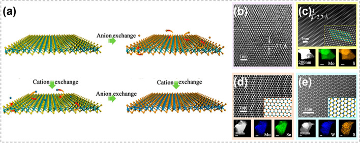
Atomic substitution applied in the synthesis of different dimensional transition metal chalcogenide (TMC) is dissertated.
The controllable synthesis and property modification realization with atomic substitution or ion exchange are introduced.
The substitution principle and mechanism in different TMCs are concluded.
Keywords: Transition metal chalcogenides, Atomic substitution, Ion exchange, Low-dimensional materials, Controllable synthesis
Abstract
In recent years, low-dimensional transition metal chalcogenide (TMC) materials have garnered growing research attention due to their superior electronic, optical, and catalytic properties compared to their bulk counterparts. The controllable synthesis and manipulation of these materials are crucial for tailoring their properties and unlocking their full potential in various applications. In this context, the atomic substitution method has emerged as a favorable approach. It involves the replacement of specific atoms within TMC structures with other elements and possesses the capability to regulate the compositions finely, crystal structures, and inherent properties of the resulting materials. In this review, we present a comprehensive overview on various strategies of atomic substitution employed in the synthesis of zero-dimensional, one-dimensional and two-dimensional TMC materials. The effects of substituting elements, substitution ratios, and substitution positions on the structures and morphologies of resulting material are discussed. The enhanced electrocatalytic performance and photovoltaic properties of the obtained materials are also provided, emphasizing the role of atomic substitution in achieving these advancements. Finally, challenges and future prospects in the field of atomic substitution for fabricating low-dimensional TMC materials are summarized.
Introduction
The diversity in types, structures, and properties of transition metal chalcogenides (TMCs) has led to their wide application prospects in devices, energy, and catalysis [1–3]. Especially those with reduced dimensions, including zero-dimensional (0D), one-dimensional (1D) and two-dimensional (2D) structures, have attracted significant attention due to their unique properties differing from their bulk counterparts [4–9]. To realize the applications of low-dimensional TMC materials in various scientific and technological fields, it is essential for these materials to exhibit well-defined optical, electronic, magnetic, and catalytic properties. Thereby, the synthesis methods that enable the precise control over the structures, morphologies and compositions of TMC materials are highly desired.
In the past few decades, different synthesis strategies for TMC materials have been developed, such as thermal injection and hydrothermal synthesis for 0D and 1D TMCs [10, 11], chemical vapor deposition (CVD) and molecular beam epitaxy (MBE) methods for 2D TMCs [12–15]. Although TMC materials with different sizes and morphologies have been realized, their qualities and compositions are generally limited [16, 17]. Due to the complex dynamics of reactions that involve multiple components, the controllability of direct synthesis methods is restricted. In contrast, atomic substitution shows great advantages in controlling the shapes, morphologies and compositions of multi-element materials. To date, the synthesis of various TMC structures have been realized by atomic substitution methods, including single binary compounds, doped materials, alloys, heterostructures and others [18–27].
As a post-processing technique, atomic substitution provides opportunities for precise engineering and customization of the desired properties of multi-element materials, and therefore serves to address the limitations of direct synthesis methods. By this method, great achievements have been made in TMCs synthesis and property modulation. For example, to achieve TMC materials with desired electronic or catalytic properties, ion exchange methods are commonly employed to tune the composition of the transition metal and chalcogens [28–33]. Moreover, the substitution reaction has the potential in inducing structural transformation, providing a promising pathway for synthesizing new materials or those are difficult to obtain directly [34–39]. For instance, through a moderate expansion of the anion sublattice during the substitution reaction process, it is possible to achieve metastable core@shell heterostructures without the formation of strain-induced defects at the interface, despite of a moderate lattice mismatch between core and shell [40]. These metastable heterostructures can hardly be directly synthesized by conventional growth methods, due to thermodynamically limited [41, 42]. Such controlled structural evolution not only expand the range of accessible materials but also enable the exploration for novel properties and functionalities, which is definitely advances the field of nanoscience.
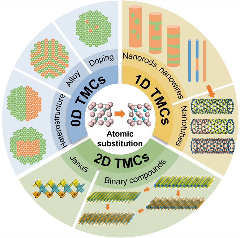
The fast development of atomic substitution methods has made the precise synthesis of TMC materials with well-controlled properties possible. Here, we reviewed recent progresses in the synthesis and modulation of low-dimensional TMC materials, including 0D, 1D and 2D, achieved by atomic substitution methods. In the 0D section, the principles of atomic exchange in solution are discussed. The synthesis of substituted TMCs through both the cation exchange reactions and anion exchange reactions is presented. Moving to the 1D section, the synthesis of TMC nanorods, nanowires, nanotubes and nanobelts is summarized, highlighting the strategies employed to achieve their controlled growth. In the 2D section, the initiation mechanisms for atomic substitution within TMC films are introduced, which typically originate from vacancies, grain boundaries or edges. The substitution processes for 2D TMCs are discussed, categorized as either complete substitution or partial substitution, depending on the extent of the process. Complete substitution shows great potential in fabricating ultra-thin TMC films that cannot be directly synthesized, whereas partial substitution is widely employed for the synthesis of heterostructure materials, Janus structures, alloys and so on. The improved electrocatalytic and photovoltaic properties of the obtained TMC materials are also presented. Finally, we conclude this review by discussing the limitations and future. This comprehensive review provides valuable insights into the design principles, structural characteristics, and potential applications of low-dimensional TMC materials, which will greatly benefit the development of next-generation TMC devices and technologies.
0D TMCs
0D TMC materials refer to structures with all dimensions being in the range of 1 ~ 100 nm, which typically consist of transition metals from Group IB to Group IIB and chalcogens, with a composition ratio of M:X ranging from 1:1 to 1:2 [43–45]. Their unique physical and chemical properties make them to be highly promising for photoluminescence [46, 47], photocatalysis [48, 49], photothermal therapy [50, 51], etc. To date, many strategies have been developed to synthesize 0D TMC materials, such as hot injection [52, 53], topological chemical synthesis [54, 55] and solvothermal (or hydrothermal) method [56, 57]. Among them, the topological chemical synthesis approach accompanied with atomic substitution shows great advantages in precisely tailoring the compositions, morphologies and structures of materials [58–60]. It is worth noting that for 0D TMC materials, atomic substitute reactions typically take place within solutions containing ionic compounds, known as ion exchange reactions.
Since Alivisatos and coworkers demonstrated the potential of ion exchange in fabricating inorganic nanocrystals with diverse compositions, sizes, shapes and structures [61], this synthesis approach has gained widespread exploration for generating various materials. To date, ion exchange has become as a versatile tool for synthesizing TMC materials. In this section, the principles of ion exchange reactions were discussed, followed by the employment of ion exchange reactions in synthesizing various 0D TMC materials, including single-, doped-, alloyed- and hetero-nanocrystals.
Principles of Ion Exchange Reactions
Generally, ion exchange reactions are reversible, with the reaction direction dominated by the thermodynamic factors of the reactants and products. Both the Gibbs free energy of reactions (ΔGr) and bond dissociation energies (BDEs) are essential for predicting the thermodynamics of ion exchange reaction [62, 63]. ΔGr determines whether the reaction is thermodynamically favorable or not, and the reaction can proceed spontaneously when ΔGr < 0. BDEs theory suggests that materials with stronger BDEs are more likely to participate in ion exchange reactions, especially when various ions are miscible. BDEs of some common metal chalcogenides are listed in Table 1. The synthesis of tellurides is more challenging compared to sulfides and selenides, owing to the lower BDEs between metal and Te atoms.
Table 1.
Comparison of bond dissociation energies (BDEs) of some metal chalcogenides
| Compound | BDEs (kJ mol−1) | Compound | BDEs (kJ mol−1) |
|---|---|---|---|
| Ag2S | 216.7 ± 14.6 | CdSe | 127.6 ± 25.1 |
| Ag2Se | 210.0 ± 14.6 | CdTe | 100.0 ± 15.1 |
| Ag2Te | 195.8 ± 14.6 | ZnO | 280.1 |
| Cu2O | 259.0 ± 30.0 | ZnS | 224.8 ± 12.6 |
| Cu2S | 274.5 ± 14.6 | ZnSe | 170.7 ± 25.9 |
| Cu2Se | 255.2 ± 14.6 | ZnTe | 117.6 ± 18.0 |
| Cu2Te | 230.5 ± 14.6 | PbS | 398.0 |
| CdO | 236.0 ± 84.0 | PbSe | 302.9 ± 4.2 |
| CdS | 280.5 ± 20.9 | PbTe | 249.8 ± 10.5 |
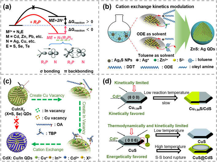
The thermodynamics and kinetics of ion exchange reactions can also be effectively mediated by factors like ligands, solvents and crystal structures, etc., which are not taken into account in the above two theories. Currently, Pearson’s hard and soft acid base theory is widely used for assessing the affinity between metal ions and ligands/solvents [64]. It offers a framework to predict the process of ion exchange reactions, with hard acids showing a preference for hard bases and soft acids favoring soft bases. Phosphines as soft Lewis bases are common ligands in ion exchange reactions. Depending on the nature of the R groups, phosphines can form either σ bonding or π back-bonding with metal. In 2015, Zhang’s group intuitively characterized the distinct coordination capabilities between various metal cations and phosphine ligands, providing direct evidence for cation exchange (CE) reactions induced by phosphine ligands [65]. As shown in Fig. 1a, for a thermodynamically unfavorable exchange process (ΔGr > 0), the introduction of phosphine ligands can not only facilitate the solvation and extraction of cations from the reactants but also enhance the desolvation and incorporation of cations into the products. This effectively changed the sign of ΔGr (ΔGr < 0), making the reaction thermodynamically favorable. Based on this finding, a series of metal@semiconductor core@shell nanocrystals were successfully obtained by choosing appropriate phosphine ligands. Solvents also play a crucial role in determining the kinetics of ion exchange reaction. As illustrated in Fig. 1b, Bai et al. synthesized high-quality Ag-doped ZnS quantum dots (QDs) and Au@ZnS core–shell nanocrystals using different solvents [66]. It was found that even utilizing the same thiol ligand, CE reactions in different solvents shows distinct reaction rates, suggesting diverse coordination abilities between metal cations and solvents.
Fig. 1.
Schematics of ion exchange reaction principles a Thermodynamic scheme of the cation exchange (CE) reactions initiated by the phosphine ligands. Reproduced with permission [65].
Copyright 2015, John Wiley and Sons. b Schematic of the thiol ligands and solvents combination coordinated CE reactions. Reproduced with permission [66]. Copyright 2019, John Wiley and Sons. c Schematic of CE reaction triggered by surface vacancy engineering. Reproduced with permission [67]. Copyright 2020, Elsevier. d Scheme of partial CE reactions in djurleite Cu1.94S nanodisks and covellite CuS nanodisks. Reproduced with permission [68]. Copyright 2022, RSC Pub
The influence of defects and crystal structures of reactants on the process of ion exchange reaction cannot be ignored. Vacancy defects act as vehicles to promote ion diffusion as they can move quickly within the crystal during reactions. As illustrated in Fig. 1c, using engineered CuInX2 nanocrystals with abundant surface vacancies as the reactant, Bai et al. successfully synthesized Cu/In dual-doped CdX (X = S, Se) nanocrystals [67]. The creation of Cu and In vacancies are found to be critical to overcoming kinetic energy barriers and effectively accelerating Cd2+ diffusion process. As for the crystal structure, it mainly affects the diffusion of ion into host materials. In Fig. 1d, due to the similar structures between djurleite Cu1.94S and wurtzite CdS, Cu+ in djurleite Cu1.94S nanodisks can be easily substituted by Cd2+ at a low temperature [68]. It is worth noting that the CE reactions from the top of Cu1.94S nanodisks were kinetically limited due to the absence of vacancies along the < 100 > direction, resulting in the formation of segmented Cu1.94S/CdS nanodisks. In contrast, Cu2+ in covellite CuS were hardly replaced by Cd2+ at a low temperature, due to the high energy barrier for breaking S–S covalent bonds. At a high temperature, S–S bonds underwent reduction, leading to the reorganization of sulfur anion frameworks. As a result, the substitution of Cu2+ in CuS by Cd2+ along the lateral directions became energetically favorable. However, CE reactions starting from the top of the CuS nanodisks were limited because of the large mismatch of S–S distances between CuS (001) and CdS (001), resulting in the formation of CuS@CdS nanodisks.
Complete Exchange
To date, the ion exchange strategy has been widely used for controllable synthesis of TMC materials with tailored morphologies, structures and hetero-interfaces. Especially, it allows synthesis of TMC materials with unique compositions and morphologies that cannot be obtained by direct seeded growth. For example, metal@semiconductor core@shell heterostructures through ions exchange of semiconductor shells with guest ions showed atomically organized interfaces and high-crystalline semiconductor shells, and such structures can be achieved even there is a large lattice mismatch between metal and semiconductor components [65, 69–71]. These structures generally enable efficient injection of hot electrons triggered by surface plasmon resonance, which provides an avenue to promoting the efficiency of photocatalysis, photoelectrochemical cells and photovoltaics.
Syntheses of 0D TMCs via CE Reactions
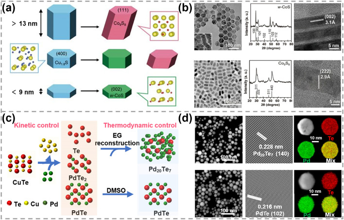
According to the type of exchanged element, ion exchange reactions can be categorized into the CE reactions and anion exchange (AE) reactions. CE reactions involve the release of cations from the reactant TMC material and the exchange of other cations from the solution into TMC material. After CE reactions, the anion framework can be either preserved or reconstructed [63, 72–74]. As shown in Fig. 2a, b, the original S framework can be maintained when the height of Cu1.8S nanocrystals was less than 9 nm, resulting in the formation of wurtzite cobalt sulfide (CoS) [38]. Once the height exceeds 13 nm, structure reconstruction driven by thermodynamics occurred and cubic cobalt pentlandite (Co9S8) nanocrystals was obtained.
Fig. 2.
Synthesis and characterizations of 0D TMC materials obtained by CE reactions. a Schematics of height-dependent phase transformation of Cu1.8S nanocrystals during the CE process and b corresponding transmission electron microscopy (TEM) images, X-ray diffraction (XRD) patterns, high-resolution transmission electron microscopy (HRTEM) images. Reproduced with permission [38].
Copyright 2021, The American Association for the Advancement of Science. c Schematic showing the kinetic control and thermodynamic control for the CE process of PdTe and Pd20Te7 nanospheres synthesis. EG represents ethylene glycol and DMSO represents dimethyl sulfoxide. d TEM, HRTEM images of PdTe2 and Pd20Te7 nanospheres and corresponding energy-dispersive X-ray spectroscopy (EDS) elemental mapping images. Reproduced with permission [60]. Copyright 2022, Springer Nature
CE reactions have been widely used for the controllable synthesis of M–S and M-Se materials [55, 75–80]. However, the transformation of M–Te materials is often accompanied with significant alteration in morphology, making the synthesis of M–Te materials with desired morphologies and structures to be more challenging [63, 81]. Recently, Feng et al. synthesized noble metal tellurides (NMTs) with tailored morphologies (0D, 1D, 2D and 3D), compositions (Pd/Pt/Rh/Ru/Ag/Au-based NMTs) and structures via CE strategy by regulating the interactions between solvents and noble metal cations [60]. As displayed in Fig. 2c, Cu2+ within the CuTe template can be rapidly exchanged by Pd2+ based on the kinetic control, leading to the formation of Te, PdTe2 and PdTe. The products can be further tuned by controlling the thermodynamic process. In dimethyl sulfoxide, Pd2+ formed strong bound with the sulfoxide group, leading to a low content of free Pd2+ in solution for CE reactions. This resulted in the formation of Pd-poor NMTs, specifically PdTe. In contrast, there were more Pd2+ cations available for CE reactions in ethylene glycol due to its much weaker interaction with Pd2+. As a result, a Pd-rich structure characterized as Pd20Te7 was formed. Despite of the reconstruction of anion framework, the original nanosphere shape was retained in Pd20Te7 and PdTe products, showing highly crystalline structures with a uniform element distribution (Fig. 2d). In this strategy, the kinetic control and solvent-dependent thermodynamic control were revealed to be critical for the successful synthesis. This CE reaction provide a feasible and flexible method for the achieving of desired NMTs.
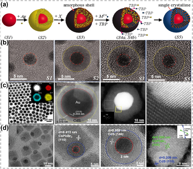
In addition to the synthesis of pure phase of TMCs, CE reactions also provide a promising strategy for fabricating metal–semiconductor heterostructures. In Table 2, representative examples of such heterostructures with varying lattice mismatches are listed. Notably, CE reactions demonstrate a great potential in synthesizing heterostructures with substantial lattice mismatches, which is typically beyond the capability of conventional epitaxial growth methods. In 2010, Zhang et al. reported a synthetic route for metal@semiconductor core@shell heterostructures [69], as exhibited in Fig. 3a, b. Starting from the metal core, an amorphous shell of Ag2X (X = S, Se, Te) was obtained first, serving as a crucial platform for the following reverse CE reactions. Tributylphosphine was then selected as the phase-transfer agent to exchange free cations (Mn+) in solution with Ag+ in the amorphous matrix, in order to obtain Au@MX (X = S, Se, Te) heterostructures. Various core@shell heterostructures were achieved finally, including Au-CdSe, Au-CdTe, FePt-CdS, Au-PbS, Au-ZnS and Pt-CdS. These heterostructures all possessed atomically organized interfaces and monocrystalline shells. The lattice structures of TMC shells were found to be independent of the core metal, suggesting their non-epitaxial relationship. With the development of this reverse CE reaction-facilitated non-epitaxial growth strategy, the size of synthesized high-quality metal@semiconductor heterostructures had reached to 50–100 nm [48], achieving breakthroughs from quantum scale to nanoscale (Fig. 3c). In these studies, the shell growth was guided by its thermodynamic property, and the obtained structure was independent of the core. The CE reaction is beneficial for circumventing the limitations imposed by epitaxial strategies and offers a precise and controllable way in the synthesis of core@shell heterostructures with atomically organized interfaces.
Table 2.
Representative examples of reported core@shell heterostructures with different lattice mismatches
| Core | Shell | Lattice mismatches (%) | Overall morphology | Refs. |
|---|---|---|---|---|
| PbTe | CdTe | < 1 | Sphere | [29] |
| PbSe | CdSe | ~ 1 | Sphere/rod/cube | [82, 83] |
| PbS | CdS | ~ 2 | Rod/sphere | [84, 85] |
| CuInS2 | ZnS | 2–3 | Sphere | [86] |
| CdSe | CdS | 3.8–3.9 | Rod/sphere/tetrapod | [87, 88] |
| CdTe | ZnTe | 6.5 | Sphere | [89] |
| CdTe | CdSe | 6.7–7.1 | Sphere/prolate-shape | [90, 91] |
| CdTe | ZnS | 19.8 | Sphere | [89] |
| Ag | CdS | 35.3 | Triangle | [92] |
| Au | CdS | 42.7 | Sphere | [69] |
| Pt | CdS | 48.3 | Sphere/cube | [65, 69] |
| Au | CdSe | 49.1 | Sphere/dumbbell | [69, 93] |
| Au | CdTe | 58.9 | Sphere/rod | [69, 94] |
Fig. 3.
Synthesis and characterizations of 0D metal–semiconductor heterostructures obtained by the reverse CE reaction-facilitated non-epitaxial growth strategy. a, b Schematic showing different growth stages of Au@CdS heterostructures and the corresponding HRTEM images. Reproduced with permission [69].
Copyright 2010, The American Association for the Advancement of Science. c TEM images of Au@ CdS heterostructures and high-angle annular dark-field scanning TEM (HAADF-STEM) images with corresponding elemental mapping images. Reproduced with permission [48]. Copyright 2018, Elsevier. d TEM and HAADF-STEM images of Au@CdS/CsPbBr3 heterostructures. Reproduced with permission [71]. Copyright 2022, John Wiley and Sons
This non-epitaxial growth strategy also shows a great potential in manipulating the compositions and structures of heterostructures [71, 95]. For instance, by maneuvring interfacial strain between metal and semiconductor components, non-concentric Au@CdX heterodimer structures were achieved [70]. The tunable relocations of plasmonic Au to CdX (X = S, Se, Te) in quantum size region allowed for a high degree of tunability in coupling their optoelectronic properties with other structures. By a combined non-epitaxial/epitaxial strategy, Au@CdS/CsPbBr3 ternary heterostructures with atomically organized interfaces were obtained (Fig. 3d). These resulting Au@CdS/CsPbBr3 heteronanocrystals generated remarkably long-lived plasmon-induced charge carriers with lifetime up to nanosecond timescale [71]. This development further expanded the applications of the reverse CE reaction-facilitated non-epitaxial growth strategy.
Syntheses of 0D TMCs via AE Reactions
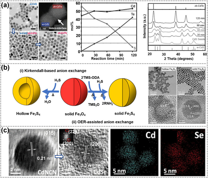
The process of AE reactions refers to exchanging anions in the reactant material with other anions. Compared with cations, the diffusion of anions is much slower within the 0D TMC nanocrystals due to their large ionic radii and large diffusion barrier. Consequently, AE reactions usually require higher reaction temperatures and longer reaction times, which contributes to a more manageable and controllable reaction process. As displayed in Fig. 4a, by performing the AE reactions of S2− by Te2− at 260 °C, the wurtzite CdS nanocrystals can be gradually transformed into zinc blende CdTe [96]. During the AE process, the size of the CdTe phase increased gradually, and spontaneous phase segregation occurred between CdS and CdTe due to their different phase structures. As the reaction continued, the complete transformation to a high-crystalline zinc blende CdTe was achieved at 120 min.
Fig. 4.
Synthesis and characterizations of 0D TMC materials obtained by the anion exchange (AE) reactions. a Synthesis illustrations of w-CdS/zb-CdTe heterodimers and corresponding TEM and HAADF-STEM images. Reproduced with permission [96].
Copyright 2011, American Chemical Society. b Illustrations showing the synthesis of hollow Fe3S4 and solid Fe3S4 nanocrystals and corresponding TEM and HRTEM images. OER represents an oxygen extracting reagent, TMS-ODA represents (Z)-N-trimethylsilyloctadec-9-en-1-amine and TMS2O represents bis-(trimethylsilyl) oxide. Reproduced with permission [97]. Copyright 2020, American Chemical Society. c Illustrations showing the synthesis of MX nanoparticles (M = Cd, Mn; X = S, Se) and corresponding HRTEM image as well as EDS elemental mapping images. Reproduced with permission [98]. Copyright 2019, American Chemical Society
Besides, AE reactions not only occur between chalcogens but can also take place between other elements. As shown in Fig. 4b, Lim et al. synthesized morphology-conserving Fe3S4 nanocrystals by AE reactions with the aid of oxygen extracting reagents [97]. In the AE process, the extraction of oxygen and subsequent formation of an amorphous phase acted as accelerants for the diffusion of incoming S2− ions, leading to the formation of morphology-conserving Fe3S4 nanocrystals (Fig. 4bii). Conversely, in the absence of oxygen-extraction agents, the formation of hollow Fe3S4 nanocrystals was inevitable, due to the imbalance in the diffusion between outgoing and incoming ions (Fig. 4bi). The oxygen extracting reagents assistant method has a great advantage in the synthesis of designed 0D nanocrystals without voids. This strategy illustrated new possibilities for the synthesis of various TMCs regardless of their shape and crystal structure. Jia et al. found that quasi-linear NCN2− in MNCN (M = Cd, Mn) nanoparticles can also be exchanged by X2− (X = S, Se) in colloidal solution (Fig. 4c). The quasi-linear NCN2− generated open space within the crystal lattice, effectively accommodating internal stress induced by AE reactions. As a result, the morphology and crystallinity were retained throughout the AE process. Besides, the anisotropic lattice of [NCN]2− anions was revealed to be critical in avoiding diffusion rate disparities and lattice collapse that occurred in single-atom anion compounds [98].
Partial Exchange
Compared with the complete exchange, partial anions/cations exchange process shows great advantages to synthesize doped, alloyed, and heterostructure TMC materials [10, 66, 99–104]. These materials have been widely reported due to their enhanced properties and optoelectronic applications [105–107]. For example, the deep-site doping enabled by reverse CE reactions can lead to nanocrystals with improved fluorescence quantum yields and lifetimes [100]. Core@shell QDs with continuously graded semiconductor shells prepared by ion exchange reactions show a strain-free interface and well-confined exciton, which are promising in optoelectronic applications of luminescent solar concentrators, light emitting devices and laser [108, 109]. Moreover, the ion exchange reaction provides possibilities for achieving metastable or non-equilibrium nanostructures, which cannot be obtained by conventional hot injection synthesis [42, 110]. In this section, we discuss the status of partial exchange in preparing doped, alloyed and hetero-structured TMC materials. In general, alloyed and doped materials were obtained in the case of reactants and products were miscible; otherwise, multi-domain heterostructures were formed.
Synthesis of 0D Doped TMC Materials
Due to the inherent self-purification effects, the host matrix often exhibits a tendency to expel dopant ions toward the surface of nanocrystals during doping process, especially at high temperatures [100]. Therefore, a delicate balance in precursor reactivity is required for precise control over the incorporation of dopants, which is quite challenging in a direct synthesis process. In contrast, the ion exchange strategy shows great advantages in the synthesis of doped materials, as it allows for the temporal separation of nanocrystal growth from the incorporation of impurities [63]. By controlling the kinetics of partial CE process, it is possible to retain a small quantity of “impurities” within the host matrix, serving as dopant ions. To date, various 0D doped TMC nanocrystals have been reported by direct CE reactions, such as Yb-doped PbIn2S4 nanocrystals [111], Ag-doped CdSe nanoparticles [112], Mn-doped ZnSe QDs [113] and Cu- or Ag-doped Cd1-xZnxSe nanocrystals [114]. All of these materials exhibited a much broader tunable spectrum range and enhanced optoelectronic properties, depending on the concentration of dopants.
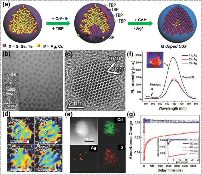
Besides, as shown in Fig. 5a, Zhang et al. synthesized M-doped CdX (M = Ag, Cu and X = S, Se, Te) QDs by reverse CE reactions. By controlling CE process of M+ and Cd2+, the deep-site heterovalent doping can be achieved. Transmission electron microscopy (TEM) and high-resolution transmission electron microscopy (HRTEM) images in Fig. 5b, c show that the obtained QDs were monodispersed and highly crystalline. Figure 5d, e confirms that Ag atoms were effectively retained within the center of CdS QDs, suggesting the realization of deep-site heterovalent doping rather than a surface doping [100]. Deep-site heterovalent doping effectively avoided the self-purification process. The efficient energy transfer from the intrinsic conduction band to the deep dopant energy level quenched exciton emission and inspired stable and strong dopant emission (Fig. 5f, g). This synthesis paves the way for the incorporation of dopant ions into specific sites of nanocrystals.
Fig. 5.
Synthesis and characterizations of 0D doped TMC materials by CE reactions. a Illustrations showing the synthesis process of M-doped CdX (M = Ag, Cu; X = S, Se, Te) nanocrystals. TBP represents tributylphosphine. b TEM image, c HRTEM images, d strain mapping images and e EDS elemental mapping images of Ag-doped CdS quantum dots (QDs). f Room temperature steady-state fluorescence spectra with different Ag-dopant concentrations, and the inset shows a digital photograph of fluorescence under 365 nm ultraviolet irradiation. PL represents photoluminescence. g Kinetic traces at representative wavelengths are also shown (pump laser wavelength: 390 nm). Reproduced with permission [100].
Copyright 2015, John Wiley and Sons
Synthesis of 0D TMC Alloys
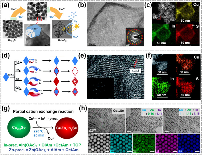
In direct synthesis of alloyed TMC materials, a significant challenge arises from the necessity of balancing the reactivities of precursors, which makes it difficult to attain the desired atomic composition. However, the development of CE reactions provides a feasible approach to overcome this challenge. Based on this strategy, binary, ternary and even quaternary alloyed nanocrystals have been realized [18, 106, 115–118]. As exhibited in Fig. 6a–c, Li et al. synthesized hollow CuInS2 nano-dodecahedrons with a uniform elemental distribution by using Cu2-xS as reactants. The formation of hollow structure was attributed to different rates of Cu+ extraction from Cu2-xS nanocrystals and In3+ incorporation into them [18]. The diffusion kinetics of Cu+ and In3+ can be precisely manipulated by passivating the surface of Cu7S4 nanocrystals. As shown in Fig. 6d–f, with an increased In3+/Cu+ ratio, the surface of Cu7S4 nanocrystals were passivated due to excess In3+ cations. As a result, a series of CuInS2 and Cu7S4@CuInS2 nanocrystals with intricate structures and uniform elemental distribution were obtained, which showed different photocatalytic abilities in singlet oxygen generation [116]. This research not only provides a flexible way to achieve nanocrystals with structural complexity and diversity, but also have an important significance in understanding the reaction kinetics in ion exchange process.
Fig. 6.
Synthesis and characterizations of TMC alloys by CE reactions. a TEM images showing the structural evolution from Cu2-xS dodecahedrons to CuInS2 ones. b, c STEM images and corresponding EDS elemental mapping images of CuInS2 dodecahedrons. Reproduced with permission [18].
Copyright 2019, American Chemical Society. d The different products derived from In3+—for—Cu+ CE in Cu7S4 nanocrystals at different In: Cu ratio. e, f HRTEM image and the corresponding EDS elemental mapping images for the product in d with the In: Cu ratio of 1: 1. Reproduced with permission [116]. Copyright 2019, Royal Society of Chemistry. g Illustrations showing the synthesis of CuZnxInySe nanocrystals. h HRTEM images and corresponding EDS elemental mapping images of CuZnxInySe nanocrystals. Reproduced with permission [118]. Copyright 2023, American Chemical Society
In 2023, Thiel et al. used Cu2-xSe nanocrystals as templates to synthesize CuZnxInySe quaternary alloyed nanocrystals (Fig. 6g). HRTEM images and corresponding energy-dispersive X-ray spectroscopy (EDS) elemental mapping images demonstrated the complete transformation of Cu2-xSe nanocrystals into CuZnxInySe nanocrystals, while maintaining high uniformity in the distribution of Cu, Zn, In and Se elements (Fig. 6h). The photoluminescence test results showed that the synthesized CuZnxInySe nanocrystals exhibited excellent near-infrared photoluminescence, without the need for additional shell growth. This is notable because the most of developed protocols require an additional shell to achieve similar performance. In particular, the full width at half-maximum of their near-infrared photoluminescence was reduced to 150–190 meV, accompanied by an enhancement of photoluminescence quantum yield to 20%. Moreover, precise control over the In/Zn ratio was achieved, and it was observed that increasing the Zn content resulted in an observable blue shift [118]. Up to now, various 0D alloyed TMC materials have been realized by CE reactions, including ZnxCd13-xSe13 magic-size clusters [117], AgInS2 nanoparticles [119] and Au@Ag2ZnSnS4 core–shell nanocrystals [120], etc. This synthesis strategy not only offers a protocol for the precise construction of 0D TMC nanocrystals with desired structures and composition, but also contributes to enhancing the structural complexity and diversity to TMC materials.
Synthesis of 0D TMC Heterostructures
TMC heterostructures have attracted lots of attention due to their capacity to integrate diverse functions stemming from coupling between multiple components. In recent years, partial CE reactions have emerged as a valuable alternative to epitaxial growth for the synthesis of TMC heterostructures at relatively low temperatures [121]. It also shows great advantages in controlling the interface between two components. To date, both segmented heterostructures and core@shell heterostructures have been realized by partial CE reactions. In segmented heterostructures, different materials are arranged in distinct segments or regions, including Janus-like, striped and sandwich-like structures.
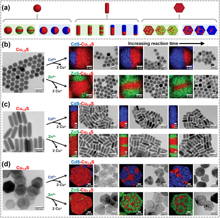
For the synthesis of segmented heterostructures, the ion mobility is usually high enough to facilitate the atomic arrangement of transformed domains into the lowest energy configuration. For instance, due to the high mobility of Cu ions, Cu2-xS reactants have been extensively employed for producing Cu2-xS/MS (M = Cd, Zn, Pb) segmented heterostructures. In Fig. 7a, Fenton et al. used different shaped Cu1.8S nanoparticles as templates in CE process. By adjusting reaction time, the extent of CE reactions involving Cu+ with Cd2+ or Zn2+ can be controlled [122]. As a result, various types of Cu1.8S/CdS or Cu1.8S/ZnS heterostructures were achieved successfully, including particles that contain asymmetric, patchy, porous, and sculpted nanoarchitectures. These heterostructures exhibited clear segmentation pattern and distinct internal interfaces (Fig. 7b–d), as confirmed by TEM images and corresponding EDS elemental mapping images [25]. This modular and divergent synthetic strategy enables the design and synthesis of complex nanoparticle systems. These researches have illustrated the reaction time is essential for the control of heterostructure with different morphology. These intricate colloidal nanoarchitectures have diverse potential applications, such as semiconductor–semiconductor interfaces for the controllable separation or confinement of excitons, precision integration of semiconductors and catalysts for light-driven chemical transformations, etc.
Fig. 7.
Synthesis and characterizations of the segmented heterostructures obtained by CE reactions. a Synthesis illustrations of Cu1.8S/CdS and Cu1.8S/ZnS segmented heterostructures. Reproduced with permission [122].
Copyright 2020, American Chemical Society. TEM images and corresponding EDS elemental mapping images of Cu1.8S b spheres, c rods and d hexagonal plates. Reproduced with permission [25]. Copyright 2018, The American Association for the Advancement of Science
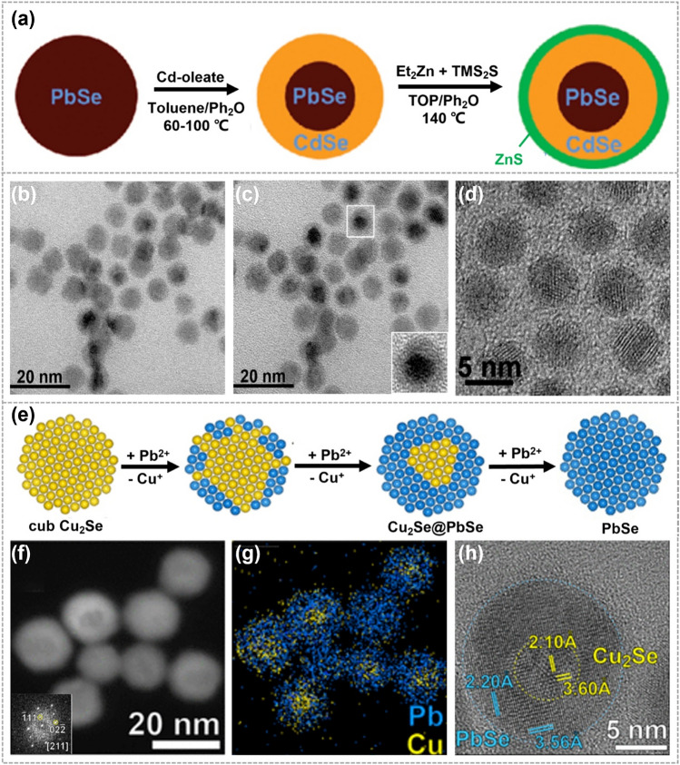
During the synthesis of core@shell heterostructures, CE reactions follow an isotropic-like exchange, without the generation of a significant strain between the two components. One of the extensively studied examples is PbX@CdX (X = S, Se, Te) core–shell heterostructures, where the core and shell have immiscible crystalline structures and a slight lattice mismatch. In 2008, Pietryga et al. applied CE reactions to prepare PbX@CdX QDs. As shown in Fig. 8a, PbSe QDs were exposed to a Cd-containing precursor, the partial substitution of Pb2+ by Cd2+ resulted in the formation of PbSe@CdSe QDs. The small lattice mismatch (∼1%) between the rock-salt PbSe and zinc-blende CdSe led to a relatively defect-free interface (Fig. 8b–d). The obtained PbSe@CdSe core@shell QDs exhibited significantly enhanced stability, thereby extending their operational temperature range [123]. In 2012, applying the similar strategy to PbSe nanocrystals of star, cube, and rod shapes, Casavola et al. achieved PbSe@CdSe core–shell heterostructures with corresponding shapes [83]. It was revealed that CE reactions proceeded dominantly in the (111) crystallographic direction, regardless of the shape of the initial PbSe QDs. This facilitated the formation of the Pb(111)—Se(111)—Cd(111) sandwich structure, resulting in a stress-free interface. Moreover, Pietryga et al. reported that a higher reaction temperature resulted in a thicker shell [124]. The thickness of CdSe shell up to 4 nm was achieved at a temperature of 200 °C, which displayed an additional infrared emission channel aside from the common visible range. The obtained heterostructures are a unique class of tuneable, dual-emitting, dispersible fluorophores, holding great potentials for labeling and photoluminescence microscopy. The critical factor of the core@shell heterostructure formation is to overcome the strain at interface resulting from lattice mismatch.
Fig. 8.
Synthesis and characterizations of the core–shell heterostructures obtained by CE reactions. a Synthesis illustrations of PbSe@CdSe QDs. Ph2O represents phenyl ether, TOP represents trioctylphosphine, Et2Zn represents diethyl zinc and TMS2S represents hexamethyldisilathiane. b Low-resolution image of 6.1 nm PbSe cores with 1.4 nm CdSe shells. c Low-resolution image of the same area as b, but tilted by 12° to enhance the diffraction contrast. d High-resolution image of PbSe@CdSe QDs, showing a relatively defect-free interface. Reproduced with permission [123].
Copyright 2008, American Chemical Society. e Cu2Se@PbSe heterostructures and f–h corresponding HRTEM images as well as corresponding EDS elemental mapping images. Reproduced with permission [40]. Copyright 2017, American Chemical Society
Precise control over the kinetics of CE reactions allows for the synthesis of core–shell heterostructures with a moderate lattice mismatch. However, these obtained core–shell heterostructures are usually metastable and prone to transform into more stable configurations, especially under conditions of elevated temperatures or intense light irradiation [80, 125–127]. For example, by performing partial Cu+ ions exchange with Pb2+ or Sn2+ within Cu2-xTe nanocubes, metastable Cu2-xTe@PbTe or Cu2-xTe@SnTe heterostructures were synthesized. The rapid and non-selective CE reactions took place on all facets of Cu2-xTe nanocubes, owing to abundant vacancies on the surface and high diffusion rate of Cu+ ions. Due to the significant deviation in lattice constants from that of Cu2-xTe, the formed PbTe or SnTe shells were polycrystalline. These metastable core@shell heterostructures transformed into stable Janus-like heterostructures when annealed at 200 °C in vacuum [42]. Additionally, it is possible to achieve core@shell heterostructures without the formation of strain-induced defects at the interface through a moderate expansion of the anion sublattice, even when there is a moderate lattice mismatch between core and shell. As shown in Fig. 8e, cubic Cu2Se nanocrystals were employed as host materials in CE reactions, and Cu2Se@PbSe heterostructures with a small expansion of the Se sublattice (∼6%) was formed by partially substituting surface Cu+ with Pb2+ [40]. The low diffusivity of Pb2+ ions into Cu2Se lattice and the absence of preferred entry positions in cubic Cu2Se led to the formation of a face-centered cubic Se anion sublattice, which was consistent with the host Cu2Se nanocrystals. During reaction, the moderate expansion of the Se sublattice was revealed to be critical in reducing strain and defects at the interface (Fig. 8f–h).
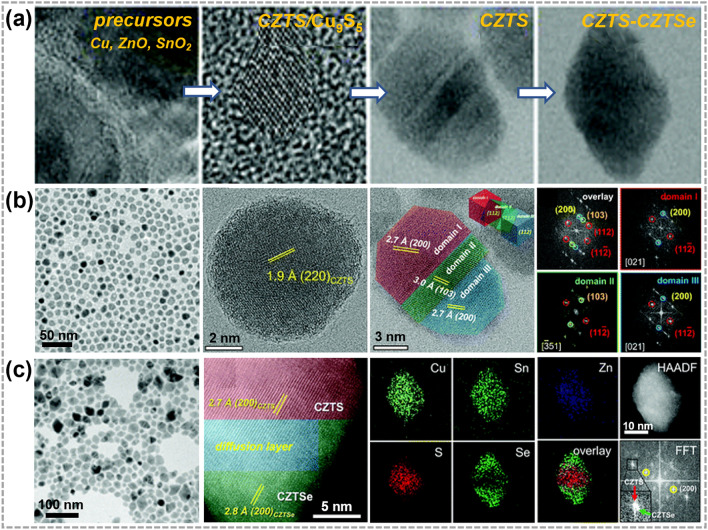
Moreover, CE and AE can be combined to synthesize high-quality heterostructures. Yin et al. reported the synthesis of quaternary kesterite Cu2ZnSnS4-Cu2ZnSnSe4 (CZTS-CZTSe) heterostructures by a combining CE and AE strategy, in which Cu, ZnO and SnO2 were chosen as precursors (Fig. 9a). The small lattice mismatch between Cu9S5 and CZTS nanocrystals allowed a transformation from Cu9S5 to CZTS with minimal changes in the S2− framework. This not only facilitated the incorporation of Zn and Sn but also helped to preserve the morphology of Cu9S5 nanocrystal (Fig. 9b). The pristine CZTS nanocrystals then served as a template for subsequent AE. HRTEM images in Fig. 9c show that Se treatment triggered the substitution of S2− within kesterite CZTS surface by Se2− during the AE process, and sandwich CZTS-CZTSe nano-heterostructures were obtained [128]. Compared with direct synthesis of pure kesterite CZTSSe nanoparticles, sandwich CZTS-CZTSe nano-heterostructures containing quaternary and quinary phases are more promising in promoting electron–hole separation in solar cell devices. Meanwhile, AE reactions overcame the energy barrier and energy difference between polycrystalline states that cannot be ignored in direct synthesis of CZTSSe nanocrystals.
Fig. 9.
Synthesis and characterizations of 0D TMC heterostructures obtained by a combining CE and AE strategy. a TEM and HRTEM images of synthesis Cu2ZnSnS4-Cu2ZnSnSe4 (CZTS-CZTSe) nano-heterostructure process. b TEM images of CZTS nanocrystals and fast Fourier transform (FFT) patterns of overlay, domain I (red), domain II (green), and domain III (blue). c TEM and high-resolution scanning TEM (HR-STEM) images of CZTS-CZTSe heterostructures and corresponding STEM-EDS elemental mapping images as well as corresponding FFT pattern of CZTS-CZTSe nanocrystals. Reproduced with permission [128].
Copyright 2021, RSC Pub. (Color figure online)
In summary, the ion exchange in 0D TMCs is a reversible reaction, in which both the kinetic control and thermodynamic control play essential roles in regulating the overall process. By the complete cation substitution, the synthesized core@shell heterostructure with substantial lattice mismatches exhibits atomically organized interface. The independence of shell from the core is beneficial for overcoming the strain at the interface imposed by epitaxial strategy. During the anion exchange, the adding of extra reagents provides new possibilities for the synthesis of desired nanocrystals. In partial ion exchange, the realization of controllability is a crucial point in achieving TMCs with exceptional properties. Numerous studies have demonstrated that by preciously controlling the reaction time and reactant concentration, it is possible to obtain heterostructures and alloys with desired compositions and morphologies. These studies also pave the way for controllable doping.
1D TMCs
Due to their adjustable quantum confinement effects, 1D TMC nanostructures hold great potential in applications of photonics and thermoelectricity [28, 129]. Compared with the conventional vapor–liquid-solid methods, atomic substitution offers an alternative route to create 1D TMC materials with intricate structures and notable compositional diversity [39, 101]. Similar to the case of 0D materials, low-cost colloidal methods are commonly employed for synthesizing 1D TMC materials. In this section, the development of ion exchange reaction in preparing nanorods, nanowires and nanotubes, is summarized.
Synthesis of 1D Nanorods
1D nanorods refer to nanostructures with one dimension much larger than the other two, exhibiting a distinct rod-like shape. This specific geometry enables the fine-tuning of their properties by varying the aspect ratios. To explore their fundamental properties and potential applications, great efforts have been dedicated to manipulate the morphologies and compositions of nanorods [28, 129–132].
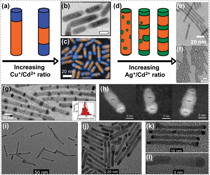
The substitution between atoms in nanorods is demonstrated to be selective, which plays an important role in determining the structure of products. For example, Sadtler et al. studied the partial transformation of CdS nanorods through CE reactions, as shown in Fig. 10a–g [131, 133]. In the case of Cu+–Cd2+exchange, the reaction started preferentially from either one or both ends of CdS nanorod, depending on Cu+/Cd2+ratio. This led to the growth of one or two Cu2S domains inward from the tip region. As a result, segmented Cu2S/CdS heterostructures were formed, in which the two subunits shared a flat interface perpendicular to the axial direction (Fig. 10a–c). The reason behind the selective nucleation and growth of Cu2S within CdS nanorods is the exceptional stability of formed CdS-Cu2S interfaces. In the case of Ag+-Cd2+exchange, the reaction occurred non-selectively and the formed Ag2S regions are randomly distributed within CdS nanorod. During the CE process, multiple Ag2S segments spanned the diameter of nanorod with a uniform size (Fig. 10d–g). The non-selective nucleation of Ag2S in CdS nanorod was ascribed to the negative chemical formation energies of CdS-Ag2S interface. However, as Ag2S regions extended within the nanorods, the influence of elastic energy became dominant, driving the ripening process of Ag2S regions and resulting in the reduction of interfacial area. The randomly distributed Ag2S regions finally evolved into a periodic pattern. The distinctions between CdS–Cu2S and CdS–Ag2S systems arise from differences in both the chemical favorability of bond formation and the elastic distortions at the interfaces. This offers an opportunity to manipulate the spatial configuration of components within heterostructures, and further control their chemical and physical properties.
Fig. 10.
Synthesis of hetero-nanorods by ion exchange process. a The morphology of CdS-Cu2S nanorods by CE reactions. b, c TEM image and color-composite energy-filtered transmission electron microscopy (EFTEM) image of the obtained CdS-Cu2S nanorods. d Illustration of CdS-Ag2S nanorods produced by CE methods. Reproduced with permission [133].
Copyright 2009, American Chemical of Society. e, f TEM images of the pristine CdS nanorods and obtained CdS-Ag2S nanorods. g TEM images of CdS-Ag2S nanorods with inset showing histogram of Ag2S segment spacing (center-to-center). Reproduced with permission [131]. Copyright 2007, The American Association for the Advancement of Science. h HAADF-STEM image of CdS/Pd4S hybrid nanorods. Reproduced with permission [134]. Copyright 2015, American Chemical Society. i Tip growth of Pd4S on CdS nanorods with a diameter of 5.9 nm. j The extensive growth of Pd4S on CdS nanorods with a broad size distribution. k Close-up of the sample shown in i. l HRTEM of a single CdS-Pd4S nanorod from the sample shown in j. Reproduced with permission [11]. Copyright 2011, John Wiley and Sons
The CdX/PbX system (X = S, Se, Te) has also been widely studied due to their excellent photoelectric property and chemical stability. Because PbX and CdX are immiscible, the exchange between Cd2+ and Pb2+ generally results in separated CdX/PbX heterostructures. Lee et al. demonstrated that the exposure of CdSe to Pb2+ ions lead to the transformation of wurtzite CdSe into rock-salt PbSe [134]. As shown in Fig. 10h, the replacement of Cd2+ ion was found to occur anisotropically, starting from the tips of nanorods and leading to the formation of interfaces parallel to the (0001) plane of nanorods. This is similar to the CdS/Cu2S case depicted in Fig. 10b [133]. Moreover, the Cd-to-Pb exchange was facet-selective and two tips of nanorods showed significant differences during transformation, because the (000 ) facet of CdSe nanorods is more active than the (0001) one. Explorations in this area enable precise control at the atomic level for CE, which could expand the possibility for designing CdX/PbX heterostructures. Under the similar reaction conditions, Zhang et al. prepared CdS/PbS and CdSe/PbSe Janus-like heterostructures by partial CE reactions [135]. The obtained structure exhibited excellent optoelectronic properties that can be customized for potential applications of various fields. By exposing CdS nanorods to Pd2+ containing solution, Shemesh et al. realized the synthesis of CdS/Pd4S segmented nanorods [11]. Similarly, the formation of Pd4S started from either one or both tips of CdS nanorods, resulting in the synthesis of segmented CdS/Pd4S structures with planar interfaces (Fig. 10i–l). These planar interfaces are critical in reducing interface energy and strain, thereby ensuring the stability of the structure.
Synthesis of 1D Nanowires
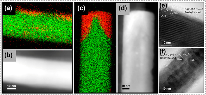
By CE reactions, Zhang et al. synthesized CdS@Cu2S core@shell nanowires with diameters of 30–40 nm and lengths of ~ 10 μm, as exhibited in Fig. 11 [129]. It was found that Cu+–Cd2+ exchange reaction occurred simultaneously at both side facets (Fig. 11a, b) and tips (Fig. 11c, d) of CdS nanowires, with a notable preference at the tips. The calculated transformation energy for nucleation from side facets was approximately seven times higher than that at tips [133]. Furthermore, solid-state diffusion enabled the penetration Cu ions into the inner regions of the CdS nanowires. This diffusion process resulted in the formation of core@shell nanowires, and the thickness of the shell increased as the reaction continued. Besides, the composition of resulting core@shell nanowire was found to be dependent on the Cu+/Cd2+ ratio. As shown in Fig. 11e, f, CdS@Cu2-xS nanowires were achieved under a Cu+/Cd2+ ratio of 0.5:1, while CdS@Cu2S nanowires with a thicker shell were formed under a Cu+/Cd2+ ratio of 1:1. Similar with the ion exchange reaction in 0D TMC alloys (Fig. 6d–f), by regulating the reactant concentration, this research provides a method for precisely control over the structure, composition, and crystal phases of nanowires, holding a promising prospect in various applications.
Fig. 11.
Synthesis and characterization of CdS@Cu2-xS nanowires by ion exchange process. a-d EDS element mapping images for Cd (in green) and Cu (in red) and corresponding STEM images. a, b Images showing the substitution started at the side surface of nanowires. c, d Images showing the substitution started at the tips of nanowires. e, f HRTEM images of CdS@Cu2–xS core@shell nanowires. e A core@shell nanowire obtained with a 0.5:1 Cu+/Cd2+ ratio, f a core@shell nanowire with increasing shell thickness obtained with a 1:1 Cu+/Cd2+ ratio. Reproduced with permission [129].
Copyright 2014, American Chemical Society. (Color figure online)
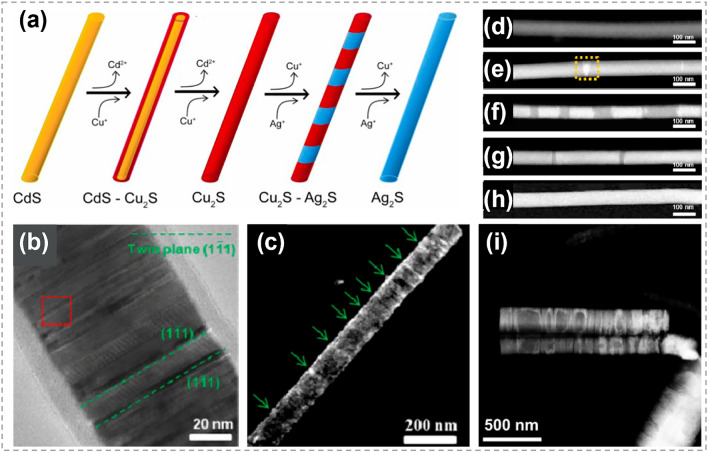
Tan et al. realized the controllable synthesis of multiple p-n segmented heterojunctions by a two-step CE strategy, as illustrated in Fig. 12a. Using single-crystal CdS nanowires as reactants, Cu2S nanowires with face-centered cubic (fcc) crystal structure were obtained after the complete exchange of Cd+ by Cu+. Figure 12b, c shows that there are abundant twin planes perpendicular to axial direction [28]. These twin boundaries offered active sites for the following exchanging between Cu+ and Ag+. The newly formed Ag2S segments were found to be parallel to the twin planes and elongate along the axial direction with the reaction proceeded, as shown in Fig. 12d–h. This suggests that the morphology of regular Ag2S–Cu2S heterojunctions can be well controlled by terminating CE process at a precise reaction time. This work highlights the significance of crystal structure and orientation of twin plane in determining the regularity and pattern of the resulting Cu2S–Ag2S heterostructures. As a comparison, irregular patterning was observed after Cu+–Ag+ exchange reaction in monoclinic Cu2S nanowires with twin planes not perpendicular to axial direction (Fig. 12i). These explorations provide two effective methods to control the morphology of nanowires by regulating the reactant concentration and reaction time, respectively. In addition, the ion exchange rate demonstrates noticeable location selectivity in both of the above studies.
Fig. 12.
Synthesis and characterizations of Cu2S-Ag2S heterostructure nanowires. a Illustration shows the formation process of Cu2S-Ag2S superlattice nanowires. b TEM image of a Cu2S nanowire transformed from a CdS nanowire. The twin planes are the (11̅1) planes. c Dark-field TEM image of a single Cu2S nanowire viewed along the [109] zone axis and presented by selecting the (11̅1) diffracted beam. The green arrows indicate locations of the (11̅1) twins. d-h HAADF-STEM images of the Cu2S-Ag2S nanowires formed. Reaction times are d 0 s, e 6 s, f 24 s, g 48 s, h 60 s. i HAADF-STEM image of Ag2S/Cu2S nanowires after CE reactions in monoclinic Cu2S structure. Reproduced with permission [28].
Copyright 2014, American Chemical Society. (Color figure online)
Synthesis of 1D Nanotubes
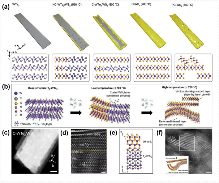
By taking advantage of large volume change during a certain CE reaction, Moon et al. realized the transformation of nanowires to nanotubes, as shown in Fig. 14 [39]. Ultra-thin Ag2Te nanowires were chosen as reactants, and were converted into CdTe nanowires in a Cd+ containing solution. During this process, the single crystalline structure of nanowires was preserved and the volume change was slight (Fig. 13a). Afterward, these CdTe nanowires were exposed to Pt4+ ions, and PtTe2 nanotubes with a wall thickness of 1–2 nm were formed. During this process, the mechanical stress caused by CE accumulated continuously, inducing the creation of voids in products. As a result, the single crystalline nanowires were transformed into polycrystalline PtTe2 nanotubes (Fig. 13b, c). This research illustrates the important effect of stress in the morphology transformation and is valuable for understanding the shape transformations in nanostructured materials under large stress.
Fig. 14.
Structure diagram and characterizations of TMC nanobelts by atomic substitution process. a The temperature-dependent synthesis of nanobelts via the substitution of chalcogen. NC-WTe2/WS2 represents non-curled WTe2/WS2, C-WTe2/WS2 represents curled WTe2/WS2 and C-WS2 represents curled WS2. b Schematic showing controlled conversion process at different temperatures. c HAADF-STEM image (scale bar: 30 nm) of the curled WTe2/WS2 grown at 600 °C. d, e Atomic-Resolution STEM image (scale bar: 1 nm) and atomic configurations showing the interface structure of the curled WTe2/WS2 heterostructure. f Plan-view Atomic-Resolution STEM image (scale bar: 2 nm) and atomic model showing the WS2 layer was deformed. Reproduced with permission [136].
Copyright 2020, John Wiley and Sons
Fig. 13.
Synthesis of PtTe2 nanotubes via the shape evolution in Cd+-Pt4+ exchanging process. a TEM image of CdTe nanowires, b TEM image of PtTe2 nanotubes derived from CdTe nanowires through CE reactions. c HRTEM image of a PtTe2 nanotube indexed as the hexagonal phase with lattice spacing of 0.28 nm along the [100] direction. The inset shows the Fourier transformed ring pattern of PtTe2 nanotubes. Reproduced with permission [39].
Copyright 2010, American Chemical Society
Synthesis of 1D Nanobelts
In 2020, Sim et al. introduced a novel approach for designing TMC heterojunctions by Metal Organic CVD [136]. Single-crystalline WTe2 nanobelts were adopted as the base structures and then sulfurized, as schematically shown in Fig. 14a. Depending on sulfurization temperature, Te atoms were replaced by S to different extents and various structures were formed, including non-curled WTe2/WS2, curled WTe2/WS2, curled WS2, and porous/curled WS2 as illustrated in Fig. 14b. At low temperatures, the substitution of Te by S predominantly started from edges, and the single-crystalline structure was maintained. At high temperatures, the conversion resulted in structurally deformed WS2 throughout the entire layers of nanobelt. Figure 14c shows the obtained curled WTe2/WS2 at 600 °C. The presence of an atomically ordered interface in Fig. 14d, e indicates that the lattices of two subunits were maintained in a coherent manner across the transition region, suggesting the heteroepitaxial stacking of WTe2/WS2 hybrids despite of their large lattice mismatch (≈8.8%). Figure 14f presents the as-prepared curled WS2 under 700 °C, despite many pores and deformed layers were observed throughout the entire area, the shape of nanobelt remained intact. Remarkably, the obtained 1D heterojunctions showed enhanced performance in the hydrogen evolution reaction as well as the long-term durability for electrocatalytic reactions, owing to the increased effective surface area and reduced electron-transfer resistance. Though the specific mechanism is not clear, the temperature effect in this research provides great reference for the exploration of the transformation between 1D TMCs.
Similar to the cases of 0D TMCs, the ion exchange method in 1D TMCs have illustrated the effects of temperature, reactant concentration and reaction time on both the composition and morphology, providing valuable references for controllable synthesis. Additionally, strain, surface energy and interfacial energy also show noticeable influences on the structural evolution during the substitution process. Moreover, both the exchange rate and initiation sites exhibit significant location dependence during the reaction.
2D TMCs
2D TMCs predominantly have a chemical formula of MX2, where M represents transition metals from Group IVB to Group VIIIB. In a 2D TMC structure, atoms within the same layer are chemically bonded, while those between layers interact through weak van der Waals force [9, 137, 138]. Depending on their compositions and phase structures, 2D TMCs display various electronic properties [139–145], showing great potential in applications of electronic devices, quantum devices, energy catalysis [146–149], etc.
In recent years, atomic substitution has been widely used in regulating the compositions and structures of 2D TMCs, and various materials have been obtained, including binary compounds, doped materials, alloys and heterojunctions [20–23, 150, 151], etc. Unlike the solution methods that are widely employed in 0D and 1D TMCs, CVD techniques are very popular for implementing atomic substitution process in 2D TMCs.
Initiation of Atomic Substitution
Owing to the ultra-thin structure, 2D TMCs provide a unique platform for studying the real-time process of atomic substitution. It is revealed that crystal defects, such as vacancies, grain boundaries (GBs), surfaces and edges, serve as starting points for the substitution process.
Vacancy-Initiated Substitution
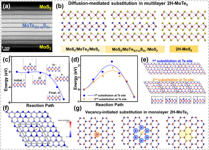
By sulfurizing sub-centimeter scale single crystalline 2H-MoTe2 thin film, Liu et al. achieved a corresponding single crystalline MoS2/MoTe2(1-x)S2x/MoS2 sandwich structure and proposed a Te vacancy-initiated and S diffusion-mediated transformation mechanism (Fig. 15a, b) [152]. The S substitution process started at Te vacancies in the top and bottom layers, and then progressed into the middle layers. Though the rate of substitution in the middle layers is limited by cross-layer diffusion of S atoms, the complete transformation is possible with the continuation of the process. Density functional theory (DFT) calculations also confirmed the role of Te vacancy, and found that there is no energy barrier for the occupation of S at Te vacancy site (Fig. 15c). In comparison, the energy barriers for the 1st and 2nd substitutions of Te in perfect MoTe2 structure are ~ 2.3 and 1.8 eV, respectively (Fig. 15d, e). It was noted that the substitution process is thermodynamically favorable. The lower energy barrier of the 2nd substitution was attributed to the strain field induced by the 1st substitution, as evidenced by the force mapping analysis (Fig. 15f). The compression caused by the initial substitution of S was beneficial for reducing the energy barrier of subsequent substitutions (Fig. 15g). This work provides an efficient way to acquire large-scale high-quality TMC films and heterostructures. Similarly, Taghinejad et al. realized the fabrication of MoS2xSe2(1-x) alloy via sulfurizing MoSe2 films. It was revealed that the driving force of substitution is much lower in CVD-grown MoSe2 films with abundant vacancies than that in exfoliated films with fewer vacancies [153].
Fig. 15.
Mechanism of atomic substitution initiated by vacancies. a Magnification HAADF-STEM cross-sectional image of the sulfurized MoTe2. b Diffusion-mediated substitution mechanism in multilayer MoTe2 (Red: Mo, yellow: S, and blue: Te) c Energy barrier for S substitution at Te vacancy. Insets are the path details. d Energy barriers and e path details for S substitution at Te sites (blue) in the perfect MoTe2 (orange) and after the insertion of first S. f Force map after the replacement of first S. g Diffusion-mediated substitution mechanism in multilayer MoTe2. Reproduced with permission [152].
Copyright 2021, American Chemical Society. (Color figure online)
The present of vacancies also plays an important role in promoting the substitution between metal atoms. By combining DFT calculations and experiments, Liu et al. [154] explored the Co substitution in MoS2 and revealed that the substitution is induced by sulfur vacancies. Chang et al. [155] found that the metal exchange between Sn and W can be promoted by producing S vacancies at high temperatures. To date, many strategies have been developed for vacancies creation to promote substitution processes, such as high temperature, ion beam bombardment and gaseous plasmas [21, 155, 156].
Grain Boundary-Initiated Substitution
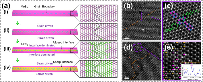
GBs have also been demonstrated to be initiation sites for atomic substitution. As shown in Fig. 16a, starting from intrinsic GBs of MoSe2, Zhu et al. obtained ultra-long MoS2 nano-channels successfully [157]. Figure 16b, c displays the pristine MoSe2 monolayer, where lots of active sites in 8|4|4|8 GBs can be observed. The formation process of MoS2 can be divided into three steps: (i) the chemisorption of S atoms near the GBs, (ii) the exchange between S and Se atoms, (iii) the desorption of Se atom. The second step has the highest energy barrier and is considered as the rate-limiting step. The energy barrier for replacing Se atoms at GBs is much lower, owing to the high in-plane tensile strain. The substituted S atoms then act as the nucleation center, leading to the continued growth of MoS2. Near the GB, MoSe2 was completely transformed into MoS2, while mixed structures that one Mo atom coordinates with S2, Se2, or S + Se atoms were formed at the interface of MoS2 and MoSe2, as shown in Fig. 16d, e. This study offers an excellent method for achieving narrow lateral heterostructures and precise control over the spatial scale of heterostructures.
Fig. 16.
Mechanism exploration in atomic substitution initiated by grain boundary. a Schematic showing growth of MoS2 channels. b, c Annular dark-field scanning transmission electron microscopy (ADF-STEM) images of intrinsic 60° GB (orange dashed line) within pristine monolayer MoSe2 and atomic arrangement of this GB (blue and purple circles: Mo and Se atoms) resembles that in MoS2 nano-channels. d, e ADF-STEM images showing part of MoSe2-MoS2 hybrid winding channel. The red arrows represent the sulfidation direction. Purple arrows mark 2Se atoms and yellow-purple arrows mark S + Se atoms, with line intensity profile showing in the inset. Reproduced with permission [157].
Copyright 2020, Spring Nature. (Color figure online)
Edge-Initiated Substitution
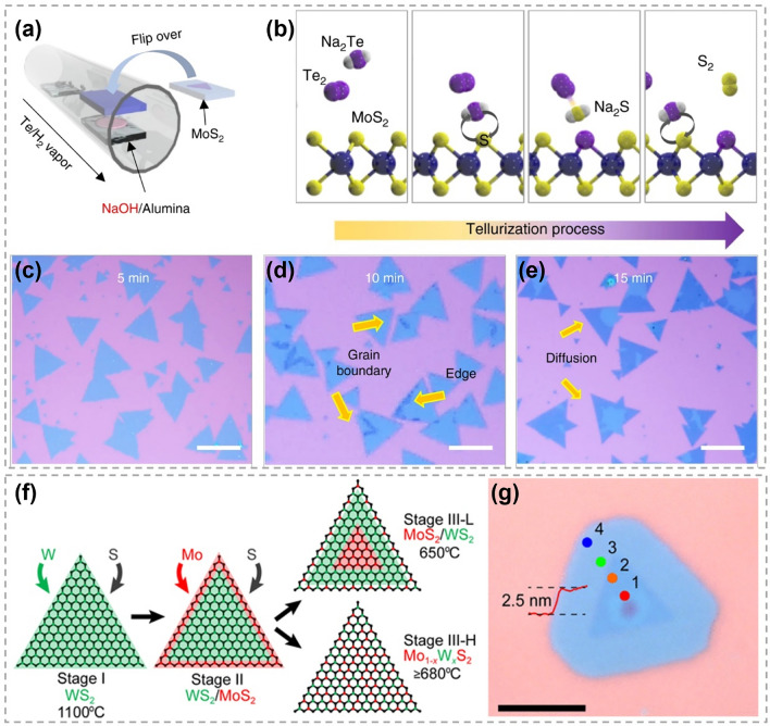
The enhanced reactivity of TMCs edges, attributed to their unsaturated chemical bonds, makes them more favorable for atomic substitution compared to the less reactive basal plane [136]. As displayed in Fig. 17a–e, Yun et al. converted monolayer MoS2 to MoTe2 in a Te-rich environment with the assistant of NaOH [158]. During the substitution process, Na2Te, which is the most probable Na-Te compound, acted as the driving agent to accelerate the tellurization of MoS2 and the dissipation of gaseous S2 (Fig. 17b). The optical images in Fig. 17c–e show the tellurization progress of MoS2. It is clear that MoTe2 primarily emerged along the edges and GBs, gradually extending toward the central area of MoS2. In contrast, the occurrence of substitution was not limited at edges at high temperatures, leading to random tellurization over MoS2 basal plane. Similarly, Bogaert et al. investigated the effect of temperature on the substitution between W and Mo in as-grown WS2 islands by CVD methods (Fig. 17f) [159]. At a relatively low temperature (650 °C), Mo substitution predominantly took place at WS2 edges. As a result, an in-plane MoS2/WS2 heterostructure with a sharp interface was formed (Fig. 17g). At a relatively high temperature (710 or 680 °C), the entropy contribution to the Gibbs free energy increased and led to the formation of Mo1-xWxS2 alloy. Therefore, it is possible to customize the pathway to form either TMC alloys or lateral heterostructures by controlling the substitution kinetics.
Fig. 17.
Mechanism of atomic substitution initiated by edge. a Alkali-metal-assisted transformation from MoS2 to MoTe2. b Schematic showing Na-assisted tellurization process. c-e Optical images showing the evolution from MoS2 to MoTe2. Reproduced with permission [158]. Copyright 2017, Springer Nature. f Illustration showing the substitution of W in WS2 by Mo at different temperatures (W atoms are shown in green, Mo atoms are red, S atoms are black). g Optical image of a typical heterostructure revealing a distinct core-ring structure. Scale bar is 5 μm. Reproduced with permission [159].
Copyright 2016, American Chemical Society. (Color figure online)
Synthesis of 2D TMC Binary Compounds
Substitution Between TMCs
The complete substitution of either transition metal atoms or chalcogen atoms within a TMC shows a great potential in converting the TMC to another type, as illustrated in Fig. 18a. By using exfoliated 2D TMC nanosheets as reactants, Duan et al. explored the feasibility and universality of ion exchange reactions in solution phase [27]. Three reactions were conducted successfully, including converting SnS2 into MoS2, converting MoS2 into MoSe2, and converting MoS2 into WS2. It was revealed that the ion exchange reactions were completely finished without specific adjustment of ion solubility, because the crystal structures and thermodynamic stabilities of the reactants and products were similar. HRTEM images in Fig. 18b–e show that the TMCs obtained by both CE and AE were highly crystalline with a relatively uniform elemental distribution. Compared with traditional CVD method, this work shows atomic substitution strategy as an alternative and flexible way to achieve new TMC materials.
Fig. 18.
Transformation between different TMCs by atomic substitution. a Schematic showing ion exchange in TMCs. b HRTEM image of a SnS2 nanosheet before CE reactions. c HRTEM and element mapping images of a MoS2 after CE. d STEM and element mapping images of a MoSe2 after AE. e STEM and element mapping images of a WS2 after CE. Reproduced with permission [27].
Copyright 2017, American Chemical Society
Oxygen-Chalcogen Substitution
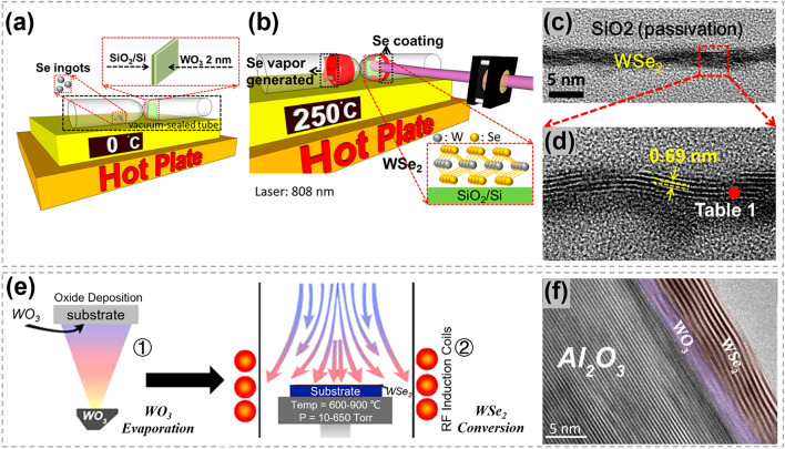
It is very common to prepare TMCs through utilizing chalcogens to reduce transition metal oxides in traditional CVD methods. In the process, transition metal oxides powder usually go through a high-temperature melting phase to yield metal precursors, followed by the nucleation and growth of TMCs. In contrast, the oxygen-chalcogen substitution strategy, based on transition metal oxide films, allows for the avoidance of the melting process. Chen et al. reported the selenization of WO3 thin films to produce WSe2 with the assistance of laser [160]. As shown in Fig. 19a, b, a WO3 film was directly deposited on a SiO2/Si substrate and placed in a vacuum-sealed quartz tube with Se ingots. The quartz tube was then placed on a hot plate to generate homogeneous Se vapor and a continuous wave laser was utilized to trigger the substrate heating. In the presence of selenium gaseous vapor, the amorphous WO3 film underwent a reduction process when the laser was irradiating on it. Layered WSe2 film was successfully achieved, as shown in Fig. 19c, d. Besides, through a process involving the patterning of the WO3 film and subsequent laser irradiation, patternable WSe2 fabrication was realized. Compared with thermal CVD method, the laser assistant substitution can achieve an ultrafast heating on the target part, making the synthesis process to be more controllable. This laser assisted reduction process was also demonstrated to have a great potential in the synthesis of other TMCs, such as MoS2, WS2, WSe2 [161–163]. Large area WSe2 have been synthesized by direct selenization of as-deposited WO3 films [164]. As shown in Fig. 19e, the WO3 films were deposited onto substrates via thermal evaporation first and then converted to WSe2 by exposing to dimethyl selenium in a cold wall reactor. As shown in the cross-section TEM image (Fig. 19f), 8–10 layers of WSe2 were generated on the WO3 film. Besides, the thickness of WSe2 can be effectively controlled by the thickness of WO3 film and the depth of selenization. This research proposed an effective route to synthesize TMC films with controllable and highly uniform thickness based on the transition metal oxide.
Fig. 19.
Synthesis of WSe2 by the oxygen-chalcogen exchange process. a Illustration showing 2 nm-thick WO3 on SiO2/Si and Se ingots was vacuum-sealed together. b Illustration showing the formation of WSe2 when heating up to 250 °C. c Across-sectional TEM image of WSe2. d HMTEM image revealing the interlayer distance of the WSe2. Reproduced with permission [160].
Copyright 2015, American Chemical Society. e Synthesis process of WSe2 converted from amorphous WO3 and hexagonal stabilized WO3 films. Thermal evaporated WO3 films were annealed via rapid thermal annealing and then converted to WSe2 via cold wall furnace. f TEM image of the obtained layered WSe2 structure and the unconverted WO3 film between sapphire and WSe2. Reproduced with permission [164]. Copyright 2015, IOP Publishing
Iodine-Chalcogen Substitution
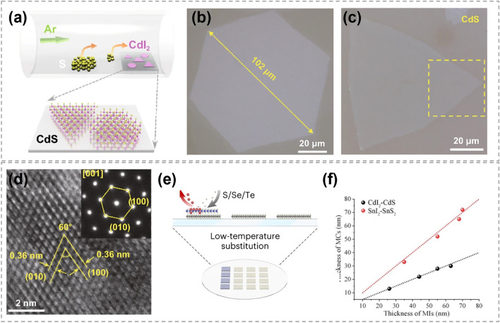
Owing to the low-energy-barrier substitution of iodine with other chalcogens, metal iodides are considered as promising reactants for atomic substitution to synthesize TMCs at low temperatures [34, 35]. It also shows a great advantage in growing non-layered TMCs (such as CdS) with an ultrathin thickness. For instance, using layered CdI2 nanosheets as host materials, Zhao et al. realized the synthesis of non-layered CdS nanosheets in a S rich vapor at 280–300 °C (Fig. 20a–d) [35]. The obtained CdS nanosheets possess a submillimeter size and atomic layer thickness of 2 nm, which was the smallest thickness as reported (marked in square region in Fig. 20c). Combining with DFT calculations, the formation process of CdS was proposed as follows: (i) replacement of I atoms by S atoms, (ii) formation of Cd–S chemical bonds, and (iii) lattice compression along the thickness-direction of CdS. In 2023, Zhang epitaxially grew metal iodide on wafer-scale substrates at a temperature below 400 °C, which was much lower than the direct growth of TMCs [34]. This metal iodide was then converted into TMCs by overcoming a small energy barrier of substitution between iodine and other chalcogens, as shown in Fig. 20e. By this two-step method, 17 different high-quality wafer scale TMCs (M = In, Cd, Cu, Co, Fe, Pb, Sn and Bi) were successfully synthesized, including metal sulfides, metal selenides, metal tellurides and metal chalcogenide alloys. Since most metal iodides are layered structures, during the transition to non-layered TMC crystals, the van der Waals gap between the iodide layers disappears, resulting in a reduction in the thickness of TMCs. As shown in Fig. 20f, the thickness of the obtained CdS sheet was almost half of that of the original CdI2 sheet. This method provides a new solution for the fabrication of ultrathin non-layered TMC materials with a large scale. Additionally, the substitutions involving transition metal iodide introduces a novel strategy for the synthesis of 2D TMCs synthesis at temperature below 400 °C.
Fig. 20.
Chalcogen substituting iodine in the synthesis of TMCs. a Schematic of the substitution and atomic structure of CdS flakes on mica substrate by chemical sulfurization method. b Representative optical microscope images of converted CdI2 thin flake on mica substrates. c Representative optical images of original large-scale CdI2 thin flake and converted CdS thin flake on mica substrates, respectively. d HRTEM image of converted CdS flakes. The inset is the selected area electron diffraction pattern taken along the direction [001] of CdS flakes. Reproduced with permission [35].
Copyright 2021, Springer Nature. e Schematic showing the preparation of CdS flakes on mica substrate by chemical sulfurization method. f The thickness of CdI2 and SnI2 flakes after being converted to CdS and SnS2. Reproduced with permission [34]. Copyright 2023, Springer Nature
Nitrogen-Chalcogen Substitution
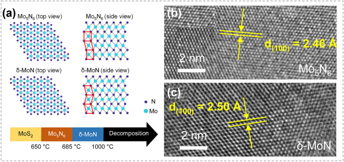
Through atomic substitution, layered 2D TMCs can also be converted into non-layered materials with an ultra-thin thickness. As illustrated in Fig. 21a, by using layered MoS2 as reactants, Ling et al. synthesized two phases of molybdenum nitride (Mo5N6 and δ-MoN) at different temperatures [165]. The morphology and 2D feature of host materials were inherited after the substitution of S with N, resulting in non-layered molybdenum nitrides. HRTEM image in Fig. 21b, c shows that the obtained Mo5N6 and δ-MoN were highly crystalline with a thickness of only a few nanometers. These obtained ultra-thin nitrides showed ohmic contacts with Cr/Au electrodes, indicating their promising applications in nanoelectronics.
Fig. 21.
Synthesis of nitrides by atomic substitution. a Crystal structures of Mo5N6 and δ-MoN. b, c HRTEM images of the obtained Mo5N6 and δ-MoN. Reproduced with permission [165].
Copyright 2022, American Chemical Society
Synthesis of 2D TMC Heterostructures
As one of the most important structures in semiconductor industry, heterostructures are essential in high-speed electronic and optoelectronic devices [166–169]. The majority of TMC heterostructures are composed of a series of materials in which either the transition metals or chalcogens are different. This allows for the exploration of different material combinations and properties [170–172]. Traditional preparation techniques for heterostructure refer to stitching or stacking different TMC components together via a direct growth procedure, such as CVD heteroepitaxial synthesis [173–175]. Generally, the designability of components and structures are restricted. In contrast, atomic substitution offers a powerful tool for precisely tailoring the interfaces and optimizing the performance of TMC heterostructures.
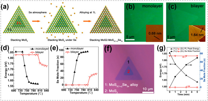
By performing layer-selected atomic substitution of MoS2 bilayer, Li et al. realized the synthesis of MoS2-MoS2(1-x)Se2x heterostructures [23]. Both the preparation of MoS2 bilayer and substitution process were performed by CVD, as shown in Fig. 22a–c. The substitution temperature for monolayer was 740 °C, while that for the bilayer was 810 °C (Fig. 22d–e). This makes it possible to control the substitution process by modulating the reaction temperature. Figure 22f shows that the achieved MoS2-MoS2(1-x)Se2x heterostructures were highly crystalline with a sharp interface. The photoluminescence energy and the corresponding Se composition of monolayer and bilayer regions at 750 °C as a function of annealing time is given in Fig. 22g. It was demonstrated that S atoms in the monolayer region underwent gradual substitution by Se atoms, whereas the bilayer region remained highly stable. Therefore, effective control over the temperature and duration of the substitution process allows for well-defined morphology of the synthesized heterostructure. These composition-tannable heterostructures hold great potentials in 2D fundamental physical research as well as the development of functional electronic and optoelectronic devices.
Fig. 22.
Heterostructure synthesized by chalcogenides substitution. a Schematic diagram of the preparation of MoS2-MoS2(1-x)Se2x heterostructure by the Se substitution in a designed stacking MoS2 nanosheet. b, c Optical images of monolayer and bilayer MoS2 nanosheets after substitution with the corresponding AFM images shown in inset. d, e Bandgap values and compositions of the two sheets as a function of annealing temperature. f, g Optical image, bandgap values and compositions of the obtained MoS2-MoS2(1-x)Se2x heterostructures. Reproduced with permission [23].
Copyright 2017, American Chemical Society
Patterned growth is a powerful method for customizing the morphology of heterostructures, which involves patterning the base material with a desired shape and a subsequent selective substitution. Figure 23a depicts the lithography process for the synthesis of lateral TMC heterostructures [176]. To realize selective substitution, a part of the MoSe2 film was protected by SiO2 mask. A MoSe2-MoS2 junction was achieved after well annealing in an S atmosphere. Figure 23b illustrates the optical image of the synthesized heterostructure, and Fig. 23c, d shows the Raman mapping intensity. In comparison, a uniform MoS2xSe2(1-x) alloy was obtained without protection by mask, and the substitution ratio ‘‘x’’ in MoS2xSe2(1-x) alloy could be tuned through controlling the extent of sulfurization. Based on this, alloyed heterostructures could be further synthesized by selectively sulfurizing MoS2xSe2(1-x) to MoS2xSe2(1-x)-MoS2ySe2(1-y) heterostructure, as illustrated in Fig. 23e. Similarly, Mahjouri-Samani et al. introduced an electron beam lithography method to selectively replace Se atoms in a mask-patterned MoSe2 flakes, and MoSe2-MoS2 heterojunction array was obtained under pulsed laser vaporization of sulfur [24]. Such lithography technology offers flexibility and benefits for both the precise device design and subsequent performance regulation. In 2021, Wang et al. realized the selective substitution by laser-induced oxidation without the assistance of masks [177]. As shown in Fig. 23f, monolayer MoS2 was synthesized via CVD and then scanned by a laser. The laser-scanned MoS2 could be oxidized into MoOx and then selenized in an Ar/H2 atmosphere (Fig. 23g). During selenization, the unoxidized region remained intact, because MoOx is easier to be selenized at a lower temperature as compared with MoS2.
Fig. 23.
The selective substitution of TMC heterostructure synthesis. a Schematic showing the heterostructures synthesis protocol based on the sulfurization of patterned MoSe2 monolayers. b Optical image of a representative lateral heterostructure. c, d Mapping intensity of the A1g Raman modes of MoSe2 in (b) at 241 cm–1 and MoS2 at 408 cm–1, respectively. e Schematic showing the realization of an (x, y)-heterostructure with x < y. Reproduced with permission [176].
Copyright 2020, American Chemical Society. f Schematic illustrations showing the formation process of MoS2-MoSe2 by laser patterning and selective selenization. g Microscopy images after the process illustrated in f. Reproduced with permission [177]. Copyright 2021, American Chemical Society
Metal oxide thin films were also used for the patterned synthesis of TMC heterostructures [178]. As illustrated in Fig. 24a, the MoOx thin film was deposited on the patterned region of SiO2/Si substrates with plasma enhanced atomic deposition, the obtained metal oxide was then sulfurized by thermal treatment. STEM and high-resolution scanning TEM images in Fig. 24b, c confirmed the realization of polycrystalline MoS2 films. Importantly, by using a designed MoOx/WOx heterostructure as the reactant, a lateral MoS2/WS2 heterostructures was obtained after sulfurization (Fig. 24d–f). This research provides an effective pathway for the synthesis of large-area 2D MaX2-MbX2 (Ma and Mb represent different metals) heterostructures.
Fig. 24.
Patterned synthesis of TMC by substituting oxygen atoms with chalcogens. a Scheme of the atomic layer deposition enabled growth of large area patterned MoS2. b STEM image showing the uniform coverage of the polycrystalline MoS2 film. The inset shows a selective area electron diffraction pattern from the same sample which confirms the polycrystalline. c HR-STEM image of MoS2. d-f Low magnification cross-sectional HR-STEM characterization of e WS2/MoS2 junction and magnified cross-sectional HR-STEM images of d WS2 and f MoS2 regions. Reproduced with permission [178].
Copyright 2020, IOP Publishing
Synthesis of 2D TMC Janus Structures
Janus structure stands out as a unique form of heterostructures, which is characterized by its asymmetric atomic arrangement [179]. The distinctive asymmetry gives rise to intriguing properties, including strong Rashba spin splitting, heightened second harmonic generation response, enhanced piezoelectric polarizations, as well as improved catalytic activity [180, 181]. Zhang et al. reported the synthesis of monolayer Janus SMoSe by selectively substituting Se atoms in the top layer of MoSe2 with S, as illustrated in Fig. 25a, b [182]. The S source, generated by heating sulfur powder to 150 °C, was introduced to react with MoSe2. The top Se layer of MoSe2 was exposed to the atmosphere and in direct contact with S atoms. As a result, Se atoms in the top Se layer underwent a rapid substitution by S atoms, while the bottom Se layer was maintained. It is worth noting that the substitution process was highly dependent on the experimental temperature (Fig. 25c). Within the temperature range of 750–850 °C, a Janus SMoSe monolayer with a 2H lattice structure was achieved (Fig. 25d). However, when the temperature exceeded 850 °C, the substitution extended to the bottom Se layer, which led to the formation of MoS2.
Fig. 25.
Synthesis of 2D TMC Janus structures by atomic substitution. Synthesis of 2D TMC Janus structures by atomic substitution. a Schematic illustration of the reaction setup for Janus SMoSe monolayer. b Different views of an eight-unit-cell Janus SMoSe monolayer. c Proposed mechanism for the sulfurization of monolayer MoSe2 at different temperatures. d HRTEM image of the Janus SMoSe lattice. Reproduced with permission [182].
Copyright 2017, American Chemical Society. e Schematic showing the asymmetric MoSSe monolayer structure. f Schematics showing key reaction steps for room-temperature atomic-layer substitution process. g Tilted ADF-STEM image of the Janus MoSSe sample. Reproduced with permission [156]. Copyright 2021, NATL ACAD SCIENCES
In 2021, Guo et al. proposed a room-temperature atomic-layer substitution method and synthesized Janus TMC structures successfully [156]. As illustrated in Fig. 25e, hydrogen plasma was applied to remove S atoms from the top S layer of a pre-grown MoS2, and Se vapor was supplied simultaneously to occupy the S vacancies. The detailed substitution process is schematically shown in Fig. 25f: (i) the initial state of MoS2, (ii) the adsorption and diffusion of two H atoms near a S atom, (iii) the formation of H2S, (iv) the desorption of H2S, and (v) the occupation of the vacancy site by Se atom. Annular dark-field STEM image in Fig. 25g confirmed the formation of the Janus structure, where Se atoms occupied one side of the monolayer SeMoS and S atoms occupied the other side.
Both of the above researches have realized the synthesis of Janus, though different methods adopted. The precious control of removing single-layer chalcogens is identified to be the crucial factor in both experiments. Compared with one-step synthesis method, post-treatment approach offers a better control over the morphology of the products. The synthesis of Janus structure opens up a new paradigm for the delicate design of artificial 2D materials, potentially unveiling unprecedented electronic, photonic and mechanical properties that are unexplored in nature.
Synthesis of 2D TMC Alloys
Without patterning or delicate control over experimental conditions, the partial substitution treatment of 2D TMC materials commonly results in 2D TMC alloys [183]. Li et al. have explored two strategies for the synthesis of monolayer MoS2xSe2(1-x) alloys by CVD methods [150], including the selenization of MoS2 and the sulfurization of MoSe2 (Fig. 26a, d). Optical images for MoS2 flakes before and after selenization are shown in Fig. 26b, c. It was found that S atoms were randomly and homogeneously substituted by Se, leading to the formation of a uniformly distributed MoS2xSe2(1-x) alloy. Optical images for MoSe2 flakes before and after sulfurization are shown in Fig. 26e, f. Different from the substitution of S by Se, the substitution of Se by S preferred to occur along specific crystalline orientations of MoSe2, leading to the synthesis of MoSe2/MoS2 bi-phases. The optical band gaps of obtained MoS2xSe2(1-x) alloys through the two different strategies were significantly different. Despite the selenization of transition metal disulfides presented a better control over the compositions and optical characteristics of monolayer TMC alloys, the different mechanisms of selenization and sulfurization are not clear.
Fig. 26.
Synthesis of TMC alloys by atomic substitution. a, d Schematic illustration of the experimental set-up for the selenization/sulfurization process. b, e Optical micrographs for the as-synthesized MoS2/MoSe2. c, f Selenized (sulfurized) MoS2/MoSe2 (at 800 °C) on sapphire substrates. Reproduced with permission [150].
Copyright 2014, Frontiers Media S.A. g Schematic setup for the post-growth substituting. h-j Atomically resolved ADF-STEM images showing the atomic structure of Te-doped MoS2 monolayer at different growth temperature. A number of bright sites corresponding to the local Te sites can be distinguished (marked with yellow circles). Scale bar: 1 nm. Reproduced with permission [151]. Copyright 2018, IOP Publishing. k Schematic illustration for the selenization process. l-n AFM images for the MoS2 flake l before and m after, n selenization at 800 °C. Reproduced with permission [184]. Copyright 2014, John Wiley and Sons
Additionally, the tellurization of MoS2 was also explored (Fig. 26g). At a relatively low Te concentration, Te replaced S randomly, resulting in the formation of a monolayer MoS2(1-x)Te2x alloy [151]. As the Te concentration increased to ~ 27.6%, local regions of Te enrichment accompanied with structure distortion were observed (Fig. 26h–j). Statistical analysis showed that Te substitution preferentially occurred in the top S sublattice of MoS2. Besides, hydrogen carrier gas played an indispensable role in the substitution process. In this research, the MoS2(1-x)Te2x alloys with composition controllable were realized by regulating the amount of the reactants. Similarly, Li et al. reported the synthesis of MoSxSey flakes through selenizing MoS2 monolayers (Fig. 26k) [184]. As the temperature increased, there was a gradual substitution of S atoms with Se. The atomic force microscope (AFM) images of MoS2 flakes before and after selenization are shown in Fig. 26l–n, which proved the intact crystal structure after selenization. The band gaps of the resulting MoSxSey alloys were effectively tuned from 1.86 to 1.57 eV, depending on the Se content. This study provides a brief and straightforward method for engineering the band gap of 2D TMCs. Nevertheless, to enhance control over the composition of TMC alloys, there is a substantial need for a comprehensive understanding on the relative mechanisms of the substitution processes among different chalcogens.
In addition to composition control, there is a strong demand for TMC materials with controllable morphology and domain size to further advance their applications. In Fig. 27, by tuning the temperature in physical vapor deposition (PVD) method, Feng et al. realized the synthesis of MoS2(1-x)Se2x (x = 0.41–1.00) monolayer alloys with controlled edge orientation (Mo-zigzag and S/Se-zigzag edge orientations) and domain size [185]. By maintaining lower temperature gradients in the deposition zone, MoS2(1-x)Se2x monolayer domains with size up to 20 μm were successfully obtained. This research provides valuable insights into the PVD growth of 2D TMC alloys, enabling control over composition, edge orientations as well as domain sizes.
Fig. 27.
Controllable synthesis of MoS2(1-x)Se2x alloys by atomic substitution. a Illustration of three-zone furnace setup for MoS2(1-x)Se2x (x = 0.41–1.00) monolayer growth. b-e SEM images of MoS0.78Se1.22 domains obtained at different deposition temperatures. f Schematic illustration of different morphologies at different temperatures. g Atomic structures showing domains obtained at different temperatures. Reproduced with permission [185].
Copyright 2015, American Chemical Society
It is worth noting that, by the atomic substitution methods, the obtained 0D and 1D MX alloys primarily belong to intermetallic alloys, while the achieved 2D MX2 alloys are classified as chalcogenide alloys. This may be attributed to the unique sandwich structure of MX2, where metal atoms are situated between two chalcogen layers, rendering the substitution between metal atoms more challenging.
Synthesis of 2D Doped TMC Materials
Compared to alloys, doping involves the addition of guest atoms with much lower concentrations. Generally, doping is focused on introducing specific properties or characteristics to the host material without significantly altering its structure. Transition metal doping is highly demanded for enriching the properties and applications of TMC materials [183, 186].
Recently, Chang et al. developed a two-step process for the doping of WS2 monolayer by Sn (Fig. 28a–c) [155]. Firstly, 2D WS2 monolayers were synthesized by conventional CVD. Secondly, a post-thermal doping process was conducted by annealing WS2 monolayers in a Sn-rich environment, which is produced by heating SnS precursors. HRTEM image in Fig. 28b confirmed that the high crystalline of WS2 monolayer was maintained after a small proportion of W atoms were substituted by Sn. Electrical measurements indicated that the WS2 after Sn doping showed n-type doping behaviors.
Fig. 28.
Metal atoms substitution doping of TMCs. a Schematic showing the thermal doping of Sn in WS2. b ADF-STEM images showing the area of Sn-doped WS2 monolayer. c Schematics showing the formation of Sn-doped WS2 monolayers. Reproduced with permission [155].
Copyright 2019, American Chemical Society. d-f ADF-STEM image, image simulation and atomic model from density functional theory (DFT) geometry optimization of the Co on Mo atop site. g-i HAADF image, image simulation from DFT geometry optimization and atomic model from geometry optimized DFT of a Co-substituted S site. j-l HAADF image, image simulation and atomic model from DFT geometry optimization showing Co in the hollow site. Reproduced with permission [154]. Copyright 2017, Springer Nature
Through a hydrothermal treatment of single-layer MoS2 by Co(thiourea)42+ complex, Tsang and co-workers realized isolated Co atom doping in MoS2 [154]. The loading of Co in monolayer MoS2 was 1.8 wt%. As shown in Fig. 28d–l, isolated Co atoms incorporated into MoS2 basal plane showed three configurations: Co locating on atop site of Mo, Co substituting S site, and Co locating in the hollow site. Simulation results showed that Co atoms located on atop site of Mo atoms were the most energetically favorable. In another case recently reported by this group, the doping content of Co was raised to 3.0 wt% by increasing the Co/Mo ratio in the mixed solution in hydrothermal method [187]. This method can be applied to various transition metals, such as Fe, Co, Ni, Ru, Pd, and Ag, as mentioned in their study. It is noted that Dolui et al. employed ab initio calculations to explore various dopants at substitution and adsorption sites in monolayer MoS2 [183]. Nb, Zr, and Y atoms were found to act as p-type dopants and prefer to substitute the Mo lattice sites, since they had a lower number of valence electrons than Mo. These researches provide new strategies for the structural modification of 2D TMCs by atom doping and lays a foundation for the rational design of 2D TMCs to satisfy various requirements.
Chalcogen doping has also been extensively explored. Ma et al. employed a conventional CVD technique to grow monolayer MoS2, followed by the selective removal of a certain proportion of sulfur atoms by Ar plasma [188]. Diselenodiphenyl was then used to perform Se doping in MoS2 crystals. The photoluminescence spectra in Fig. 29a showed evidence for the successful doping of Se atoms, and the composition-based band gap modulation was consistent with theoretical predictions. Combining this method with patterning, it is possible to realize doping at desired locations. Se-doped MoS2 nanosheets could also be synthesized by annealing MoS2 with diphenyl diselenide at 800 °C (Fig. 29b) [189, 190]. The Se contents after substitution was approximately 6%. It's worth noting that there was an expansion of the interlayer spacing from 0.6 to 0.88 nm after such a small Se doping, implying an increase in the degree of disorder (Fig. 29c, d), which resulted in an increase in the number of active edge sites and therefore an improved catalytic activity [189]. These research results show that introducing doping to modulate chemical composition provides routes to improve the electronic, optical and chemical properties of TMCs.
Fig. 29.
Chalcogens substitution doping in TMCs. a Normalized room-temperature photoluminescence spectra of a single-layer MoS2 film after sputtering and diselenodiphenyl insertion cycles. Reproduced with permission [188].
Copyright 2014, American Chemical Society. b Schematic illustration of the synthesis procedure for the Se-doped MoS2 nanosheets. c HRTEM image and (inset) the corresponding selected area electron diffraction patterns of Se-doped MoS2 nanosheets. d The lattice distances of the labeled green and red lines in c. Reproduced with permission [189]. Copyright 2015, The Royal Society of Chemistry. (Color figure online)
In addition to metals and chalcogens, other elements have also been explored as dopants to regulate the electrical properties of TMCs, such as H [21, 191], O [192, 193], Cl [194], N [195], P [196], etc. In Fig. 30a, Kim et al. proposed a strategy of site-selective P doping in ultrathin MoS2 through laser-assisted reaction [197]. This method could realize the precise control of doping both temporally and spatially. In Fig. 30b–d, Liang et al. explored oxygen induced controllable p-type doping in a series of 2D TMCs such as MoTe2, WSe2, MoSe2, PtSe2 and PdSe2 [198]. Three possible mechanisms for promoting p-type doping in 2D TMCs were proposed: charge transfer from absorbed oxygen molecules, formation of surface oxide and substitution of sulfur atoms. Peto et al. investigated the process of oxygen substitution to S in MoS2 (Fig. 30e, f) [199]. O atoms were found to spontaneously and slowly bind with the basal plane to replace S atoms one by one. The oxygen substitution sites on MoS2 surface could act as the single atom reaction centers, greatly improving the catalytic activity for the electrochemical hydrogen evolution reaction. This study provides new ways for engineering 2D TMC electrocatalysts with single O-atom active sites. Yang et al. proposed a simple and convenient way to realize Cl-doping in mechanically exfoliated few-layer (3.5–5 nm) WS2 and MoS2 [194]. In this method, TMC flakes were soaked in undiluted 1,2-dichloroethane at room temperature for more than 12 h. Figure 30g shows the schematic of the structure of Cl-doped WS2 (MoS2) back gate field-effect transistors (FETs). The observed negative threshold voltage shift for WS2 FETs after 1,2-dichloroethane treatment proved the n-doping effect (Fig. 30h, i). It was also found that the contact resistance was reduced after doping, which was beneficial for improving the performance of 2D nano electron-device.
Fig. 30.
Nonmetal elements substitution doping in TMCs. a Schematic diagram of the laser-assisted doping method. Reproduced with permission [197].
Copyright 2016, John Wiley and Sons. b Illustration showing charge transfer from oxygen molecules. c Isoelectronic substitution of chalcogen atoms in TMCs. d Illustration showing charge transfer from oxide. Reproduced with permission [198]. Copyright 2020, Springer Nature. e Schematic representation of atmospheric oxygen atoms getting adsorbed on a MoS2 monolayer. f Scanning tunneling microscope image of O atoms (bright spots) absorbed at S vacancies (dark triangles) sites. Reproduced with permission [199]. Copyright 2018, Springer Nature. g Schematic of Cl-doped few-layer WS2 back-gate field-effect transistors (FETs). h Transfer characteristics of the device (Cl-doped). The Ion/Ioff ratio is about 4 × 10⁶ and 3 × 10⁷ at Vds of 2 and 0.05 V, respectively. i Transfer characteristics of the device (undoped). The Ion/Ioff ratio is about 2 × 10⁶ and 1.1 × 10⁴ at Vds of 2 and 0.05 V. Reproduced with permission [194]. Copyright 2014, American Chemical Society. j IDS-VGS characteristics of multilayer nitrogen-doped MoS2 FET. Reproduced with permission [195]. Copyright 2016, American Chemical Society
Doping TMCs by N and P elements has been achieved by using post-growth treatments including NH3 plasma treatment [200], N2 plasma treatment [195, 201], annealing in NH3 [202], and PH3 plasma treatment [196]. Azcatl et al. found that the threshold voltage of the transfer curve of MoS2 FETs shows a positive shift after N2 plasma treatment, indicating that N substitution doping induced the p-type doping effect (Fig. 30j) [195]. Nipane et al. also reported that p-type doping could be achieved in few-layer MoS2 by PH3/He plasma treatment [196].
In this section, the applications of atomic substitution strategy in 2D TMCs were reviewed. Different from the synthesis of 0D and 1D TMCs that occurs in solutions, atomic substitution approaches employed in 2D TMCs typically take place in a vapor atmosphere. To date, various 2D TMCs with desired compositions and morphologies, such as binary compounds, heterostructures, Janus, and alloys, have been realized by precious control on temperature, reaction time and chemical environment of the substitution process. It is worth noting that this strategy also makes it possible to synthesis 2D TMC structures at low temperatures by choosing appropriate reactants. However, the exploration in the controllable synthesis is most concentrated on the experiments. The understanding of substitution mechanisms between various atoms, particularly those involving different chalcogens, remains unclear. Hence, there is a need to provide a systematic theoretical analysis of the substitution process, grounded in the mechanisms underlying these various substitution categories.
3D Materials
Additionally, the atomic substitution method also exhibits considerable potential in the synthesis of 3D materials. In Fig. 31a, Li et al. [203] prepared mixed HFAxMA1-xPbI3Cl (MA = methylammonium, FA = formamidinium) perovskite precursor films, using stoichiometric [HCl + (1 − x)MAI + x FAI + PbI2] solutions, and realized a structural conversion from 2 to 3D. The designed HFAxMA1-xPbI3Cl perovskite film, without long chain spacing, is inherently instable, which provides possibilities for H/FA(MA) and Cl/I ion exchange reactions. During the reactions, the exchanged H+ and Cl− formed highly volatile HCl, readily releasing into the air. Meanwhile, the layer-structured 2D PbI2 precursor was transformed into a 3D structure, leading to the production of a phase-pure and high-quality 3D FAxMA1-xPbI3 perovskite. This research provides an effective and facile method for the synthesis of phase-pure halide perovskite with mixed-composition.
Fig. 31.
Atomic substitution in 3D materials. a Schematic diagram showing the transformation of 2D mixed HFAxMA1-xPbI3Cl into 3D FAxMA1-xPbI3 (MA = methylammonium, FA = formamidinium). Reproduced with permission [203].
Copyright 2016, John Wiley and Sons. b Illustration showing the preparation of compositionally graded mixed-cation lead mix-halide perovskite absorbers. Reproduced with permission [204]. Copyright 2018, John Wiley and Sons. c, d Atomic structure and optical images of MAPbBr3/MAPbI3 heterostructures. Reproduced with permission [205]. Copyright 2016, American Chemical Society. e MA-mediation synthesis of FA1−xMAxPbI3 mixed-organic-cation iodide perovskite from MA+-excess precursor solutions. X− denotes an anion that does not conform with the structure. Reproduced with permission [206]. Copyright 2017, John Wiley and Sons
By the partial anion exchange method, Fu et al. [204] prepared compositionally graded perovskite absorbers successfully. As illustrated in Fig. 31b, MAPbI3 was prepared first as the starting absorber. It was then treated by spin coating MABr solution at room temperature to induce halide ion-exchange, and finally the MABr-treated film was thermally annealed under a chlorobenzene vapor atmosphere to promote the diffusion and redistribution of ions. Consequently, a MAPbI3-xBrx perovskite absorber with a compositionally graded layer was formed, featuring a continuous decrease in Br concentration throughout the entire thickness. This achieved perovskite absorbers show an improve of the photovoltaic performance and operational stability in near-infrared-transparent perovskite solar cells. Except for the synthesis of compositional grading structures, the partial exchange method can also facilitate the fabrication of heterostructures. Shewmon et al. [205] achieved MAPbBr3/MAPbI3 heterojunctions by immersing MAPbBr3 single crystals into a MAPbI3 solution (Fig. 31c, d). The newly formed MAPbI3 layers were shown to be single crystalline, with the exchange of halide ions dominating the formation process. This work paves the way for the future research on optoelectronic devices using single-crystal materials.
Apart from anions substitution reactions, cations exchange can also occur in 3D materials. For instance, Li et al. [206] synthesized FA1−xMAxPbI3 mixed-organic-cation iodide perovskite (MOCP) thin films by adding excess MA+ cations into the precursor solution. As illustrated in Fig. 31e, FA+, MA+, X− and PbI2 were random and disordered in the precursor solution, here X− anion must be not incompatible with the MOCP crystalline structure in order to avoid influencing the composition of the final MOCP. At the room temperature, MOCPs with a relatively large fraction of MA+ cations were formed (Stage I). With the following thermal-annealing step, ion-exchange reactions occurred between pre-formed MOCPs and the surrounding FA+ (Stage II), due to FA+-rich hybrid organic–inorganic perovskites are thermodynamically more stable at increased temperatures. With the depletion of FA+ cations outside the MOCP phases, phase-pure, uniform and precisely composed MOCPs were formed (Stage III). During the process, the composition of the as-formed MOCPs is dynamically tuned with the FA+/MA+ ratio. In summary, the atomic substitution method provides a possible strategy for the synthesis of intricate 3D materials with diverse compositions and morphologies.
Conclusion and Prospect
In recent years, the atomic substitution method has emerged as a prominent technique for the fabrication and manipulation for low-dimensional TMC materials due to its capacity for precise control over morphologies, compositions and structures. So far, extensive research efforts have been conducted to understand the underlying mechanisms of atomic substitution. It has been revealed that defects in the host materials play a crucial role in initiating the substitution reaction. Various experimental factors, including the chemical environment, temperature, and crystal structure, have been identified as significant factors in the process of atomic substitution. Additionally, the structures and morphologies of the resulting materials are greatly influenced by the substituting elements, substitution ratios, and substitution positions. Based on the understanding on the fundamental mechanisms of atomic substitute, a large variety of high-quality low-dimensional TMC materials have been successfully synthesized. Nevertheless, delicate control for atomic substitution, especially in the case of 2D TMCs, is still in its early stages.
To achieve the ultimate goal of realizing TMC materials with well-defined structures and compositions, more efforts are still required: (i) In situ characterizations are highly demanded for providing valuable insights into atomic substitution. By employing in-situ techniques such as STEM, X-ray photoelectron spectroscopy, Raman, Fourier transform Infrared spectroscopy, and X-ray absorption spectra, the dynamic transformation and reconstruction of active sites can be effectively visualized, allowing for a comprehensive understanding on the nature of a typical reaction [207]. (ii) The close collaboration between theoretical studies and experiments is encouraged. Theoretical studies are indispensable for understanding the synthesis mechanisms of materials [208, 209], and further providing guidelines for controllable synthesis. We believe that with the close collaboration between theoretical studies and experiments, theories of atomic substitution will finally be established and controllable synthesis of TMC materials will be realized. Besides, the diversity of types and combinations within TMC materials results in a vast number of members within this family. This intricate nature presents a challenge in fully exploring TMC materials by experiments, in this case, high-throughput computing research will be quite helpful.
Atomic substitution offers advantages not only in precisely engineering and customizing the desired properties of TMC materials but also in potentially overcoming the limitations of direct synthesis methods. However, it should be noted that although atomic substitution has been successfully achieved in laboratory, there is still a significant gap toward its practical implementation. With a comprehensive understanding of the mechanisms behind atomic substitution, it is anticipated that various synthesis procedures will be further optimized in the near future, and simultaneously, large-scale production will be achieved.
Acknowledgements
This work was supported by the Teli Fellowship from Beijing Institute of Technology, the National Natural Science Foundation of China (Nos. 52303366, 22173109). The Analysis and Testing Center in Beijing Institute of Technology was also acknowledged.
Declarations
Conflict of interest
The authors declare that they have no known competing financial interests or personal relationships that could have appeared to influence the work reported in this paper.
Footnotes
Xuan Wang and Akang Chen have contributed equally to this work.
Contributor Information
Jiatao Zhang, Email: zhangjt@bit.edu.cn.
Jichen Dong, Email: dongjichen@iccas.ac.cn.
Leining Zhang, Email: leiningzhang@bit.edu.cn.
References
- 1.X.-Y. Yu, L. Yu, X.W.D. Lou, Metal sulfide hollow nanostructures for electrochemical energy storage. Adv. Energy Mater. 6, 1501333 (2016). 10.1002/aenm.201501333 [Google Scholar]
- 2.X. Rui, H. Tan, Q. Yan, Nanostructured metal sulfides for energy storage. Nanoscale 6, 9889–9924 (2014). 10.1039/c4nr03057e [DOI] [PubMed] [Google Scholar]
- 3.X. Huang, Z. Zeng, H. Zhang, Metal dichalcogenide nanosheets: preparation, properties and applications. Chem. Soc. Rev. 42, 1934–1946 (2013). 10.1039/C2CS35387C [DOI] [PubMed] [Google Scholar]
- 4.M. Chhowalla, Z. Liu, H. Zhang, Two-dimensional transition metal dichalcogenide (TMD) nanosheets. Chem. Soc. Rev. 44, 2584–2586 (2015). 10.1039/C5CS90037A [DOI] [PubMed] [Google Scholar]
- 5.S.-C. Zhu, S. Li, B. Tang, H. Liang, B.-J. Liu et al., MXene-motivated accelerated charge transfer over TMCs quantum dots for solar-powered photoreduction catalysis. J. Catal. 404, 56–66 (2021). 10.1016/j.jcat.2021.09.001 [Google Scholar]
- 6.H. Jin, M. Ahn, S. Jeong, J.H. Han, D. Yoo et al., Colloidal single-layer quantum dots with lateral confinement effects on 2D exciton. J. Am. Chem. Soc. 138, 13253–13259 (2016). 10.1021/jacs.6b06972 [DOI] [PubMed] [Google Scholar]
- 7.S.-C. Zhu, F.-X. Xiao, Transition metal chalcogenides quantum dots: emerging building blocks toward solar-to-hydrogen conversion. ACS Catal. 13, 7269–7309 (2023). 10.1021/acscatal.2c05401 [Google Scholar]
- 8.P. Wang, D. Yang, X. Pi, Toward wafer-scale production of 2D transition metal chalcogenides. Adv. Electron. Mater. 7, 2100278 (2021). 10.1002/aelm.202100278 [Google Scholar]
- 9.L. Zhang, J. Dong, F. Ding, Strategies, status, and challenges in wafer scale single crystalline two-dimensional materials synthesis. Chem. Rev. 121, 6321–6372 (2021). 10.1021/acs.chemrev.0c01191 [DOI] [PubMed] [Google Scholar]
- 10.P. Adel, A. Wolf, T. Kodanek, D. Dorfs, Segmented CdSe@CdS/ZnS nanorods synthesized via a partial ion exchange sequence. Chem. Mater. 26, 3121–3127 (2014). 10.1021/cm500431m [Google Scholar]
- 11.Y. Shemesh, J.E. MacDonald, G. Menagen, U. Banin, Synthesis and photocatalytic properties of a family of CdS-PdX hybrid nanoparticles. Angew. Chem. Int. Ed. Engl. 50, 1185–1189 (2011). 10.1002/anie.201006407 [DOI] [PubMed] [Google Scholar]
- 12.S. Li, J. Hong, B. Gao, Y.C. Lin, H.E. Lim et al., Tunable doping of rhenium and vanadium into transition metal dichalcogenides for two-dimensional electronics. Adv. Sci. 8, e2004438 (2021). 10.1002/advs.202004438 [DOI] [PMC free article] [PubMed] [Google Scholar]
- 13.Y.H. Lee, X.Q. Zhang, W. Zhang, M.T. Chang, C.T. Lin et al., Synthesis of large-area MoS2 atomic layers with chemical vapor deposition. Adv. Mater. 24, 2320–2325 (2012). 10.1002/adma.201104798 [DOI] [PubMed] [Google Scholar]
- 14.Q. Fu, L. Yang, W. Wang, A. Han, J. Huang et al., Synthesis and enhanced electrochemical catalytic performance of monolayer WS2(1–x)Se2x with a tunable band gap. Adv. Mater. 27, 4732–4738 (2015). 10.1002/adma.201500368 [DOI] [PubMed] [Google Scholar]
- 15.J. Wang, X. Xu, T. Cheng, L. Gu, R. Qiao et al., Dual-coupling-guided epitaxial growth of wafer-scale single-crystal WS2 monolayer on vicinal a-plane sapphire. Nat. Nanotechnol. 17, 33–38 (2022). 10.1038/s41565-021-01004-0 [DOI] [PubMed] [Google Scholar]
- 16.J. Tan, S. Li, B. Liu, H.-M. Cheng, Structure, preparation, and applications of 2D material-based metal–semiconductor heterostructures. Small Struct. 2, 2170001 (2021). 10.1002/sstr.202170001 [Google Scholar]
- 17.X. Zhang, L. Huangfu, Z. Gu, S. Xiao, J. Zhou et al., Controllable epitaxial growth of large-area MoS2/WS2 vertical heterostructures by confined-space chemical vapor deposition. Small 17, e2007312 (2021). 10.1002/smll.202007312 [DOI] [PubMed] [Google Scholar]
- 18.Y. Li, J. Liu, X. Li, X. Wan, R. Pan et al., Evolution of hollow CuInS2 nanododecahedrons via kirkendall effect driven by cation exchange for efficient solar water splitting. ACS Appl. Mater. Interfaces 11, 27170–27177 (2019). 10.1021/acsami.9b05325 [DOI] [PubMed] [Google Scholar]
- 19.T. Afaneh, P.K. Sahoo, I.A.P. Nobrega, Y. Xin, H.R. Gutiérrez, Laser-assisted chemical modification of monolayer transition metal dichalcogenides. Adv. Funct. Mater. 28, 1802949 (2018). 10.1002/adfm.201802949 [Google Scholar]
- 20.Y. Qin, M. Sayyad, A.R.-P. Montblanch, M.S.G. Feuer, D. Dey et al., Reaching the excitonic limit in 2D Janus monolayers by in situ deterministic growth. Adv. Mater. 34, e2106222 (2022). 10.1002/adma.202106222 [DOI] [PubMed] [Google Scholar]
- 21.A.-Y. Lu, H. Zhu, J. Xiao, C.-P. Chuu, Y. Han et al., Janus monolayers of transition metal dichalcogenides. Nat. Nanotechnol. 12, 744–749 (2017). 10.1038/nnano.2017.100 [DOI] [PubMed] [Google Scholar]
- 22.B. Kirubasankar, Y.S. Won, L.A. Adofo, S.H. Choi, S.M. Kim et al., Atomic and structural modifications of two-dimensional transition metal dichalcogenides for various advanced applications. Chem. Sci. 13, 7707–7738 (2022). 10.1039/d2sc01398c [DOI] [PMC free article] [PubMed] [Google Scholar]
- 23.H. Li, X. Wu, H. Liu, B. Zheng, Q. Zhang et al., Composition-modulated two-dimensional semiconductor lateral heterostructures via layer-selected atomic substitution. ACS Nano 11, 961–967 (2017). 10.1021/acsnano.6b07580 [DOI] [PubMed] [Google Scholar]
- 24.M. Mahjouri-Samani, M.-W. Lin, K. Wang, A.R. Lupini, J. Lee et al., Patterned arrays of lateral heterojunctions within monolayer two-dimensional semiconductors. Nat. Commun. 6, 7749 (2015). 10.1038/ncomms8749 [DOI] [PMC free article] [PubMed] [Google Scholar]
- 25.J.L. Fenton, B.C. Steimle, R.E. Schaak, Tunable intraparticle frameworks for creating complex heterostructured nanoparticle libraries. Science 360, 513–517 (2018). 10.1126/science.aar5597 [DOI] [PubMed] [Google Scholar]
- 26.T. Zhang, K. Fujisawa, F. Zhang, M. Liu, M.C. Lucking et al., Universal In situ substitutional doping of transition metal dichalcogenides by liquid-phase precursor-assisted synthesis. ACS Nano 14, 4326–4335 (2020). 10.1021/acsnano.9b09857 [DOI] [PubMed] [Google Scholar]
- 27.H. Chen, Z. Chen, B. Ge, Z. Chi, H. Chen et al., General strategy for two-dimensional transition metal dichalcogenides by ion exchange. Chem. Mater. 29, 10019–10026 (2017). 10.1021/acs.chemmater.7b03523 [Google Scholar]
- 28.C.-S. Tan, C.-H. Hsiao, S.-C. Wang, P.-H. Liu, M.-Y. Lu et al., Sequential cation exchange generated superlattice nanowires forming multiple p-n heterojunctions. ACS Nano 8, 9422–9426 (2014). 10.1021/nn5035247 [DOI] [PubMed] [Google Scholar]
- 29.K. Lambert, B. De Geyter, I. Moreels, Z. Hens, PbTe|CdTe core|shell particles by cation exchange, a HR-TEM study. Chem. Mater. 21, 778–780 (2009). 10.1021/cm8029399 [Google Scholar]
- 30.P. Zhou, F. Lv, N. Li, Y. Zhang, Z. Mu et al., Strengthening reactive metal-support interaction to stabilize high-density Pt single atoms on electron-deficient g-C3N4 for boosting photocatalytic H2 production. Nano Energy 56, 127–137 (2019). 10.1016/j.nanoen.2018.11.033 [Google Scholar]
- 31.D.-H. Ha, A.H. Caldwell, M.J. Ward, S. Honrao, K. Mathew et al., Solid-solid phase transformations induced through cation exchange and strain in 2D heterostructured copper sulfide nanocrystals. Nano Lett. 14, 7090–7099 (2014). 10.1021/nl5035607 [DOI] [PubMed] [Google Scholar]
- 32.A.P. Tiwari, D. Kim, Y. Kim, O. Prakash, H. Lee, Highly active and stable layered ternary transition metal chalcogenide for hydrogen evolution reaction. Nano Energy 28, 366–372 (2016). 10.1016/j.nanoen.2016.08.065 [Google Scholar]
- 33.S. Dogan, S. Kudera, Z. Dang, F. Palazon, U. Petralanda et al., Lateral epitaxial heterojunctions in single nanowires fabricated by masked cation exchange. Nat. Commun. 9, 505 (2018). 10.1038/s41467-018-02878-w [DOI] [PMC free article] [PubMed] [Google Scholar]
- 34.K. Zhang, Y. She, X. Cai, M. Zhao, Z. Liu et al., Epitaxial substitution of metal iodides for low-temperature growth of two-dimensional metal chalcogenides. Nat. Nanotechnol. 18, 448–455 (2023). 10.1038/s41565-023-01326-1 [DOI] [PubMed] [Google Scholar]
- 35.M. Zhao, S. Yang, K. Zhang, L. Zhang, P. Chen et al., A universal atomic substitution conversion strategy towards synthesis of large-size ultrathin nonlayered two-dimensional materials. Nano-Micro Lett. 13, 165 (2021). 10.1007/s40820-021-00692-6 [DOI] [PMC free article] [PubMed] [Google Scholar]
- 36.Z. Yuan, Z. Hu, I. Persson, C. Wang, X. Liu et al., Interface-assisted cation exchange enables high-performance perovskiteLEDs with tunable near-infrared emissions. Joule 6, 2423–2436 (2022). 10.1016/j.joule.2022.08.003 [Google Scholar]
- 37.A. Chen, X. Li, J. Wang, J. Zhang, Colloidal synthesis of semiconductor films for efficient photoelectrochemical hydrogen generation. Energy Mater. Adv. 4, 28 (2023). 10.34133/energymatadv.0028 [Google Scholar]
- 38.Z. Li, M. Saruyama, T. Asaka, Y. Tatetsu, T. Teranishi, Determinants of crystal structure transformation of ionic nanocrystals in cation exchange reactions. Science 373, 332–337 (2021). 10.1126/science.abh2741 [DOI] [PubMed] [Google Scholar]
- 39.G.D. Moon, S. Ko, Y. Xia, U. Jeong, Chemical transformations in ultrathin chalcogenide nanowires. ACS Nano 4, 2307–2319 (2010). 10.1021/nn9018575 [DOI] [PubMed] [Google Scholar]
- 40.G. Gariano, V. Lesnyak, R. Brescia, G. Bertoni, Z. Dang et al., Role of the crystal structure in cation exchange reactions involving colloidal Cu2Se nanocrystals. J. Am. Chem. Soc. 139, 9583–9590 (2017). 10.1021/jacs.7b03706 [DOI] [PMC free article] [PubMed] [Google Scholar]
- 41.E. Groeneveld, L. Witteman, M. Lefferts, X. Ke, S. Bals et al., Tailoring ZnSe-CdSe colloidal quantum dots via cation exchange: from core/shell to alloy nanocrystals. ACS Nano 7, 7913–7930 (2013). 10.1021/nn402931y [DOI] [PubMed] [Google Scholar]
- 42.R. Tu, Y. Xie, G. Bertoni, A. Lak, R. Gaspari et al., Influence of the ion coordination number on cation exchange reactions with copper telluride nanocrystals. J. Am. Chem. Soc. 138, 7082–7090 (2016). 10.1021/jacs.6b02830 [DOI] [PMC free article] [PubMed] [Google Scholar]
- 43.X. Yan, X.-Y. Fu, F.-X. Xiao, Filling the gap: atomically precise metal nanoclusters-induced Z-scheme photosystem toward robust and stable solar hydrogen generation. Adv. Funct. Mater. 33, 2303737 (2023). 10.1002/adfm.202303737 [Google Scholar]
- 44.B.L. Li, M.I. Setyawati, H.L. Zou, J.X. Dong, H.Q. Luo et al., Emerging 0D transition-metal dichalcogenides for sensors, biomedicine, and clean energy. Small 13, 201700527 (2017). 10.1002/smll.201700527 [DOI] [PubMed] [Google Scholar]
- 45.A.L. Morris, C. Lin, S.E. Benjamin, V.V.N.M. Devarasetty, W.R. Tilluck et al., Toward improved scalability of cation exchange reactions of metal chalcogenide nanocrystals. Chem. Mater. 29, 6596–6600 (2017). 10.1021/acs.chemmater.7b01065 [Google Scholar]
- 46.H. Li, K. Wu, J. Lim, H.-J. Song, V.I. Klimov, Doctor-blade deposition of quantum dots onto standard window glass for low-loss large-area luminescent solar concentrators. Nat. Energy 1, 16157 (2016). 10.1038/nenergy.2016.157 [Google Scholar]
- 47.K. Wu, H. Li, V.I. Klimov, Tandem luminescent solar concentrators based on engineered quantum dots. Nat. Photonics 12, 105–110 (2018). 10.1038/s41566-017-0070-7 [Google Scholar]
- 48.J. Liu, J. Feng, J. Gui, T. Chen, M. Xu et al., Metal@semiconductor core-shell nanocrystals with atomically organized interfaces for efficient hot electron-mediated photocatalysis. Nano Energy 48, 44–52 (2018). 10.1016/j.nanoen.2018.02.040 [Google Scholar]
- 49.Q. Yuan, D. Liu, N. Zhang, W. Ye, H. Ju et al., Noble-metal-free janus-like structures by cation exchange for Z-scheme photocatalytic water splitting under broadband light irradiation. Angew. Chem. Int. Ed. 56, 4206–4210 (2017). 10.1002/anie.201700150 [DOI] [PubMed] [Google Scholar]
- 50.L. Zhu, M. Gao, C.K.N. Peh, G.W. Ho, Solar-driven photothermal nanostructured materials designs and prerequisites for evaporation and catalysis applications. Mater. Horiz. 5, 323–343 (2018). 10.1039/C7MH01064H [Google Scholar]
- 51.M. Ji, M. Xu, W. Zhang, Z. Yang, L. Huang et al., Structurally well-defined Au@Cu2-xS core-shell nanocrystals for improved cancer treatment based on enhanced photothermal efficiency. Adv. Mater. 28, 3094–3101 (2016). 10.1002/adma.201503201 [DOI] [PubMed] [Google Scholar]
- 52.A.M. Salaheldin, J. Walter, P. Herre, I. Levchuk, Y. Jabbari et al., Automated synthesis of quantum dot nanocrystals by hot injection: mixing induced self-focusing. Chem. Eng. J. 320, 232–243 (2017). 10.1016/j.cej.2017.02.154 [Google Scholar]
- 53.K. De Nolf, R.K. Capek, S. Abe, M. Sluydts, Y. Jang et al., Controlling the size of hot injection made nanocrystals by manipulating the diffusion coefficient of the solute. J. Am. Chem. Soc. 137, 2495–2505 (2015). 10.1021/ja509941g [DOI] [PubMed] [Google Scholar]
- 54.J. Zhang, Y. Tang, K. Lee, M. Ouyang, Tailoring light-matter-spin interactions in colloidal hetero-nanostructures. Nature 466, 91–95 (2010). 10.1038/nature09150 [DOI] [PubMed] [Google Scholar]
- 55.L. He, C. Luan, S. Liu, M. Chen, N. Rowell et al., Transformations of magic-size clusters via precursor compound cation exchange at room temperature. J. Am. Chem. Soc. 144, 19060–19069 (2022). 10.1021/jacs.2c07972 [DOI] [PubMed] [Google Scholar]
- 56.J. Feng, J. Liu, X. Cheng, J. Liu, M. Xu et al., Hydrothermal cation exchange enabled gradual evolution of Au@ZnS-AgAuS yolk-shell nanocrystals and their visible light photocatalytic applications. Adv. Sci. 5, 1700376 (2017). 10.1002/advs.201700376 [DOI] [PMC free article] [PubMed] [Google Scholar]
- 57.L. Peng, Y. Wang, Q. Dong, Z. Wang, Passivated ZnSe nanocrystals prepared by hydrothermal methods and their optical properties. Nano-Micro Lett. 2, 190–196 (2010). 10.1007/bf03353640 [Google Scholar]
- 58.T. Avellini, N. Soni, N. Silvestri, S. Fiorito, F. De Donato et al., Cation exchange protocols to radiolabel aqueous stabilized ZnS, ZnSe, and CuFeS2 nanocrystals with 64Cu for dual radio- and photo-thermal therapy. Adv. Funct. Mater. 30, 2002362 (2020). 10.1002/adfm.202002362 [DOI] [PMC free article] [PubMed] [Google Scholar]
- 59.A.E. Powell, J.M. Hodges, R.E. Schaak, Preserving both anion and cation sublattice features during a nanocrystal cation-exchange reaction: synthesis of metastable wurtzite-type CoS and MnS. J. Am. Chem. Soc. 138, 471–474 (2016). 10.1021/jacs.5b10624 [DOI] [PubMed] [Google Scholar]
- 60.Y. Feng, Y. Ji, Y. Zhang, Q. Shao, Y. Xu et al., Synthesis of noble metal chalcogenides via cation exchange reactions. Nat. Synth. 1, 626–634 (2022). 10.1038/s44160-022-00117-1 [Google Scholar]
- 61.D.H. Son, S.M. Hughes, Y. Yin, A. Paul, Alivisatos Cation exchange reactions in ionic nanocrystals. Science 306, 1009–1012 (2004). 10.1126/science.1103755 [DOI] [PubMed] [Google Scholar]
- 62.B.J. Beberwyck, Y. Surendranath, A.P. Alivisatos, Cation exchange: a versatile tool for nanomaterials synthesis. J. Phys. Chem. C 117, 19759–19770 (2013). 10.1021/jp405989z [Google Scholar]
- 63.L. De Trizio, L. Manna, Forging colloidal nanostructures via cation exchange reactions. Chem. Rev. 116, 10852–10887 (2016). 10.1021/acs.chemrev.5b00739 [DOI] [PMC free article] [PubMed] [Google Scholar]
- 64.R.G. Pearson, Absolute electronegativity and hardness: application to inorganic chemistry. Inorg. Chem. 27, 734–740 (1988). 10.1021/ic00277a030 [Google Scholar]
- 65.J. Gui, M. Ji, J. Liu, M. Xu, J. Zhang et al., Phosphine-initiated cation exchange for precisely tailoring composition and properties of semiconductor nanostructures: old concept, new applications. Angew. Chem. Int. Ed. 54, 3683–3687 (2015). 10.1002/anie.201410053 [DOI] [PubMed] [Google Scholar]
- 66.B. Bai, M. Xu, N. Li, W. Chen, J. Liu et al., Semiconductor nanocrystal engineering by applying thiol- and solvent-coordinated cation exchange kinetics. Angew. Chem. Int. Ed. 58, 4852–4857 (2019). 10.1002/anie.201807695 [DOI] [PubMed] [Google Scholar]
- 67.B. Bai, C. Zhao, M. Xu, J. Ma, Y. Du et al., Unique cation exchange in nanocrystal matrix via surface vacancy engineering overcoming chemical kinetic energy barriers. Chem 6, 3086–3099 (2020). 10.1016/j.chempr.2020.08.020 [Google Scholar]
- 68.L. Chen, Z. Kong, H. Tao, H. Hu, J. Gao et al., Crystal structure dependent cation exchange reactions in Cu2-xS nanoparticles. Nanoscale 14, 3907–3916 (2022). 10.1039/d1nr08077f [DOI] [PubMed] [Google Scholar]
- 69.J. Zhang, Y. Tang, K. Lee, M. Ouyang, Nonepitaxial growth of hybrid core-shell nanostructures with large lattice mismatches. Science 327, 1634–1638 (2010). 10.1126/science.1184769 [DOI] [PubMed] [Google Scholar]
- 70.Q. Zhao, M. Ji, H. Qian, B. Dai, L. Weng et al., Controlling structural symmetry of a hybrid nanostructure and its effect on efficient photocatalytic hydrogen evolution. Adv. Mater. 26, 1387–1392 (2014). 10.1002/adma.201304652 [DOI] [PubMed] [Google Scholar]
- 71.X. Wan, Y. Pan, Y. Xu, J. Liu, H. Chen et al., Ultralong lifetime of plasmon-excited electrons realized in nonepitaxial/epitaxial Au@CdS/CsPbBr 3 triple-heteronanocrystals. Adv. Mater. 35, e2207555 (2023). 10.1002/adma.202207555 [DOI] [PubMed] [Google Scholar]
- 72.S. Gupta, S.V. Kershaw, A.L. Rogach, 25th anniversary article: ion exchange in colloidal nanocrystals. Adv. Mater. 25, 6923–6943 (2013). 10.1002/adma.201302400 [DOI] [PubMed] [Google Scholar]
- 73.W.-Y. Wu, S. Chakrabortty, A. Guchhait, G.Y.Z. Wong, G.K. Dalapati et al., Solution-processed 2D PbS nanoplates with residual Cu2S exhibiting low resistivity and high infrared responsivity. Chem. Mater. 28, 9132–9138 (2016). 10.1021/acs.chemmater.6b04330 [Google Scholar]
- 74.M. Dalmases, P. Torruella, J. Blanco-Portals, A. Vidal, M. Lopez-Haro et al., Gradual transformation of Ag2S to Au2S nanoparticles by sequential cation exchange reactions: binary, ternary, and hybrid compositions. Chem. Mater. 30, 6893–6902 (2018). 10.1021/acs.chemmater.8b03208 [Google Scholar]
- 75.L. De Trizio, H. Li, A. Casu, A. Genovese, A. Sathya et al., Sn cation valency dependence in cation exchange reactions involving Cu2-xSe nanocrystals. J. Am. Chem. Soc. 136, 16277–16284 (2014). 10.1021/ja508161c [DOI] [PMC free article] [PubMed] [Google Scholar]
- 76.Y. Liu, M. Liu, M.T. Swihart, Shape evolution of biconcave djurleite Cu1.94S nanoplatelets produced from CuInS2 nanoplatelets by cation exchange. J. Am. Chem. Soc. 139, 18598–18606 (2017). 10.1021/jacs.7b09577 [DOI] [PubMed] [Google Scholar]
- 77.J.M.R. Tan, M.C. Scott, W. Hao, T. Baikie, C.T. Nelson et al., Revealing cation-exchange-induced phase transformations in multielemental chalcogenide nanoparticles. Chem. Mater. 29, 9192–9199 (2017). 10.1021/acs.chemmater.7b03029 [Google Scholar]
- 78.A.C. Berends, W. van der Stam, Q.A. Akkerman, J.D. Meeldijk, J. van der Lit et al., Anisotropic 2D Cu2-xSe nanocrystals from dodecaneselenol and their conversion to CdSe and CuInSe2 nanoparticles. Chem. Mater. 30, 3836–3846 (2018). 10.1021/acs.chemmater.8b01143 [DOI] [PMC free article] [PubMed] [Google Scholar]
- 79.B.C. Steimle, A.M. Fagan, A.G. Butterfield, R.W. Lord, C.R. McCormick et al., Experimental insights into partial cation exchange reactions for synthesizing heterostructured metal sulfide nanocrystals. Chem. Mater. 32, 5461–5482 (2020). 10.1021/acs.chemmater.0c01388 [Google Scholar]
- 80.A.G. Butterfield, C.R. McCormick, J.M. Veglak, R.E. Schaak, Morphology-dependent phase selectivity of cobalt sulfide during nanoparticle cation exchange reactions. J. Am. Chem. Soc. 143, 7915–7919 (2021). 10.1021/jacs.1c03478 [DOI] [PubMed] [Google Scholar]
- 81.X. Li, M. Ji, H. Li, H. Wang, M. Xu et al., Cation/anion exchange reactions toward the syntheses of upgraded nanostructures: principles and applications. Matter 2, 554–586 (2020). 10.1016/j.matt.2019.12.024 [Google Scholar]
- 82.H. Jin, C. Livache, W.D. Kim, B.T. Diroll, R.D. Schaller et al., Spin-exchange carrier multiplication in manganese-doped colloidal quantum dots. Nat. Mater. 22, 1013–1021 (2023). 10.1038/s41563-023-01598-x [DOI] [PMC free article] [PubMed] [Google Scholar]
- 83.M. Casavola, M.A. van Huis, S. Bals, K. Lambert, Z. Hens et al., Anisotropic cation exchange in PbSe/CdSe core/shell nanocrystals of different geometry. Chem. Mater. 24, 294–302 (2012). 10.1021/cm202796s [Google Scholar]
- 84.M.V. Kovalenko, R.D. Schaller, D. Jarzab, M.A. Loi, D.V. Talapin, Inorganically functionalized PbS-CdS colloidal nanocrystals: integration into amorphous chalcogenide glass and luminescent properties. J. Am. Chem. Soc. 134, 2457–2460 (2012). 10.1021/ja2087689 [DOI] [PubMed] [Google Scholar]
- 85.Y. Justo, B. Goris, J.S. Kamal, P. Geiregat, S. Bals et al., Multiple dot-in-rod PbS/CdS heterostructures with high photoluminescence quantum yield in the near-infrared. J. Am. Chem. Soc. 134, 5484–5487 (2012). 10.1021/ja300337d [DOI] [PubMed] [Google Scholar]
- 86.L. Li, T.J. Daou, I. Texier, T.T. Kim Chi, N.Q. Liem et al., Highly luminescent CuInS2/ZnS core/shell nanocrystals: cadmium-free quantum dots for in vivo imaging. Chem. Mater. 21, 2422–2429 (2009). 10.1021/cm900103b [Google Scholar]
- 87.D.V. Talapin, J.H. Nelson, E.V. Shevchenko, S. Aloni, B. Sadtler et al., Seeded growth of highly luminescent CdSe/CdS nanoheterostructures with rod and tetrapod morphologies. Nano Lett. 7, 2951–2959 (2007). 10.1021/nl072003g [DOI] [PubMed] [Google Scholar]
- 88.C.L. Choi, K.J. Koski, S. Sivasankar, A.P. Alivisatos, Strain-dependent photoluminescence behavior of CdSe/CdS nanocrystals with spherical, linear, and branched topologies. Nano Lett. 9, 3544–3549 (2009). 10.1021/nl9017572 [DOI] [PMC free article] [PubMed] [Google Scholar]
- 89.A.M. Smith, A.M. Mohs, S. Nie, Tuning the optical and electronic properties of colloidal nanocrystals by lattice strain. Nat. Nanotechnol. 4, 56–63 (2009). 10.1038/nnano.2008.360 [DOI] [PMC free article] [PubMed] [Google Scholar]
- 90.K. Yu, B. Zaman, S. Romanova, D.-S. Wang, J.A. Ripmeester, Sequential synthesis of type II colloidal CdTe/CdSe core-shell nanocrystals. Small 1, 332–338 (2005). 10.1002/smll.200400069 [DOI] [PubMed] [Google Scholar]
- 91.P.T. Chin, C.D. Donega, S.S. van Bavel, S.C. Meskers, N.A. Sommerdijk et al., Highly luminescent CdTe/CdSe colloidal heteronanocrystals with temperature-dependent emission color. J. Am. Chem. Soc. 129, 14880–14886 (2007). 10.1021/ja0738071 [DOI] [PubMed] [Google Scholar]
- 92.E. Zhang, J. Liu, M. Ji, H. Wang, X. Wan et al., Hollow anisotropic semiconductor nanoprisms with highly crystalline frameworks for high-efficiency photoelectrochemical water splitting. J. Mater. Chem. A 7, 8061–8072 (2019). 10.1039/C9TA00925F [Google Scholar]
- 93.H. Wang, Y. Gao, J. Liu, X. Li, M. Ji et al., Efficient plasmonic Au/CdSe nanodumbbell for photoelectrochemical hydrogen generation beyond visible region. Adv. Energy Mater. 9, 1803889 (2019). 10.1002/aenm.201803889 [Google Scholar]
- 94.X. Li, M.A. Iqbal, M. Xu, Y.-C. Wang, H. Wang et al., Au@HgxCd1-xTe core@shell nanorods by sequential aqueous cation exchange for near-infrared photodetectors. Nano Energy 57, 57–65 (2019). 10.1016/j.nanoen.2018.12.030 [Google Scholar]
- 95.X. Wan, Y. Gao, M. Eshete, M. Hu, R. Pan et al., Simultaneous harnessing of hot electrons and hot holes achieved via n-metal-p Janus plasmonic heteronanocrystals. Nano Energy 98, 107217 (2022). 10.1016/j.nanoen.2022.107217 [Google Scholar]
- 96.M. Saruyama, Y.-G. So, K. Kimoto, S. Taguchi, Y. Kanemitsu et al., Spontaneous formation of wurzite-CdS/zinc blende-CdTe heterodimers through a partial anion exchange reaction. J. Am. Chem. Soc. 133, 17598–17601 (2011). 10.1021/ja2078224 [DOI] [PubMed] [Google Scholar]
- 97.Y. Lim, C.-H. Lee, C.-H. Jun, K. Kim, J. Cheon, Morphology-conserving non-kirkendall anion exchange of metal oxide nanocrystals. J. Am. Chem. Soc. 142, 9130–9134 (2020). 10.1021/jacs.0c03230 [DOI] [PubMed] [Google Scholar]
- 98.B. Jia, W. Zhao, D. Sun, L. Fan, H. Yao et al., Robust anion exchange realized in crystalline metal cyanamide nanoparticles. Chem. Mater. 31, 9532–9539 (2019). 10.1021/acs.chemmater.9b03934 [Google Scholar]
- 99.K. Miszta, D. Dorfs, A. Genovese, M.R. Kim, L. Manna, Cation exchange reactions in colloidal branched nanocrystals. ACS Nano 5, 7176–7183 (2011). 10.1021/nn201988w [DOI] [PubMed] [Google Scholar]
- 100.J. Liu, Q. Zhao, J.-L. Liu, Y.-S. Wu, Y. Cheng et al., Heterovalent-doping-enabled efficient dopant luminescence and controllable electronic impurity via a new strategy of preparing II-VI nanocrystals. Adv. Mater. 27, 2753–2761 (2015). 10.1002/adma.201500247 [DOI] [PubMed] [Google Scholar]
- 101.K. Miszta, G. Gariano, R. Brescia, S. Marras, F. De Donato et al., Selective cation exchange in the core region of Cu2-xSe/Cu2-xS core/shell nanocrystals. J. Am. Chem. Soc. 137, 12195–12198 (2015). 10.1021/jacs.5b06379 [DOI] [PMC free article] [PubMed] [Google Scholar]
- 102.W. Huang, M. Xu, J. Liu, J. Wang, Y. Zhu et al., Hydrophilic doped quantum dots “ink” and their inkjet-printed patterns for dual mode anticounterfeiting by reversible cation exchange mechanism. Adv. Funct. Mater. 29, 1808762 (2019). 10.1002/adfm.201808762 [Google Scholar]
- 103.B. Bai, M. Xu, J. Li, S. Zhang, C. Qiao et al., Dopant diffusion equilibrium overcoming impurity loss of doped QDs for multimode anti-counterfeiting and encryption. Adv. Funct. Mater. 31, 2100286 (2021). 10.1002/adfm.202100286 [Google Scholar]
- 104.A. Gupta, J.C. Ondry, M. Chen, M.H. Hudson, I. Coropceanu et al., Diffusion-limited kinetics of isovalent cation exchange in III-V nanocrystals dispersed in molten salt reaction media. Nano Lett. 22, 6545–6552 (2022). 10.1021/acs.nanolett.2c01699 [DOI] [PMC free article] [PubMed] [Google Scholar]
- 105.L. Cheng, S. Shen, S. Shi, Y. Yi, X. Wang et al., FeSe2-decorated Bi2Se3 nanosheets fabricated via cation exchange for Chelator-free 64Cu-labeling and multimodal image-guided photothermal-radiation therapy. Adv. Funct. Mater. 26, 2185–2197 (2016). 10.1002/adfm.201504810 [DOI] [PMC free article] [PubMed] [Google Scholar]
- 106.J. Song, C. Ma, W. Zhang, X. Li, W. Zhang et al., Bandgap and structure engineering via cation exchange: from binary Ag2S to ternary AgInS2, quaternary AgZnInS alloy and AgZnInS/ZnS core/shell fluorescent nanocrystals for bioimaging. ACS Appl. Mater. Interfaces 8, 24826–24836 (2016). 10.1021/acsami.6b07768 [DOI] [PubMed] [Google Scholar]
- 107.R. Zeng, K. Lian, B. Su, L. Lu, J. Lin et al., Versatile synthesis of hollow metal sulfides via reverse cation exchange reactions for photocatalytic CO2 reduction. Angew. Chem. Int. Ed. 60, 25055–25062 (2021). 10.1002/anie.202110670 [DOI] [PubMed] [Google Scholar]
- 108.J. Lim, Y.-S. Park, V.I. Klimov, Optical gain in colloidal quantum dots achieved with direct-current electrical pumping. Nat. Mater. 17, 42–49 (2018). 10.1038/nmat5011 [DOI] [PubMed] [Google Scholar]
- 109.Y.-S. Park, J. Lim, V.I. Klimov, Asymmetrically strained quantum dots with non-fluctuating single-dot emission spectra and subthermal room-temperature linewidths. Nat. Mater. 18, 249–255 (2019). 10.1038/s41563-018-0254-7 [DOI] [PubMed] [Google Scholar]
- 110.H. Li, M. Zanella, A. Genovese, M. Povia, A. Falqui et al., Sequential cation exchange in nanocrystals: preservation of crystal phase and formation of metastable phases. Nano Lett. 11, 4964–4970 (2011). 10.1021/nl202927a [DOI] [PubMed] [Google Scholar]
- 111.S.E. Creutz, R. Fainblat, Y. Kim, M.C. De Siena, D.R. Gamelin, A selective cation exchange strategy for the synthesis of colloidal Yb3+-doped chalcogenide nanocrystals with strong broadband visible absorption and long-lived near-infrared emission. J. Am. Chem. Soc. 139, 11814–11824 (2017). 10.1021/jacs.7b04938 [DOI] [PubMed] [Google Scholar]
- 112.A.R. Freyer, P.C. Sercel, Z. Hou, B.H. Savitzky, L.F. Kourkoutis et al., Explaining the unusual photoluminescence of semiconductor nanocrystals doped via cation exchange. Nano Lett. 19, 4797–4803 (2019). 10.1021/acs.nanolett.9b02284 [DOI] [PubMed] [Google Scholar]
- 113.Z.-Q. Zhou, L.-Y. Yang, R. Yan, J. Zhao, Y.-Q. Liu et al., Mn-Doped ZnSe quantum dots initiated mild and rapid cation exchange for tailoring the composition and optical properties of colloid nanocrystals: novel template, new applications. Nanoscale 9, 2824–2835 (2017). 10.1039/c6nr09094j [DOI] [PubMed] [Google Scholar]
- 114.H. Shao, C. Wang, S. Xu, Y. Jiang, Y. Shao et al., Hydrazine-promoted sequential cation exchange: a novel synthesis method for doped ternary semiconductor nanocrystals with tunable emission. Nanotechnology 25, 025603 (2014). 10.1088/0957-4484/25/2/025603 [DOI] [PubMed] [Google Scholar]
- 115.V. Lesnyak, C. George, A. Genovese, M. Prato, A. Casu et al., Alloyed copper chalcogenide nanoplatelets via partial cation exchange reactions. ACS Nano 8, 8407–8418 (2014). 10.1021/nn502906z [DOI] [PMC free article] [PubMed] [Google Scholar]
- 116.Y. Li, J. Liu, X. Wan, R. Pan, B. Bai et al., Surface passivation enabled-structural engineering of I-III-VI2 nanocrystal photocatalysts. J. Mater. Chem. A 8, 9951–9962 (2020). 10.1039/D0TA01501F [Google Scholar]
- 117.W. Zhu, Z. Lin, X. Zhang, W. Wang, Y. Li, Room-temperature formation of alloy ZnxCd13-xSe13 magic-size clusters via cation exchange in diamine solution. Nanoscale 14, 11210–11217 (2022). 10.1039/d2nr02399g [DOI] [PubMed] [Google Scholar]
- 118.A. Bora, J. Lox, R. Hübner, N. Weiß, H. Bahmani Jalali et al., Composition-dependent optical properties of Cu–Zn–In–Se colloidal nanocrystals synthesized via cation exchange. Chem. Mater. 35, 4068–4077 (2023). 10.1021/acs.chemmater.3c00538 [Google Scholar]
- 119.H. Doh, S. Hwang, S. Kim, Size-tunable synthesis of nearly monodisperse Ag2S nanoparticles and size-dependent fate of the crystal structures upon cation exchange to AgInS2 nanoparticles. Chem. Mater. 28, 8123–8127 (2016). 10.1021/acs.chemmater.6b04011 [Google Scholar]
- 120.X. Cheng, J. Liu, J. Feng, E. Zhang, H. Wang et al., Metal@I2–II–IV–VI4 core–shell nanocrystals: controlled synthesis by aqueous cation exchange for efficient photoelectrochemical hydrogen generation. J. Mater. Chem. A 6, 11898–11908 (2018). 10.1039/C8TA03070G [Google Scholar]
- 121.J. Liu, J. Zhang, Nanointerface chemistry: lattice-mismatch-directed synthesis and application of hybrid nanocrystals. Chem. Rev. 120, 2123–2170 (2020). 10.1021/acs.chemrev.9b00443 [DOI] [PubMed] [Google Scholar]
- 122.R.E. Schaak, B.C. Steimle, J.L. Fenton, Made-to-order heterostructured nanoparticle libraries. Acc. Chem. Res. 53, 2558–2568 (2020). 10.1021/acs.accounts.0c00520 [DOI] [PubMed] [Google Scholar]
- 123.J.M. Pietryga, D.J. Werder, D.J. Williams, J.L. Casson, R.D. Schaller et al., Utilizing the lability of lead selenide to produce heterostructured nanocrystals with bright, stable infrared emission. J. Am. Chem. Soc. 130, 4879–4885 (2008). 10.1021/ja710437r [DOI] [PubMed] [Google Scholar]
- 124.Q. Lin, N.S. Makarov, W.-K. Koh, K.A. Velizhanin, C.M. Cirloganu et al., Design and synthesis of heterostructured quantum dots with dual emission in the visible and infrared. ACS Nano 9, 539–547 (2015). 10.1021/nn505793y [DOI] [PubMed] [Google Scholar]
- 125.I. Rosina, B. Martín-García, D. Spirito, Z. Dang, G. Gariano et al., Metastable CdTe@HgTe Core@Shell nanostructures obtained by partial cation exchange evolve into sintered CdTe films upon annealing. Chem. Mater. 32, 2978–2985 (2020). 10.1021/acs.chemmater.9b05281 [DOI] [PMC free article] [PubMed] [Google Scholar]
- 126.G.A. Di Domizio, L.T. Alameda, J. Fanghanel, R.W. Lord, J.R. Miller et al., Real-time monitoring of competing nanoparticle formation pathways during cation exchange using benchtop light scattering. Chem. Mater. 33, 3936–3944 (2021). 10.1021/acs.chemmater.0c04938 [Google Scholar]
- 127.J.L. Fenton, R.E. Schaak, Structure-selective cation exchange in the synthesis of zincblende MnS and CoS nanocrystals. Angew. Chem. Int. Ed. 56, 6464–6467 (2017). 10.1002/anie.201701087 [DOI] [PubMed] [Google Scholar]
- 128.D. Yin, Q. Li, Y. Liu, M.T. Swihart, Anion exchange induced formation of kesterite copper zinc tin sulphide-copper zinc tin selenide nanoheterostructures. Nanoscale 13, 4828–4834 (2021). 10.1039/d0nr08991e [DOI] [PubMed] [Google Scholar]
- 129.D. Zhang, A.B. Wong, Y. Yu, S. Brittman, J. Sun et al., Phase-selective cation-exchange chemistry in sulfide nanowire systems. J. Am. Chem. Soc. 136, 17430–17433 (2014). 10.1021/ja511010q [DOI] [PubMed] [Google Scholar]
- 130.D.O. Demchenko, R.D. Robinson, B. Sadtler, C.K. Erdonmez, A.P. Alivisatos et al., Formation mechanism and properties of CdS-Ag2S nanorod superlattices. ACS Nano 2, 627–636 (2008). 10.1021/nn700381y [DOI] [PubMed] [Google Scholar]
- 131.R.D. Robinson, B. Sadtler, D.O. Demchenko, C.K. Erdonmez, L.W. Wang et al., Spontaneous superlattice formation in nanorods through partial cation exchange. Science 317, 355–358 (2007). 10.1126/science.1142593 [DOI] [PubMed] [Google Scholar]
- 132.J.M. Luther, H. Zheng, B. Sadtler, A.P. Alivisatos, Synthesis of PbS nanorods and other ionic nanocrystals of complex morphology by sequential cation exchange reactions. J. Am. Chem. Soc. 131, 16851–16857 (2009). 10.1021/ja906503w [DOI] [PubMed] [Google Scholar]
- 133.B. Sadtler, D.O. Demchenko, H. Zheng, S.M. Hughes, M.G. Merkle et al., Selective facet reactivity during cation exchange in cadmium sulfide nanorods. J. Am. Chem. Soc. 131, 5285–5293 (2009). 10.1021/ja809854q [DOI] [PubMed] [Google Scholar]
- 134.D. Lee, W.D. Kim, S. Lee, W.K. Bae, S. Lee et al., Direct Cd-to-Pb exchange of CdSe nanorods into PbSe/CdSe axial heterojunction nanorods. Chem. Mater. 27, 5295–5304 (2015). 10.1021/acs.chemmater.5b01548 [Google Scholar]
- 135.J. Zhang, B.D. Chernomordik, R.W. Crisp, D.M. Kroupa, J.M. Luther et al., Preparation of Cd/Pb chalcogenide heterostructured Janus particles via controllable cation exchange. ACS Nano 9, 7151–7163 (2015). 10.1021/acsnano.5b01859 [DOI] [PubMed] [Google Scholar]
- 136.Y. Sim, A. Yoon, H.S. Kang, J. Kwak, S.-Y. Kim et al., Design of 2D layered catalyst by coherent heteroepitaxial conversion for robust hydrogen generation. Adv. Funct. Mater. 31, 2005449 (2021). 10.1002/adfm.202005449 [Google Scholar]
- 137.H. Lin, Z. Zhang, H. Zhang, K.T. Lin, X. Wen et al., Engineering van der waals materials for advanced metaphotonics. Chem. Rev. 122, 15204–15355 (2022). 10.1021/acs.chemrev.2c00048 [DOI] [PubMed] [Google Scholar]
- 138.Y. Zhang, Y. Yao, M.G. Sendeku, L. Yin, X. Zhan et al., Recent progress in CVD growth of 2D transition metal dichalcogenides and related heterostructures. Adv. Mater. 31, e1901694 (2019). 10.1002/adma.201901694 [DOI] [PubMed] [Google Scholar]
- 139.T. Chowdhury, E.C. Sadler, T.J. Kempa, Progress and prospects in transition-metal dichalcogenide research beyond 2D. Chem. Rev. 120, 12563–12591 (2020). 10.1021/acs.chemrev.0c00505 [DOI] [PubMed] [Google Scholar]
- 140.Z. Hu, Z. Wu, C. Han, J. He, Z. Ni et al., Two-dimensional transition metal dichalcogenides: interface and defect engineering. Chem. Soc. Rev. 47, 3100–3128 (2018). 10.1039/C8CS00024G [DOI] [PubMed] [Google Scholar]
- 141.M. Xu, T. Liang, M. Shi, H. Chen, Graphene-like two-dimensional materials. Chem. Rev. 113, 3766–3798 (2013). 10.1021/cr300263a [DOI] [PubMed] [Google Scholar]
- 142.F.A. Rasmussen, K.S. Thygesen, Computational 2D materials database: electronic structure of transition-metal dichalcogenides and oxides. J. Phys. Chem. C 119, 13169–13183 (2015). 10.1021/acs.jpcc.5b02950 [Google Scholar]
- 143.Z. Fei, T. Palomaki, S. Wu, W. Zhao, X. Cai et al., Edge conduction in monolayer WTe2. Nat. Phys. 13, 677–682 (2017). 10.1038/nphys4091 [Google Scholar]
- 144.S. Tang, C. Zhang, D. Wong, Z. Pedramrazi, H.-Z. Tsai et al., Quantum spin Hall state in monolayer 1T’-WTe2. Nat. Phys. 13, 683–687 (2017). 10.1038/nphys4174 [Google Scholar]
- 145.S. Wu, V. Fatemi, Q.D. Gibson, K. Watanabe, T. Taniguchi et al., Observation of the quantum spin Hall effect up to 100 kelvin in a monolayer crystal. Science 359, 76–79 (2018). 10.1126/science.aan6003 [DOI] [PubMed] [Google Scholar]
- 146.W. Choi, N. Choudhary, G.H. Han, J. Park, D. Akinwande et al., Recent development of two-dimensional transition metal dichalcogenides and their applications. Mater. Today 20, 116–130 (2017). 10.1016/j.mattod.2016.10.002 [Google Scholar]
- 147.B. Radisavljevic, A. Radenovic, J. Brivio, V. Giacometti, A. Kis, Single-layer MoS2 transistors. Nat. Nanotechnol. 6, 147–150 (2011). 10.1038/nnano.2010.279 [DOI] [PubMed] [Google Scholar]
- 148.G.-B. Liu, D. Xiao, Y. Yao, X. Xu, W. Yao, Electronic structures and theoretical modelling of two-dimensional group-VIB transition metal dichalcogenides. Chem. Soc. Rev. 44, 2643–2663 (2015). 10.1039/c4cs00301b [DOI] [PubMed] [Google Scholar]
- 149.X. Xu, W. Yao, D. Xiao, T.F. Heinz, Spin and pseudospins in layered transition metal dichalcogenides. Nat. Phys. 10, 343–350 (2014). 10.1038/nphys2942 [Google Scholar]
- 150.S.-H. Su, W.-T. Hsu, C.-L. Hsu, C.-H. Chen, M.-H. Chiu et al., Controllable synthesis of band-gap-tunable and monolayer transition-metal dichalcogenide alloys. Front. Energy Res. 2, 27 (2014). 10.3389/fenrg.2014.00027 [Google Scholar]
- 151.G. Yin, D. Zhu, D. Lv, A. Hashemi, Z. Fei et al., Hydrogen-assisted post-growth substitution of tellurium into molybdenum disulfide monolayers with tunable compositions. Nanotechnology 29, 145603 (2018). 10.1088/1361-6528/aaabe8 [DOI] [PubMed] [Google Scholar]
- 152.Z. Liu, S. Feng, X. Cai, H. Liu, J. Li et al., Large-size superlattices synthesized by sequential sulfur substitution-induced transformation of metastable MoTe2. Chem. Mater. 33, 9760–9768 (2021). 10.1021/acs.chemmater.1c03663 [Google Scholar]
- 153.H. Taghinejad, D.A. Rehn, C. Muccianti, A.A. Eftekhar, M. Tian et al., Defect-mediated alloying of monolayer transition-metal dichalcogenides. ACS Nano 12, 12795–12804 (2018). 10.1021/acsnano.8b07920 [DOI] [PubMed] [Google Scholar]
- 154.G. Liu, A.W. Robertson, M.M. Li, W.C.H. Kuo, M.T. Darby et al., MoS2 monolayer catalyst doped with isolated Co atoms for the hydrodeoxygenation reaction. Nat. Chem. 9, 810–816 (2017). 10.1038/nchem.2740 [DOI] [PubMed] [Google Scholar]
- 155.R.J. Chang, Y. Sheng, G.H. Ryu, N. Mkhize, T. Chen et al., Postgrowth substitutional tin doping of 2D WS2 crystals using chemical vapor deposition. ACS Appl. Mater. Interfaces 11, 24279–24288 (2019). 10.1021/acsami.9b06588 [DOI] [PubMed] [Google Scholar]
- 156.Y. Guo, Y. Lin, K. Xie, B. Yuan, J. Zhu et al., Designing artificial two-dimensional landscapes via atomic-layer substitution. Proc. Natl. Acad. Sci. U.S.A. 118, e2106124118 (2021). 10.1073/pnas.2106124118 [DOI] [PMC free article] [PubMed] [Google Scholar]
- 157.C. Zhu, M. Yu, J. Zhou, Y. He, Q. Zeng et al., Strain-driven growth of ultra-long two-dimensional nano-channels. Nat. Commun. 11, 772 (2020). 10.1038/s41467-020-14521-8 [DOI] [PMC free article] [PubMed] [Google Scholar]
- 158.S.J. Yun, G.H. Han, H. Kim, D.L. Duong, B.G. Shin et al., Telluriding monolayer MoS2 and WS2 via alkali metal scooter. Nat. Commun. 8, 2163 (2017). 10.1038/s41467-017-02238-0 [DOI] [PMC free article] [PubMed] [Google Scholar]
- 159.K. Bogaert, S. Liu, J. Chesin, D. Titow, S. Gradečak et al., Diffusion-mediated synthesis of MoS2/WS2 lateral heterostructures. Nano Lett. 16, 5129–5134 (2016). 10.1021/acs.nanolett.6b02057 [DOI] [PubMed] [Google Scholar]
- 160.Y.-Z. Chen, H. Medina, T.-Y. Su, J.-G. Li, K.-Y. Cheng et al., Ultrafast and low temperature synthesis of highly crystalline and patternable few-layers tungsten diselenide by laser irradiation assisted selenization process. ACS Nano 9, 4346–4353 (2015). 10.1021/acsnano.5b00866 [DOI] [PubMed] [Google Scholar]
- 161.M.A. Bissett, A.G. Hattle, A.J. Marsden, I.A. Kinloch, R.A.W. Dryfe, Enhanced photoluminescence of solution-exfoliated transition metal dichalcogenides by laser etching. ACS Omega 2, 738–745 (2017). 10.1021/acsomega.6b00294 [DOI] [PMC free article] [PubMed] [Google Scholar]
- 162.A. Castellanos-Gomez, M. Barkelid, A.M. Goossens, V.E. Calado, H.S.J. van der Zant et al., Laser-thinning of MoS2: on demand generation of a single-layer semiconductor. Nano Lett. 12, 3187–3192 (2012). 10.1021/nl301164v [DOI] [PubMed] [Google Scholar]
- 163.J. Lu, A. Carvalho, X.K. Chan, H. Liu, B. Liu et al., Atomic healing of defects in transition metal dichalcogenides. Nano Lett. 15, 3524–3532 (2015). 10.1021/acs.nanolett.5b00952 [DOI] [PubMed] [Google Scholar]
- 164.P. Browning, S. Eichfeld, K. Zhang, L. Hossain, Y.-C. Lin et al., Large-area synthesis of WSe 2 from WO 3 by selenium–oxygen ion exchange. 2D Mater. 2, 014003 (2015). 10.1088/2053-1583/2/1/014003 [Google Scholar]
- 165.H. Gao, J. Cao, T. Li, W. Luo, M. Gray et al., Phase-controllable synthesis of ultrathin molybdenum nitride crystals via atomic substitution of MoS2. Chem. Mater. 34, 351–357 (2022). 10.1021/acs.chemmater.1c03712 [Google Scholar]
- 166.Y. Gong, J. Lin, X. Wang, G. Shi, S. Lei et al., Vertical and in-plane heterostructures from WS2/MoS2 monolayers. Nat. Mater. 13, 1135–1142 (2014). 10.1038/nmat4091 [DOI] [PubMed] [Google Scholar]
- 167.R. Dong, I. Kuljanishvili, Review Article: progress in fabrication of transition metal dichalcogenides heterostructure systems. J Vac Sci Technol B Nanotechnol Microelectron 35, 030803 (2017). 10.1116/1.4982736 [DOI] [PMC free article] [PubMed] [Google Scholar]
- 168.B. Amin, N. Singh, U. Schwingenschlögl, Heterostructures of transition metal dichalcogenides. Phys. Rev. B 92, 075439 (2015). 10.1103/physrevb.92.075439 [Google Scholar]
- 169.C. Tan, H. Zhang, Two-dimensional transition metal dichalcogenide nanosheet-based composites. Chem. Soc. Rev. 44, 2713–2731 (2015). 10.1039/C4CS00182F [DOI] [PubMed] [Google Scholar]
- 170.Y. Liu, N.O. Weiss, X. Duan, H.-C. Cheng, Y. Huang et al., Van der Waals heterostructures and devices. Nat. Rev. Mater. 1, 16042 (2016). 10.1038/natrevmats.2016.42 [Google Scholar]
- 171.A.K. Geim, I.V. Grigorieva, Van der waals heterostructures. Nature 499, 419–425 (2013). 10.1038/nature12385 [DOI] [PubMed] [Google Scholar]
- 172.K.F. Mak, J. Shan, Photonics and optoelectronics of 2D semiconductor transition metal dichalcogenides. Nat. Photonics 10, 216–226 (2016). 10.1038/nphoton.2015.282 [Google Scholar]
- 173.J. Zhou, B. Tang, J. Lin, D. Lv, J. Shi et al., Morphology engineering in monolayer MoS2-WS2 lateral heterostructures. Adv. Funct. Mater. 28, 1801568 (2018). 10.1002/adfm.201801568 [Google Scholar]
- 174.Z. Wang, Y. Xie, H. Wang, R. Wu, T. Nan et al., NaCl-assisted one-step growth of MoS2-WS2 in-plane heterostructures. Nanotechnology 28, 325602 (2017). 10.1088/1361-6528/aa6f01 [DOI] [PubMed] [Google Scholar]
- 175.A. Apte, A. Krishnamoorthy, J.A. Hachtel, S. Susarla, J. Yoon et al., Two-dimensional lateral epitaxy of 2H (MoSe2)–1T’ (ReSe2) phases. Nano Lett. 19, 6338–6345 (2019). 10.1021/acs.nanolett.9b02476 [DOI] [PubMed] [Google Scholar]
- 176.H. Taghinejad, M. Taghinejad, A.A. Eftekhar, Z. Li, M.P. West et al., Synthetic engineering of morphology and electronic band gap in lateral heterostructures of monolayer transition metal dichalcogenides. ACS Nano 14, 6323–6330 (2020). 10.1021/acsnano.0c02885 [DOI] [PubMed] [Google Scholar]
- 177.X. Wang, B. Wang, Y. Wu, E. Wang, H. Luo et al., Two-dimensional lateral heterostructures made by selective reaction on a patterned monolayer MoS2 matrix. ACS Appl. Mater. Interfaces 13, 26143–26151 (2021). 10.1021/acsami.1c00725 [DOI] [PubMed] [Google Scholar]
- 178.A. Sharma, R. Mahlouji, L. Wu, M.A. Verheijen, V. Vandalon et al., Large area, patterned growth of 2D MoS2 and lateral MoS2–WS2 heterostructures for nano- and opto-electronic applications. Nanotechnology 31, 255603 (2020). 10.1088/1361-6528/ab7593 [DOI] [PubMed] [Google Scholar]
- 179.C. Casagrande, P. Fabre, E. Raphaël, M. Veyssié, “janus beads”: realization and behaviour at water/oil interfaces. Europhys. Lett. 9, 251–255 (1989). 10.1209/0295-5075/9/3/011 [Google Scholar]
- 180.R. Li, Y. Cheng, W. Huang, Recent progress of Janus 2D transition metal chalcogenides: from theory to experiments. Small 14, e1802091 (2018). 10.1002/smll.201802091 [DOI] [PubMed] [Google Scholar]
- 181.L. Ju, X. Tang, J. Li, L. Shi, D. Yuan, Breaking the out-of-plane symmetry of Janus WSSe bilayer with chalcogen substitution for enhanced photocatalytic overall water-splitting. Appl. Surf. Sci. 574, 151692 (2022). 10.1016/j.apsusc.2021.151692 [Google Scholar]
- 182.J. Zhang, S. Jia, I. Kholmanov, L. Dong, D. Er et al., Janus monolayer transition-metal dichalcogenides. ACS Nano 11, 8192–8198 (2017). 10.1021/acsnano.7b03186 [DOI] [PubMed] [Google Scholar]
- 183.K. Dolui, I. Rungger, C. Das Pemmaraju, S. Sanvito, Possible doping strategies for MoS2 monolayers: an ab initiostudy. Phys. Rev. B 88, 075420 (2013). 10.1103/physrevb.88.075420 [Google Scholar]
- 184.S.-H. Su, Y.-T. Hsu, Y.-H. Chang, M.-H. Chiu, C.-L. Hsu et al., Band gap-tunable molybdenum sulfide selenide monolayer alloy. Small 10, 2589–2594 (2014). 10.1002/smll.201302893 [DOI] [PubMed] [Google Scholar]
- 185.Q. Feng, N. Mao, J. Wu, H. Xu, C. Wang et al., Growth of MoS2(1–x)Se2x (x = 0.41–1.00) monolayer alloys with controlled morphology by physical vapor deposition. ACS Nano 9, 7450–7455 (2015). 10.1021/acsnano.5b02506 [DOI] [PubMed] [Google Scholar]
- 186.Z. Cai, B. Liu, X. Zou, H.-M. Cheng, Chemical vapor deposition growth and applications of two-dimensional materials and their heterostructures. Chem. Rev. 118, 6091–6133 (2018). 10.1021/acs.chemrev.7b00536 [DOI] [PubMed] [Google Scholar]
- 187.T.H.M. Lau, X. Lu, J. Kulhavý, S. Wu, L. Lu et al., Transition metal atom doping of the basal plane of MoS2 monolayer nanosheets for electrochemical hydrogen evolution. Chem. Sci. 9, 4769–4776 (2018). 10.1039/c8sc01114a [DOI] [PMC free article] [PubMed] [Google Scholar]
- 188.Q. Ma, M. Isarraraz, C.S. Wang, E. Preciado, V. Klee et al., Postgrowth tuning of the bandgap of single-layer molybdenum disulfide films by sulfur/selenium exchange. ACS Nano 8, 4672–4677 (2014). 10.1021/nn5004327 [DOI] [PubMed] [Google Scholar]
- 189.X. Ren, Q. Ma, H. Fan, L. Pang, Y. Zhang et al., A Se-doped MoS2 nanosheet for improved hydrogen evolution reaction. Chem. Commun. 51, 15997–16000 (2015). 10.1039/c5cc06847a [DOI] [PubMed] [Google Scholar]
- 190.R. Wei, T. Qiao, X. Tian, H. Zhang, X. He et al., Enhanced nonlinear optical response of Se-doped MoS2 nanosheets for passively Q-switched fiber laser application. Nanotechnology 28, 215206 (2017). 10.1088/1361-6528/aa6bc8 [DOI] [PubMed] [Google Scholar]
- 191.D. Pierucci, H. Henck, Z. Ben Aziza, C.H. Naylor, A. Balan et al., Tunable doping in hydrogenated single layered molybdenum disulfide. ACS Nano 11, 1755–1761 (2017). 10.1021/acsnano.6b07661 [DOI] [PubMed] [Google Scholar]
- 192.M.R. Islam, N. Kang, U. Bhanu, H.P. Paudel, M. Erementchouk et al., Tuning the electrical property via defect engineering of single layer MoS2 by oxygen plasma. Nanoscale 6, 10033–10039 (2014). 10.1039/C4NR02142H [DOI] [PubMed] [Google Scholar]
- 193.S. Kim, M.S. Choi, D. Qu, C.H. Ra, X. Liu et al., Effects of plasma treatment on surface properties of ultrathin layered MoS2. 2D Mater. 3, 035002 (2016). 10.1088/2053-1583/3/3/035002 [Google Scholar]
- 194.L. Yang, K. Majumdar, H. Liu, Y. Du, H. Wu et al., Chloride molecular doping technique on 2D materials: WS2 and MoS2. Nano Lett. 14, 6275–6280 (2014). 10.1021/nl502603d [DOI] [PubMed] [Google Scholar]
- 195.A. Azcatl, X. Qin, A. Prakash, C. Zhang, L. Cheng et al., Covalent nitrogen doping and compressive strain in MoS2 by remote N2 plasma exposure. Nano Lett. 16, 5437–5443 (2016). 10.1021/acs.nanolett.6b01853 [DOI] [PubMed] [Google Scholar]
- 196.A. Nipane, D. Karmakar, N. Kaushik, S. Karande, S. Lodha, Few-layer MoS2p-type devices enabled by selective doping using low energy phosphorus implantation. ACS Nano 10, 2128–2137 (2016). 10.1021/acsnano.5b06529 [DOI] [PubMed] [Google Scholar]
- 197.E. Kim, C. Ko, K. Kim, Y. Chen, J. Suh et al., Site selective doping of ultrathin metal dichalcogenides by laser-assisted reaction. Adv. Mater. 28, 341–346 (2016). 10.1002/adma.201503945 [DOI] [PubMed] [Google Scholar]
- 198.Q. Liang, J. Gou, Q. Arramel, W. Zhang. Zhang et al., Oxygen-induced controllable p-type doping in 2D semiconductor transition metal dichalcogenides. Nano Res. 13, 3439–3444 (2020). 10.1007/s12274-020-3038-8 [Google Scholar]
- 199.J. Pető, T. Ollár, P. Vancsó, Z.I. Popov, G.Z. Magda et al., Spontaneous doping of the basal plane of MoS2 single layers through oxygen substitution under ambient conditions. Nat. Chem. 10, 1246–1251 (2018). 10.1038/s41557-018-0136-2 [DOI] [PubMed] [Google Scholar]
- 200.Z. Jin, Z. Cai, X. Chen, D. Wei, Abnormal n-type doping effect in nitrogen-doped tungsten diselenide prepared by moderate ammonia plasma treatment. Nano Res. 11, 4923–4930 (2018). 10.1007/s12274-018-2087-8 [Google Scholar]
- 201.A. Khosravi, R. Addou, C.M. Smyth, R. Yue, C.R. Cormier et al., Covalent nitrogen doping in molecular beam epitaxy-grown and bulk WSe2. APL Mater. 6, 026603 (2018). 10.1063/1.5002132 [Google Scholar]
- 202.Q. Yang, Z. Wang, L. Dong, W. Zhao, Y. Jin et al., Activating MoS2 with super-high nitrogen-doping concentration as efficient catalyst for hydrogen evolution reaction. J. Phys. Chem. C 123, 10917–10925 (2019). 10.1021/acs.jpcc.9b00059 [Google Scholar]
- 203.G. Li, T. Zhang, N. Guo, F. Xu, X. Qian et al., Ion-exchange-induced 2D–3D conversion of HMA1-x FAx PbI3 Cl perovskite into a high-quality MA1-x FAx PbI3 perovskite. Angew. Chem. Int. Ed. 55, 13460–13464 (2016). 10.1002/anie.201606801 [DOI] [PubMed] [Google Scholar]
- 204.F. Fu, S. Pisoni, T.P. Weiss, T. Feurer, A. Wäckerlin et al., Compositionally graded absorber for efficient and stable near-infrared-transparent perovskite solar cells. Adv. Sci. 5, 1700675 (2018). 10.1002/advs.201700675 [DOI] [PMC free article] [PubMed] [Google Scholar]
- 205.N.T. Shewmon, H. Yu, I. Constantinou, E. Klump, F. So, Formation of perovskite heterostructures by ion exchange. ACS Appl. Mater. Interfaces 8, 33273–33279 (2016). 10.1021/acsami.6b10034 [DOI] [PubMed] [Google Scholar]
- 206.C. Li, Y. Zhou, L. Wang, Y. Chang, Y. Zong et al., Methylammonium-mediated evolution of mixed-organic-cation perovskite thin films: a dynamic composition-tuning process. Angew. Chem. Int. Ed. 56, 7674–7678 (2017). 10.1002/anie.201704188 [DOI] [PubMed] [Google Scholar]
- 207.B.B. Sarma, F. Maurer, D.E. Doronkin, J.-D. Grunwaldt, Design of single-atom catalysts and tracking their fate using Operando and advanced X-ray spectroscopic tools. Chem. Rev. 123, 379–444 (2023). 10.1021/acs.chemrev.2c00495 [DOI] [PMC free article] [PubMed] [Google Scholar]
- 208.K.Y. Ma, L. Zhang, S. Jin, Y. Wang, S.I. Yoon et al., Epitaxial single-crystal hexagonal boron nitride multilayers on Ni (111). Nature 606, 88–93 (2022). 10.1038/s41586-022-04745-7 [DOI] [PubMed] [Google Scholar]
- 209.L. Wang, X. Xu, L. Zhang, R. Qiao, M. Wu et al., Epitaxial growth of a 100-square-centimetre single-crystal hexagonal boron nitride monolayer on copper. Nature 570, 91–95 (2019). 10.1038/s41586-019-1226-z [DOI] [PubMed] [Google Scholar]


