

ABSTRACT
Fast optical modulation of nanoplasmonics is fundamental for on-chip integration of all-optical devices. Although various strategies have been proposed for dynamic modulation of surface plasmons, critical issues of device compatibility and extremely low efficiency in the visible spectrum hamper the application of optoplasmonic nanochips. Here we establish an optoplasmonic system based on Au@Cu2–xS hybrid core–shell nanoparticles. The optical excitation of hot electrons and their charge transfer to the semiconductor coating (Cu2–xS) lead to lowered electron density of Au, which results in the red shift of the localized surface plasmon resonance. The hot electrons can also transport through the Cu2–xS layer to the metal substrate, which increases the conductance of the nanogap. As such, the coupled gap plasmon blue-shifts with a magnitude of up to ∼15 nm, depending on the excitation power and the thickness of the coatings, which agrees with numerical simulations. All of this optoelectronic tuning process is highly reversible, controllable and fast with a modulated laser beam, which is highly compatible and sufficiently useful for on-chip integration of nanophotonic devices.
Keywords: hot carriers, plasmon switching, optoplasmonics, circuit model, NPoM
Optically excited hot electrons modulate the plasmon resonances via ultrafast charge transfer, which is highly compatible for optoplasmonic devices and photonic chip integration.
INTRODUCTION
Nanoplasmonic devices have been regarded as the fundamental component for the next generation of information technology due to its ultrafast speed, ultracompact size and extremely low heat dissipation [1]. Although this concept was brought in about a decade ago, the bottleneck issues of modulation speed and depth as well as compatibility with existing optoelectronic technology have not been satisfactorily resolved. For instance, although diverse plasmon switching strategies have been developed, most of them are slow in speed unless optical or optoelectronic means are applied [2]. Thus, optical modulation of surface plasmons based on the pump-probe technique has been developed but high pump power is required for an appreciable change [3–5]. Other optical switching strategies based on photothermal effect [6–10] or optoelectronic effect [11–14] are either not device-compatible or only suitable for the middle infrared (MIR) or near infrared (NIR) region, which does not align well with the theme of optical communication and computation.
Direct modulation of the carrier density of the plasmonic components with light is possible but the efficiency is low unless a quantum tunneling region is reached [15]. It is critical that the conductance of the gap materials can be modulated by light in the order of dozens of G0 (quantum conductance) [16], which is not applicable for most inorganic/organic materials [17]. Perhaps the ideal material for ultrafast plasmon switching is vanadium dioxide with Mott transition [18,19], which, however, is challenging to fit into plasmonic hotspots with a thickness of a few nanometers [20–22].
Cu2–xS is a narrow-bandgap material that has shown strong capability of charge transfer (CT) for plasmon tuning [23]. However, this tuning strategy is slow and not reversible as it is based on wet chemistry, which makes it notoriously incompatible for device-based applications. Here we attempt to optically modulate the plasmon resonances of Au@Cu2–xS core–shell nanoparticles (NPs), which show reversible red shift of localized surface plasmon resonance (LSPR) due to the deficiency in electron density on Au caused by the CT process. In contrast, when these Au@Cu2–xS NPs are placed on Au films, conductance of the nanogaps is boosted by this CT, which results in reversible blue shift of the coupled plasmons. Both the experimental data and numerical analysis consistently support the proposed mechanism of optoelectronic tuning of surface plasmons, which is based on the optical attenuation of the plasmonic hot electrons. This type of tuning mechanism offers the possibility of fast plasmonic switching with light programmability and remote controllability, which are highly compatible for optoplasmonic devices.
RESULTS AND DISCUSSION
The Au@Cu2–xS NPs were synthesized via sol–gel chemistry, where the Cu2+ ions are partially reduced by ascorbic acid (AA) and combine with S2− ions disassociated from thioacetamide (TAA). As a result, the Cu2–xS NPs grow on the Au NPs via heterogeneous nucleation, forming Au@Cu2–xS core–shell NPs with variable shell thickness (Fig. 1a). The slight red shift (∼5 nm) of extinction spectra suggests the coating of the Cu2–xS shells due to the increase in the refractive index (RI) (Fig. 1b). Transmission electron microscope (TEM) imaging and energy dispersive X-ray spectroscopy (EDS) confirm that the shell has a thickness of ∼5 nm with elements of Cu and S (Fig. 1c–f). X-ray photoelectron spectroscopy (XPS) along with the Auger spectrum further confirms the presence of Cu(I) in the Au@Cu2–xS NPs (Supplementary Figure S1) [24]. Raman spectrum of the Au@Cu2–xS NPs presents a prominent peak at 474.4 cm−1, which is attributed to the stretching of the S–S bond [25]. High-resolution TEM (HRTEM) further reveals the crystalline feature of the Cu2–xS shells, which agrees with its lattice constant as reported in the literature [26]. The hybrid core–shell particles are normally dispersed in aqueous solution, which can be drop-casted on SiO2/Si wafer (Fig. 2a) or Au substrate (Fig. 2f) for light-induced plasmon switching.
Figure 1.

Synthesis of Au@Cu2–xS core–shell NPs and their characterizations. (a) Synthetic procedure of Au@Cu2–xS core–shell NPs. (b) Extinction spectra of Au and Au@Cu2–xS core–shell NPs. (c) TEM and (d)–(f) elemental mapping of the Au@Cu2–x NPs. (g) Raman spectrum of Au@Cu2–xS NPs. (h) HRTEM image of a typical Au@Cu2–xS core–shell NP.
Figure 2.

Laser-induced plasmon switching of Au@Cu2–xS NPs on (a)–(e) SiO2/Si substrate and (f)–(j) Au substrate. (a) and (f) Schematic of laser-induced switching; (b) and (g) electric near-field profile; (c) and (h) scattering spectra of Au@Cu2–xS with laser switched on and off; (d) and (i) scattering spectra of Au@Cu2–xS with cycles of laser on and off; and their (e) and (j) reversible resonance shifts with cycles of laser on and off.
For Au@Cu2–xS NP on SiO2/Si substrate, it shows weak electric (E)-field enhancement (∼5) with LSPR (Fig. 2b). Illumination from a continuous wave (CW) laser (446 nm) on the Au@Cu2–xS NP results in a ∼10-nm red shift of the scattering peak, which can switch back when the laser is turned off (Fig. 2c). This light-induced plasmon tuning is fully reversible for many cycles of light on and off (Fig. 2d and e), which excludes the possibility of irreversible particle deformation during the laser irradiation as shown previously [27]. On the contrary, the structure of Au@Cu2–xS NP on Au film with strong E-field enhancement (∼20, Fig. 2g) shows blue shift (∼15 nm) of the scattering peak with laser illumination, which can shift back when the laser is switched off (Fig. 2h). Note that photoluminescence (PL) signals of plasmons are also collected during the laser excitation [28,29], which are subtracted to reflect the real change in white light scattering (Supplementary Figure S2). This blue shift, again, is fully reversible for many cycles of laser on and off (Fig. 2i and j).
This peculiar contrast suggests that some unique underlying mechanism is involved. As is well known, plasmon shift is normally induced by a change in RI, a change in separation and a change in charge density [2]. The former two are likely as the deformation of Cu2–xS or the change in RI induced by the photothermal effect of laser irradiation can result in the shift of plasmon as revealed previously [30,31]. This is a reasonable assumption as the local temperature can reach ≤400°C for both 446- and 641-nm laser irradiation (Fig. 3a), which is sufficient to cause the phase change of Cu2–xS [32]. However, we observe a slight blue shift (∼3 nm) or no shift with 641-nm laser irradiation for Au@Cu2–xS on SiO2/Si or Au substrate (Supplementary Figure S3a and b), suggesting that these shifts of plasmon resonance are not likely caused by the increase in temperature. Moreover, for the observed 15-nm blue shift, it theoretically requires a decrease of 0.2 in RI or an increase of ∼8 nm in gap size (Fig. 3b and c and Supplementary Figure S4), which, however, is not likely as the RI of Cu2–xS tends to increase and the thickness decreases due to the phase change [32,33]. Therefore, the only possibility it seems is the change in carrier density of the Au cores upon laser irradiation, which is highly related to the probability of hot electron generation and injection induced by the strong field enhancement of Au NPs and nanoparticles-on-mirror (NPoMs) (Fig. 2b and g). Hot electrons are normally generated with resonance excitation, which experience radiative and non-irradiative decay channels via electron–electron and electron–phonon scattering [34,35]. When a semiconductor (here the Cu2–xS) is in contact with Au NP, these hot electrons can enter the conduction band of the semiconductor, which reduces the electron density on the Au. For NPoM, the injected hot electrons can further transport to Au films forming an electric short pass, thereby increasing the gap conductance. Both effects can lead to the shift of plasmons.
Figure 3.

Mechanism investigation of CT in the Au@Cu2–xS NPoM system and its influence on the plasmon shift. (a) Temperature calculation of the Au NP irradiated with different laser powers. Inset is the temperature profile around Au with irradiation power of 5 mW. Change in simulated plasmon resonance with (b) RI of the gap medium and (c) the shell thickness. TA spectra of Au@Cu2–xS NPs: (d) Kinetic mapping of TA spectra, (e) TA spectra at different probe time, (f) comparison of the electron decay dynamics of Au NP, Au@Cu2–xS and Cu2–xS, respectively. Schematics of the CT processes in the system of Au@Cu2–xS NP on (g) SiO2/Si substrate and (h) Au substrate, respectively. (i) Calculated change in plasmon resonance with gap conductance.
The plasmon shift caused by the change in charge density can be analytically calculated as [36]:
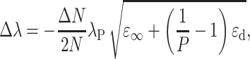 |
(1) |
where  is the permittivity of the surrounding dielectric medium,
  is the background high-frequency permittivity, P is the shape-dependent depolarization factor,
  is the plasmon wavelength, N is the carrier density and
  is the change in carrier density. The carrier density of Au cannot be easily modified by laser irradiation (446 nm) due to its high work function (5.0 eV). However, with the coating of semiconductor material such as the Cu2–xS, hot electron transfer from Au to Cu2–xS is possible. This is verified by transient absorption (TA) spectra, where the Au@Cu2–xS NPs show two typical modes at 573 and 890 nm, corresponding to the plasmon resonances of Au and Cu2–xS, respectively (Fig. 3d and e). The TA of Au@Cu2–xS NPs (at 573 nm) presents a lifetime of 0.38 ps, which is approximately six times faster than that of Au NPs (Fig. 3f upper panel and Supplementary Figure S5a and c), suggesting that CT happens from Au to the Cu2–xS shells. As the Cu2–xS shells receive electrons from Au, their TA spectra decay (at 890 nm) also appears slightly slower than that of the Cu2–xS NPs (Fig. 3f lower panel and Supplementary Figure S5b and d). As such, the electron density of Au is reduced due to such CT (Fig. 3g), which results in a positive value of Δλ as predicted by using Equation (1). Thus, red shift of LSPR is observed when the excitation laser is on, which can shift back due to electron backflow when the laser is switched off (Fig. 2c). With 641-nm laser irradiation, however, no obvious electron dynamics was observed for pure Au NPs (Supplementary Figure S6a) but a clear CT process still happens in the hybrid Au@Cu2–xS NPs (Supplementary Figure S6b), indicating that 641-nm light mainly excites the Cu2–xS, whose electrons transfer to the Au NP (Supplementary Figs S3c and S6c and d). As such, the electron density of Au NP increases, which results in a slight blue shift (Supplementary Figure S3a) as predicted by using Equation (1).
When Au@Cu2–xS NPs are placed on metal films, NPoM constructs are established and a circuit model is applied to qualitatively analyse the antenna mode of this plasmonic system as [16]:
 |
(2) |
where  and
and  are the capacitance of the structure and NP, respectively. Here we approximate
  using the formula
 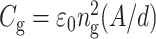 , where A and d are the area of the bottom facet of the Au NP and the gap size, respectively [37]. Since the capacitance is mainly determined by the size of the gap/NP and their dielectric properties, modifying either of these parameters will shift the plasmon resonances (
 ). In a certain NPoM structure in which the gap size and dielectric environment are fixed, the gap conductance is critical to the shift in plasmon resonances. The conductance increase contributed from the photothermal effect is small (0.2G0, Supplementary Figure S7) [38]. Thus, the major contribution to the conductance increase is the hot electron transfer from Au to Cu2–xS, which then transports to the Au substrate (Fig. 3h). The conductivity of Cu2–xS in the nanogap can be calculated as
 , where n and
  are the charge density and carrier mobility within Cu2–xS. e is the unit charge. For 80 nm of Au NPoM with a facet diameter of 10 nm and gap of 5 nm, the calculated gap conductance increase due to hot electron tunneling is ∼32G0 (see Methods for the detailed calculation). This large conductance increase can lead to a 18-nm blue shift as predicted by using numerical analysis (Fig. 3i and Supplementary Figure S8), which agrees with the blue shift observed in the experiments (Fig. 2h). Again, with 641-nm laser excitation, because the CT process happens from Cu2–xS to Au NPs or Au films (Supplementary Figure S3d), a negligible change in gap conductance is expected, which reasonably explains no shift in the coupled plasmons (Supplementary Figure S3b).
As the plasmon resonance is determined by the gap conductance, increasing the irradiation power would lead to an increase in the hot carrier concentration (n), which would increase the gap conductance (G). Therefore, we see an increasing blue shift of the gap plasmons with the increase in irradiation power (Fig. 4a and b). The magnitude of the blue shift can also be attenuated with shell thickness. Here, we synthesized Au@Cu2–xS NPs of different shell thicknesses by adding different amounts of precursors, which yields uniform shells ranging from 5 to 25 nm (Supplementary Figure S9). As the shell thickness increases, the magnitude of the blue shift increases proportionally at the same pumping power (Fig. 4c–f), which is likely due to the increased carrier mobility of thicker shells [39].
Figure 4.

Power- and thickness-dependent plasmon shift of Au@Cu2–xS NPoMs. (a) Scattering spectra of Au@Cu2–xS NPoM at different irradiation power. (b) Change in plasmon resonance with irradiation power. (c)–(e) Scattering spectra of Au@Cu2–xS NPoMs of different shell thickness: (c) 5 nm, (d) 15 nm, (e) 25 nm. Pumping power: 5 mW. (f) Change in blue-shift magnitude with shell thickness. All the error bars are the averaged and squared deviation based on five NPoMs.
CONCLUSION
In summary, we have demonstrated a dynamic and reversible tuning strategy of plasmon resonances based on optical modulation of hot carrier transport in the semiconductor coating. The hot electrons are generated from interband excitation (446 nm) of Au NP and transfer to the Cu2–xS coating, which reduces the electron density of Au, thereby red-shifting the LSPR. In the NPoM geometry, such CT enhances the conductance of the plasmonic nanogaps, which results in blue shift of the coupled plasmon resonances. Excitation with a longer-wavelength laser (641 nm) mainly results in excitation of Cu2–xS, which induces CT from Cu2–xS to Au. As such, we see a slight blue shift of the plasmons due to the increase in the electron density. But this CT does not strongly affect the coupled plasmons in the NPoM geometry as it does not significantly alter the gap conductance. A finite element method (FEM) is applied to simulate the conductance-induced plasmon shift, which agrees well with the experimental results. Unlike the conventional plasmon-tuning strategy, this intriguing tuning mechanism is based on optoelectronic excitation of hot carriers as well as the modification of electron density and gap conductance, which is fast (∼THz) and chip-compatible, meeting the high demands of the ultracompact on-chip integration of functional nanophotonic circuits and photonic computation.
METHODS
Synthesis of Au@Cu2–xS core–shell NPs
The Au@Cu2–xS core–shell NPs were synthesized according to a previous report [26]. Specifically, 50 μL of 0.2 M cetyltrimethylammonium bromide (CTAB), 50 μL of 0.1 M hexamethylenetetramine (HMT), 50 μL of 0.1 M AA, 50 μL of 0.01 M TAA and 0.01 M cupric chloride (CuCl2) with varied volume were sequentially added into vials containing 1 mL of Au NP dispersion (Nanopartz), which were incubated at 85°C for 8 h. The hybrid core–shell NPs were harvested by centrifugation at 8000 r/min for 10 min and redispersed in 1 mL of deionized water for stock use.
Characterizations
UV–vis extinction spectra of the Au NPs and hybrid Au@Cu2–xS core–shell NPs were collected using an optofiber spectrometer (QE65000, Ocean Optics). The Raman spectra of Cu2–xS were obtained using a confocal Raman microscope (Renishaw InVia) equipped with a 532-nm laser. TEM images and energy dispersive EDS were captured at an accelerating voltage of 200 kV (JEOL JEM-F200). Scanning electron microscope (SEM) images were obtained using a Sigma Zeiss at an accelerating voltage of 10 kV. XPS (Thermo Fisher ESCALAB 250Xi) were performed using a monochromatic Al K Alpha (1 486.68 eV) X-ray source under an ultra-high vacuum (10−7 mbar). The X-ray high-tension (HT) was 15 kV and the measured spot size was 200 μm.
Optical switching of the plasmon resonances based on Au@Cu2–xS NPoM system
To construct the NPoM system, Au@Cu2–xS NPs were drop-casted on Au films, which were then placed under a dark-field (DF) microscope (BX53M, Olympus). The scattering spectra of the NPs were recorded confocally through a 100 × DF objective (numerical aperture (NA): 0.8) that were coupled using a 50-μm optical fiber connected to a spectrometer (integration time: 800 ms, QEPro, Ocean Optics). DF scattering spectra were collected simultaneously when an excitation laser (CW) of 446 nm was on. The power of the CW laser was 5 mW and the duration of the laser on/off periods was 1 s each. The PL spectra of the same Au@Cu2–xS NPoMs were recorded, which were then used to subtract the scattering spectra to exclude the influence of PL on the shift of plasmons (Supplementary Figure S2). The scattering spectra of Au@Cu2–xS NP on SiO2 substrate were measured in the same way as a contrast experiment.
Ultrafast TA spectroscopy
The TA spectra of the Au NPs, Cu2–xS NPs and Au@Cu2–xS NPs were collected using a commercial TA system (HARPIA, Light Conversion). Specifically, a femtosecond laser (repetition rate of 40 kHz, 1030-nm central wavelength and pulse duration of ∼120 fs, PHAROS, Light Conversion) was split into two beams. One beam went through optical parametric amplification (ORPHEUS twins, Light Conversion) to pump the Au@Cu2–xS NPs. The other beam went through the delay line, which yields the white light via sapphire as the probe beam. The pump and probe beams were focused on Au@Cu2–xS dispersion in a cuvette with wavelengths of 400 and 640 nm. Single exponential fitting  was applied to the TA spectra, which resolves the lifetime of τ.
Simulations
The near-field scattering and temperature profile of Au@Cu2–xS NPs on Au film and SiO2 substrate are numerically simulated using FEM. Specifically, a plain wave incidence with energy density equivalent to a Gaussian beam was applied at the Au@Cu2–xS NPoMs. The thermal conductivity of Au, Cu2–xS and SiO2 are 318, 1.5 and 1.8 W (m·K)−1, respectively. The RI of Cu2–xS is set at an average value of 1.8 with an imaginary part of 0.02 [40,41]. Gap conductance is calculated based on the formula  , where l is the gap size (∼5 nm) and S is the area of the bottom facet of the Au NP with a radius of ∼5 nm. Conductivity of the gap was calculated based on the formula
  , where n is the carrier density change induced by the hot electron injection, which is ∼1026 m−3;
  is the carrier mobility of Cu2S, which is estimated to be 0.01 m2·(V·s)−1 [39]; and e is the unit charge (1.6 × 10⁻¹⁹).
Supplementary Material
ACKNOWLEDGEMENTS
The numerical calculations in this paper have been performed using the supercomputing system in the Supercomputing Centre of Wuhan University. We thank the Centre for Nanoscience and Nanotechnology and Electron Microscope Centre at Wuhan University for SEM, TEM and XPS characterizations. Dr. Yong Liu is acknowledged for his assistance with XPS analysis.
Contributor Information
Jiacheng Yao, Key Laboratory of Artificial Micro/Nano Structure of Ministry of Education, School of Physics and Technology, Wuhan University, Wuhan 430072, China.
Cheng Wang, Key Laboratory of Artificial Micro/Nano Structure of Ministry of Education, School of Physics and Technology, Wuhan University, Wuhan 430072, China.
Chi Zhang, Key Laboratory of Artificial Micro/Nano Structure of Ministry of Education, School of Physics and Technology, Wuhan University, Wuhan 430072, China.
Song Ma, Key Laboratory of Artificial Micro/Nano Structure of Ministry of Education, School of Physics and Technology, Wuhan University, Wuhan 430072, China.
Li Zhou, Key Laboratory of Artificial Micro/Nano Structure of Ministry of Education, School of Physics and Technology, Wuhan University, Wuhan 430072, China.
Ti Wang, Key Laboratory of Artificial Micro/Nano Structure of Ministry of Education, School of Physics and Technology, Wuhan University, Wuhan 430072, China.
Ququan Wang, Department of Physics, Southern University of Science and Technology, Shenzhen 518055, China.
Hongxing Xu, Key Laboratory of Artificial Micro/Nano Structure of Ministry of Education, School of Physics and Technology, Wuhan University, Wuhan 430072, China.
Tao Ding, Key Laboratory of Artificial Micro/Nano Structure of Ministry of Education, School of Physics and Technology, Wuhan University, Wuhan 430072, China.
FUNDING
This work was supported by the National Key Research and Development Program of China (2020YFA0211300), the National Natural Science Foundation of China (12374356, 11974265, 12074296 and 12174294) and the Fundamental Research Funds for the Central Universities (2042023kf0211).
AUTHOR CONTRIBUTIONS
T. D. conceived the idea and supervised the project. J. Y., C. Z. and S. M. synthesized the samples, J. Y. performed all the characterizations. C. W., J. Y. and C. Z. performed TA measurements and data analysis. T. D. and J. Y. performed analytic and numerical calculations. J. Y., T. D., T. W., L. Z., Q. W. and H. X. discussed and analysed the data, wrote and revised the manuscript. All the authors approve the final version of the manuscript.
Conflict of interest statement. None declared.
REFERENCES
- 1. Brongersma ML, Shalaev VM. The case for plasmonics. Science 2010; 328: 440–1. 10.1126/science.1186905 [DOI] [PubMed] [Google Scholar]
- 2. Jiang N, Zhuo X, Wang J. Active plasmonics: principles, structures, and applications. Chem Rev 2018; 118: 3054–99. 10.1021/acs.chemrev.7b00252 [DOI] [PubMed] [Google Scholar]
- 3. Wurtz GA, Pollard R, Hendren W et al. Designed ultrafast optical nonlinearity in a plasmonic nanorod metamaterial enhanced by nonlocality. Nat Nanotechnol 2011; 6: 107–11. 10.1038/nnano.2010.278 [DOI] [PubMed] [Google Scholar]
- 4. Wang X, Morea R, Gonzalo J et al. Coupling localized plasmonic and photonic modes tailors and boosts ultrafast light modulation by gold nanoparticles. Nano Lett 2015; 15: 2633–9. 10.1021/acs.nanolett.5b00226 [DOI] [PubMed] [Google Scholar]
- 5. Rotenberg N, Caspers JN, van Driel HM. Tunable ultrafast control of plasmonic coupling to gold films. Phys Rev B 2009; 80: 245420. 10.1103/PhysRevB.80.245420 [DOI] [Google Scholar]
- 6. Chen F, Wang Y, Wang S et al. Plasmon-assisted nanopoling of poly(vinyl difluoride) films. Adv Opt Mater 2021; 9: 2100084. 10.1002/adom.202100084 [DOI] [Google Scholar]
- 7. Cormier S, Ding T, Turek V et al. Actuating single nano-oscillators with light. Adv Opt Mater 2018; 6: 1701281. 10.1002/adom.201701281 [DOI] [Google Scholar]
- 8. Li Q, Chen L, Xu H et al. Photothermal modulation of propagating surface plasmons on silver nanowires. ACS Photonics 2019; 6: 2133–40. 10.1021/acsphotonics.9b00711 [DOI] [Google Scholar]
- 9. Kaya S, Weeber JC, Zacharatos F et al. Photo-thermal modulation of surface plasmon polariton propagation at telecommunication wavelengths. Opt Express 2013; 21: 22269–84. 10.1364/OE.21.022269 [DOI] [PubMed] [Google Scholar]
- 10. Wang Y, Ding T. Optical tuning of plasmon-enhanced photoluminescence. Nanoscale 2019; 11: 10589–94. 10.1039/C9NR03725J [DOI] [PubMed] [Google Scholar]
- 11. Xing J, Zhao C, Zou Y et al. Modulating the optical and electrical properties of MAPbBr3 single crystals via voltage regulation engineering and application in memristors. Light Sci Appl 2020; 9: 111. 10.1038/s41377-020-00349-w [DOI] [PMC free article] [PubMed] [Google Scholar]
- 12. Michel A-KU, Chigrin DN, Maß TWW et al. Using low-loss phase-change materials for mid-infrared antenna resonance tuning. Nano Lett 2013; 13: 3470–5. 10.1021/nl4006194 [DOI] [PubMed] [Google Scholar]
- 13. Rudé M, Simpson RE, Quidant R et al. Active control of surface plasmon waveguides with a phase change material. ACS Photonics 2015; 2: 669–74. 10.1021/acsphotonics.5b00050 [DOI] [Google Scholar]
- 14. Seo M, Kyoung J, Park H et al. Active Terahertz nanoantennas based on VO2 phase transition. Nano Lett 2010; 10: 2064–8. 10.1021/nl1002153 [DOI] [PubMed] [Google Scholar]
- 15. Zhang C, Li D, Zhang G et al. Switching plasmonic nanogaps between classical and quantum regimes with supramolecular interactions. Sci Adv 2022; 8: eabj9752. 10.1126/sciadv.abj9752 [DOI] [PMC free article] [PubMed] [Google Scholar]
- 16. Benz F, de Nijs B, Tserkezis C et al. Generalized circuit model for coupled plasmonic systems. Opt Express 2015; 23: 33255–69. 10.1364/OE.23.033255 [DOI] [PubMed] [Google Scholar]
- 17. King PDC, Veal TD. Conductivity in transparent oxide semiconductors. J Phys: Condens Matt 2011; 23: 334214. [DOI] [PubMed] [Google Scholar]
- 18. Qazilbash MM, Brehm M, Chae BG et al. Mott transition in VO2 revealed by infrared spectroscopy and nano-imaging. Science 2007; 318: 1750–3. 10.1126/science.1150124 [DOI] [PubMed] [Google Scholar]
- 19. Rini M, Cavalleri A, Schoenlein RW et al. Photoinduced phase transition in VO2 nanocrystals: ultrafast control of surface-plasmon resonance. Opt Lett 2005; 30: 558–60. 10.1364/OL.30.000558 [DOI] [PubMed] [Google Scholar]
- 20. Lei DY, Appavoo K, Sonnefraud Y et al. Single-particle plasmon resonance spectroscopy of phase transition in vanadium dioxide. Opt Lett 2010; 35: 3988–90. 10.1364/OL.35.003988 [DOI] [PubMed] [Google Scholar]
- 21. Orlianges JC, Leroy J, Crunteanu A et al. Electrical and optical properties of vanadium dioxide containing gold nanoparticles deposited by pulsed laser deposition. Appl Phys Lett 2012; 101: 133102. 10.1063/1.4754708 [DOI] [Google Scholar]
- 22. Boyce AM, Stewart JW, Avila J et al. Actively tunable metasurfaces via plasmonic nanogap cavities with Sub-10-nm VO2 films. Nano Lett 2022; 22: 3525–31. 10.1021/acs.nanolett.1c04175 [DOI] [PMC free article] [PubMed] [Google Scholar]
- 23. Ma S, Yang DJ, Ding SJ et al. Tunable size dependence of quantum plasmon of charged gold nanoparticles. Phys Rev Lett 2021; 126: 173902. 10.1103/PhysRevLett.126.173902 [DOI] [PubMed] [Google Scholar]
- 24. Majeski MW, Bolotin IL, Hanley L. Cluster beam deposition of Cu2–xS nanoparticles into organic thin films. ACS Appl Mater Interfaces 2014; 6: 12901–8. 10.1021/am5028428 [DOI] [PubMed] [Google Scholar]
- 25. Gómez-Solano RE, Arias-Cerón JS, Ríos-Ramírez JJ et al. Synthesis and study of structure and phase composition in Cu2–xS, SnxSy, ZnS, CuxSnSy and CuZnSnS pellets. J Mater Sci: Mater El 2020; 31: 7519–23. [Google Scholar]
- 26. Ma S, Chen K, Qiu YH et al. Controlled growth of CdS–Cu2−xS lateral heteroshells on Au nanoparticles with improved photocatalytic activity and photothermal efficiency. J Mater Chem A 2019; 7: 3408–14. 10.1039/C8TA11154E [DOI] [Google Scholar]
- 27. Wang S, Ding T. Photothermal-assisted optical stretching of gold nanoparticles. ACS Nano 2019; 13: 32–7. 10.1021/acsnano.8b06087 [DOI] [PubMed] [Google Scholar]
- 28. Li G-C, Zhang Y-L, Jiang J et al. Metal-substrate-mediated plasmon hybridization in a nanoparticle dimer for photoluminescence line-width shrinking and intensity enhancement. ACS Nano 2017; 11: 3067–80. 10.1021/acsnano.7b00048 [DOI] [PubMed] [Google Scholar]
- 29. Zhang Q, Liu D, Ren Q et al. Probing electron transport in plasmonic molecular junctions with two-photon luminescence spectroscopy. Nanophotonics 2021; 10: 2467–79. 10.1515/nanoph-2021-0116 [DOI] [Google Scholar]
- 30. Chen F, Liu Y, Ding T. Fast and hydrosensitive switching of plasmonic nanocavities via photothermal effect. Photon Res 2023; 11: 12–9. 10.1364/PRJ.470930 [DOI] [Google Scholar]
- 31. Chen F, Yao J, Wang X et al. Fast modulation of surface plasmons based on the photothermal effect of nonvolatile solid thin films. Nanoscale 2023; 15: 476–82. 10.1039/D2NR05527A [DOI] [PubMed] [Google Scholar]
- 32. Wang S, Guo L, Wen X et al. Phase transitions in the Cu2S nanowires. Mater Chem Phys 2002; 75: 32–8. 10.1016/S0254-0584(02)00026-3 [DOI] [Google Scholar]
- 33. Liang X, Jin D, Dai F. Phase transition engineering of Cu2S to widen the temperature window of improved thermoelectric performance. Adv Electron Mater 2019; 5: 1900486. 10.1002/aelm.201900486 [DOI] [Google Scholar]
- 34. Ho KHW, Shang A, Shi F et al. Plasmonic Au/TiO2-dumbbell-on-film nanocavities for high-efficiency hot-carrier generation and extraction. Adv Funct Materi 2018; 28: 1800383. 10.1002/adfm.201800383 [DOI] [Google Scholar]
- 35. Peng Z, Lo TW, Lei D. Plasmonic-hot-electron mediated room-temperature generation of charged biexciton in monolayer WS2. Phys Rev Materi 2023; 7: 054002. 10.1103/PhysRevMaterials.7.054002 [DOI] [Google Scholar]
- 36. Mulvaney P, Pérez-Juste J, Giersig M et al. Drastic surface plasmon mode shifts in gold nanorods due to electron charging. Plasmonics 2006; 1: 61–6. 10.1007/s11468-005-9005-0 [DOI] [Google Scholar]
- 37. Benz F, Tserkezis C, Herrmann LO et al. Nanooptics of molecular-shunted plasmonic nanojunctions. Nano Lett 2015; 15: 669–74. 10.1021/nl5041786 [DOI] [PMC free article] [PubMed] [Google Scholar]
- 38. Bekenstein Y, Elimelech O, Vinokurov K et al. Charge transport in Cu2S nanocrystals arrays: effects of crystallite size and ligand length. Z Phys Chem 2015; 229: 179–90. 10.1515/zpch-2014-0593 [DOI] [Google Scholar]
- 39. Ubale AU, Choudhari DM, Kantale JS et al. Synthesis of nanostructured CuxS thin films by chemical route at room temperature and investigation of their size dependent physical properties. J Alloys Compd 2011; 509: 9249–54. 10.1016/j.jallcom.2011.07.009 [DOI] [Google Scholar]
- 40. Zhang J, Xing T, Zhang M et al. Facile preparation of Cu2-xS supernanoparticles with an unambiguous SERS enhancement mechanism. Chem Eng J 2022; 434: 134457. 10.1016/j.cej.2021.134457 [DOI] [Google Scholar]
- 41. Saadeldin M, Soliman HS, Ali HAM et al. Optical and electrical characterizations of nanoparticle Cu2S thin films. Chin Phys B 2014; 23: 046803. 10.1088/1674-1056/23/4/046803 [DOI] [Google Scholar]
Associated Data
This section collects any data citations, data availability statements, or supplementary materials included in this article.