Abstract
Using a stainless shadow mask combined with a magnetron-ion-assisted deposition (IAD) sputtering system, we investigate the surface morphologies and optical properties of microfilms. Optimal color-filter (CF) coating microfilms with niobium pent-oxide (Nb2O5)/silicon dioxide (SiO2) multilayers on a hard polycarbonate (HPC) substrate, grown at 85 °C and 50 SCCM oxygen flow, can obtain a fairly uniform thickness (with an average roughness of 0.083 and 0.106 nm respectively for Nb2O5 and SiO2 films) through all positions. On a flexible HPC substrate with the Nb2O5/SiO2 microfilms, meanwhile, the peak transmittances measured in the visible range are 95.70% and 91.47%, respectively, for coatings with and without a shadow mask for this new-tech system. For the optimal CF application with a shadow mask, transmittance on each 100 nm band-pass wavelength is enhanced by 4.04% absolute (blue), 2.96% absolute (green), and 2.12% absolute (red). Moreover, the developed new-tech system not only enhances the quality of the films by achieving smoother and uniform surfaces but also reduces deposition time, thereby improving overall process efficiency. For the with-shadow-mask condition, there is little shift at 50% transmittance (T50%), and high transmittance (~97%) is maintained after high-temperature (200 °C) baking for 12 h. These results are well above the commercial CF standard (larger than 90%) and demonstrate reliability and good durability for flexible optical applications.
Keywords: shadow mask, ion-assisted deposition (IAD), color filter (CF), uniform thickness, flexible substrate, 50% transmittance (T50%)
1. Introduction
In the realm of sputtering technologies for depositing microfilms, achieving uniformity in the surface morphologies is paramount for ensuring optimal performance across various applications [1,2,3,4,5]. Two problems generally occur in terms of the uniform distribution of the thickness deposited by the direct current (dc) reactive magnetron sputtering system. The first problem consists of an electrically insulating layer generated on the target surface during the high-temperature sputtering process, resulting in arcing due to charge accumulation. In particular, insulating film deposition on the electrode strongly affects the gas discharge properties, not only by blocking the current flow but also by discharging the dielectric surface fully by reverse pulses [6]. Furthermore, a high-temperature process with low discharging limits flexible application on hard polycarbonate (HPC) or stainless-steel substrates.
In the second non-uniform problem from magnetron sputtering, the distance between the target and substrate is often very short, and as a result, the coating thickness at different positions of the substrate depends on the sputtering distribution of the target material [7,8]. Without controlling the uniformity, a coating on a flat substrate is usually thick at the center, and the thickness gradually decreases toward the edges [8,9]. This limits the size and number of coating elements for multi-film applications that can be produced in a single coating run. In the case of curved optics, the desired thickness distribution cannot be achieved without effectively controlling the thickness. Thus, controlling the lateral thickness distribution is essential for coatings prepared by magnetron sputtering.
To solve these problems, ion-assistance deposition (IAD) equipped with a shadow mask with an adjustable stripe and length can be attached to a reactive magnetic sputter [10,11,12,13], allowing deposition for optical applications with smooth-surface and high-density microfilms under low-temperature operation. By evaluating the different deposition thicknesses at individual positions on the film surface, the stripe length of the shadow mask is adjusted, thus improving the uniformity and smoothness of the film surface [14].
Our aims are to demonstrate the environmental durability of this new technique and to deposit a multilayer to verify the new-tech advantages in enhancing the performance of flexible color-filter (CF) applications. In this research, therefore, we not only investigate the technique of IAD combined with adjustable shadow masks to improve the surface uniformity of microfilms but also conduct durability evaluations on the developed flexible CFs. These harsh environmental conditions include immersion in boiling water and saltwater as well as exposure to high temperature to enhance the CF performance and surface-morphology improvement from new-tech application opportunities.
2. Experiments and Measurements
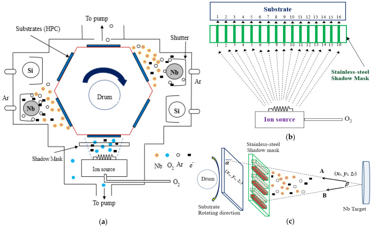
The block diagram of a reactive magnetron sputter equipped with an IAD system (as shown in Figure 1a) and the detailed thin stripe-length stainless-steel shadow mask (with 200 μm thickness, placed as shown in Figure 1b,c) to produce beneficial modifications in the surface morphologies for optical applications are provided [15]. In the developed IAD sputter in Figure 1a, there were niobium (Nb) and silicon (Si) targets, both with cylinder shapes, where cooling water flowed at the center during the sputtering process. A drum (at 60 rpm speed) under the 100 V pulse-dc voltage of discharging ions rotated each HPC substrate (with 30 × 30 mm2 dimension). The reactive sputtering also involved allowing sufficient reactive gases (Ar and O2) into the chamber to keep the target completely covered with a dielectric [16], for uniform film deposition of the Nb and Si materials with sequential and continuous coating.
Figure 1.
(a) Schematic diagram of the developed reactive magnetron sputter equipped with the IAD system and a shadow mask. (b) The detailed adjustable 16 positions of thin stripe-length stainless-steel shadow mask. A numerical optimal algorithm with trial–error iteration [17] optimizes the design of shadow-mask size (with 30 × 30 mm2 dimension and 200 μm thickness). (c) The orientation of the shadow mask relative to the targets. This takes into account the substrates on the rotating drum, sputtering targets, and a shadow mask with predefined stripe-length shape.
This study uses a vacuum coating system equipped with an electron beam gun. At the ambient temperature of the substrate, niobium pent-oxide (Nb2O5) and silicon dioxide (SiO2) thin films are deposited on the substrate through an electron beam supported by oxygen ions (O−). Meanwhile, as shown in Figure 1b, we added the detailed stripe-length shadow mask at 16 positions for measurement, hoping to enhance the uniformity of the new-tech color-filtering microfilms. Furthermore, Figure 1c illustrates the sputtering geometry in which the substrate is mounted on a rotating drum; β is the emission angle of the ejected particle flux relative to the normal to the target surface, and α is the incidence angle of the deposited particle flux relative to the normal to the substrate surface. On path A, the particles reach the substrate, and on path B, the shadow mask blocks the particles. In order to optimize the mask to achieve high uniformity over a large area, the sputtering yield, the angular distribution of the ejected particles from the target (path A), the mask restriction function, the arriving angle (α) of the sputtered particles on the substrate, and the substrate movement need to be taken into account.
Therefore, the chamber was first pumped down to 1 × 10⁻⁵ Torr or less. Then, the working Ar (99.99%) gas was applied with a flow rate of 55 and 85 SCCM (1 SCCM is identical to 1 atm cm3/min at STP), respectively, for Nb and Si targets. Pure O2 gas (99.99%) with a 50 SCCM flow rate, 125 W sputtering power, and 85 °C deposition temperature could also be introduced into the vacuum system to assist oxidation during the deposition process (deposition rate was 2.04 and 3.43 nm/min, respectively, for Nb2O5 and SiO2 microfilms). The total working pressure was ~5.1 × 10⁻⁴ Torr, with mean 0.2 A sputtering current. The s-polarized component of the light transmitted by the coated substrate was monitored at 550 nm during deposition of the layers and at 5 nm intervals over the 400~700 nm spectral range after deposition.
To measure the optical properties of the developed CFs, we used a spectrophotometer (Hitachi UV-Visible-NIR, Tokyo, Japan) to measure the transmittance within the visible wavelength range (400–700 nm). Additionally, we employed a scanning electron microscope (SEM, Hitachi S-4100) and atomic force microscopic (AFM, Digital Instruments Inc. (Tonawanda, NY, USA), NanoScope E with dimension 3100 controller) system to observe the surface morphology in this experiment. The surface roughness (RMS for Rq) values were obtained with the software that came with the instrument.
3. Results and Discussion
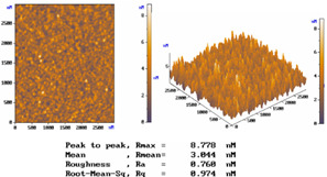
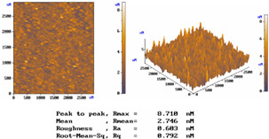
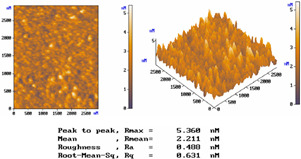
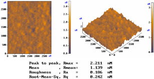
Table 1 lists the morphology comparison of Nb2O5 (at top, ~400 nm thickness) and SiO2 (at bottom, ~600 nm thickness) microfilms as deposited with (at right)/without (at left) shadow-mask conditions. The corresponding surface morphology (2D and 3D AFM images below), in which Rmax, Ra, and Rq stand for the maximum surface height, average centerline, and root-mean-square (RMS) roughness, respectively.
Table 1.
The comparisons of Nb2O5 and SiO2 microfilms and the corresponding surface morphology (AFM images below) deposited with/without mask condition. Layer thicknesses of Nb2O5 and SiO2 microfilms are about 600 and 400 nm, respectively.
| Nb2O5 Film (~400 nm thickness) | |||||
| Conditions | Rmax | Rmean | Ra | Rq (RMS) | |
| Without Mask | 8.778 nm | 3.044 nm | 0.760 nm | 0.974 nm | |
| With Mask | 8.710 nm | 2.746 nm | 0.603 nm | 0.792 nm | |
| SiO2 Film (~600 nm thickness) | |||||
| Conditions | Rmax | Rmean | Ra | Rq (RMS) | |
| Without Mask | 5.36 nm | 2.211 nm | 0.488 nm | 0.631 nm | |
| With Mask | 2.211 nm | 1.139 nm | 0.186 nm | 0.242 nm | |
| Nb2O5 Film (Without Mask) | Nb2O5 Film (With Mask) | ||||
|
|
||||
| SiO2 Film (Without Mask) | SiO2 Film (With Mask) | ||||
|
|
||||
For the without-shadow-mask condition, Nb2O5 or SiO2 film images show a relatively compact and flat surface structure; the film was composed of cone-shaped columns randomly distributed over the surface of the film. Thus, the films’ surface was rough and non-uniform, with the maximum surface height (Rmax)/average centerline (Ra)/RMS (Rq) surface roughness of 8.778/0.760/0.974 nm and 5.360/0.488/0.631 nm, respectively, for Nb2O5 and SiO2 microfilms. For the with-shadow-mask condition, the Rmax/Ra/Rq values are 8.710/0.603/0.792 nm and 2.211/0.186/0.242 nm, respectively, for Nb2O5 and SiO2 microfilms, being much smoother and uniformly distributed over the film surface. Meanwhile, this shadow-mask design could adjust the stripe length in accordance with different positions, thus shortening the morphology roughness and improving surface uniformity. Shadow-mask sizes are typically adjusted for uniform optimization via the preferential sputtering caused by ion bombardment [16].
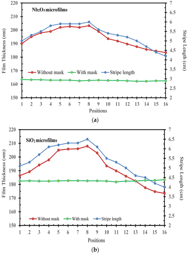
Figure 2 illustrates a comparison of the deposition thicknesses at various positions for Nb2O5 and SiO2 microfilms prepared with/without a shadow mask in the developed magnetron-IAD sputtering system. For comparison with/without a shadow mask, Nb2O5 microfilm-roughness ranges are large, from 19.86 to only 1.33 nm. Similarly, SiO2 microfilm-roughness ranges are large, from 34.5 to only 1.7 nm. For the condition with a stripe-length shadow mask, significantly, all the films’ surface morphologies were smooth and uniform, with less roughness, with a decrease in morphology roughness similar to the phenomena in the AFM images (values of Rmax, Ra, and Rq) of Table 1.
Figure 2.
The adjustable stripe length of the shadow mask with the magnetron-IAD sputtering system and the corresponding film thicknesses as a function at the 16 positions for the (a) Nb2O5 and (b) SiO2 microfilm deposition.
The roughness of SiO2 films is significantly less than that of Nb2O5 films. The surface morphology becomes rougher as the layer thickness increases, both with/without shadow mask conditions, as shown in the bottom-left axis of Figure 2. In Figure 2b, meanwhile, the SiO2 film thickness with the mask is higher in positions 13–16 than without the mask, which is consistent with the stripe-length trend (blue lines). This phenomenon may be attributed to the deposited material accumulating on the evolving edges of the micro-crystallites [18]. It can also illustrate that the adjustment trend of the stripe length is related to the thickness of the deposited film. Without masking, locations corresponding to thicker film deposition have shorter stripe length, while locations corresponding to thinner film deposition have longer stripe length.
For the without-shadow-mask condition (red lines in the bottom-left axis of Figure 2), it can be found that the thickness of the microfilm first increases corresponding to the position number from 1 to 8 and then decreases from the 9th to the 16th position. The microfilms’ surfaces were rough and non-uniform, with an average roughness of 1.241 and 2.156 nm, respectively, for Nb2O5 and SiO2 films. It can be inferred that the adjustment trend of the stripe length of the mask is related to the thickness of the microfilm deposition [9,14]. On the bottom-relation axes of Figure 2, therefore, the stripe length (blue line referred as the right-Y axis) at all positions should be adjusted by following this trend (red line referred as the left-Y axis). For the with-shadow-mask condition (green lines in the bottom-left axis of Figure 2), consequently, it can be verified by the above trend that a fairly uniform thickness is obtained (with an average roughness of 0.083 and 0.106 nm, respectively, for Nb2O5 and SiO2 films) through all corresponding positions.
The major CF design is a combination of high and low refractive indices, i.e., Nb2O5/SiO2 microfilms, of multilayer coatings [19]. The refractive indices (n) and extinction coefficient (k) can be calculated by Equations (1) and (2) [20,21]:
| (1) |
and
| (2) |
where
where ns is the substrate refractive index; TM and Tm are the maximum and minimum transmittance of the spectrum, respectively; d is the film thickness; λ1 and λ2 are the adjacent maximum and minimum wavelength, respectively; and n1 and n2 are the refractive indices corresponding to λ1 and λ2.
In the manufacturing of color-filtering applications, the layering process causes particles to settle between and on top of each layer. Consequently, all layers, including the CF coatings, have rough surfaces, posing challenges for accurately determining the (n, k, d) parameters through inverse methods due to scattering effects [19]. To obtain the (n, k, d) effective values simultaneously [19], mean square errors (MSEs) between measured and fitted reflectivity for a wide range of illuminations are minimized.
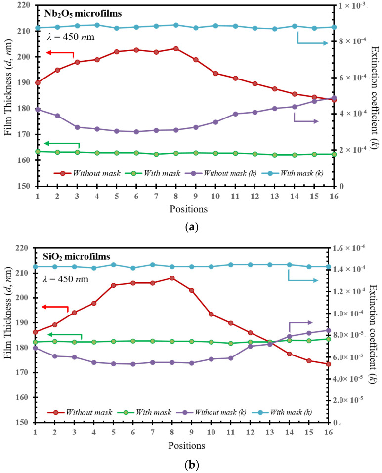
For the (n, k, d) effective values calculated by Equations (1) and (2), the optimal Nb2O5/SiO2-bilayer thickness can be determined for the layer numbers required to enhance the CF performance. Thus, Figure 3 and Figure 4 demonstrate the (n, k, d) relationship under the discharge current range (3–8 A) of the ion source and at λ = 450 nm with/without shadow masks, respectively, from the (k, d) and (n, d) parameter models. In the (k, d) model depicted in Figure 3, the roughness of the film thickness (d, in nm at the bottom-left axis) and the extinction coefficient (k, in ×10−5 order at the bottom-right axis) as a function at the various 16 positions, respectively, are given for (a) Nb2O5 and (b) SiO2 microfilms as compared with/without shadow masks. For the comparison with/without a shadow mask, the k values (blue lines) were increased by 0.019% (from 3.01 to 4.90 × 10⁻⁴ for Nb2O5 film) and 3.0 × 10⁻³% (from 1.42 to 1.45 × 10⁻⁴ for SiO2 film), respectively. In contrast, the d values (green lines) were, respectively, decreased by 18.53 nm (from 19.86 to only 1.33 nm for Nb2O5 film) and 32.8 nm (from 34.5 to only 1.7 nm for SiO2 film) as compared with/without a shadow mask in the developed IAD-sputter system. Therefore, the curve rate of change (in %) of k and d values is 0.7% or 0.8%, respectively, becoming smoother, with a uniform surface. Meanwhile, in Figure 3a,b, it can be seen that the k values of Nb2O5 films are higher than those for the films of SiO2. This is because SiO2 usually shows lower absorption characteristics in the visible spectrum range (400–700 nm wavelength), while Nb2O5 films can show higher absorption; the same argument can be found in [22].
Figure 3.
The comparison of the extinction coefficient (k) and the corresponding film thicknesses as a function at 16 different positions for (a) Nb2O5 and (b) SiO2 microfilms with/without shadow masks, respectively measured for the (k, d) parameter model.
Figure 4.
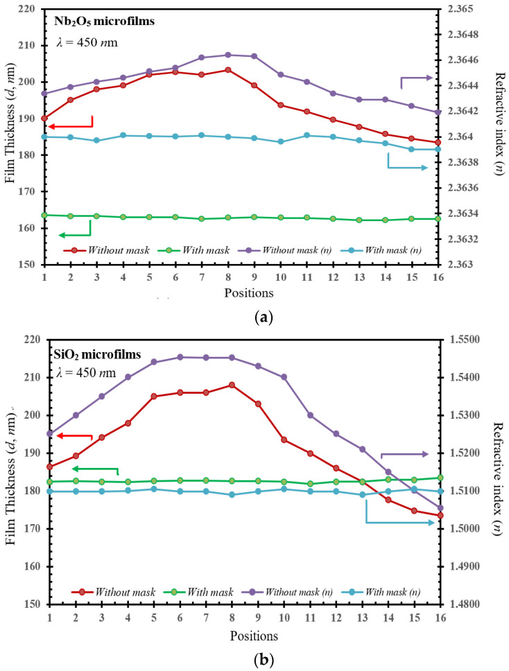
The comparison of the refractive index (n) and the corresponding film thicknesses as a function at 16 different positions for the (a) Nb2O5 and (b) SiO2 microfilm with and without shadow masks, respectively measured for the (n, d) parameter model.
Similarly, for the (n, d) parameters plotted in Figure 4, the difference of the film thickness (d, in nm at the bottom-left axis) and the refractive indices (n, at the bottom-right axis) as a function at the various 16 positions, respectively, are given for (a) Nb2O5 and (b) SiO2 microfilms as compared with/without shadow masks. It can be seen that the curve tendency of the n and d values becomes smoother, with a uniform surface, after using the shadow mask in the developed magnetron-IAD sputtering system. For the comparison with/without a shadow mask, the n values (blue lines) were increased by 0.045% (from 2.36419 to 2.36464 for Nb2O5 film) and 3.98% (from 1.5055 to 1.5453 for SiO2 film), respectively.
It can be observed that the n value of the film without the shadow mask increases as the d values increase, showing a proportional relationship consistent with the literature [23]. In contrast, since the d values (green lines) of the films produced with mask remain uniform, the change in n values is quite small, with only 0.011% variation (from 2.36390 to 2.36410 for Nb2O5 film) and 3.98% variation (from 1.5055 to 1.5453 for Si2O2 film), respectively, as compared with/without a shadow mask in the developed IAD-sputter system.
Meanwhile, in Figure 4a,b, it can also be seen that the n values of Nb2O5 films are higher than those for the films of SiO2. This is because SiO2 is a non-metal oxide with a simpler structure, and its refractive index is usually lower. In contrast, Nb2O5 is a metal oxide with a complex structure composed of niobium and oxygen atoms, and its refractive index may be higher. This is the same argument as found in [24].
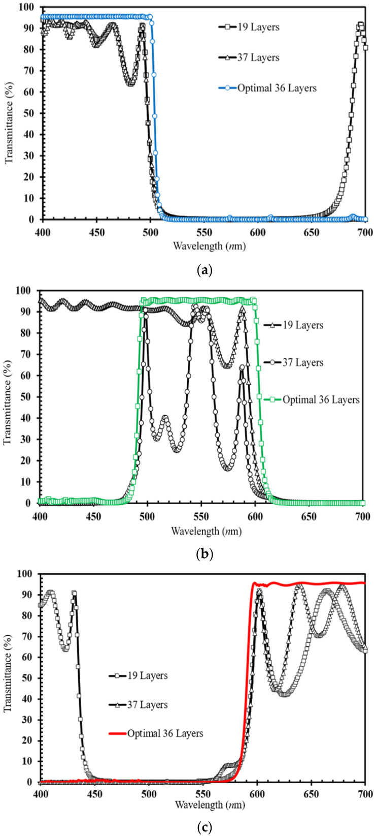
Following this (n, k, d) effective model, we can evaluate the optimal Nb2O5/SiO2-bilayer thickness and determine the layer numbers required to enhance the CF performance. Thus, Figure 5a–c depict the layer-number evaluation (19~37 layers) required for the narrow band-pass wavelength, respectively, for the blue (B), green (G), and red (R) regions. At the same time, in Figure 5, the optimal number of 36 layers can be determined from the narrow bandwidth (100 nm wavelength) for (a) B region (400–500 nm wavelength), (b) G region (500–600 nm wavelength) and (c) R region (600–700 nm wavelength).
Figure 5.
Transmittance comparisons between the experimental data and the calculated values from fitted (n, k, d) for CFs, respectively, at the (a) blue (400–500 nm wavelength), (b) green (500–600 nm wavelength), and (c) red (600–700 nm wavelength) narrow band-pass regions.
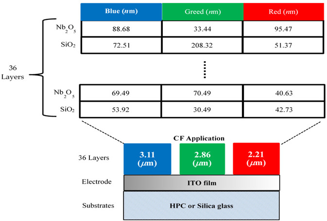
The values of the optimal 36-multilayer (Nb2O5/SiO2-bilayer) thicknesses of the RGB CF coatings determined from the effective (n, k, d) model of Figure 5a–c are listed in Table 2a. The total 36-multilayer thicknesses are 2.27, 2.86, and 3.11 μm for the RGB CF coatings. Table 2b plots the optimal 36-layer CFs using a flexible HPC substrate (30 × 30 mm2 dimension) and the developed magnetron-IAD with a shadow-mask sputtering system.
Table 2.
The design parameters of CF application. (a) Each value of the optimal 36-layer thickness for the RGB-filter design, and (b) the schematic structure coating on a flexible HPC substrate (with 2.27–3.11 μm 36-layer thickness and 30 × 30 mm2 dimensions) by the developed IAD-sputtering shadow-mask system.
| Layer No. | Materials | Blue (nm) | Materials | Green (nm) | Materials | Red (nm) |
|---|---|---|---|---|---|---|
| 1 | Nb2O5 | 88.68 | Nb2O5 | 33.44 | Nb2O5 | 51.37 |
| 2 | SiO2 | 72.51 | SiO2 | 208.32 | SiO2 | 95.47 |
| 3 | Nb2O5 | 77.72 | Nb2O5 | 53.21 | Nb2O5 | 46.69 |
| 4 | SiO2 | 104.64 | SiO2 | 88.38 | SiO2 | 60.74 |
| 5 | Nb2O5 | 50.16 | Nb2O5 | 50.8 | Nb2O5 | 58.74 |
| 6 | SiO2 | 114.59 | SiO2 | 31.57 | SiO2 | 86.72 |
| 7 | Nb2O5 | 63.81 | Nb2O5 | 39.72 | Nb2O5 | 53.51 |
| 8 | SiO2 | 90.03 | SiO2 | 87.3 | SiO2 | 89.31 |
| 9 | Nb2O5 | 58.52 | Nb2O5 | 52.12 | Nb2O5 | 51.35 |
| 10 | SiO2 | 118.93 | SiO2 | 87.14 | SiO2 | 76.69 |
| 11 | Nb2O5 | 50.42 | Nb2O5 | 48.13 | Nb2O5 | 85.81 |
| 12 | SiO2 | 94.5 | SiO2 | 29.07 | SiO2 | 55.64 |
| 13 | Nb2O5 | 68.67 | Nb2O5 | 44.68 | Nb2O5 | 55.37 |
| 14 | SiO2 | 95.41 | SiO2 | 88.81 | SiO2 | 89.31 |
| 15 | Nb2O5 | 59.86 | Nb2O5 | 55.83 | Nb2O5 | 47.77 |
| 16 | SiO2 | 94.52 | SiO2 | 70.86 | SiO2 | 85.07 |
| 17 | Nb2O5 | 68.84 | Nb2O5 | 117.67 | Nb2O5 | 117.88 |
| 18 | SiO2 | 91.41 | SiO2 | 99.89 | SiO2 | 45.9 |
| 19 | Nb2O5 | 61.59 | Nb2O5 | 72.11 | Nb2O5 | 47.98 |
| 20 | SiO2 | 109.15 | SiO2 | 97.2 | SiO2 | 64.15 |
| 21 | Nb2O5 | 76.77 | Nb2O5 | 99.87 | Nb2O5 | 52.39 |
| 22 | SiO2 | 167.97 | SiO2 | 109.35 | SiO2 | 79.56 |
| 23 | Nb2O5 | 75.99 | Nb2O5 | 60.94 | Nb2O5 | 20.62 |
| 24 | SiO2 | 109.41 | SiO2 | 129.06 | SiO2 | 71.25 |
| 25 | Nb2O5 | 64.96 | Nb2O5 | 75.56 | Nb2O5 | 47.44 |
| 26 | SiO2 | 101.2 | SiO2 | 141.68 | SiO2 | 42.11 |
| 27 | Nb2O5 | 86.55 | Nb2O5 | 63.64 | Nb2O5 | 46.29 |
| 28 | SiO2 | 166.54 | SiO2 | 98.73 | SiO2 | 66.22 |
| 29 | Nb2O5 | 68.15 | Nb2O5 | 89.84 | Nb2O5 | 54.71 |
| 30 | SiO2 | 115.67 | SiO2 | 130.8 | SiO2 | 78.49 |
| 31 | Nb2O5 | 64.19 | Nb2O5 | 70.27 | Nb2O5 | 63.17 |
| 32 | SiO2 | 88.72 | SiO2 | 105.79 | SiO2 | 76.52 |
| 33 | Nb2O5 | 76.02 | Nb2O5 | 98.46 | Nb2O5 | 51.69 |
| 34 | SiO2 | 91.92 | SiO2 | 32.49 | SiO2 | 67.28 |
| 35 | Nb2O5 | 69.49 | Nb2O5 | 70.49 | Nb2O5 | 42.73 |
| 36 | SiO2 | 53.92 | SiO2 | 30.19 | SiO2 | 40.63 |
| Total (μm) | 3.11 | 2.86 | 2.21 | |||
| ||||||
| (a) | ||||||
| ||||||
| (b) | ||||||
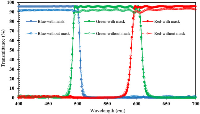
To verify the shadow-mask effect on the surface uniformity of microfilms, we compare the 36-layer transmittance for all RGB CFs sputtered by the developed system. For each color filter using the shadow mask, Table 3 shows that there was a great enhancement in the transmittance on each 100 nm band-pass wavelength by 4.04%absolute (blue CF with 3.11 μm thickness), 2.96%absolute (green CF with 2.86 μm thickness), and 2.12% absolute (red CF with 2.21 μm thickness). This shadow-mask CF design can also improve the narrow-band transmitting property, which corresponds to enhancing the surface uniformity, as presented in the AFM images of Table 1. Thus, it is the surface-roughness effect of the CF microfilm at a given wavelength, the same argument as found in [25], that is related to its high transmittance.
Table 3.
The RGB-CF transmittance comparison and the corresponding wavelength plot (below), with/without shadow-mask, by the magnetron-IAD sputter.
| Filters | Blue Filter (400~500 nm) |
Green Filter (500~600 nm) | Red Filter (600~700 nm) | |
|---|---|---|---|---|
| Condition | ||||
| Thickness | 3.11 μm | 2.86 μm | 2.21 μm | |
| With Mask | 95.5041% | 95.6174% | 95.7046% | |
| Without Mask | 91.4657% | 92.6601% | 93.5871% | |
In the process of CF development, conducting stability verification before mass production is crucial. This phase ensures that the product can withstand various harsh conditions and meets the expected performance standards. Evaluation and testing in hot water, saltwater, and high temperatures were conducted on the flexible CFs with a Nb2O5/SiO2 multilayer coating.
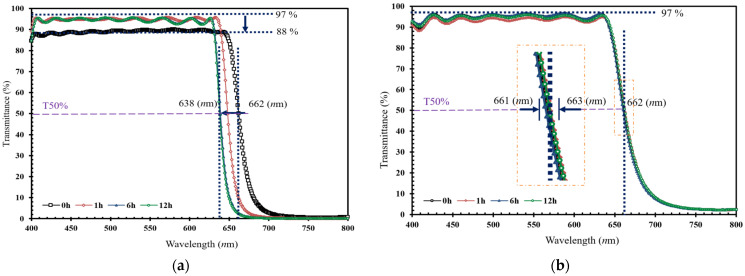
Figure 6 illustrates the changes in light transmittance of the CFs after high temperature (200 °C) from 0 to 12 h. In Figure 6a, it can be observed that, in the meantime, the T50% (at 50% transmittance) relative transmittance wavelength of the filters prepared as unmasked shifts from 662 to 638 nm wavelength (decreasing by 3.63%), and the transmittance decreases from 97% to 88% (variation of 9%absolute). In comparison, the CF in Figure 6b maintains the transmittance and wavelength at 662 nm (T50% variation for 0.3%absolute) and 97%, respectively.
Figure 6.
The comparison of the transmittance changes (in the visible range) of CFs fabricated by the magnetron-IAD sputtering system (a) without and (b) with a shadow mask, for environmental durability at 200 °C for 0, 1, 6, and 12 h. The cut-off wavelengths are quoted (with long-dash line) at the 50% (T = 50%) relative transmission.
After immersion in boiling (100 °C) water for 4 h and salt (100%) water for 3 days, the developed CFs with the shadow mask showed variations at T50% of 4.39 and 2.16%absolute, respectively, which can be considered negligible (both less than 5%). Therefore, all the phenomena demonstrate that CFs deposited with the shadow mask are more stable under harsh environments for optical applications. This also demonstrates that this new-tech system can enhance CF durability and reliability.
4. Conclusions
In summary, the adjustable stripe lengths of the shadow mask with the magnetron-IAD sputtering system can enhance the surface thickness uniformity of Nb2O5/SiO2 microfilms. The important novelty of this study is that we constructed a (n, k, d) effective model and calculated the simulated reflectance spectra by incorporating the variable refractive index and thickness of each layer of Nb2O5/SiO2 microfilms. Following the (n, k, d) parameter model, the optimal Nb2O5/SiO2-bilayer thickness can be evaluated, and layer numbers required to enhance the CF performance can be determined.
The optimal 36-layer CF was fabricated and observed by AFM and SEM to determine surface morphology. Next, the transmittance was measured by a spectrophotometer. Thus, for each CF with the shadow mask, each 100 nm band-pass wavelength exhibited a great enhancement in the transmittance, by 4.04%absolute (blue CF), 2.96%absolute (green CF), and 2.12% absolute (red CF). Finally, the developed new-tech system was shown to improve both the performance and surface morphology of the flexible-CF application, thus ensuring great durability under harsh environmental conditions (such as hot-temperature baking, saltwater immersion, and boiling water treatment). All these results are well above the commercial CF standard (larger than 90%), showing the reliability and durability of this developed new-tech system.
Author Contributions
All authors conceived the idea. D.-L.L., J.H., C.-C.Y. and S.-S.W. worked on the experiments and analyzed the data. T.-C.L. wrote the paper. J.-J.H. edited and revised the paper. All authors participated in the discussion of the results and proofread the paper. D.-L.L. and J.-J.H. supervised the project. All authors have read and agreed to the published version of the manuscript.
Data Availability Statement
The data presented in this study are available on request from the corresponding author. The data are not publicly available due to privacy and ethical restrictions.
Conflicts of Interest
The authors declare no conflict of interest. The funder was not involved in the study design, collection, analysis, interpretation of data, the writing of this article or the decision to submit it for publication.
Funding Statement
The authors acknowledge financial support from The National Science and Technology Council of R.O.C. under contract No. NSTC 112-2634-F-019-001 and Litefilm Technology Co., Ltd., Taiwan.
Footnotes
Disclaimer/Publisher’s Note: The statements, opinions and data contained in all publications are solely those of the individual author(s) and contributor(s) and not of MDPI and/or the editor(s). MDPI and/or the editor(s) disclaim responsibility for any injury to people or property resulting from any ideas, methods, instructions or products referred to in the content.
References
- 1.Vergöhl M., Werner O., Bruns S. New developments in magnetron sputter processes for precision optics. SPIE. 2008;7101:1–17. doi: 10.1117/12.797190. [DOI] [Google Scholar]
- 2.Halenkovič T., Kotrla M., Gutwirth J., Nazabal V., Nĕmec P. Insight into the photo-induced phenomena in ternary Ge-Sb-Se sputtered thin films. Photonics Res. 2022;10:2261–2266. doi: 10.1364/PRJ.460552. [DOI] [Google Scholar]
- 3.Yu X., Wang C., Liu Y., Yu D., Xing T. Recent Development in Magnetron Sputtering. Plasma Sci. Technol. 2006;8:337–343. doi: 10.1088/1009-0630/8/3/20. [DOI] [Google Scholar]
- 4.Chen K.-N., Hsu C.-M., Liu J., Liou Y.-C., Yang C.-F. Investigation of Antireflection Nb2O5 Thin Films by the Sputtering Method under Different Deposition Parameters. Micromachines. 2016;7:151. doi: 10.3390/mi7090151. [DOI] [PMC free article] [PubMed] [Google Scholar]
- 5.Welzel T. Ph.D. Thesis. TU-Chemnitz; Chemnitz, Germany: 2010. [(accessed on 9 March 2024)]. Time-Resolved Characterisation of Pulsed Magnetron Discharges for the Deposition of Thin Films with Plasma Diagnostic Methods. Available online: https://www.researchgate.net/publication/44449638. [Google Scholar]
- 6.Belkind A., Freilich A., Scholl R. Using pulsed direct current power for reactive sputtering of Al2O3. J. Vac. Sci. Technol. A. 1999;17:1934–1940. doi: 10.1116/1.581706. [DOI] [Google Scholar]
- 7.Sidelev D.V., Krivobokov V.P. Angular thickness distribution and target utilization for hot Ni target magnetron sputtering. Vacuum. 2019;160:418–420. doi: 10.1016/j.vacuum.2018.12.001. [DOI] [Google Scholar]
- 8.Broadway D.M., Platonov Y.Y., Gomez L.A. Achieving desired thickness gradients on flat and curved substrates. SPIE. 1999;1788:262–274. doi: 10.1117/12.363643. [DOI] [Google Scholar]
- 9.Wang B., Fu X., Song S., Chu H.O., Gibson D., Li C., Shi Y., Wu Z. Simulation and Optimization of Film Thickness Uniformity in Physical Vapor Deposition. Coatings. 2018;8:325. doi: 10.3390/coatings8090325. [DOI] [Google Scholar]
- 10.Fernandez D.A.R., Brito B.S.S., Santos I.A.D., Soares V.F.D., Terto A.R., de Oliveira G.B., Hubler R., Batista W.W., Tentardini E.K. Effect of hafnium contaminant present in zirconium targets on sputter deposited ZrN thin films. Nucl. Inst. Methods Phys. Res. B. 2020;462:90–94. doi: 10.1016/j.nimb.2019.11.005. [DOI] [Google Scholar]
- 11.Zhou G., Tian Y., Shi F., Song C., Tie G., Zhou G., Xie L., Shao J., Wu Z. Low-Energy Pulsed Ion Beam Technology with Ultra-High Material Removal Resolution and Widely Adjustable Removal Efficiency. Micromachines. 2021;12:1370. doi: 10.3390/mi12111370. [DOI] [PMC free article] [PubMed] [Google Scholar]
- 12.Ho J.-J., Chen C.-Y., Huang C.-M., Lee W.-J., Liou W.-R., Chang C.C. Ion-Assisted Sputtering Deposition of Antireflection. [(accessed on 3 March 2022)];Appl. Opt. 2005 44:6176–6180. doi: 10.1364/AO.44.006176. Available online: https://pubmed.ncbi.nlm.nih.gov/16237931/ [DOI] [PubMed] [Google Scholar]
- 13.Chen S., Sun J., Li J., Yi K., Wang C., Shao J., Zhu M. Controlling lateral thickness distributions of magnetron sputtering deposited coatings using shadow masks. Opt. Mater. 2024;14:101–114. doi: 10.1364/OME.500104. [DOI] [Google Scholar]
- 14.Oshima Y., Kawara K., Shinohe T., Hitora T., Kasu M., Fujita S. Epitaxial lateral overgrowth of α-Ga2O3 by halide vapor phase Epitaxy. APL Mater. 2019;7:022503. doi: 10.1063/1.5051058. [DOI] [Google Scholar]
- 15.Li C., Song S., Gibson D., Child D., Chu H.O., Waddell E. Modeling and validation of uniform large-area optical coating deposition on a rotating drum using microwave plasma reactive sputtering. Appl. Opt. 2017;56:C65–C70. doi: 10.1364/AO.56.000C65. [DOI] [PubMed] [Google Scholar]
- 16.Khazaal H.F., Hburi I.S., Farhan M.S. The Impact of ion-beam parameters on the characteristics of Nb2O5 thin films. Surf. Interfaces. 2020;20:100593. doi: 10.1016/j.surfin.2020.100593. [DOI] [Google Scholar]
- 17.Guo C., Kong M., Liu C., Li B. Optimization of thickness uniformity of optical coatings on a conical substrate in a planetary rotation system. Appl. Opt. 2013;52:B26–B32. doi: 10.1364/AO.52.000B26. [DOI] [PubMed] [Google Scholar]
- 18.Elsholz F., Schöll E., Scharfenorth C., Seewald G., Eichler H.J., Rosenfeld A. Roughness evolution in thin-film growth of SiO2 and Nb2O5. J. Appl. Phys. 2005;98:2130521. doi: 10.1063/1.2130521. [DOI] [Google Scholar]
- 19.Lee Y.-M., Cheng H.-H., Li J.-H., Kuen T.-Y., Sheng Y.-T. Refractive Index and Effective Thickness Measurement System for the RGB Color Filter Coatings with Absorption and Scattering Properties. J. Disp. Technol. 2014;10:57–70. doi: 10.1109/JDT.2013.2285577. [DOI] [Google Scholar]
- 20.Manifacier J.C., Gasiot J., Fillard J.P. A simple method for the determination of the optical constants n, k and the thickness of a weakly absorbing thin film. J. Phys. E Sci. Instrum. 1976;9:1002–1004. doi: 10.1088/0022-3735/9/11/032. [DOI] [Google Scholar]
- 21.Caglar M., Caglar Y., Ilican S. The Determination of the Thickness and Optical Constants of the ZnO Crystalline Thin Film by Using Envelope Method. [(accessed on 13 March 2024)];J. Optoelectron. Adv. Mater. 2006 8:1410–1413. Available online: https://www.researchgate.net/publication/228671678. [Google Scholar]
- 22.Yuan Z.-S., Jhang J.-M., Yu P.-H., Jiang C.-M., Huang Y.-C., Wu Y.-L., Lin J.-J., Yang C.-F. Comparisons of Theoretical and Experimental Results of Blue Light SiO2–Nb2O5 Distributed Bragg Reflector Fabricated Using E-beam deposition. Vacuum. 2020;182:109782. doi: 10.1016/j.vacuum.2020.109782. [DOI] [Google Scholar]
- 23.Lalova A., Todorov R. Optical properties of thin PMMA films for sensor application. [(accessed on 13 March 2024)];Bulg. Chem. Commun. 2015 47:29–34. Available online: http://bcc.bas.bg/BCC_Volumes/Volume_47_Special_B_2015/BCC-47-SI-B-5.pdf. [Google Scholar]
- 24.Kim S., In J.-H., Kim S.H., Han K., Lim D., Hwang Y.S., Lee K.M., Choi J.H. Study of High Transmittance of SiO2/Nb2O5 Multilayer Thin Films Deposited by Plasma-Assisted Reactive Magnetron Sputtering. Appl. Sci. 2023;13:13271. doi: 10.3390/app132413271. [DOI] [Google Scholar]
- 25.Zhang K., Forouhi A.R., Bloomer I. Accurate and rapid determination of thickness, n and k spectra, and resistivity of indium–tin–oxide films. J. Vac. Sci. Technol. A. 1999;17:1843–1847. doi: 10.1116/1.581902. [DOI] [Google Scholar]
Associated Data
This section collects any data citations, data availability statements, or supplementary materials included in this article.
Data Availability Statement
The data presented in this study are available on request from the corresponding author. The data are not publicly available due to privacy and ethical restrictions.


