Summary
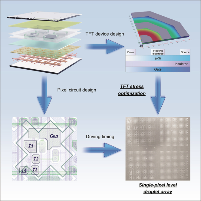
Digital liquid sample handling is an enabling tool for cutting-edge life-sciences research. We present here an active-matrix thin-film transistor (TFT) based digital microfluidics system, referred to as Field Programmable Droplet Array (FPDA). The system contains 256 × 256 pixels in an active area of 10.65 cm2, which can manipulate thousands of addressable liquid droplets simultaneously. By leveraging a novel TFT device and circuits design solution, we manage to programmatically manipulate droplets at single-pixel level. The minimum achievable droplet volume is around 0.5 nL, which is two orders of magnitude smaller than the smallest droplet ever reported on active-matrix digital microfluidics. The movement of droplets can be either pre-programmed or controlled in real-time. The FPDA system shows great potential of the ubiquitous thin-film electronics technology in digital liquid handling. These efforts will make it possible to create a true programmable lab-on-a-chip device to enable great advances in life science research.
Subject areas: Chemistry, Fluidics, Physics
Graphical abstract
Highlights
-
•
A fully new designed active-matrix digital microfluidics has been proposed
-
•
New TFT device and pixel circuit structure have been designed for the FPDA chip
-
•
The FPDA chip can generate thousands of individually addressable droplets easily
-
•
The minimum droplet of 0.5 nL is capable to be used in single-cell applications
Chemistry; Fluidics; Physics
Introduction
For decades, very large-scale integrated circuits (VLSI) has greatly changed people’s lives and paved the way to the digital era.1,2 There are two broad categories of VLSI: application-specific integrated circuits (ASICs) and field programmable gate arrays (FPGAs).3 ASICs are customized designs targeted to solve specific tasks, while FPGA can be reprogrammed to meet the desired application specifications or functionality requirements.4 Due to its programmability and flexibility, FPGAs tend to be preferred for rapid prototype verification of ASIC or high-speed communication interface.5
Recently, numerous lab-on-a-chip (LOC) platforms have emerged along with innovative technologies for various application areas.6,7,8 LOCs can also be divided into two broad categories. One is the traditional microfluidics chip based on custom micro-channel designs, that will be referred to as integrated fluidic circuits (IFC),9 another is the digital microfluidics (DMFs) based on electrowetting-on-dielectric (EWOD). IFC usually involve the use of lithography to create micro-channels and reservoirs on a substrate, which is then bonded to another substrate either thermally or chemically to create a watertight seal. Just like ASIC chips, IFC’s channels are fixed for specific application scenarios. IFC have been in continuous development for more than 20 years toward not only the LOC, but also the micro-total analysis system (μTAS).10 While there are several unavoidable problems restricting its practical application, for instance, most IFC require a micro-pump for driving the liquid, which greatly increases the size and complexity of the platform; the liquid in IFC is usually continuous, or, even if discrete droplets can be generated, the droplets are not individually addressable; the micro-channels or micro-structures in IFC have a low yield, hence increasing its fabrication cost and hindering the commercial mass production.11,12,13
It is therefore necessary to build a new type of LOC which is not subject to the limitations mentioned above. The one-dimensional restriction of micro-channel have to be settled to allow the free movement of droplets in a two-dimensional planar surface. To solve this, EWOD has been introduced to manipulate droplets electrically.14 EWOD is a physical phenomenon which allows for the manipulation of liquid droplets by applying an electric field to change the wettability of the surface.15 Therefore, by utilizing an electrodes array, water droplets can be manipulated freely on the electrode array surface.16 Most of the existing DMF chips are based on passive electrode arrays, in which each electrode connects to the peripheral electronics directly. Due to the space limitation of driving signals and layout wiring, the scalability issues greatly restrict the scale of the passive-matrix electrode array.
Active matrix (AM) technology provides a perfect solution for addressing this issue.17 In an AM array, pixel circuits contain electronic switches and capacitors to store a logic voltage. Each pixel can be addressed by row and column signal scanning, thus realizing independent pixel control and scalability of the AM array. The additional benefit of the AM technology is for an array sized N (row) × M (column) is addressable by only N + M control signals. All the addressable pixels can be programmed to provide sequenced patterns for liquid droplets on chip to realize an FPDA for lab-on-a-chip applications (Figure S1). The droplets traditional DMF chips can handle is commonly less than 100. While active-matrix DMF can manipulate thousands of droplets individually, Due to its massive droplet array programmable nature, much like the FPGA, we can name it Field Programmable micro-Droplet Array (FPDA) to distinguish with the traditional DMF chips.
Compared to the IFC, the FPDA has no prefabricated micro-channels or micro-structures and each droplet on the FPDA could be addressed and controlled independently, thus achieving more flexible and complex droplets operations.18 Additionally, the fabrication of FPDA is based on standard thin-film processes, which is more mature and precise resulting in larger mass market production scalability.19,20 This makes FPDA a more attractive solution in a wider range of applications whereas beyond the ability of conventional IFC.
In this paper, novel designs of TFT structure and pixel circuits are proposed to improve the performance of FPDA chip. These innovative contributions play a crucial role in advancing the field of DMFs, offering significant improvements over conventional approaches. These designs could enhance the driving force, then enabling precise and reliable droplets manipulation. These advancements not only realize the overall functionality of DMFs but also pave the way for a wider range of applications where precise droplet manipulation is essential.
Results and discussion
Structure of FPDA chip
There are basically two kinds of micro-switch to realize FPDA chips, one is TFT, the other is complementary metal oxide semiconductor (CMOS). The TFT-based FPDAs are generally fabricated on glass substrate, while the CMOS-based chips are fabricated on silicon wafer, thus their fabrication cost is not in the same order of magnitude. In addition, the TFT-based FPDA chip possesses the ability of large area fabrication process and high optical transparency, which cannot be achieved on a traditional silicon wafer.21,22,23 These benefits indicate that, the TFT device is more suitable to be utilized in FPDA.
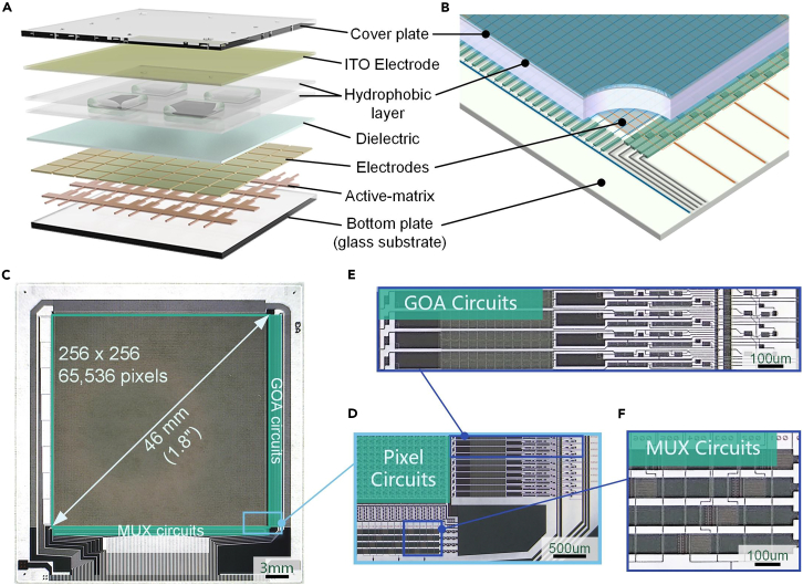
A full view of the FPDA chip is shown in Figure 1C, and the details of decomposed parts can be seen in Figures 1D–1F. The layout of FPDA chip can be seen in the Figure S2. As mentioned before, AM technology is an ideal method for solving the scalability issues present in PM matrix. Different functional circuits are designed to realize a massive scale active-matrix electrodes array by further reducing row and column driving signals. In AM matrix, each pixel can be individually addressed by the row and column scanning method, in which the row scan signals are transmitted line by line, so it is possible to use a shift register for generating and transmitting the row scan signals. The shift register circuits are also referred as to gate on array (GOA) and located on one side of the electrodes array (shown in Figure 1E). The GOA circuits can generate several hundreds of driving signals serially, while the GOA itself needs only 4 driving signals, thus it significantly reduces the number of external row driving signals. The outputs of column data is in parallel, and another circuit is designed to reduce the column driving signals instead of the serial GOA circuits. The circuit is simple and effective, and several TFTs control a column data signal into the pixel array. By turning each TFT device on in sequence, one data signal can be divided into several parallel driving signals. Here 4 TFTs is used to control one data signal, namely MUX circuits, so the number of column-driving signals has been reduced by 4 times. With these modifications, it is possible to address 65,536 pixels using less than 80 driving signals (Figure S3).
Figure 1.
Design of an active-matrix digital microfluidics based FPDA system
(A) Cross-section view; (B) 3D view; (C) photograph of a 256 × 256 pixels FPDA; (D) picture of a part of the array; (E) picture of the GOA circuits; (F) picture of the MUX circuits.
Thin-film transistor device structure optimization
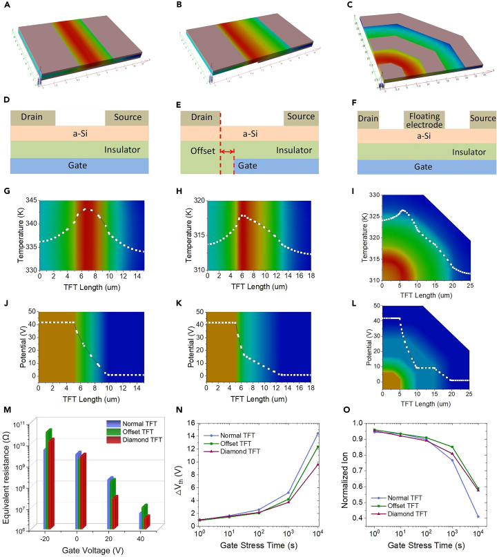
In order to realize large-area droplets manipulation, a well-designed driving strategy is necessary, which requires the design of TFT device and pixel circuit. The driving voltage requirement in FPDA is different from other applications, such as high voltage transmission and pixel voltage stability. We compared and simulated the TFT device and pixel circuit of the FPDA chip, and Figures 2G–2L shows the TCAD simulation results of channel temperature distribution and voltage drop across different TFT devices. Figures 2A and 2D is the structure of the normal bottom gate bottom contact (BGBC) TFT device, which is the common structure of amorphous silicon. The channel width/length (W/L) of the BGBC TFT is 20 μm/6 μm. When a high voltage up to 50 V is applied to the gate electrode and 40 V to the drain electrode, a drain current of around 100 μA is produced. High drain current stress causes the self-heating effect of the TFT device, which leads to performance degradation such as threshold voltage (Vth) shift, channel current drop, transconductance distortion, etc. Therefore, to improve the high-voltage performance of TFT device, the conventional method is to place a high-resistance area between the drain and channel, namely drain-offset.24 Figures 2B and 2E shows a typical structure of drain-offset TFT, where the gate electrode does not overlap with the drain electrode. The channel width of the offset TFT is 20 μm, with an offset length of 3 μm and a channel length of 6 μm. The drain-offset area could divide the high drain voltage applied to the channel, thus reducing the high drain current transferred in the channel. The disadvantage of a drain-offset TFT device is that the resistance of the offset area is very large, which increases the overall gate-on resistance and reduces the total channel on-current.
Figure 2.
Optimization of the TFT device in FPDA
(A–C) Stereogram of temperature distribution in normal TFT, offset TFT and diamond TFT; (D–F) cross section view of the three TFTs; (G–I) temperature curve with TFT length of the three TFTs; (J–L) potential variation with TFT position in the three TFTs; (M) equivalent resistance of different TFTs under different gate voltages; (N) threshold voltage stability of different TFTs under gate positive bias stress; (O) on current stability of the three TFTs under different gate positive bias stress time.
To address the above issues, a new structure of TFT was designed, as shown in Figures 2C and 2F, the structure of the new TFT looks like the side of a diamond, so we name it diamond TFT. The diamond TFT comprises two channels separated by a floating electrode. Both channels have a different width but are of equal length of 6 μm. The width of the inner most channel is 14 μm, whereas the width of outermost channel is 30 μm. Two channels in series can withstand the high voltages applied on the drain electrode, thus reducing the transverse electric field strength. Compared to the traditional single channel TFT, the floating electrode in diamond TFT could form a balanced electric field inside the channel, which improves the stability of the TFT device. Figures 2G–2I show the temperature-distribution simulation of the three TFT devices. Due to the different dimensions of the three devices, the device sizes were normalized. When the same voltage is applied to all three types of TFT devices, the channel temperature of conventional single channel device is the highest, and the channel temperature of diamond devices is between the offset device and single channel device. Figures 2J–2L show the potential distribution simulation of the three TFT devices. The channel of offset TFT serially connected to a high resistance region results in a significant voltage drop in that region. The diamond TFT also has a voltage drop in the inner channel, while the current transmission capability is better than the offset TFT device. To further compare the characteristics differences of the three TFT devices, the output curve of the TFT device was measured and the equivalent resistance was calculated. As shown in Figure 2M, when the gate is open, the channel resistance of diamond TFT is smaller than the offset TFT and the normal TFT, which means that the diamond TFT has a better current transmission characteristic. Additionally, the diamond TFT has better positive bias stress (PBS) stability, as shown in Figures 2N and 2O, after 10k seconds, the threshold voltage (Vth) shift of diamond TFT is less than 10V, while other TFTs are more than 10V (Figure S4).
Pixel circuit design and simulation
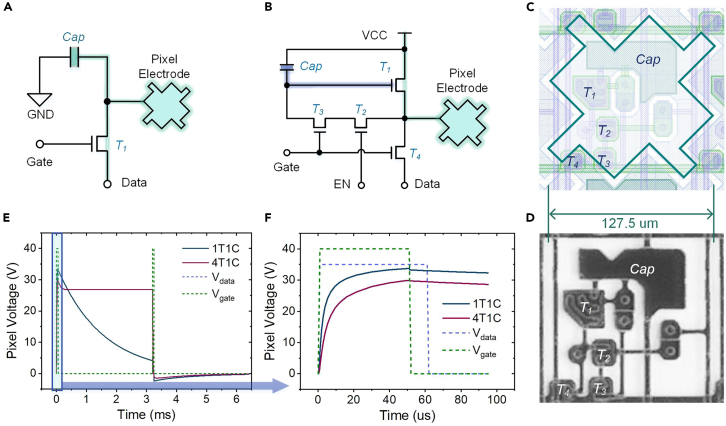
Based on the improved TFT device design, the FPDA chips were optimized for pixel circuit operation. Presently, there are mainly two types of pixel circuits reported: the 1T1C17 and the SRAM.25 Generally, the 1T1C circuit is a simple passive circuit (shown in Figure 3A), while the SRAM is a complicated active circuit. In the 1T1C circuit, the pixel electrode is driven by the charge stored in the capacitor. As capacitor is a passive component, the stored charge will gradually leak out from the TFT and pixel electrode. When under the circumstances of high temperature or light exposure, the leakage current will rise by several orders of magnitude. In this case, the leakage rate of the stored charge will be accelerated, which will greatly reduce the pixel voltage and the driving force of droplets. To avoid this, a power signal needs to be introduced into the pixel circuit to realize active driving.
Figure 3.
FPDA pixel circuit design
(A) a 1T1C pixel circuit; (B) a 4T1C pixel circuit; (C) the layout of the 4T1C pixel circuit, (D) a photomicrograph of the 4T1C circuit; (E) pixel electrodes voltage simulation of a 1T1C and a 4T1C circuit, (F) pixel electrodes voltage charge details of the 1T1C and the 4T1C circuit.
The SRAM is an ideal active circuit, the basic structure of which is bistable. The voltage of the pixel electrodes driven by the SRAM can remain constant, taking no account of the leakage current. Thus, the driving force on droplets can also be maintained continuously. So far there`s only one kind of SRAM circuit reported, which was designed by Sharp Life Science (EU) Ltd.26 The downside of the reported SRAM circuit is that the circuit requires about 14 TFTs. Increasing the number of TFT devices in a pixel circuit results in the pixel layout sized of 210 μm. It is difficult to reduce the layout space of the SRAM circuit any further. The more TFT devices in the pixel circuit, the larger the layout space occupied by the pixel, and the more limitation of its applications, such as single-cell sorting and large-area FPDA chips.
Considering the factors of driving ability and layout space, we designed a pixel circuit with only 4 TFTs and a capacitor (named 4T1C) based on the commercialized amorphous silicon (a-Si) process.27 As shown in Figure 3B, a power source VCC has been introduced into the pixel circuit to maintain the driving voltage. The pixel size is 127.5 μm (shown in Figures 3C and 3D), which is much smaller than the reported SRAM circuit sized 210 μm28 and the reported 1T1C circuit sized 1000 μm.17 Figures 3E and 3F simulated the pixel voltage of 1T1C circuit and 4T1C circuit. As the 4T1C circuit introduces a VCC power to drive the pixel electrode; the charge stored in the capacitor only needs to keep the gate voltage stable. Compared with the 1T1C circuit, the 3T1C design reduces the leakage path of capacitor stored charge. Thus, the gate voltage of driver TFT (T1) tends to remain stable, enhancing the driving ability of the pixel voltage.
When we fabricate the FPDA chip, except the design of TFT device and array circuits, there are also some items to be carefully considerate. Table 1 summarized the recommended specifications of different items of the FPDA chip, including the fabrication process parameters of the backplane glass substrate and the cover ITO glass. These parameters are obtained by continuous optimization and iteration of FPDA chip design, and have been verified the effectiveness by experiments. In this work, we have followed the recommended specifications to ensure the performance of FPDA chip.
Table 1.
Summary of the recommended specifications to fabricate the FPDA
| Components | Structure | Items | Recommended Specifications | This work |
|---|---|---|---|---|
| Substrate | TFT | Ion | ≥1E-6A | 1E-5A |
| Ioff | ≤1E-10A | 5E-11A | ||
| Vth | 0 ± 5V | 0∼4V | ||
| SS | ≤2V/dec | 1∼2V/dec | ||
| μ | ≥0.5cm2/(V·S) | 0.55cm2/(V·S) | ||
| Metal | Sheet resistance | ≤0.5Ω/□ | 0.4Ω/□ | |
| Dielectric | Εr | ≥5.5 | 6∼7 | |
| Breakdown strength | ≥2 MV/cm | 2∼3 MV/cm | ||
| Surface | Equal height area ratio | ≥60% | 60% | |
| Surface height difference | ≤5% gap | 5% | ||
| Outline | X/Y tolerance | ±0.15mm | ±0.12mm | |
| Z tolerance | ±0.05mm | ±0.04mm | ||
| Cover plate | Hydrophobic Layer | Contact angle | ≥110° | 120° |
| Rolling angle | ≤20° | 15° | ||
| ITO | Surface height difference | ≤50nm | 30∼40nm | |
| Sheet resistance | ≤100Ω/□ | 80Ω/□ | ||
| Transmittance | ≥85% | 90% | ||
| Inlet/outlet hole | Diam tolerance | ±5%diam | ±3% | |
| Location tolerance | ±50um | ±50um | ||
| Outline | X/Y tolerance | ±0.15mm | ±0.15mm | |
| Z tolerance | ±0.05mm | ±0.04mm |
Field Programmable Droplet Array for concentration gradients generation
Traditional IFC microfluidics are generally based on physical micro-channels. Comparatively, FPDA chips have no prefabricated micro-channels, thus the liquid manipulation process is quite different. On the traditional IFC microfluidics platform, the droplets are generated by the coordination of pumps and micro-channels. The flow path and volume of droplets on IFC microfluidics is commonly fixed and restricted, and it`s difficult to address and manipulate the target droplet. However, with FPDA chips, each individual droplet is addressable, and its volume can be controlled. The array scale of FPDA chips is much larger than that of the traditional IFC microfluidics. The massive pixels in the AM array pave the way for high-throughput and versatile reaction of liquid droplets, providing the ability to split, sort, and merge different sizes of droplets freely and dynamically. These liquid operations are routine on the FPDA chips, while being almost impossible using traditional microfluidic chips.
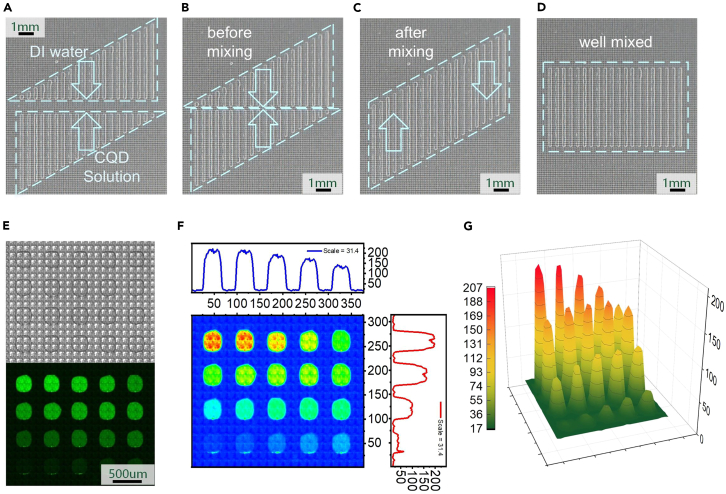
To further showcase the application scenarios of FPDA chips, an experiment was designed to realize different concentration gradients of Carbon quantum dots (CQDs) fluorescent solution. As shown in Figure 4A, liquid droplets were generated in various pixel size, which looks like they are being arranged by virtual channels. the droplets were then mixed by moving them back and forth to mix the reagent evenly (shown in Figures 4B–4D). Figures 4E and 4F show the bright field and fluorescence image of fluorescent solution with different concentration gradients. The fluorescence intensity value of different droplets has also been extracted in Figures 4G and 4H. It can be seen that, the 20 droplets have relatively different concentrations to each other, indicating that the AM-FPDA chip could realize a high-throughput concentration gradient by the virtual channel.
Figure 4.
Virtual channel microfluidics and droplets fluorescence intensity gradient
(A) virtual channel of DI water and CQDs fluorescent solution in different length; (B–D) Mixing of DI water and CQDs fluorescent solution; (E) Bright field and fluorescence images of fluorescent solution with different concentration gradients; (F) intensity value extracted from the fluorescence image; (G) Stereoscopic image of fluorescent solution with different concentration gradients.
Droplet array generation
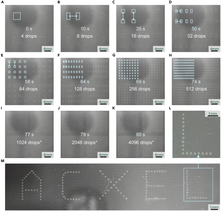
To realize the best control precision and highest array usage efficiency of FPDA chip, it`s necessary that a single pixel can drive a single droplet independently. The one-to-two droplets generation method has been applied to generate massive individual droplets in a short time. The bisection generation principle is simple and effective, one droplet subdivides into two, then two droplets divide into four, and so on. In this way, the number of single droplets can be increased exponentially (Figure S5). Figures 5A–5K shows the droplets generation process using the bisection method, and the time interval of each step is about 0.5s. Based on the bisection generation method, one droplet can be divided into two continuously. Under the control of AM electrode array, thousands of single droplets can be obtained in about 80s. As the pixel number of the FPDA chip is 65,536, it`s capable of generating an array with more than four thousand droplets (shown in Figure 5K). We know that droplets cannot be closely adjacent to each other, otherwise they will merge together, so the 8 pixels around a droplet cannot have any more droplets, thus the maximum number of droplets is 1/9th of all pixels in theoretical (65536). In practical operation, due to the droplet generation method is one-to-two, two-to-four, so the total number of droplets is a multiple of 2, that is 4096 on this FPDA chip. In order to illustrate the characteristic of programmable droplet array on FPDA, as shown in Figure 5M, we selected single-pixel droplets and arranged them into a word `ACXEL`. The detailed manipulation process is shown in Figure S6.
Figure 5.
High-throughput droplet array generation process and generation percentage
(A–K) the generation step time of different droplets size; (L) letter of ‘L’ formed by single-pixel droplets; (M) word of ‘ACXEL’ formed by single-pixel droplets.
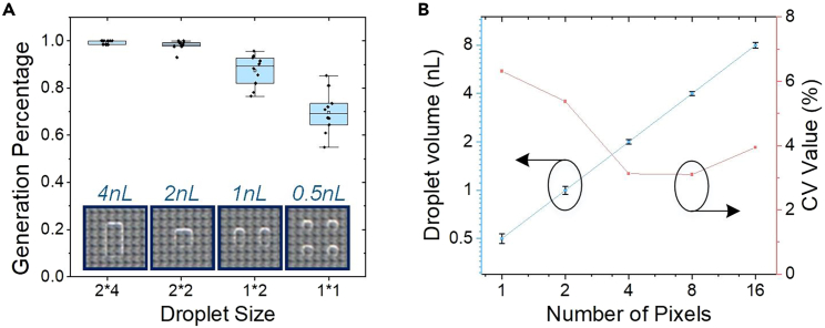
The droplet manipulation principle of FPDA chips is based on EWOD, which is sensitive to the driving signals and interface state. In the bisection process, the droplet volume keeps halving while the pixel pitch is constant. Therefore, the droplet would gradually approach the limit size that cannot be bisected. Figure 6A illustrates the generation percentage of droplets in different sizes. The size was defined by the number of pixels occupied by the droplet. When the droplet size was larger than 2x2, the success rate of droplets generation was close to 100%. When the droplet sized 2x2 divided into two droplets sized 1x2, the success rate would reduce to about 90%. The single-pixel droplet was the most difficult to be generated, whose typical success rate was about 70%. There is a limit in the minimum size of droplets generated by FPDA, which is related to the ratio of gap to droplet size. When the generation approaching the limit of droplet size, the coefficient of variation (CV) will also get worse. The CV is calculated by the measured droplets area (Table S1). As shown in Figure 6B, the CV of droplets lager than 2 nL is below 4, and would increase when generating smaller droplets. Especially when generating the single-pixel droplet, the droplet size is close to the limit to split, the force of EWOD is insufficient to break through the critical value of the surface tension, leading to the low success rate and poor CV.
Figure 6.
Characterization of the generated droplets
(A) generation success percentage of different droplets size; (B) droplet volume generated by different pixels and it`s coefficient of variation(CV).
The monodispersion and stability of droplets are crucial factors that determine the effectiveness and reliability of the FPDA chip. These factors can significantly impact the performance of various applications in FPDA, such as droplet generation, manipulation, and sample reactions. As the discussions above, the success rate of droplets generation differs with the droplet size, the smaller the droplet is, the lower the generation success rate. Fortunately, the most prominent feature of FPDA chip is programmable droplets, each of the droplet can be addressed and moved to the designated area. With the help of these advantages, massive droplets can be controlled precisely and achieving a high monodispersion and stability.
Limitations of the study
In this study, we have demonstrated a robust and powerful tool for generating and manipulating micro-droplets, namely the FPDA platform. Based the novel diamond TFT structure and 4T1C pixel circuits design, the FPDA chip could realize high throughput droplets generation and manipulation at the single-pixel level. There are 65,536 pixels in the FPDA chip, and all the droplets can be addressed and manipulated independently, with the minimum droplet volume of about 0.5 nL. The potential of the FPDA platform is to revolutionize applications in point-of-care diagnostics, drug development, and environmental monitoring. The high accuracy and real-time capabilities of FPDA chips offer greater sensitivity and specificity for detection and analysis of biomolecules and cells. Integration of multiple functionalities on a single chip could lead to new miniaturized analytical tools that are more accurate, efficient, and sensitive than current technologies. This work shows the great application potential of TFT technology in FPDA platform, to create new breakthroughs for the lab-on-a-chip systems. Based on the FPDA chip, the droplet analysis system could be further miniaturized along with a higher throughput and have the potential to be utilized in various bio-applications.
Methods
The carbon quantum dots solutions were purchased from Suzhou Xingshuo Nanotech Co., Ltd. (Suzhou, P.R.China), the concentration of 10 mg/mL, the extraction wavelength of 480 nm, the photoluminescent wavelength of 514 nm.
FPDA device fabrication
We designed and fabricated the FPDA device. The fabrication process of TFT-based FPDA is similar with the backplane of flat panel display, both of which are fabricated by thin film electronic technology and photolithography process. The structure of FPDA device is shown in Figures 1A and 1B, the amorphous silicon TFT array was fabricated on a glass substrate, an electrowetting dielectric layer (300 nm SiNx) and a hydrophobic layer was deposited on the top of the TFT array. A plastic spacer (not shown in Figure 1B) was used to define the gap (30 μm) between the bottom glass substrate and the ITO coated cover glass plate. The side of the ITO layer facing the bottom was also coated with a thin layer of hydrophobic material. The conductive ITO was constantly connected to the system ground, and a direct electric field was formed across the gap when a corresponding pixel located at the bottom is selected. The surrounding medium oil was used to suppress liquid droplet evaporation and enhance droplet mobility.
Electronics system
The FPDA device features an active-matrix array of 256 × 256 elements, totaling 65,536 addressable pixel electrodes. We use a MUX to separate 1 column signal into 4 columns. The MUX contains 4 TFTs controlling each TFT to open in sequence. The row signals are generated by the described GOA circuits. The GOA circuits require 4 driver signals, namely CK, CKB, STV and RST. The CK and CKB is two inversion clock signals; The STV is a stimulus signal to stimulate the GOA circuits; The RST is a reset signal to reset all the output signals of the GOA circuits. The FPDA needs 64 column signals and 4 GOA signals. We use a DC-DC power to supply the voltage for the FPDA platform, and a STM32 embedded system to control the driving signals. Researchers in the field can gain valuable insights into the potential of these novel designs, facilitating further advancements in the development of high-performance FPDA chips.
STAR★Methods
Key resources table
| REAGENT or RESOURCE | SOURCE | IDENTIFIER |
|---|---|---|
| Chemicals, peptides, and recombinant proteins | ||
| Hydrophobic materials | Chemours | Teflon AF1600 |
| UV-curing adhesives | ThreeBond | 3124P |
| Carbon Quantum Dots solutions | Xingshuo Nanotech | CQDs-515-Water |
| Other | ||
| DMatrix ecosystem | ACX inst | www.acxel.com |
| FPDA chip backplane | TIANMA MPG | www.tianma.cn |
| ITO cover glass | TOKEN | STN-5 |
Resource availability
Lead contact
Further information and requests for resources should be directed to and will be fulfilled by the lead contact, Hanbin Ma (mahb@sibet.ac.cn).
Materials availability
This study did not generate new unique reagents.
Data and code availability
-
•
The published article includes all datasets generated or analyzed during this study.
-
•
This paper does not report original code.
-
•
Any additional information required to reanalyze the data reported in this paper is available from the lead contact upon request.
Method details
FPDA chip packaging
-
1.
Ultrasonic clean the indium-tin-oxide(ITO) cover glass and FPDA chip substrate with acetone, IPA, and deionized water for 5 minutes respectively.
-
2.
Bake the ITO cover glass and FPDA chip substrate at 120°C on a hot platform for 5 minutes.
-
3.
Spin coating a hydrophobic layer on the ITO cover glass and FPDA chip substrate.
-
4.
Soft bake the hydrophobic layer at 40°C for 10 minutes.
-
5.
Hard bake the hydrophobic layer at 180°C for 20 minutes, to form a hydrophobic thin film of 50 nm.
-
6.
Mix resin beads with a particle size of 30um into UV curing adhesive, the weight ratio of resin beads and ultraviolet(UV) curing resin is 3:100.
-
7.
Apply the mixed UV curing resin around the FPDA chip substrate, apply the silver colloid onto the grounding electrode on the FPDA chip substrate.
-
8.
Align and fit the ITO cover glass and FPDA chip substrate, Illuminate with 365nm ultraviolet light for 30 seconds to solidify the UV curing resin.
-
9.
Bonding Flexible Printed Circuit board(FPC) connector onto the FPDA chip substrate, finish the FPDA Chip packaging process.
Droplet array generation
-
1.
Inject 100uL silicone oil onto the FPDA chip through the oil injection hole.
-
2.
Inject 2uL deionized(DI) water onto the FPDA chip through the liquid sample injection hole.
-
3.
Move DI water to the designated area of the FPDA chip.
-
4.
Control the computer software and start the automatic generation program of droplet array.
Concentration gradients generation
-
1.
Inject 100uL silicone oil onto the FPDA chip through the oil injection hole.
-
2.
Inject 1uL deionized(DI) water onto the FPDA chip through one of the liquid sample injection hole.
-
3.
Move DI water to the designated area of the FPDA chip.
-
4.
Seperate the DI water in different size, form the DI water into one column, resemble 20 virtual channels.
-
5.
Inject 1uL Carbon Quantum Dots(CQDs) solution onto the FPDA chip through another liquid sample injection hole.
-
6.
Move CQDs solution to the designated area of the FPDA chip.
-
7.
Seperate the CQDs solution in different size, form the CQDs solution into one column, resemble 20 virtual channels.
-
8.
Mix the DI water and CQDs solution one by one, resemble 20 virtual channels.
-
9.
Moving up and down mixed droplets to make the CQDs well-distributed in DI water.
-
10.
Split a 2 nL droplet from each of the mixed 20 long-strip droplets.
-
11.
Form the 20 single droplets into a droplets array, with different concentration gradients.
-
12.
Take fluorescent photos, the extraction wavelength is 480 nm, the photoluminescent wavelength is 515 nm.
Acknowledgments
We acknowledge financial support from the National Key R&D Program of China (2022YFB3606900), China Postdoctoral Science Foundation (2022M722338), the Science and Technology Innovation Team Project of Foshan, P.R. China (1920001000047), the Innovation and Entrepreneurship Team of Jiangsu Province (JSSCTD202145), Major Scientific and Technological Innovation Project of Shandong Province (2022CXG010504).
Author contributions
D.W., K.J., J.J., and H.M. conceived the concept and experiments. D.W., K.J., J.J., C.H., M.D., and S.S. carried out the experiments, D.W., Y.B., J.L., S.H., and J.Y. collected and analyzed the data. D.W., K.J., A.N., and H.M. wrote the manuscript, and all authors reviewed and commented on the manuscript.
Declaration of interests
Patents based on this research have been submitted.
Published: February 27, 2024
Footnotes
Supplemental information can be found online at https://doi.org/10.1016/j.isci.2024.109324.
Contributor Information
Jun Yu, Email: jun.yu@sdu.edu.cn.
Hanbin Ma, Email: mahb@sibet.ac.cn.
Supplemental information
References
- 1.Zhu K., Wen C., Aljarb A.A., Xue F., Xu X., Tung V., Zhang X., Alshareef H.N., Lanza M. The development of integrated circuits based on two-dimensional materials. Nat. Electron. 2021;4:775–785. doi: 10.1038/s41928-021-00672-z. [DOI] [Google Scholar]
- 2.Bogaerts W., Pérez D., Capmany J., Miller D.A.B., Poon J., Englund D., Morichetti F., Melloni A. Programmable photonic circuits. Nature. 2020;586:207–216. doi: 10.1038/s41586-020-2764-0. [DOI] [PubMed] [Google Scholar]
- 3.Balasubramanian P., Nayar R., Maskell D.L. Gate-Level Static Approximate Adders: A Comparative Analysis. Electronics. 2021;10:2917. doi: 10.3390/electronics10232917. [DOI] [Google Scholar]
- 4.Arya N., Soni T., Pattanaik M., Sharma G.K. Energy efficient logarithmic-based approximate divider for ASIC and FPGA-based Implementations. Microprocess. Microsyst. 2022;90 doi: 10.1016/j.micpro.2022.104498. [DOI] [Google Scholar]
- 5.Nurvitadhi E., Sheffield D., Sim J., Mishra A., Venkatesh G., Marr D. 2016 International Conference on Field-Programmable Technology (FPT) 2016. Accelerating Binarized Neural Networks: Comparison of FPGA, CPU, GPU, and ASIC. [Google Scholar]
- 6.Obaid A., Hanna M.-E., Wu Y.-W., Kollo M., Racz R., Angle M.R., Müller J., Brackbill N., Wray W., Franke F., et al. Massively parallel microwire arrays integrated with CMOS chips for neural recording. Sci. Adv. 2020;6 doi: 10.1126/sciadv.aay2789. [DOI] [PMC free article] [PubMed] [Google Scholar]
- 7.Mohammed M.I. A lab-on-a-chip that takes the chip out of the lab. Nature. 2022;605:429–430. doi: 10.1038/d41586-022-01299-6. [DOI] [PubMed] [Google Scholar]
- 8.Yafia M., Ymbern O., Olanrewaju A.O., Parandakh A., Sohrabi Kashani A., Renault J., Jin Z., Kim G., Ng A., Juncker D. Microfluidic chain reaction of structurally programmed capillary flow events. Nature. 2022;605:464–469. doi: 10.1038/s41586-022-04683-4. [DOI] [PubMed] [Google Scholar]
- 9.Lynch M., Ramalingam N. In: Single Molecule and Single Cell Sequencing. 26. Suzuki Y., editor. 2019. Integrated Fluidic Circuits for Single-Cell Omics and Multi-omics Applications; p. 19. [DOI] [PubMed] [Google Scholar]
- 10.Culbertson C.T., Mickleburgh T.G., Stewart-James S.A., Sellens K.A., Pressnall M. Micro Total Analysis Systems: Fundamental Advances and Biological Applications. Anal. Chem. 2014;86:95–118. doi: 10.1021/ac403688g. [DOI] [PMC free article] [PubMed] [Google Scholar]
- 11.Hu S., Ye J., Shi S., Yang C., Jin K., Hu C., Wang D., Ma H. Large-Area Electronics-Enabled High-Resolution Digital Microfluidics for Parallel Single-Cell Manipulation. Anal. Chem. 2023;95:6905–6914. doi: 10.1021/acs.analchem.3c00150. [DOI] [PubMed] [Google Scholar]
- 12.Li J., Wang Y., Cai L., Shang L., Zhao Y. High-throughput generation of microgels in centrifugal multi-channel rotating system. Chem. Eng. J. 2022;427 doi: 10.1016/j.cej.2021.130750. [DOI] [Google Scholar]
- 13.Zhang Y., Nguyen N.T. Magnetic digital microfluidics - a review. Lab Chip. 2017;17:994–1008. doi: 10.1039/c7lc00025a. [DOI] [PubMed] [Google Scholar]
- 14.Choi K., Ng A.H.C., Fobel R., Wheeler A.R. Digital Microfluidics. Cooks R.G., Yeung E.S., editors. Annu. Rev. Anal. Chem. 2012;5:413–440. doi: 10.1146/annurev-anchem-062011-143028. [DOI] [PubMed] [Google Scholar]
- 15.Pollack M.G., Fair R.B., Shenderov A.D. Electrowetting-based actuation of liquid droplets for microfluidic applications. Appl. Phys. Lett. 2000;77:1725–1726. doi: 10.1063/1.1308534. [DOI] [Google Scholar]
- 16.Jin K., Hu C., Hu S., Hu C., Li J., Ma H. "One-to-three" droplet generation in digital microfluidics for parallel chemiluminescence immunoassays. Lab Chip. 2021;21:2892–2900. doi: 10.1039/d1lc00421b. [DOI] [PubMed] [Google Scholar]
- 17.Ma H., Shi S., Jin K., Wang D., Hu S., Su Y., Zhang Y., Li J., Liu Z., Jiang C., et al. 2020 IEEE International Electron Devices Meeting (IEDM) 2020. Large-area manufacturable active matrix digital microfluidics platform for high-throughput biosample handling. [Google Scholar]
- 18.Hu S., Jie Y., Jin K., Zhang Y., Guo T., Huang Q., Mei Q., Ma F., Ma H. All-in-One Digital Microfluidics System for Molecular Diagnosis with Loop-Mediated Isothermal Amplification. Biosensors. 2022;12:324. doi: 10.3390/bios12050324. [DOI] [PMC free article] [PubMed] [Google Scholar]
- 19.Abdelgawad M., Wheeler A.R. The Digital Revolution: A New Paradigm for Microfluidics. Adv. Mater. 2009;21:920–925. doi: 10.1002/adma.200802244. [DOI] [Google Scholar]
- 20.Naderi A., Bhattacharjee N., Folch A. Digital Manufacturing for Microfluidics. Yamush M.L., editor. Annu. Rev. Biomed. Eng. 2019;21:325–364. doi: 10.1146/annurev-bioeng-092618-020341. [DOI] [PMC free article] [PubMed] [Google Scholar]
- 21.Wang G., Teng D., Lai Y.-T., Lu Y.-W., Ho Y., Lee C.-Y. Field-programmable lab-on-a-chip based on microelectrode dot array architecture. IET Nanobiotechnol. 2014;8:163–171. doi: 10.1049/iet-nbt.2012.0043. [DOI] [PubMed] [Google Scholar]
- 22.Yen P.-W., Lin S.-C., Huang Y.-C., Huang Y.-J., Tung Y.-C., Lu S.-S., Lin C.-T. A Low-Power CMOS Microfluidic Pump Based on Travelling-Wave Electroosmosis for Diluted Serum Pumping. Sci. Rep. 2019;9 doi: 10.1038/s41598-019-51464-7. [DOI] [PMC free article] [PubMed] [Google Scholar]
- 23.Cai J., Jiang J., Jiang J., Tao Y., Gao X., Ding M., Fan Y. Fabrication of Transparent and Flexible Digital Microfluidics Devices. Micromachines. 2022;13:498. doi: 10.3390/mi13040498. [DOI] [PMC free article] [PubMed] [Google Scholar]
- 24.Park C., Billah M.M., Siddik A.B., Lee S., Han B., Jang J. High Voltage Amorphous InGaZnO TFT With F Doped Drain Offset Structure. IEEE Electron. Device Lett. 2021;42:1476–1479. doi: 10.1109/LED.2021.3109256. [DOI] [Google Scholar]
- 25.Hadwen B., Broder G.R., Morganti D., Jacobs A., Brown C., Hector J.R., Kubota Y., Morgan H. Programmable large area digital microfluidic array with integrated droplet sensing for bioassays. Lab Chip. 2012;12:3305–3313. doi: 10.1039/c2lc40273d. [DOI] [PubMed] [Google Scholar]
- 26.Kalsi S., Valiadi M., Tsaloglou M.-N., Parry-Jones L., Jacobs A., Watson R., Turner C., Amos R., Hadwen B., Buse J., et al. Rapid and sensitive detection of antibiotic resistance on a programmable digital microfluidic platform. Lab Chip. 2015;15:3065–3075. doi: 10.1039/c5lc00462d. [DOI] [PubMed] [Google Scholar]
- 27.Dongping Wang L.X., Qi H., Hu S., Ma H. International Conference on Display Technology 2022. 2022. Invited Paper: Active-Matrix Digital Microfluidics Platform based on TFT Array. [Google Scholar]
- 28.Anderson S., Hadwen B., Brown C. Thin-film-transistor digital microfluidics for high value in vitro diagnostics at the point of need. Lab Chip. 2021;21:962–975. doi: 10.1039/d0lc01143f. [DOI] [PubMed] [Google Scholar]
Associated Data
This section collects any data citations, data availability statements, or supplementary materials included in this article.
Supplementary Materials
Data Availability Statement
-
•
The published article includes all datasets generated or analyzed during this study.
-
•
This paper does not report original code.
-
•
Any additional information required to reanalyze the data reported in this paper is available from the lead contact upon request.


