

ABSTRACT
Surface electrons in axion insulators are endowed with a topological layer degree of freedom followed by exotic transport phenomena, e.g., the layer Hall effect. Here, we propose that such a layer degree of freedom can be manipulated in a dissipationless way based on the antiferromagnetic  with tailored domain structure. This makes
  a versatile platform to exploit the ‘layertronics’ to encode, process and store information. Importantly, the layer filter, layer valve and layer reverser devices can be achieved using the layer-locked chiral domain wall modes. The dissipationless nature of the domain wall modes makes the performance of the layertronic devices superior to those in spintronics and valleytronics. Specifically, the layer reverser, a layer version of the Datta–Das transistor, also fills up the blank in designing the valley reverser in valleytronics. Our work sheds light on constructing new generation electronic devices with high performance and low-energy consumption in the framework of layertronics.
Keywords: axion insulator MnBi2Te4, layertronics, antiferromagnetic domain wall, dissipationless transport
Dissipationless layertronics of the axion insulator can be achieved using the antiferromagnetic domain walls of MnBi2Te4.
INTRODUCTION
The invention and application of transistors have achieved great success in manipulating the electronic charge degree of freedom [1]. With an increasingly deepened understanding of electronic transport, concepts of designing high-performance devices using the internal degrees of freedom of electrons have sprung up. Among these, spintronics [2–14] and valleytronics [15–26] are the best-known paradigms. Spintronic devices, such as the spin filter [2,3], spin valve [12,13] and spin transistor [4,5], and valleytronic devices, such as the valley filter [15,21,23] and valley valve [15,17], were theoretically raised. Tremendous experimental efforts have been devoted to realizing these promising devices in various materials [26–30]. Nevertheless, from the application level, the energy consumption strongly limits their performance. For many spintronic or valleytronic devices, the bulk carriers are inevitably scattered by the impurities, which dramatically lower their efficiency and increase their energy consumption [17,24,31,32]. It is thus highly desirable to exploit a new degree of freedom of electrons that is robust against disorder.
Recently, a new type of Hall effect, dubbed the layer Hall effect, was reported in the even-layered antiferromagnetic (AFM) axion insulator (AI)  [33]. The layer-locked Berry curvature endows the surface electrons in the AI with a topological nontrivial degree of freedom. Hopefully, one can construct devices using such a layer degree of freedom [34,35], and the encoded information can be easily read out through layer-resolved transport measurements [33,36]. However, current experimental and theoretical advances are unable to utilize topologically protected excitations to manipulate the layer degree of freedom in AFM
  dissipationlessly [33,36–39].
In this work, motivated by recent experimental progresses [33,36,40–58], we highlight that such a layer degree of freedom can be manipulated in a dissipationless way using the domain wall (DW) modes of AFM  [59–61]. In parallel to spintronics and valleytronics, we introduce ‘layertronics’, which is committed to designing scalable, low-dissipation devices to encode, process and store information using the layer degrees of freedom of AIs. Accordingly, we propose three of the most important layertronic devices: layer filter, layer valve and layer reverser. Firstly, the layer filter can be constructed through a single DW of AFM
  . We demonstrate that the injected layer-unpolarized current can be successfully filtered to be fully layer polarized and to transport dissipationlessly. The efficiency of the layer filter is robust against disorder and irregularity of the DW structures. Then, the layer valve can be achieved using two pairs of domains. By controlling the chemical potential of different domains, the layer valve can turn on or off the layer-polarized currents. Our results verify that the layer valve has high on:off ratio and is also robust against disorder. Finally, the layer reverser can be constructed utilizing the Chern insulator (CI) phase of the ferromagnetic (FM)
  [36,50]. The chiral DW mode in an AI-CI-AI heterostructure connects the top and bottom surfaces, and thus can reverse the layer-polarized current dissipationlessly. The layer reverser bears similarity to the Datta–Das transistor in spintronics [62–64], and also fills up the blank of ‘valley reverser’ in valleytronics.
Model hamiltonian and the layer filter
We model AFM  by a three-dimensional (3D) topological insulator (TI) with antiparallel layer magnetization [41,65]. The Hamiltonian is H = H0 + Hmag, where H0 represents a four-band TI [66,67] with
  where d1(k) = A1kx, d2(k) = A1ky, d3(k) = A2kz,
  and Γi = si ⊗ σ1 (i = 1, 2, 3) and Γ4 = s0 ⊗ σ3 are Dirac matrices. Hereafter, we choose M0 = 0.3, A1 = A2 = 0.55 and B1 = B2 = 0.25 [65]. Hamiltonian Hmag gives the Zeeman splitting Hmag = M(z)s3 ⊗ σ0, where M(z) = ±Mz is the magnetization of each individual layer along the z direction, which is fixed as Mz = 0.05, unless specified otherwise (in our calculations, the side surface states are gaped out in order to exclude their transport contribution for a realistic large-size
  sample). For the AFM AI, the magnetization alignments of two adjacent layers are antiparallel. In the online supplementary material, we performed calculations using realistic material parameters with M0 = −0.12 eV, A1 = 2.70 eV Å, A2 = 3.20 eV Å, B1 = −11.90 eV Å 2, B2 = −9.40 eV Å 2 and a = 1.35 nm [41,68,69]. We adopt Mz = 0.04 eV, which induces a surface magnetic gap of about 0.08 eV and is consistent with the theoretical and experimental studies (ranging from 0.05 to 0.10 eV) of
  [40–43,70–72].
The layer filter is the most fundamental element of layertronic devices, which generates a fully layer-polarized current. As sketched in Fig. 1(a), the layer filter is constructed through a single DW of AFM  . The magnetization direction is illustrated by the perpendicular arrows. Because of the AFM magnetization, gaps are opened on Dirac surface states of the AI, leading to half-quantized Hall conductances ±e2/2h on the top or bottom surfaces; see [73,74] and the online supplementary material. The AFM order introduces the topological magneto-electric coupling term
  , where α is the fine structure constant and θ is the axion angle [75–77]. When the two different types of AFM orders meet to form a heterostructure, the metallic interface states of the AIs are gapped [78,79], leaving the bulk insulated. The crossing lines of the three phases, i.e. the two types of AFM AIs (with θ = ±π) and the vacuum (θ = 0), can be viewed as line defects of the θ field [80]. Its winding direction is illustrated in Fig. 1(a). Consequently, chiral modes appear on the vortices of θ due to the Callan–Harvey anomaly [81]. These chiral DW states are locked with the layer degree of freedom and facilitate the generation of the layer-polarized transmission current.
Figure 1.

(a) Left panel: schematic of a layer filter. Green hyperbolic bands denote the dispersion of the gapped surface states. Red (blue) line represents the top (bottom) DW modes. Left and right terminals are AFM AIs with the Fermi energy EF located in the surface states. Right panel: the magnetic force microscopy image of the domain structure in AFM AI  (taken from [45]), below which is a sketch of the layer magnetization of AIs and the direction of chiral DW modes. The circled arrows on each domain indicate the axion angle θ. (b) Transmission current J and layer polarization P of the layer filter versus chemical potential μ (in units of Mz) of the central region. (c and d) show local current distributions for the top and bottom layer filters (μ = 0.02), respectively. Blue (red) arrows emphasize conducting current near the DWs. The model parameters are Nz = 10, Ny = Nx = 20 and the terminal chemical potential is 0.2, with a the lattice constant that measures the distance between two adjacent septuple layers.
The AFM DWs can be easily achieved experimentally in  , as shown by the magnetic force microscopy image of the domain structure in AFM AI
  [right panel of Fig. 1(a)][45] (in bilayer graphene, similar valley filter devices have been realized in naturally formed DWs [82]). Moreover, a recent experiment has also successfully realized the AFM DWs in eight-septuple-layered
  through helicity-dependent optical control [83]. Besides, the AFM order in
  can be reversed through the E · B term [33], meaning that it is also possible to fabricate the DWs in a gate-controllable manner; see the online supplementary material. The external lead is realized by locating Fermi energy EF of the AI into the surface bands, but kept inside the bulk gap to ensure that only surface currents are engaged. To quantitatively investigate the layer polarization of the current, we define the polarization coefficient as [15,24]
 |
(1) |
where the layer-resolved currents are given by
 |
(2) |
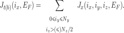
Here, the layer filter considered is a slab with size Nx × Ny × Nz [Fig. 1(a)], Jx(ix, iy, iz, EF) is the x component of the local current on site (ix, iy, iz) under bias V and Jt (Jb) represents the transmission current near the top (bottom) layer. We numerically calculate the transmission current J = Jt + Jb and layer polarization P versus chemical potential μ of the central region, where μ = EF − E0 measures the difference between EF and the energy of the Dirac point E0 [red line with open squares and blue line with filled squares in Fig. 1(b)]. In the gap of the surface states, J = e2V/h is quantized, meaning that the filtering process is dissipationless and the transmission current becomes fully layer polarized on the drain terminal with P = +1. We further calculate the local current distribution to visualize the layer polarization. As shown in Fig. 1(c), the layer filter only permits the top layer current (indicated by the blue arrows), blocking the bottom layer current, so we call it the top layer filter (TLF). Similarly, we can also obtain the bottom layer filter (BLF) by simply reversing the source and drain. The transmission current J and polarization P [Fig. 1(b)] show that inside the gap, the transmission current is still quantized (J = e2V/h), but fully layer polarized with P = −1. The local current distribution also verifies that the current only goes through the bottom surface, as shown in Fig. 1(d). The layer polarization of the current can be detected through the scanning microwave impedance microscopy images. The measured current signal on the top layer of  for the TLF will be much stronger than that for the BLF, although the conductances for the two cases are both quantized [54,55,84].
The performance of electronic devices is usually suppressed by disorders [24,32]. Here, we show that the efficiency of the layer filter is robust against weak disorders. We introduce a random on-site potential term Hdis = U(r)s0 ⊗ σ0, where U(r) is a local potential uniformly distributed within [−W/2, W/2]. The differential conductance G = J/V and layer polarization P of the TLF versus μ and disorder strength W are plotted in Fig. 2. For small W, G remains quantized and the current remains fully polarized (P = 1) for a μ window. By increasing W, the μ window with quantized G for the TLF shrinks, but still survives under strong disorder strength (such as W = 1; see Fig. 2) due to the robustness of the topologically protected chiral DW modes.
Figure 2.

(a and b) G and P of the TLF as functions of μ and W. Other parameters are the same as in Fig. 1.
Though the key physics are captured by the model study, more realistic considerations can facilitate the experimental realization of the layer filter; see the online supplementary material. Calculations using realistic material parameters of  show that an ideal DW (DW width WD = 0) can act as a filter when EF is inside the surface gap (≈2Mz = 0.08 eV). The finite width of the DW can induce trivial one-dimensional sub-bands, of which the gap is proportional to 1/WD and may lie within the surface gap. Nevertheless, as we estimated using realistic material parameters, a sub-band gap larger than 10 meV can be observed for WD ≈ 500 nm, which is able to be distinguished by current transport experiments. Moreover, the non-uniformity, the different spin-flop structure as well as the curved shape of the DWs have little influence on the quantized transport of the layer filter; see the online supplementary material. Therefore, the dissipationless transport G = e2/h and the full layer polarization P = ±1, are robust against the irregularity of the DWs in
  . Axion insulators have also been observed in topological insulators with magnetization deposited only on the top and bottom surfaces [85,86]. Our proposed layertronic devices can also be constructed by introducing domain walls in these systems.
Layer valve
The layer valve device serves as a switch to turn ‘on’ or ‘off’ the specific layer-polarized current. It is designed by connecting the TLF and BLF sequentially from left to right as sketched in Fig. 3(a). We denote by μL (μR) the chemical potential of the TLF (BLF) in the top (bottom) part of the valve. Panels (b) and (c) of Fig. 3 show that the layer-resolved currents Jt and Jb [versus μL(μR) of the TLF (BLF)] both vanish in the gap of the surface states, indicating zero transmission current. The layer valve is in the ‘off’ status. This can be ascribed to the opposite chirality of the DW modes in the TLF and BLF [Fig. 3(a)]. The chirality reversal turns off the valve by blocking the transmission current on both the top and bottom layers. When we independently shift μL(μR) to the surface states, the layer valve is turned ‘on’ and generates current with bottom (top) layer polarization. As shown in Fig. 3(b), by shifting μL, Jb increases while Jt remains at zero, indicating that the valve is turned on and works as a BLF. Similarly, when μR is tuned such that EF locates deeply inside the surface states, Jb remains small while Jt becomes significantly large [Fig. 3(c)], which implies that the valve is turned on as a TLF. Moreover, the quantized transport of Jb and Jt is better for thicker valves [see the curves in Fig. 3(b) and (c) with Nz = 6 and Nz = 10], which originate from the suppression of the backscattering between spatially separated DW modes.
Figure 3.

(a) Top panel: schematic of the layer valve. The DWs are separated by D in units of the lattice constant a. Bottom panel: the domain structure required by the layer valve can be realized in a gate-controlled way under a perpendicular magnetic field B [33]. (b and c) Layer-resolved currents Jt and Jb of the valve versus the TLF (BLF) chemical potential μL (μR), with fixed μR = 0.02 (μL = 0.02) of the BLF (TLF), respectively. (d and e) The transmission current J = Jt + Jb in the presence of disorders versus μL (μR = 0.02) for different (d) W and (e) D. Model parameters are Ny = 50,  and the terminal chemical potential is 0.25.
The performance of the layer valve is also robust against disorders. As shown in Fig. 3(d), when μL is tuned such that EF lies inside the gap of the TLF and W < 0.5, J slightly deviates from zero, indicating that the layer valve is robust against weak disorders. For strong disorders, e.g. W = 1, J climbs up, leading to the reduction in the on off ratio. This stems from the scattering of DW modes in the TLF to that in the BLF under disorders. However, the on:off ratio can be significantly enhanced by separating the DW in the TLF and BLF further [increasing D; see Fig. 3(a)], which suppresses the scattering. In Fig. 3(e), J reduces as D increases; thus, the on off ratio rises accordingly. For spintronics/valleytronics, disorder induces large scattering between opposite spin/valley components, which greatly suppresses the on off ratio of the spin/valley valve [17,87]. In layertronics, besides the topologically protected chiral DW modes, the high performance of layer valve under disorder is also ensured by the spatially resolved layer degree of freedom. These transport properties are also verified by using realistic material parameters of  ; see the online supplementary material.
Experimentally, the layer valve can be achieved in a gate-controlled way. As shown in Fig. 3(a), under a perpendicular magnetic field B, the applied gate voltages on the four split gates induce alternative electric field E, giving rise to the domain structure of the AFM order due to  of the AI. Therefore, the layer valve devices with high on off ratio are experimentally feasible.
Layer reverser
In applications, one expects that the binary bits stored inside the logical unit could be switched easily. However, switching internal degrees of freedom of electrons is challenging in experiments, especially for spintronics and valleytronics. An example is that the Datta–Das transistor [62–64], the reverser of the spin degrees of freedom of electrons, has not been completely realized and applied since its first proposal. A similar dilemma appears in valleytronics where an efficient valley reverser is hard to design. Interestingly, the feasibility of tuning the AFM AI  into the FM-CI phase facilitates the layer reverser device, which inverts the layer degree of freedom dissipationlessly. As sketched in Fig. 4(a) and (b), the reverser consists of an FM-CI domain sandwiched by two AFM AIs with different AFM orders, which can be achieved experimentally by applying a vertical magnetic field on
  to reform the magnetization alignment [36,50].
Figure 4.

Schematics of top-bottom (a) and bottom-top (b) layer reversers. Colored arrows mark the layer reversing of the transmission modes. Terminals 3 and 4 are metallic contacts on the top surface. (c and d) Local current distributions of the two kinds of reversers (Nz = 30), with μ = 0.02. (e) Differential conductance between terminals 1 and 2 of the top-bottom reverser  and the bottom-top reverser
  versus μ with terminals 3 and 4 floated. (f) Local resistances of the top-bottom reverser versus μ. Model parameters are Ny = 108, Nx = 60, the terminal chemical potential is 0.2 and the sizes of contacts 3 and 4 are 8 × 8.
The key ingredient that triggers layer reversing is the layer-crossing chiral edge mode, which starts from the top/bottom surface, goes through the CI edge mode on the side surface, then flows back into the bottom/top surface. The local current distributions [Fig. 4(c)] show that the top layer current is inverted to the bottom layer. We denote such a reverser as a top-bottom layer reverser. Similarly, the bottom-top reverser is realized by simply reversing the AFM order of the AIs [33] [Fig. 4(b) and (d)]. The dissipationless nature of the layer reverser is reflected by the quantization of the conductances between terminals 1 and 2  and
and  for the two kinds of reversers. As shown in Fig. 4(e), in the gap of the surface states,
  and
and  are nearly quantized (e2/h). As the thickness Nz grows from 10 to 30,
  and
and  are better quantized due to the suppression of the backscattering between two DW modes.
Experimentally, the reversal of layer polarization, as well as the information encoded by the layer degree of freedom, can be detected through the layer-resolved transport measurements. It can be achieved by attaching two additional point contacts (terminal 3 and 4) at the DWs on the top surface [Fig. 4(a–b)], and measuring the resistances between different pairs of terminals. As shown in Fig. 4(f), for the top-bottom reverser, colossal local resistances  and
and  appear around μ = 0 because of the absence of the transmission mode that connects terminal 4 with the others. In contrast, resistances
  and
and  are quantized h/e2 because of the chiral mode that connects terminals 1 and 2 or 1 and 3.
CONCLUSIONS
We introduced the layertronics and designed key devices utilizing the layer degree of freedom of the AFM AI  . The corresponding layer filter, layer valve devices were constructed based on the AFM-DW modes. The layer reverser device, which circumvents the difficulties in constructing reversers in spintronics and valleytronics, can be achieved through the FM-CI phase of
  . The requirements for realizing layertronics are achievable under state-of-the-art experimental conditions. The robustness of DW modes under disorders realizes dissipationless manipulation of the layer degree of freedom, making layertronics a promising paradigm in constructing a new generation of electronic devices.
Supplementary Material
which contain simulations with realistic material parameters and the proposal of realizing layertronic devices in a gate-controlled way, and include [69,88–97].
ACKNOWLEDGEMENTS
We thank Weida Wu, Jian Shen, Fengqi Song, Yijia Wu and Zhiqiang Zhang for fruitful discussions.
Contributor Information
Shuai Li, School of Physical Science and Technology, Soochow University, Suzhou 215006, China; Institute for Advanced Study, Soochow University, Suzhou 215006, China.
Ming Gong, International Center for Quantum Materials, School of Physics, Peking University, Beijing 100871, China.
Shuguang Cheng, Department of Physics, Northwest University, Xi’an 710069, China.
Hua Jiang, Institute for Advanced Study, Soochow University, Suzhou 215006, China; Interdisciplinary Center for Theoretical Physics and Information Sciences, Fudan University, Shanghai 200433, China.
X C Xie, International Center for Quantum Materials, School of Physics, Peking University, Beijing 100871, China; Interdisciplinary Center for Theoretical Physics and Information Sciences, Fudan University, Shanghai 200433, China; Hefei National Laboratory, Hefei 230088, China.
FUNDING
This work is financially supported by the National Key R&D Program of China (2019YFA0308403 and 2022YFA1403700), the Strategic Priority Research Program of the Chinese Academy of Sciences (XDB28000000) and the National Natural Science Foundation of China (11822407 and 11874298).
AUTHOR CONTRIBUTIONS
H.J. and M.G. proposed the project from a discussion with X.-C.X.; S.L. and M.G. carried out the numerical calculations; H.J. and X.-C.X. supervised the project. All authors were involved in analyzing the data and writing the manuscript.
Conflict of interest statement. None declared.
REFERENCES
- 1. Riordan M, Hoddeson L, Herring C. The invention of the transistor. Rev Mod Phys 1999; 71: S336–45. 10.1103/RevModPhys.71.S336 [DOI] [Google Scholar]
- 2. Recher P, Sukhorukov EV, Loss D. Quantum dot as spin filter and spin memory. Phys Rev Lett 2000; 85: 1962–5. 10.1103/PhysRevLett.85.1962 [DOI] [PubMed] [Google Scholar]
- 3. Grundler D. Ballistic spin-filter transistor. Phys Rev B 2001; 63: 161307(R). 10.1103/PhysRevB.63.161307 [DOI] [Google Scholar]
- 4. Wang B, Wang J, Guo H. Quantum spin field effect transistor. Phys Rev B 2003; 67: 092408. 10.1103/PhysRevB.67.092408 [DOI] [Google Scholar]
- 5. Jiang S, Li L, Wang Z et al. Spin tunnel field-effect transistors based on two-dimensional van der Waals heterostructures. Nat Electron 2019; 2: 159–63. 10.1038/s41928-019-0232-3 [DOI] [Google Scholar]
- 6. Tombros N, Jozsa C, Popinciuc M et al. Electronic spin transport and spin precession in single graphene layers at room temperature. Nature 2007; 448: 571–4. 10.1038/nature06037 [DOI] [PubMed] [Google Scholar]
- 7. Žutić I, Fabian J, Das Sarma S. Spintronics: fundamentals and applications. Rev Mod Phys 2004; 76: 323–410. 10.1103/RevModPhys.76.323 [DOI] [Google Scholar]
- 8. Fert A. Nobel lecture: origin, development, and future of spintronics. Rev Mod Phys 2008; 80: 1517–30. 10.1103/RevModPhys.80.1517 [DOI] [PubMed] [Google Scholar]
- 9. Han W, Pi K, McCreary KM et al. Tunneling spin injection into single layer graphene. Phys Rev Lett 2010; 105: 167202. 10.1103/PhysRevLett.105.167202 [DOI] [PubMed] [Google Scholar]
- 10. Han W, Kawakami RK, Gmitra M et al. Graphene spintronics. Nat Nanotechnol 2014; 9: 794–807. 10.1038/nnano.2014.214 [DOI] [PubMed] [Google Scholar]
- 11. Linder J, Robinson JWA. Superconducting spintronics. Nat Phys 2015; 11: 307–15. 10.1038/nphys3242 [DOI] [Google Scholar]
- 12. Urdampilleta M, Klyatskaya S, Cleuziou JP et al. Supramolecular spin valves. Nat Mater 2011; 10: 502–6. 10.1038/nmat3050 [DOI] [PubMed] [Google Scholar]
- 13. Tao LL, Tsymbal EY. Two-dimensional spin-valley locking spin valve. Phys Rev B 2019; 100: 161110(R). 10.1103/PhysRevB.100.161110 [DOI] [Google Scholar]
- 14. S̆mejkal L, Mokrousov Y, Yan B et al. Topological antiferromagnetic spintronics. Nat Phys 2018; 14: 242–51. 10.1038/s41567-018-0064-5 [DOI] [Google Scholar]
- 15. Rycerz A, Tworzydlo J, Beenakker CWJ. Valley filter and valley valve in graphene. Nat Phys 2007; 3: 172–5. 10.1038/nphys547 [DOI] [Google Scholar]
- 16. Xiao D, Yao W, Niu Q. Valley-contrasting physics in graphene: magnetic moment and topological transport. Phys Rev Lett 2007; 99: 236809. 10.1103/PhysRevLett.99.236809 [DOI] [PubMed] [Google Scholar]
- 17. Akhmerov AR, Bardarson JH, Rycerz A et al. Theory of the valley-valve effect in graphene nanoribbons. Phys Rev B 2008; 77: 205416. 10.1103/PhysRevB.77.205416 [DOI] [Google Scholar]
- 18. Jung J, Zhang F, Qiao Z et al. Valley-Hall kink and edge states in multilayer graphene. Phys Rev B 2011; 84: 075418. 10.1103/PhysRevB.84.075418 [DOI] [Google Scholar]
- 19. Qiao Z, Jung J, Niu Q et al. Electronic highways in bilayer graphene. Nano Lett 2011; 11: 3453–9. 10.1021/nl201941f [DOI] [PubMed] [Google Scholar]
- 20. Zhang F, Jung J, Fiete GA et al. Spontaneous quantum Hall states in chirally stacked few-layer graphene systems. Phys Rev Lett 2011; 106: 156801. 10.1103/PhysRevLett.106.156801 [DOI] [PubMed] [Google Scholar]
- 21. Gunlycke D, White CT. Graphene valley filter using a line defect. Phys Rev Lett 2011; 106: 136806. 10.1103/PhysRevLett.106.136806 [DOI] [PubMed] [Google Scholar]
- 22. Cai T, Yang SA, Li X et al. Magnetic control of the valley degree of freedom of massive Dirac fermions with application to transition metal dichalcogenides. Phys Rev B 2013; 88: 115140. 10.1103/PhysRevB.88.115140 [DOI] [Google Scholar]
- 23. Pan H, Li X, Zhang F et al. Perfect valley filter in a topological domain wall. Phys Rev B 2015; 92: 041404(R). 10.1103/PhysRevB.92.041404 [DOI] [Google Scholar]
- 24. Cheng SG, Zhou J, Jiang H et al. The valley filter efficiency of monolayer graphene and bilayer graphene line defect model. New J Phys 2016; 18: 103024. 10.1088/1367-2630/18/10/103024 [DOI] [Google Scholar]
- 25. Zhou T, Cheng S, Schleenvoigt M et al. Quantum spin-valley Hall kink states: from concept to materials design. Phys Rev Lett 2021; 127: 116402. 10.1103/PhysRevLett.127.116402 [DOI] [PubMed] [Google Scholar]
- 26. Lee J, Mak KF, Shan J. Electrical control of the valley Hall effect in bilayer MoS2 transistors. Nat Nanotechnol 2016; 11: 421–5. 10.1038/nnano.2015.337 [DOI] [PubMed] [Google Scholar]
- 27. Huai Y, Anderson G, Pakala M. IrMn based spin-filter spin-valves. J Appl Phys 2000; 87: 5741–3. 10.1063/1.372507 [DOI] [Google Scholar]
- 28. Song Y, Dai G. Spin filter and spin valve in ferromagnetic graphene. Appl Phys Lett 2015; 106: 223104. 10.1063/1.4921668 [DOI] [Google Scholar]
- 29. Koo HC, Kwon JH, Eom J et al. Control of spin precession in a spin-injected field effect transistor. Science 2009; 325: 1515–8. 10.1126/science.1173667 [DOI] [PubMed] [Google Scholar]
- 30. Li J, Zhang RX, Yin Z et al. A valley valve and electron beam splitter. Science 2018; 362: 1149–52. 10.1126/science.aao5989 [DOI] [PubMed] [Google Scholar]
- 31. Rasolt M, Halperin BI, Vanderbilt D. Dissipation due to a “valley wave” channel in the quantum Hall effect of a multivalley semiconductor. Phys Rev Lett 1986; 57: 126–9. 10.1103/PhysRevLett.57.126 [DOI] [PubMed] [Google Scholar]
- 32. An XT, Xiao J, Tu MWY et al. Realization of valley and spin pumps by scattering at nonmagnetic disorders. Phys Rev Lett 2017; 118: 096602. 10.1103/PhysRevLett.118.096602 [DOI] [PubMed] [Google Scholar]
- 33. Gao A, Liu YF, Hu C et al. Layer Hall effect in a 2D topological axion antiferromagnet. Nature 2021; 595: 521–5. 10.1038/s41586-021-03679-w [DOI] [PubMed] [Google Scholar]
- 34. Lee W, Fernandez-Mulligan S, Tan H et al. Layer-by-layer disentanglement of Bloch states. Nat Phys 2023; 1–6. 10.1038/s41567-023-02008-4 [DOI] [Google Scholar]
- 35. Zhai D, Chen C, Xiao C et al. Time-reversal even charge Hall effect from twisted interface coupling. Nat Commun 2023; 14: 1961. 10.1038/s41467-023-37644-0 [DOI] [PMC free article] [PubMed] [Google Scholar]
- 36. Liu C, Wang Y, Li H et al. Robust axion insulator and Chern insulator phases in a two-dimensional antiferromagnetic topological insulator. Nat Mater 2020; 19: 522–7. 10.1038/s41563-019-0573-3 [DOI] [PubMed] [Google Scholar]
- 37. Sun HP, Li CA, Choi SJ et al. Magnetic topological transistor exploiting layer-selective transport. Phys Rev Res 2023; 5: 013179. 10.1103/PhysRevResearch.5.013179 [DOI] [Google Scholar]
- 38. Chen R, Sun HP, Gu M et al. Layer Hall effect induced by hidden Berry curvature in antiferromagnetic insulators. Natl Sci Rev 2022, doi: 10.1093/nsr/nwac140. 10.1093/nsr/nwac140 [DOI] [PMC free article] [PubMed] [Google Scholar]
- 39. Peng R, Zhang T, He Z et al. Intrinsic layer-polarized anomalous Hall effect in bilayer MnBi2Te4. Phys Rev B 2023; 107: 085411. 10.1103/PhysRevB.107.085411 [DOI] [Google Scholar]
- 40. Lee SH, Zhu Y, Wang Y et al. Spin scattering and noncollinear spin structure-induced intrinsic anomalous Hall effect in antiferromagnetic topological insulator MnBi2Te4. Phys Rev Res 2019; 1: 012011. 10.1103/PhysRevResearch.1.012011 [DOI] [Google Scholar]
- 41. Zhang D, Shi M, Zhu T et al. Topological axion states in the magnetic insulator MnBi2Te4 with the quantized magnetoelectric effect. Phys Rev Lett 2019; 122: 206401. 10.1103/PhysRevLett.122.206401 [DOI] [PubMed] [Google Scholar]
- 42. Otrokov MM, Klimovskikh II, Bentmann H et al. Prediction and observation of an antiferromagnetic topological insulator. Nature 2019; 576: 416–22. 10.1038/s41586-019-1840-9 [DOI] [PubMed] [Google Scholar]
- 43. Li J, Li Y, Du S et al. Intrinsic magnetic topological insulators in van der Waals layered MnBi2Te4-family materials. Sci Adv 2019; 5: eaaw5685. 10.1126/sciadv.aaw5685 [DOI] [PMC free article] [PubMed] [Google Scholar]
- 44. Otrokov MM, Rusinov IP, Blanco-Rey M et al. Unique thickness-dependent properties of the van der Waals interlayer antiferromagnet MnBi2Te4 films. Phys Rev Lett 2019; 122: 107202. 10.1103/PhysRevLett.122.107202 [DOI] [PubMed] [Google Scholar]
- 45. Sass PM, Ge W, Yan J et al. Magnetic imaging of domain walls in the antiferromagnetic topological insulator MnBi2Te4. Nano Lett 2020; 20: 2609–14. 10.1021/acs.nanolett.0c00114 [DOI] [PubMed] [Google Scholar]
- 46. Li J, Wang C, Zhang Z et al. Magnetically controllable topological quantum phase transitions in the antiferromagnetic topological insulator MnBi2Te4. Phys Rev B 2019; 100: 121103(R). 10.1103/PhysRevB.100.121103 [DOI] [Google Scholar]
- 47. Deng Y, Yu Y, Shi MZ et al. Quantum anomalous Hall effect in intrinsic magnetic topological insulator MnBi2Te4. Science 2020; 367: 895–900. 10.1126/science.aax8156 [DOI] [PubMed] [Google Scholar]
- 48. Zhang S, Wang R, Wang X et al. Experimental observation of the gate-controlled reversal of the anomalous Hall effect in the intrinsic magnetic topological insulator MnBi2Te4 device. Nano Lett 2020; 20: 709–14. 10.1021/acs.nanolett.9b04555 [DOI] [PubMed] [Google Scholar]
- 49. Zhao YF, Zhou LJ, Wang F et al. Even–odd layer-dependent anomalous Hall effect in topological magnet MnBi2Te4 thin films. Nano Lett 2021; 21: 7691–8. 10.1021/acs.nanolett.1c02493 [DOI] [PubMed] [Google Scholar]
- 50. Ge J, Liu Y, Wang P et al. Magnetization-tuned topological quantum phase transition in MnBi2Te4 devices. Phys Rev B 2022; 105: L201404. 10.1103/PhysRevB.105.L201404 [DOI] [Google Scholar]
- 51. He QL, Hughes TL, Armitage NP et al. Topological spintronics and magnetoelectronics. Nat Mater 2022; 21: 15–23. 10.1038/s41563-021-01138-5 [DOI] [PubMed] [Google Scholar]
- 52. Zhang Z, Wang N, Cao N et al. Controlled large non-reciprocal charge transport in an intrinsic magnetic topological insulator MnBi2Te4. Nat Commun 2022; 13: 6191. 10.1038/s41467-022-33705-y [DOI] [PMC free article] [PubMed] [Google Scholar]
- 53. Yasuda K, Mogi M, Yoshimi R et al. Quantized chiral edge conduction on domain walls of a magnetic topological insulator. Science 2017; 358: 1311–4. 10.1126/science.aan5991 [DOI] [PubMed] [Google Scholar]
- 54. Lin W, Feng Y, Wang Y et al. Direct visualization of edge state in even-layer MnBi2Te4 at zero magnetic field. Nat Commun 2022; 13: 7714. 10.1038/s41467-022-35482-0 [DOI] [PMC free article] [PubMed] [Google Scholar]
- 55. Lin W, Feng Y, Wang Y et al. Influence of the dissipative topological edge state on quantized transport in MnBi2Te4. Phys Rev B 2022; 105: 165411. 10.1103/PhysRevB.105.165411 [DOI] [Google Scholar]
- 56. Xu HK, Gu M, Fei F et al. Observation of magnetism-induced topological edge state in antiferromagnetic topological insulator MnBi4Te7. ACS Nano 2022; 16: 9810–8. 10.1021/acsnano.2c03622 [DOI] [PubMed] [Google Scholar]
- 57. Garrity KF, Chowdhury S, Tavazza FM. Topological surface states of MnBi2Te4 at finite temperatures and at domain walls. Phys Rev Mater 2021; 5: 024207. 10.1103/PhysRevMaterials.5.024207 [DOI] [Google Scholar]
- 58. Alfonsov A, Facio JI, Mehlawat K et al. Strongly anisotropic spin dynamics in magnetic topological insulators. Phys Rev B 2021; 103: L180403. 10.1103/PhysRevB.103.L180403 [DOI] [Google Scholar]
- 59. Rusinov IP, Men’shov VN, Chulkov EV. Spectral features of magnetic domain walls on the surface of three-dimensional topological insulators. Phys Rev B 2021; 104: 035411. 10.1103/PhysRevB.104.035411 [DOI] [Google Scholar]
- 60. Petrov EK, Men’shov VN, Rusinov IP et al. Domain wall induced spin-polarized flat bands in antiferromagnetic topological insulators. Phys Rev B 2021; 103: 235142. 10.1103/PhysRevB.103.235142 [DOI] [Google Scholar]
- 61. Xiao C, Tang J, Zhao P et al. Chiral channel network from magnetization textures in two-dimensional MnBi2Te4. Phys Rev B 2020; 102: 125409. 10.1103/PhysRevB.102.125409 [DOI] [Google Scholar]
- 62. Datta S, Das B. Electronic analog of the electro-optic modulator. Appl Phys Lett 1990; 56: 665–7. 10.1063/1.102730 [DOI] [Google Scholar]
- 63. Egues JC, Burkard G, Loss D. Datta–Das transistor with enhanced spin control. Appl Phys Lett 2003; 82: 2658–60. 10.1063/1.1564867 [DOI] [Google Scholar]
- 64. Sarkar K, Aharony A, Entin-Wohlman O et al. Effects of magnetic fields on the Datta-Das spin field-effect transistor. Phys Rev B 2020; 102: 115436. 10.1103/PhysRevB.102.115436 [DOI] [Google Scholar]
- 65. Li H, Jiang H, Chen CZ et al. Critical behavior and universal signature of an axion insulator state. Phys Rev Lett 2021; 126: 156601. 10.1103/PhysRevLett.126.156601 [DOI] [PubMed] [Google Scholar]
- 66. Zhang H, Liu CX, Qi XL et al. Topological insulators in Bi2Se3, Bi2Te3 and Sb2Te3 with a single Dirac cone on the surface. Nat Phys 2009; 5: 438–42. 10.1038/nphys1270 [DOI] [Google Scholar]
- 67. Liu CX, Qi XL, Zhang H et al. Model Hamiltonian for topological insulators. Phys Rev B 2010; 82: 045122. 10.1103/PhysRevB.82.045122 [DOI] [Google Scholar]
- 68. Zhang RX, Wu F, Das Sarma S. Möbius insulator and higher-order topology in MnBi2nTe3n+1. Phys Rev Lett 2020; 124: 136407. 10.1103/PhysRevLett.124.136407 [DOI] [PubMed] [Google Scholar]
- 69. Chen R, Li S, Sun HP et al. Using nonlocal surface transport to identify the axion insulator. Phys Rev B 2021; 103: L241409. 10.1103/PhysRevB.103.L241409 [DOI] [Google Scholar]
- 70. Ji HR, Liu YZ, Wang H et al. Detection of magnetic gap in topological surface states of MnBi2Te4. Chin Phys Lett 2021; 38: 107404. 10.1088/0256-307X/38/10/107404 [DOI] [Google Scholar]
- 71. Zeugner A, Nietschke F, Wolter AUB et al. Chemical aspects of the candidate antiferromagnetic topological insulator MnBi2Te4. Chem Mater 2019; 31: 2795–806. 10.1021/acs.chemmater.8b05017 [DOI] [Google Scholar]
- 72. Liu M, Lei C, Kim H et al. Visualizing the interplay of Dirac mass gap and magnetism at nanoscale in intrinsic magnetic topological insulators. Proc Natl Acad Sci 2022; 119: e2207681119. 10.1073/pnas.2207681119 [DOI] [PMC free article] [PubMed] [Google Scholar]
- 73. Chu RL, Shi J, Shen SQ. Surface edge state and half-quantized Hall conductance in topological insulators. Phys Rev B 2011; 84: 085312. 10.1103/PhysRevB.84.085312 [DOI] [Google Scholar]
- 74. Varnava N, Vanderbilt D. Surfaces of axion insulators. Phys Rev B 2018; 98: 245117. 10.1103/PhysRevB.98.245117 [DOI] [Google Scholar]
- 75. Qi XL, Hughes TL, Zhang SC. Topological field theory of time-reversal invariant insulators. Phys Rev B 2008; 78: 195424. 10.1103/PhysRevB.78.195424 [DOI] [Google Scholar]
- 76. Essin AM, Moore JE, Vanderbilt D. Magnetoelectric polarizability and axion electrodynamics in crystalline insulators. Phys Rev Lett 2009; 102: 146805. 10.1103/PhysRevLett.102.146805 [DOI] [PubMed] [Google Scholar]
- 77. Sekine A, Nomura K. Axion electrodynamics in topological materials. J Appl Phys 2021; 129: 141101. 10.1063/5.0038804 [DOI] [Google Scholar]
- 78. Zhou H, Li H, Xu DH et al. Transport theory of half-quantized Hall conductance in a semi-magnetic topological insulator. Phys Rev Lett 2022; 129: 096601. [DOI] [PubMed] [Google Scholar]
- 79. Gong M, Liu H, Jiang H et al. Half-quantized helical hinge currents in axion insulators. Natl Sci Rev 2023; 10: nwad025. 10.1093/nsr/nwad025 [DOI] [PMC free article] [PubMed] [Google Scholar]
- 80. Chiu CK, Teo JCY, Schnyder AP et al. Classification of topological quantum matter with symmetries. Rev Mod Phys 2016; 88: 035005. 10.1103/RevModPhys.88.035005 [DOI] [Google Scholar]
- 81. Callan C, Harvey J. Anomalies and fermion zero modes on strings and domain walls. Nuclear Physics B 1985; 250: 427–36. 10.1016/0550-3213(85)90489-4 [DOI] [Google Scholar]
- 82. Ju L, Shi Z, Nair N et al. Topological valley transport at bilayer graphene domain walls. Nature 2015; 520: 650–5. 10.1038/nature14364 [DOI] [PubMed] [Google Scholar]
- 83. Qiu JX, Tzschaschel C, Ahn J et al. Axion optical induction of antiferromagnetic order. Nat Mater 2023; 22: 583–90. 10.1038/s41563-023-01493-5 [DOI] [PubMed] [Google Scholar]
- 84. Feng Y, Zhu J, Lin W et al. Helical luttinger liquid on the edge of a two-dimensional topological antiferromagnet. Nano Lett 2022; 22:7606–14. 10.1021/acs.nanolett.2c02701 [DOI] [PubMed] [Google Scholar]
- 85. Mogi M, Kawamura M, Yoshimi R et al. A magnetic heterostructure of topological insulators as a candidate for an axion insulator. Nat Mater 2017; 16: 516–21. 10.1038/nmat4855 [DOI] [PubMed] [Google Scholar]
- 86. Xiao D, Jiang J, Shin JH et al. Realization of the axion insulator state in quantum anomalous Hall sandwich heterostructures. Phys Rev Lett 2018; 120: 056801. 10.1103/PhysRevLett.120.056801 [DOI] [PubMed] [Google Scholar]
- 87. Averkiev NS, Golub LE. Giant spin relaxation anisotropy in zinc-blende heterostructures. Phys Rev B 1999; 60: 15582–4. 10.1103/PhysRevB.60.15582 [DOI] [Google Scholar]
- 88. Sass PM, Kim J, Vanderbilt D et al. Robust A-type order and spin-flop transition on the surface of the antiferromagnetic topological insulator MnBi2Te4. Phys Rev Lett 2020; 125: 037201. 10.1103/PhysRevLett.125.037201 [DOI] [PubMed] [Google Scholar]
- 89. Yang Y, Jia Z, Wu Y et al. Gapped topological kink states and topological corner states in honeycomb lattice. Sci Bull 2020; 65: 531–7. 10.1016/j.scib.2020.01.024 [DOI] [PubMed] [Google Scholar]
- 90. Bernevig BA, Hughes TL, Zhang SC. Quantum spin Hall effect and topological phase transition in HgTe quantum wells. Science 2006; 314: 1757–61. 10.1126/science.1133734 [DOI] [PubMed] [Google Scholar]
- 91. König M, Wiedmann S, Brüne C et al. Quantum spin Hall insulator state in HgTe quantum wells. Science 2007; 318: 766–70. 10.1126/science.1148047 [DOI] [PubMed] [Google Scholar]
- 92. Chen G, Zhu J, Quesada A et al. Novel chiral magnetic domain wall structure in Fe/Ni/Cu(001) films. Phys Rev Lett 2013; 110: 177204. 10.1103/PhysRevLett.110.177204 [DOI] [PubMed] [Google Scholar]
- 93. Chen G, Ma T, N’Diaye AT et al. Tailoring the chirality of magnetic domain walls by interface engineering. Nat Commun 2013; 4: 2671. 10.1038/ncomms3671 [DOI] [PubMed] [Google Scholar]
- 94. Zhou YF, Hou Z, Sun QF. Configuration-sensitive transport at the domain walls of a magnetic topological insulator. Phys Rev B 2018; 98: 165433. 10.1103/PhysRevB.98.165433 [DOI] [Google Scholar]
- 95. Li J, Wang K, McFaul KJ et al. Gate-controlled topological conducting channels in bilayer graphene. Nat Nanotechnol 2016; 11: 1060–5. 10.1038/nnano.2016.158 [DOI] [PubMed] [Google Scholar]
- 96. Chen H, Zhou P, Liu J et al. Gate controlled valley polarizer in bilayer graphene. Nat Commun 2020; 11: 1202. 10.1038/s41467-020-15117-y [DOI] [PMC free article] [PubMed] [Google Scholar]
- 97. Martin I, Blanter YM, Morpurgo AF. Topological confinement in bilayer graphene. Phys Rev Lett 2008; 100: 036804. 10.1103/PhysRevLett.100.036804 [DOI] [PubMed] [Google Scholar]
Associated Data
This section collects any data citations, data availability statements, or supplementary materials included in this article.
Supplementary Materials
which contain simulations with realistic material parameters and the proposal of realizing layertronic devices in a gate-controlled way, and include [69,88–97].