Abstract
A design and fabrication technique for making high-precision and large-format multifaceted mapping mirrors is presented. The method is based on two-photon polymerization, which allows more flexibility in the mapping mirror design. The mirror fabricated in this paper consists of 36 2D tilted square pixels, instead of the continuous facet design used in diamond cutting. The paper presents a detailed discussion of the fabrication parameters and optimization process, with particular emphasis on the optimization of stitching defects by compensating for the overall tilt angle and reducing the printing field of view. The fabricated mirrors were coated with a thin layer of aluminum (93 nm) using sputter coating to enhance the reflection rate over the target wave range. The mapping mirror was characterized using a white light interferometer and a scanning electron microscope, which demonstrates its optical quality surface (with a surface roughness of 12 nm) and high-precision tilt angles (with an average of 2.03% deviation). Finally, the incorporation of one of the 3D printed mapping mirrors into an image mapping spectrometer prototype allowed for the acquisition of high-quality images of the USAF resolution target and bovine pulmonary artery endothelial cells stained with three fluorescent dyes, demonstrating the potential of this technology for practical applications.
1. INTRODUCTION
Hyperspectral imaging is becoming an increasingly popular modality throughout the fields of astronomy [1–3], agriculture [4–6], biotechnology [7,8], and environment [9]. It collects spatial and spectral information from objects and generates 3D datacubes . The spectral information combined with the spatial information of objects enables robust analysis and detection algorithms. Over the past few decades, several types of these imaging spectrometers have been invented. Spectral imaging systems can be divided into three main categories: spatial scanning [10], spectral scanning [11,12], and non-scanning/snapshot [8,13–16]. This last group can be further divided into direct/field integral imaging [13,17], aperture split [17,18], image duplication through polarization/filter components, or coded computational methods such as computed tomographic imaging spectrometer (CTIS) or coded aperture snapshot spectral imaging (CASSI) [17,18]. Snapshot hyperspectral imaging systems were developed recently with the aim to detect weak signals at a relatively high frame rate because of their high light throughput [8,17–19]. In addition, snapshot imaging spectrometers do not have complicated scanning mechanisms built into the system, significantly improving stability. Therefore, they are often used in fluorescence imaging and fast-changing phenomena capture.
There are many studies about the design and fabrication of snapshot image mapping spectrometers (IMSs) [8,13,16,19,20]. The IMS uses a specially designed multifaceted mapping mirror and a matching microlens array to create void spaces between image slices on the sensor. A prism array is used to introduce dispersion to fill the void spaces with spectral information. Thus, a single capture can record both spatial and spectral information. Similar to other snapshot imaging spectrometers, IMS also requires a calibration procedure to reconstruct the 3D hyperspectral datacubes from the 2D date on the sensor. It should be noted that image quality (sampling and resolution) from IMS strongly depends on the performance of the mapping mirror [21,22]. Therefore, the design and fabrication of the mapping mirror become crucial steps. Prior mirror fabrication was based on diamond machining including raster fly cutting and ruling, while each design necessitated a unique diamond tool [21]. The specifically designed diamond tools are usually less than 100 μm wide while the length of the tools is about 2 mm long. The needle-like shape makes them extremely difficult and expensive to fabricate. Furthermore, because diamond tools are delicate, the largest permitted cutting step is under 30 μm when cutting an aluminum substrate, resulting in a time-consuming and expensive fabrication procedure. Despite it, diamond-cut mappers still have many problems, such as edge eating and facet width limitation [16,21]. Diamond tools will unavoidably cut adjacent facets that are taller than the currently cut facet because of the included angle and tilt of the tool, which is called edge eating. This phenomenon causes the variant intensity of facets, increasing the difficulty of calibration and hurting the uniformity of final images. The other problem is that the smallest tool thickness we can achieve is about 70 μm. It limits our capabilities to further increase spatial sampling.
Ongoing efforts to enhance mapping mirror quality and miniaturize its size involve the exploration of numerous new methods, including diamond turning (DT) [23] and mapper assembly with multiple stacked layers [24]. For example, mapping mirrors are divided into separate components to allow a deeper cut in the DT process. Plate stacking allows for uniform facet width and low roughness, but has limited lengths and requires semi-manual plate assembly. Both techniques require high-precision assembly. The overlap of the cutting path during DT was investigated to enable the use of wider diamond tools for narrower facets, while this technique exacerbates the problem of overcutting. As a result, it appears that none of the above approaches can successfully allow for high facet density, uniform facet width, high angular precision, and time/cost-effective manufacturability all at once.
Two-photon polymerization (2PP) is a powerful technique for creating complex 3D structures with submicrometer resolution [25,26]. Because of the small focus region generated by the two-photon femtosecond laser, the printed structure can achieve high resolution (down to 100 nm) [27,28] and optical quality roughness (less than 10 nm) [26–28]. The problems with 2PP printing, such as limited structure sizes and stitching defects, have been mitigated [29]. This makes it valuable for many applications, including micro-optics. In recent years, 2PP has been reported to successfully fabricate many optical components, including lenses [30–33] and grating/diffractive structures [34–36]. Two-photon grayscale lithography (2GL) is a mode specifically designed for the fabrication of complex 2.5 D structures with arbitrary shapes and heights. This is achieved by modulating the laser power during exposure, resulting in a gradient of the polymerization degree along the beam propagation direction [37–39]. In other words, it can vary the voxel size smoothly during printing by controlling the laser power in one layer. It relies on laser calibration based on the slicing distance, hatching distance, scanning speed, and resin properties to determine the modulation function of the laser. The calibration process requires sweeping laser power for printing test prints (micro spherical lenses) and profiling the surface to determine the optimized laser power. In contrast to traditional 2PP 3D printing, the resulting structure has a continuous variation in height and shape, rather than being composed of discrete layers as in traditional 2PP. 2GL allows for the production of high-quality curved surfaces comparable to those created using four to five times smaller hatching and slicing in traditional 2PP, without increasing the fabrication time. This makes it particularly advantageous for applications such as micro-optics, where precise control of shape and height is necessary to achieve desired optical properties.
The primary objective of this paper is to investigate the application of the 2PP technique, especially 2GL mode, for improving fabrication quality and reducing fabrication complexity of making required mapping mirrors. In particular, the focus of our study is to assess the capacity of 2PP printed mapping mirrors to achieve surface quality comparable to, or even surpassing, existing standards in terms of surface roughness and surface tilt angle precision. Additionally, we aim to explore novel design concepts that take advantage of the flexibility offered by the 2PP technique to overcome the inherent limitations of diamond-cut mapping mirrors, such as shadowing and edge eating. Finally, we also recognize the potential challenges that may arise when printing large-scale components exceeding 20 mm in size and plan to address these concerns.
In this paper, we report on the design and fabrication of multifaceted mapping mirrors using the 2PP technique. The new mapping mirrors abandon the previous continuous facet design, instead using a square-tilted pixel design. The mirror was designed as a 16-bit grayscale image in MATLAB and printed using a commercial 2PP printer in 2GL mode. To enable a reflection rate comparable to diamond-cut aluminum mapping mirrors, the mirror was sputter coated with a thin layer of aluminum (93 nm). The details of the optimization process and final printing parameters are discussed in this paper. The printed mapper was characterized using a white light interferometer and SEM to show its optical quality surface and the high-precision tilt angle for each pixel. In comparison to previous diamond-cut mappers, the new 3D printed mappers not only address most of the defects associated with the diamond-cut technique but also improve the uniformity and organization of pupil array distribution. Finally, we evaluated the imaging performance of the fabricated mapping mirror in a prototype IMS.
2. DESIGN
The multifaceted mapping mirror is a critical component of an IMS system. It is used to slice the intermediate image and to redirect light onto the microlens array. Because of its location at the intermediate image plane, it directly affects the quality of the final reconstructed images. One of the key parameters of mapping mirrors is the 2D tilt angles, which determine whether the mapped image will be collected by the exact micrometer lens as designed. Referring to the optical layout of IMS in Fig. 1(a), the tilt angles are determined by the physical positions of the micro lens and the focal length of the collection lens. For facet , the tilt angle can be calculated as
| (1) |
| (2) |
where and are tilt angles in horizontal and vertical directions, respectively; is the focal length of the collection length; and are the position of the center of the micro lens corresponding to facet .
Fig. 1.
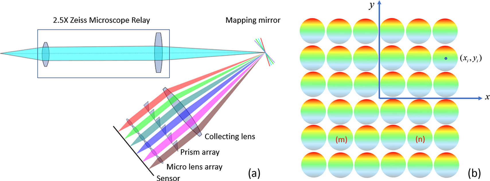
Demonstration of IMS principle. (a) Optical layout of an IMS system. (b) Schematic of a micrometer lens design.
Once the optimized tilt angles for each facet are determined, a grayscale image can be generated for the 2PP printer to process. MATLAB was used to generate the 16-bit grayscale image, and the step size was set to be 200 nm. 2D tilt angles can be converted to height values as
| (3) |
where is the thickness of the base added in the design; and are positions in horizontal and vertical directions, respectively. Furthermore, as mentioned in Section 1, the diamond-cut mapping mirrors have shadowing effects. The phenomenon is mainly because the height differences of two adjacent facets are significant. The taller facets will block light reflected from lower facets, which loses some signals of the lower facets. Reorganizing the order of these tilt angles mitigates the shadowing effect [21]. However, instead of the continuous facet design limited by the diamond-cut fabrication process, the pixel-based design can divide each facet into multiple square pixels with the same tilt angles. In this design, each facet (78 μm wide, 23 mm long) is divided into 300 78 μm × 78 μm square pixels. The DT is limited by the minimum tool width (78 μm). To have a direct comparison between the two techniques, the pixel size is set to be 78 μm × 78 μm. However, it should be noted that 2PP can fabricate smaller pixels to increase the facet density. The height differences between adjacent facets are reduced 300 times by dividing the facets into many separate pixels, which eliminates the shadowing effect. The final grayscale design is shown in Fig.2.
Fig. 2.
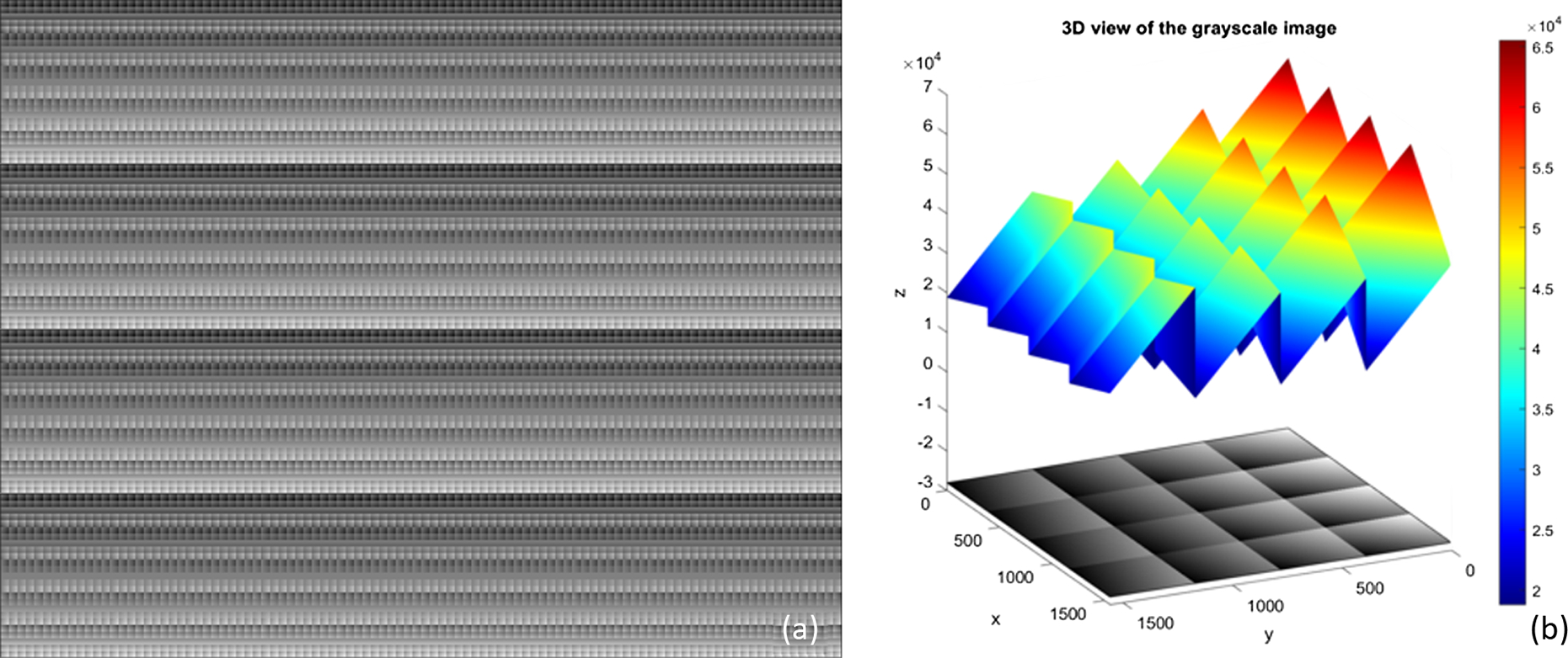
Illustration of the pixelated mapping mirror design. (a) 16-bit grayscale image of the designed mapping mirror. (b) Zoom-in 3D view of a portion of the mapping mirror.
The 2PP technique was then used to fabricate the designed mapping mirrors. From a functional application perspective, important parameters are: (1) precision of the tilt angle, less than 6% deviation required by calibration tolerance; (2) surface roughness 10–15 nm, corresponding to molded optics quality; (3) surface form λ/10, previously determined to avoid point spread function broadening; (4) uniformity of facet dimensions, less than 1%; (5) fabrication time, less than 100 h to increase reproducibility. In the study with a Nanoscribe Quantum system, we utilized the 25× objective with 0.8 NA and 780 nm laser with a maximum power of 185 mW to polymerize IP-S resin, which theoretically can achieve the parameters mentioned above. More details about the system specifications are outlined on the Nanoscribe website ([40]).
3. FABRICATION
A. 2PP Printing
The printer used in this work is a commercial 2PP printer, Quantum from Nanoscribe, Germany. The design of the mapping mirror generated from MATLAB was in 16-bit grayscale PNG image format. The image file was first loaded into the software GrayscribeX, provided together with the printer specifically for 2GL mode, for pre-processing. The pre-processing was used to set up the printing parameters and compensation. To avoid the generation of an excessively large printing file, only one column containing all the various tilts was loaded into GrayscribeX. The “tiling” feature was then applied to duplicate the signal column in the horizontal direction to form the entire mapping mirror. The final printing parameters used are shown in Table 1. Following the printing process, the sample was immersed in SU-8 developer for a duration of 18.5 min to facilitate development. Notably, it was observed that excessive development time resulted in diminished structure at the edge of the sample. To address this issue, the development time was carefully optimized in half-minute increments. The selected 18.5 min duration proved effective in completely removing the IP-S resin located on top of the structure while maintaining the quality of the printed sample. It was then washed with 99.9% isopropohyl alcohol (IPA) for 4 min.
Table 1.
List of Printing Parameters
| Objective | 25 × MF |
| Resin | IP-S |
| Slicing distance | 1 μm |
| Hatching distance | 0.2 μm |
| Scanning speed | 20,000 μm/s |
| Additional base in design | 3 μm |
| Field size x/y | 390 μm (5 pixel size) |
| Base slice count | 3 |
| Base slice distance | 1 μm |
| Base hatching distance | 0.2 μm |
| Base laser power | 45 mW |
| Base scanning speed | 20,000 μm/s |
| Shear angle | 15° |
| Interpolate | On |
All the printing and developing parameters were optimized in an iterative process. First, 9 × 9 pixel testing samples were printed to globally search for the optimized slicing distance, hatching distance, and scanning speed. The slicing distance determines the voxel size in the direction, while the hatching distance controls the scanning spacing in the plane. The hatching direction can be either or depending on the printing structure. However, in the 2GL mode, the voxel size may vary slightly by modulating the laser power if necessary to fill the design volume precisely. The parameters leading to the best surface roughness and form are 1 μm slicing distance, 0.2 μm hatching distance in the direction, and 20,000 μm/s scanning speed. The printed mapping mirror was observed under a Zygo white light interferometer (NewView 5000, Zygo, CT, USA) using 20× magnification, which is shown in Fig. 3(a). The result shows relatively good surface roughness but two main problems: flat top and deformed tail. Directly printing the structure on the substrate fully relies on the precision of the interface-finding algorithm. When the printing structure is relatively low (about 10 μm), it can impact the printing results significantly. A base was added in the software setup to improve the control of height. Additionally, a base can minimize the impact of backreflection from the printing substrate and add adhesion to the printing structure. Five different base heights (1, 2, 3, 4, and 5 μm) were tested. The surface quality indicated that when the base thickness exceeded 3 μm, there was no visible improvement by increasing the base thickness. To verify that adding a base can improve the quality of the entire mapping mirror printing, a quarter of the entire mapping mirror was printed with a 3 μm base. The selected area is shown in Fig. 3(b). The result has a sharp top, but adding a base does not fully solve the deformed tail problem. The defects still appeared at the interface between the mapping mirror structure and the base or fused silica microscope slide. Note that the printing parameters for the structure and the base were different in the 2GL mode. When the structure was printed, the printer modulated the laser power to create an adaptive laser-focusing voxel for a precise and smooth surface. However, base printing used a fixed 45 mW, which is slightly lower than the average printing laser power. The base layer may shrink more compared to the overlaying structure. Therefore, an extra base was added to the design, which is written on top of the first base. This extra base used the same printing parameters as the structure to provide a smooth transition from the base to the structure. In other words, no interface was supposed to be observed under the mapping mirror structure. The result shown in Fig. 3(c) demonstrates that the extra base did significantly improve the deformed tail. The bases have no influence on the functionality of mapping mirrors. Thus, bases were kept when integrating the mapping mirrors with an IMS prototype. However, this result provides only good single-pixel surface quality. The pixels located in the stitching area still show defectiveness. To better demonstrate how stitching defects affect the quality of final reconstructed images, it is discussed together with the 1951 USAF resolution target imaging in Section 6.
Fig. 3.
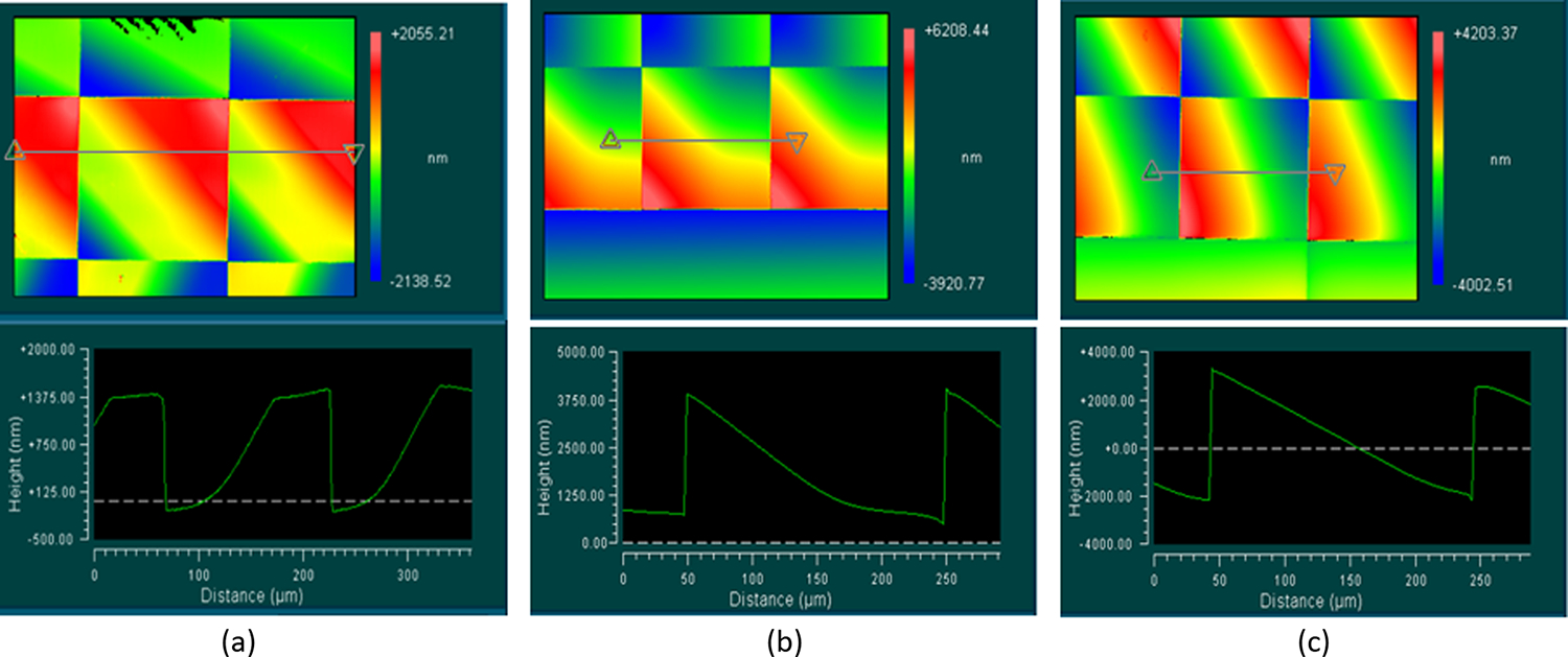
Characterization results from a Zygo white light interferometer when optimization for mapping mirror printing parameters. (a) Printing using 1 μm slicing distance and 0.2 μm hatching distance. (b) Printing with a 3 μm base added in the GrayscribeX software. (c) Printing with one 3 μm extra base added to the design.
B. Sputter Coating
After polymerization and development, the IP-S resin forms a transparent structure, which needs to be coated with a layer of aluminum to enable the functionality of mapping mirrors. The sputter coating machine (AJA ATC Orion Sputter System, MA, USA) was used to apply the aluminum coating at the Shared Equipment Authority (SEA) at Rice University. The thickness of the aluminum coating was measured to be approximately 93 nm using the Zygo white light interferometer, with less than 1% transmission rate over the visible range of 400–700 nm. Aluminum was selected because of its relatively uniform reflection over the entire target wave range. However, the coating is not limited to aluminum. When IMS systems need to be applied for short-infrared or infrared range, other materials, such as silver, copper, and gold, can also be applied. This is another advantage of the fabrication technique compared to diamond machining. Figure 4(a) displays the ultimate mapping mirror after the development process. Notably, the mapping mirrors featuring a thin aluminum layer demonstrate substantially higher reflection levels in the visible range, as presented in Fig.4(b).
Fig. 4.
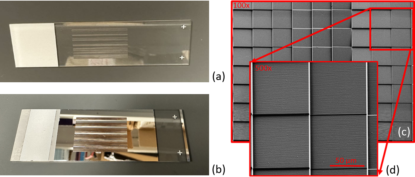
Mapping mirror fabrication results. (a) Result after laser direct writing and development. (b) Mapping mirror with a thin layer of aluminum coating. (c) Scanning electron microscope (SEM) image of a portion of a mapping mirror with repeated tilt sequence. (d) Magnified 2 × 2 mirrors. The represented distance is 50 μm as indicated by the scale bar.
4. CHARACTERIZATION
The quality of the printed mapper mirror was also assessed using the white light interferometer. In general, the printed mapping mirror consists of numerous square pixels with 36 different tilt angles, which are replicated across the entire mapping mirror. The quality of the mapping mirror can be quantified based on the primary parameters: surface roughness, form, and the accuracy of the tilt angles.
A. Surface Roughness and Form
The surface shape was measured using 50× magnification within 70 μm × 70 μm field of view (FOV). The data from the pixel with the largest tilt angle measured by the interferometer are shown in Fig. 5 as an example. As a consequence of the slightly disparate shrinkage of IP-S resin in two dimensions, pixels exhibit distinct cylindrical forms. Notably, the degree of deformation directly depends on the tilt angles, with pixels displaying greater deformations if they possess larger quantities of resin. To account for this, initial attempts were made to employ cylindrical shapes for fitting the pixel surfaces. Given the exact height of the mapper mirrors, which is less than 10 μm, the observed shrinkage is minimal, of the order of surface roughness levels. Consequently, all measured data obtained from the interferometer were directly substrated by the closest flat tilt surfaces to calculate the minimum RMS value. The mapping mirror has 36 different tilt angles in total. Two pixels from each tilt angle were selected. The RMS values of all 36 tilt angles are listed in Table 2. The average surface deviation from reference flat surfaces was 12.187 nm in a selected 70 μm × 70 μm area. The measured value can approximate surface roughness well, but it is impacted slightly by surface deformation, especially for several pixels with higher than 20 nm values in Table 2.
Fig. 5.
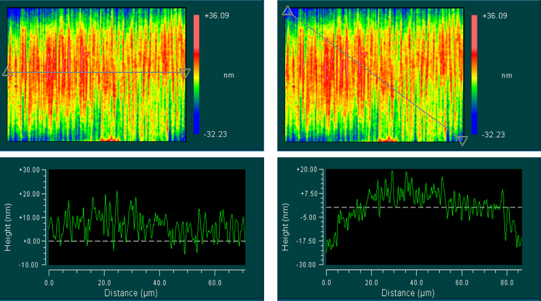
Surface roughness measurement.
Table 2.
RMS Values of Deviations from Reference Flat Surfaces for All 36 Tilt Angles
| α 1 | α 2 | α 3 | α 4 | α 5 | α 6 | |
|---|---|---|---|---|---|---|
|
| ||||||
| β 1 | 8.123 | 14.102 | 25.494 | 11.491 | 9.618 | 7.431 |
| β 2 | 9.541 | 16.709 | 21.117 | 7.222 | 5.560 | 10.623 |
| β 3 | 15.833 | 20.685 | 7.512 | 4.879 | 9.298 | 15.607 |
| β 4 | 23.753 | 8.360 | 5.717 | 8.530 | 12.858 | 28.116 |
| β 5 | 10.107 | 6.473 | 8.077 | 9.969 | 17.094 | 12.647 |
| β 6 | 6.869 | 10.948 | 16.699 | 22.766 | 8.291 | 5.954 |
The deviation between fabrication angles and design angles may result in facet image shifts on the sensor. Nevertheless, the magnitude of these shifts is inferior to those caused by any diamond-cut mapping mirror. To prevent potential signal overlap attributable to the error of fabrication angles, more void spaces than the actual size of dispersion are typically reserved. In this study, we allowed up to 5% deviations. However, considering the high precision of tilt angles from 2PP mapping mirrors, smaller void spaces can be utilized, ultimately leading to increased sensor usage.
B. Tilt Angle Precision
The measured tilt angles and deviation from the designed value are shown in Table 3. A 70.11 μm × 70.11 μm area was picked up from the center of each pixel to measure the height differences in and directions. Then Eq. (3) was applied to convert height to actual angles. As shown in Table 4, for all tilt angles in both horizontal and vertical directions, the deviation is smaller than 6% and 2.03% on average, respectively, which caused at most a 5 pixel shift on the sensor. Because 8 pixel void space was kept between each subpupil when designing the system, no cross talk was introduced due to the error of tilt angles. The fabrication result stays in the tolerance of the design.
Table 3.
Comparison of 2PP and Diamond-Cut Techniques for Mapping Mirror Fabrication
| Two-Photon Polymerization | Diamond Machining | |
|---|---|---|
|
| ||
| Fabrication time | 78 h (can be further reduced by using smaller pixels) | 2–3 weeks |
| Uniformity | 0.5% | Up to 15% |
| Spatial density | 2–3 μm | 70–80 μm |
| Precision of angles | 2.03% on average | 7.3% on average |
| Calibration difficulty | 5 images without any scanning stages | 20–2000 images with high-precision scanning stages |
| Design flexibility | Both tilt angle and pixel width adjustment | Only tilt angle adjustment in a limited range |
Table 4.
Tilt Angle Measurement and Error Analysis
| α designed value | −2.744° | −1.650° | −0.550° | 0.550° | 1.650° | 2.744° |
| α measured value | −2.811° | −1.678° | −0.582° | 0.558° | 1.655° | 2.784° |
| Deviation | −0.0640° | −0.028° | −0.0320° | 0.008° | 0.005° | 0.04° |
| Percentage deviation | −2.33% | −1.70% | −5.82% | 1.45% | 0.3% | 1.46% |
| β designed value | −2.744° | −1.650° | −0.550° | 0.550° | 1.650° | 2.744° |
| β measured value | −2.808° | −1.682° | −0.579° | 0.546° | 1.652° | 2.768° |
| Deviation | −0.0670° | −0.0320° | −0.0290° | −0.004° | 0.002° | 0.024° |
| Percentage deviation | −2.44% | −1.94% | −5.27% | −0.73% | 0.12% | 0.87% |
5. COMPARISON OF MAPPING MIRRORS FROMDIAMOND MACHINING AND 2PP
As described in Sections 1 and 3, the mapping mirrors fabricated by 2PP show many advantages over the diamond-cut mapping mirrors, not only in the fabrication of the mirror itself but also in the implementation, as shown in Table 3. The first advantage is that the 2PP technique significantly reduces fabrication time. The diamond machining process can be generally divided into three main steps: tool alignment, rough cut, and fine cut. The carbide rough-cut tool and diamond fine-cut tool need to be aligned to sub-micrometer precision on the DT machine. Because of the fragility of the fine-cut diamond tool, only 2 μm steps can be used during the fine-cut process for this specific design. Therefore, the entire cutting time usually takes about two to three weeks. However, 2PP printing eases the entire fabrication procedure and improves its capability for reproduction. The printing time for the specific mapping mirror in the paper is 78 h, and the sputter coating time is30 min. However, reducing pixel sizes will result in a notable decrease in printing time. Second, as reported in [21], the included angle of diamond tools caused edge eating issues. For the facet with the largest tilt angle, the differences between the width from the start of the cutting path and the width at the end of the cutting path can achieve up to 15%. Even though a flat filed correction [16,20] was used to correct the intensity difference, it costs the loss of 10%–15% of the dynamic range. However, a 3D printed mapping mirror does not have this problem because all the pixels have negligible width change. Third, the density of diamond-cut mapping mirrors is limited by the size of the diamond tool. The smallest diamond tool that vendors can manufacture is 75 μm ± 10 μm in width, which limits the number of facets in a specific area. Even though the presented 3D printed mapping mirror still uses 78 μm facet width for better side-by-side comparison, 3D printing can fabricate much smaller pixel sizes (several micrometers). Increasing the facet density eventually increases the sampling in vertical directions on the final images. Fourth, the precision of tilt angles also improves. The diamond-cut mapping mirrors were reported to have a 7.3% deviation from the designed value, while the 3D printed mapping mirrors improve the average deviation to 2.03%.
These improvements bring two system-level improvements to IMS systems. The spatial calibration of the IMS prototype is simplified. The system with a diamond-cut mapping mirror requires high-precision automatic scanning of a 5 μm width slit or a photomask across both horizontal and vertical directions. Vertical scanning is used to determine the order of facets, and horizontal scanning is used to align these ordered facets. Because the diamond-cut mapping mirrors do not generate an organized pupil array, slit scanning is required to label the correct order of facets on the sensor [20]. However, due to the high precision of the tilt angles and surface form, all the facets can be labeled directly according to the designed facet order. It eliminates scanning in both directions. IMS usually is used as an attachment to another imaging system, such as a microscope or photography lens, but not all systems have mounted high-precision automatic scanning stages. Therefore, eliminating the scanning requirement not only improves efficiency and expense but also broadens the applications of IMS. The 3D printed mapping mirrors provide more design flexibility. No specially designed diamond tool or diamond cut G code is required. Modification of the mapping mirror design can happen with quick adjustment in MATLAB for a new grayscale image. Several trials can be made to optimize for the best system-level performance.
6. IMAGING RESULTS
The 3D printed mirror was integrated into an IMS prototype to identify any potential defects that may not be evident during interferometry and SEM but could affect the imaging performance, specifically the dynamic range and resolution. Further details regarding the assembly, alignment, calibration, and system-level optizmiation of the IMS system with new mapping mirrors will be provided in forthcoming publications.
A. Resolution Target Imaging
The printed mapping mirror was implemented in an IMS prototype. The system was set up on an optical bench and integrated to the side port of an inverted microscope (Observer.A1, Zeiss, Germany). A USAF resolution target was used as the object. After spatial calibration and spectral calibration, a lookup table was generated to reconstruct the 3D hyperspectral datacube from 2D data from the sensor.
The first step was to test the quality of the mapping mirror by imaging a resolution target because the reconstruction of a resolution target image can indicate any potential defects on the mapping mirror. The reconstructed image with a combination of all spectral channels is shown in Fig. 6(a). It shows dark stripes on the final image along and directions [16]. The number of stripes in both directions was counted, and the number matched exactly with the number of printing FOVs. This indicates that there are some defects in the stitching between two adjacent printing FOVs. Therefore, the mapping mirror was observed under the interferometer again to focus on the stitching area. As Fig. 6(d) shows, at the stitching area, the height of the surface has a big jump, and the change of height is about 788 nm.
Fig. 6.
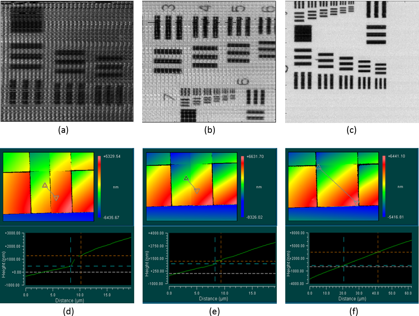
Reconstructed images of 1951 USAF resolution targets and corresponding characterization images from a Zygo white light interferometer of three mapping mirrors during optimization. (a) Reconstructed images from the mapping mirror printed with 1 μm slicing distance and 0.2 μm hatching distance. (b) Reconstructed images from the mapping mirror printed with a base added in the GrayscribeX software. (c) Reconstructed images from the mapping mirror printed with an extra base added to the design. (d) 50× characterization image of the mapping mirror in (a). (e) Characterization image of the mapping mirror in (b). (f) Characterization image of the mapping mirror in (c).
The printing FOV was initially set to be 468 μm, which was the size of six pixels. All imaging systems will have optical aberrations, and field-dependent aberrations (field curvature and astigmatism) will be significantly larger at the edge of the FOV. Therefore, the printing FOV was adjusted to 390 μm, which is 1 pixel (78 μm) smaller than the previous one. The printing result is shown in Fig. 6(b). The defect in the stitching area improved to 262 nm. The mapping mirror was also implemented in the prototype system. The reconstructed image of the USAF resolution target [Fig. 6(e)] shows improved image quality and dynamic range. The dark stripes become thinner but still show up on the final images. Note that the printer would find the interface between the fused silica slide and IP-S resin when moving to a new printing FOV. Therefore, if the slide with resin on top has a small overall tilt, the printer will have various starting positions in the dimension for each printing FOV.
The overall tilt needs to be measured to add compensation. Before the printing job, the printer focused on nine different points (3 × 3) and recorded the positions of all the points. The overall tilt was affected by the optomechanics of the slide mounting and the thickness tolerance of slide fabrication, so the tilt angles were different for each printing. For this mapping mirror printing job, the tilt angles in horizontal and vertical direction are 0.07° and 0.04°, respectively. A compensation file was added based on these angles, while a dispenser was required to constantly inject IP-S resin to keep the objective immersed. The dispenser injected 0.1 mL resin at the beginning of the job and 0.005 mL resin at each printing FOV. A portion of the mapping mirror with tilt compensation was imaged by a SEM (Merlin, FE-SEM, Zeiss, Germany) as shown in Fig. 4(c). Even though the printing FOV is five mirror size, no visible stitching defects are observed on the image. The magnified 2 × 2 mirror images, Fig. 4(d), further demonstrate the fabrication quality of surface roughness and form. The reconstructed image from the optimized mapping mirror is shown in Fig. 6(c). There are no strong stripes along any direction, leading to a better resolution of the finest resolution bar. Moreover, the elimination of saturated points due to the defects has led to a notable enhancement in the dynamic range. This advancement is beneficial to fluorescent imaging.
B. Spectral Imaging
The IMS prototype was also used to image bovine pulmonary artery endothelial (BPAE) cells (Thermo Fisher Scientific Inc., MA) stained with three fluorescent dyes: DAPI, Alexa Fluor 488 phalloidin, and Mito Tracker Red CMXRos. The prototype IMS had 412 × 480 × 44 datacubes. Pseudo-color images of 25 spectral channels corresponding to the three fluorescent dyes were obtained with an integration time of 80 ms, as shown in Fig. 7. The blue channels did not show strong DAPI signals due to the relatively low quantum efficiency of the camera in the blue range and the lower fluorescent signal level of the DAPI fluorescent dyes. However, F-actin and mitochondria of BPAE cells could be observed. These spectral images demonstrate that 2PP 3D printed mapping mirrors can achieve the same functionality as diamond-cut mapping mirrors. In addition, the image quality improved compared to the latest IMS images [20]. To further demonstrate that mapping mirror quality can enable expected spectral resolution as an average of 5 nm, two narrowband filters with center wavelengths of 515 and 589 nm were imaged. As shown in Fig. 8, the maximum signals from all spectral channels were plotted and fitted using the Gaussian function to determine the center of the spectral responses. The center position from the Gaussian fitting for the 515 nm filter imaging [Fig. 8(a)] was 517.2 nm with a deviation within the spectral resolution, while for the 589 nm filter imaging, the fitted center wavelength was 589.7 nm [Fig. 8(a)], which was close to the 589 nm.
Fig. 7.
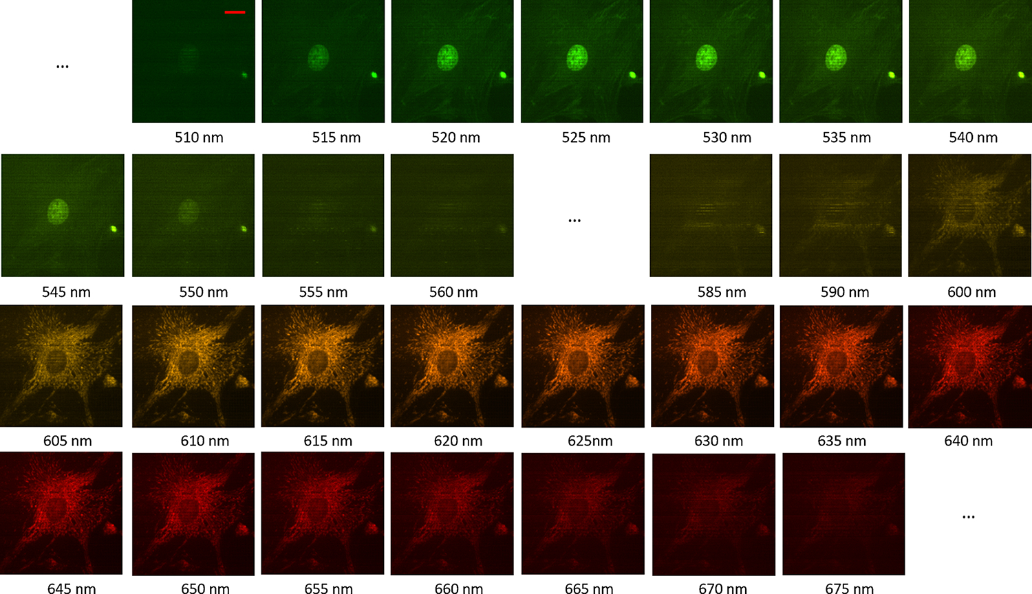
Pseudo-color images of 25 selected channels for the BPAE cell imaging. In the 510 nm images, the represented distance is 15 μm as indicated by the scale bar.
Fig. 8.
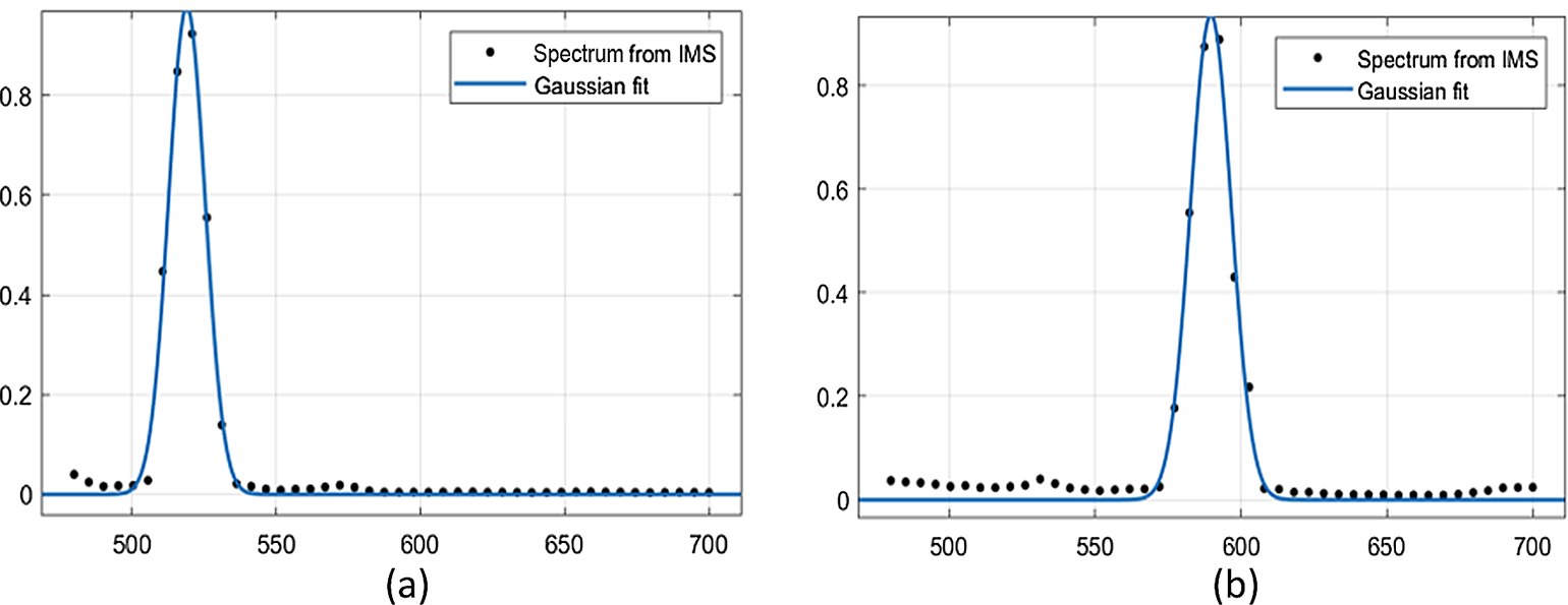
Gaussian fitting of two narrowband filters with center wavelengths at 515 and 589 nm. (a) Gaussian fitting for 515 nm narrowband filter. (b) Gaussian fitting for 589 nm narrow band filter.
The system design and performance allow the same level of spatial resolution as other systems such as hyperspectral confocal systems or filter scanning systems. Note that in the past, we evaluated IMS for general operational parameters such as optical sectioning, imaging speed/SNR, and photo-bleaching rates [8]. The spectral images are used to demonstrate that 2PP 3D printed mapping mirrors have the same functionality as diamond-cut mapping mirrors in the IMS system. The structure quality and reflection rate are further highlighted.
7. CONCLUSIONS AND FUTURE DIRECTIONS
A new fabrication method based on 2PP is demonstrated to successfully fabricate high-precision optical mapping mirrors. The minimum angle increment for 78 μm facets in ideal conditions is 1.0%. Although our obtained tilt values fell outside the range attributed to the shrinkage of facets, the results still represent a significant improvement over prior mapping mirror implementations and fall within the 6% tolerance allowed by the IMS system. Acceptable surface roughness is 10–15 nm, and the average surface roughness was found to be within the expected range. Furthermore, the expected less than 1% facet width change was achieved because of the fine hatching and slicing distance, which keeps dynamic loss below 0.5%. In general, the resulting 3D printed mapping mirrors exhibit superior surface quality and address the limitations of existing IMS systems, such as reduced dynamic range, prolonged production time, and complex calibration procedures. This new fabrication method considerably reduces the challenges involved in creating an IMS system and has the potential to expand the range of applications for IMS technology.
There remains scope for further advancements in the fabrication of mapping mirrors. To facilitate future printings, a datasheet containing fabrication parameters based on tilt angles will be useful. Furthermore, a large-scale 10× objective is available, which can significantly reduce the fabrication time from 70–80 h to less than 2–5 h. We do not expect, however, direct mass production of mapping mirrors using 2PP, even with the 10× objective. Instead of printing the mapping mirrors themselves, QuantumX produced parts can be nickel plated and post-processed to burn-out polymer. This will allow producing molds and enable higher volume fabrication. Such an approach will also reduce the fabrication cost of mapping components to similar levels of molded optics components. The printing parameters and procedures reported in this work can be applied to any microstructure with sharp edges. For example, reflective and transmission gratings can be simplified cases of mapping mirrors, as they involve only 1D tilt.
Acknowledgment.
We acknowledge all the members in Tkaczyk lab for the helpful discussions and assistance.
Funding.
National Institutes of Health (R01DK115972).
Footnotes
Disclosures. Dr. Tomasz Tkaczyk has financial interests in Attoris LLC. The authors declare no conflicts of interest.
Data availability.
Data underlying the results presented in this paper are not publicly available at this time but may be obtained from the authors upon reasonable request.
REFERENCES
- 1.Hege EK, O’Connell D, Johnson W, Basty S, and Dereniak EL, “Hyperspectral imaging for astronomy and space surveillance,” Proc. SPIE 5159, 380–391 (2004). [Google Scholar]
- 2.Rafert B, Sellar RG, Holbert E, Blatt JH, Tyler DW, Durham SE, and Newby HD, “Hyperspectral imaging Fourier transform spectrometers for astronomical and remote sensing observations,” Proc. SPIE 2198, 338–349 (1994). [Google Scholar]
- 3.Gowen AA, O’Donnell CP, Cullen PJ, Downey G, and Frias JM, “Hyperspectral imaging–an emerging process analytical tool for food quality and safety control,” Trends Food Sci. Technol. 18, 590–598 (2007). [Google Scholar]
- 4.Adão T, Hruška J, Pádua L, Bessa J, Peres E, Morais R, and Sousa JJ, “Hyperspectral imaging: a review on UAV-based sensors, data processing and applications for agriculture and forestry,” Remote Sens. 9, 1110 (2017). [Google Scholar]
- 5.Park B and Lu R, Hyperspectral Imaging Technology in Food and Agriculture (Springer, 2015). [Google Scholar]
- 6.Lu B, Dao PD, Liu J, He Y, and Shang J, “Recent advances of hyperspectral imaging technology and applications in agriculture,” Remote Sens. 12, 2659 (2020). [Google Scholar]
- 7.Lu G and Fei B, “Medical hyperspectral imaging: a review,” J. Biomed. Opt. 19, 010901 (2014). [DOI] [PMC free article] [PubMed] [Google Scholar]
- 8.Gao L, Kester RT, Hagen N, and Tkaczyk TS, “Snapshot image mapping spectrometer (IMS) with high sampling density for hyperspectral microscopy,” Opt. Express 18, 14330–14344 (2010). [DOI] [PMC free article] [PubMed] [Google Scholar]
- 9.Wolfe WL, Introduction to Imaging Spectrometers (SPIE, 1997), Vol. 25. [Google Scholar]
- 10.Wang SC and Flagan RC, “Scanning electrical mobility spectrometer,” Aerosol Sci. Technol. 13, 230–240 (1990). [Google Scholar]
- 11.Sun M and Zigman S, “An improved spectrophotometric assay for superoxide dismutase based on epinephrine autoxidation,” Anal. Biochem. 90, 81–89 (1978). [DOI] [PubMed] [Google Scholar]
- 12.Kerr J, “New methodology for deriving total ozone and other atmospheric variables from brewer spectrophotometer direct sun spectra,” J. Geophys. Res. Atmos. 107, ACH-22 (2002). [Google Scholar]
- 13.Gao L and Wang LV, “A review of snapshot multidimensional optical imaging: measuring photon tags in parallel,” Phys. Rep. 616, 1–37 (2016). [DOI] [PMC free article] [PubMed] [Google Scholar]
- 14.Wang Y, Pawlowski ME, and Tkaczyk TS, “High spatial sampling light-guide snapshot spectrometer,” Opt. Eng. 56, 081803 (2017). [DOI] [PMC free article] [PubMed] [Google Scholar]
- 15.Wang Y, Pawlowski ME, Cheng S, Dwight JG, Stoian RI, Lu J, Alexander D, and Tkaczyk TS, “Light-guide snapshot imaging spectrometer for remote sensing applications,” Opt. Express 27, 15701–15725 (2019). [DOI] [PubMed] [Google Scholar]
- 16.Lu J, Ng XW, Piston D, and Tkaczyk TS, “Snapshot image mapping spectrometer with 3d printed multifaceted mapping mirror for biomedical applications,” Proc. SPIE 12216, 63–68 (2022). [Google Scholar]
- 17.Hagen NA and Kudenov MW, “Review of snapshot spectral imaging technologies,” Opt. Eng. 52, 090901 (2013). [Google Scholar]
- 18.Hagen N and Dereniak EL, “Analysis of computed tomographic imaging spectrometers. i. spatial and spectral resolution,” Appl. Opt. 47, F85–F95 (2008). [DOI] [PubMed] [Google Scholar]
- 19.Dwight JG, Weng CY, Coffee RE, Pawlowski ME, and Tkaczyk TS, “Hyperspectral image mapping spectrometry for retinal oximetry measurements in four diseased eyes,” Int. Ophthalmol. Clin. 56, 25 (2016). [DOI] [PMC free article] [PubMed] [Google Scholar]
- 20.Pawlowski ME, Dwight JG, Nguyen T-U, and Tkaczyk TS, “High performance image mapping spectrometer (IMS) for snapshot hyperspectral imaging applications,” Opt. Express 27, 1597–1612 (2019). [DOI] [PMC free article] [PubMed] [Google Scholar]
- 21.Kester RT, Gao L, and Tkaczyk TS, “Development of image mappers for hyperspectral biomedical imaging applications,” Appl. Opt. 49, 1886–1899 (2010). [DOI] [PMC free article] [PubMed] [Google Scholar]
- 22.Gao LS and Tkaczyk TS, “Correction of vignetting and distortion errors induced by two-axis light beam steering,” Opt. Eng. 51, 043203 (2012). [DOI] [PMC free article] [PubMed] [Google Scholar]
- 23.Dubbeldam CM, Robertson DJ, and Preuss W, “Freeform diamond machining of complex monolithic metal optics for integral field systems,” Proc. SPIE 5494, 163–175 (2004). [Google Scholar]
- 24.Vives S, Prieto E, Salaun Y, and Godefroy P, “New technological developments in integral field spectroscopy,” Proc. SPIE 7018, 959–968 (2008). [Google Scholar]
- 25.Gonzalez-Hernandez D, Varapnickas S, Bertoncini A, Liberale C, and Malinauskas M, “Micro-optics 3D printed via multi-photon laser lithography,” Adv. Opt. Mater. 11, 2201701 (2023). [Google Scholar]
- 26.Berglund G, Wisniowiecki A, Gawedzinski J, Applegate B, and Tkaczyk TS, “Additive manufacturing for the development of optical/photonic systems and components,” Optica 9, 623–638 (2022). [Google Scholar]
- 27.Fatkullin N, Ikehara T, Jinnai H, Kawata S, Kimmich R, Nishi T, Nishikawa Y, Sun H-B, Sun H-B, and Kawata S, Two-Photon Photopolymerization and 3D Lithographic Microfabrication (Springer, 2004). [Google Scholar]
- 28.Gan Z, Cao Y, Evans RA, and Gu M, “Three-dimensional deep sub-diffraction optical beam lithography with 9 nm feature size,” Nat. Commun. 4, 2061 (2013). [DOI] [PubMed] [Google Scholar]
- 29.Jonušauskas L, Gailevičius D, Rekštytė S, Baldacchini T, Juodkazis S, and Malinauskas M, “Mesoscale laser 3d printing,” Opt. Express 27, 15205–15221 (2019). [DOI] [PubMed] [Google Scholar]
- 30.Gissibl T, Thiele S, Herkommer A, and Giessen H, “Sub-micrometre accurate free-form optics by three-dimensional printing on single-mode fibres,” Nat. Commun. 7, 1–9 (2016). [DOI] [PMC free article] [PubMed] [Google Scholar]
- 31.Bertoncini A, Laptenok SP, Genchi L, Rajamanickam VP, and Liberale C, “3D-printed high-NA catadioptric thin lens for suppression of XPM background in stimulated Raman scattering microscopy,” J. Biophoton. 14, e202000219 (2021). [Google Scholar]
- 32.Gissibl T, Thiele S, Herkommer A, and Giessen H, “Two-photon direct laser writing of ultracompact multi-lens objectives,” Nat. Photonics 10, 554–560 (2016). [Google Scholar]
- 33.Schäffner D, Preuschoff T, Ristok S, Brozio L, Schlosser M, Giessen H, and Birkl G, “Arrays of individually controllable optical tweezers based on 3D-printed microlens arrays,” Opt. Express 28, 8640–8645 (2020). [DOI] [PubMed] [Google Scholar]
- 34.Purtov J, Rogin P, Verch A, Johansen VE, and Hensel R, “Nanopillar diffraction gratings by two-photon lithography,” Nanomaterials 9, 1495 (2019). [DOI] [PMC free article] [PubMed] [Google Scholar]
- 35.Mu J, Liu Z, Li J, Hao T, Wang Y, Sun S, Li Z-Y, Li J, Li W, and Gu C, “Direct laser writing of pyramidal plasmonic structures with apertures and asymmetric gratings towards efficient subwavelength light focusing,” Opt. Express 23, 22564–22571 (2015). [DOI] [PubMed] [Google Scholar]
- 36.Xiao TP, Cifci OS, Bhargava S, Chen H, Gissibl T, Zhou W, Giessen H, Toussaint KC Jr., Yablonovitch E, and Braun PV, “Diffractive spectral-splitting optical element designed by adjoint-based electromagnetic optimization and fabricated by femtosecond 3D direct laser writing,” ACS Photon. 3, 886–894 (2016). [Google Scholar]
- 37.Aderneuer T, Fernández O, and Ferrini R, “Two-photon grayscale lithography for free-form micro-optical arrays,” Opt. Express 29, 39511–39520 (2021). [DOI] [PubMed] [Google Scholar]
- 38.Dehaeck S, Scheid B, and Lambert P, “Adaptive stitching for meso-scale printing with two-photon lithography,” Addit. Manuf. 21, 589–597 (2018). [Google Scholar]
- 39.Rodrguez S, “Redefining microfabrication of high-precision optics: how two-photon grayscale lithography improves quality and throughput of printing microparts,” PhotonicsViews 17, 36–39 (2020). [Google Scholar]
- 40.Nanoscribe, “Quantum X,” https://www.nanoscribe.com/en/products/quantum-x/.
Associated Data
This section collects any data citations, data availability statements, or supplementary materials included in this article.
Data Availability Statement
Data underlying the results presented in this paper are not publicly available at this time but may be obtained from the authors upon reasonable request.


