Abstract
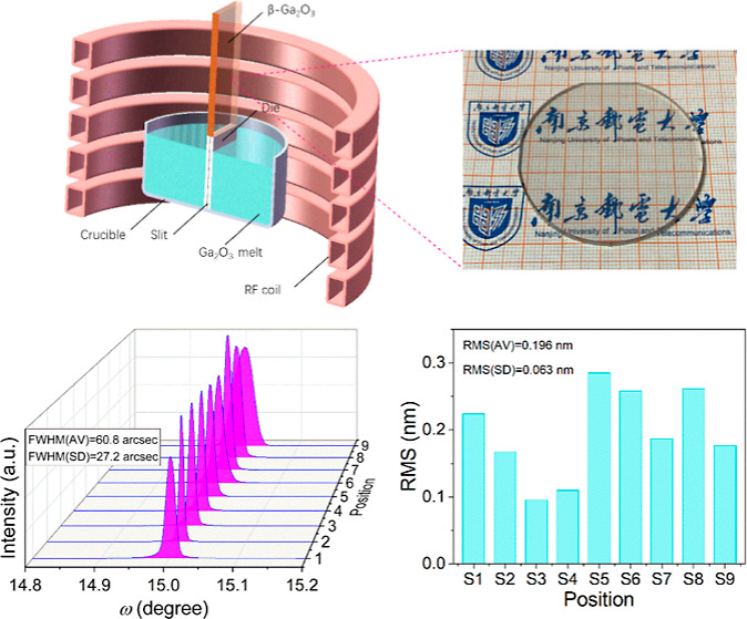
2 in. bulk β-Ga2O3 single crystals are successfully grown by the edge-defined film-fed growth method with a homemade furnace system. By considering the significance of wafer quality in future mass manufacture, a nine-point characterization method is developed to evaluate the full-scale quality of the processed 2 in. (100)-orientated β-Ga2O3 single-crystal wafers. Crystalline and structural characteristics were evaluated using X-ray diffraction and Raman spectroscopy, revealing decent crystalline quality with a mean full width at half-maximum value of 60.8 arcsec and homogeneous bonding structures. The statistical root-mean-square surface roughness, determined from nine scanning areas, was found to be only 0.196 nm, indicating superior surface quality. Linear optical properties and defect levels were further investigated using UV–visible spectrophotometry and photoluminescence spectroscopy. The high wafer-scale quality of the processed β-Ga2O3 wafers meets the requirements for homoepitaxial growth substrates in electronic and photonic devices with vertical configurations.
Introduction
As a new emerging ultrawide band gap semiconductor, gallium oxide (Ga2O3) possesses a large band gap of 4.9 eV, a high breakdown field of 8 MV/cm, and a desirable Baliga’s figure of merit of 3214. Additionally, it exhibits strong bonding structures with Ga- and O-displacement energies of 25 and 28 eV, respectively.1,2 These excellent material characteristics enable Ga2O3 to find extensive applications in electronic and optoelectronic devices, even comparable with GaN and SiC.3,4 In recent years, numerous successful device demonstrations of Ga2O3, such as deep-ultraviolet photodetectors,5−7 resistive random access memories,8,9 gas sensors,10 light-emitting diodes,11 photocatalysts,12 Schottky diodes, heterojunction diodes, and metal oxide semiconductor field effect transistors for power devices,13−15 have been explored and investigated experimentally. In all examples, the performance of these devices is highly dependent on the material merit of Ga2O3. Especially for power electronics, β-Ga2O3 single crystals with appropriate size and high wafer-scale quality are of essence to fabricate high-performance devices.
Up to now, many common techniques, including Verneuil,16 Czochralski (CZ),17 floating-zone (FZ),18 edge-defined film-fed growth (EFG),19 and horizontal or vertical Bridgman methods,20 have been developed to grow bulk β-Ga2O3 single crystals. Among them, the EFG technique shows the most promising commercial potential due to its availability of large-diameter β-Ga2O3 wafers with an acceptable quality. The successful growth of 2 in. β-Ga2O3 bulk crystal via the EFG method was first reported by Shimamura et al., although their obtained crystal was heavily cracked.21 Aida et al. realized 50 mm size of large-diameter β-Ga2O3 crystals without any polycrystalline inclusions by the EFG method.19 Research team from Tamura and Novel Crystal Technology scaled the β-Ga2O3 wafer diameter up to 4 in. and achieved a narrow full width at half-maximum (fwhm) of 17 arcsec in the 2 in. (−201) substrate.22 Si-doped 2 in. β-Ga2O3 prepared by Zhang et al. demonstrated an fwhm of 19.06 arcsec and a surface roughness of 0.299 nm.23 Mu et al. from Shandong University grew 1 in. β-Ga2O3 crystals using an optimized EFG method under an atmosphere of Ar plus 50% CO2.24 Subsequently, they designed and grew cylindrical Sn-doped β-Ga2O3 crystals using an innovative EFG furnace equipped with a cylindrical iridium die, which exhibited decent crystalline quality with an fwhm of 59.4 arcsec.25 Despite the significant breakthroughs achieved in obtaining large-diameter β-Ga2O3 single crystals, the quality of bulk crystals, including the aforementioned examples, is typically characterized and represented by single-point performance testing. However, this approach may not fully reflect the crystal quality at the wafer-scale size.
In view of the crucial role of wafer quality in future mass device manufacture, a nine-point characterization method is developed and adopted here to assess the full-scale wafer quality of 2 in. β-Ga2O3 single crystals. The bulk β-Ga2O3 crystals are grown by a homemade EFG furnace in a mixture atmosphere of 98% Ar and 2% O2. Consequently, these crystals undergo a sequence of procedures involving cutting, grinding, and polishing to fashion them into 2 in. thin wafers with a thickness measuring 650 μm. The crystalline and structural integrity, surface topography, optical characteristics, and defect levels of the β-Ga2O3 wafers are meticulously scrutinized employing techniques such as high-resolution X-ray diffraction, Raman spectroscopy, atomic force microscopy, UV–visible spectrophotometry, and photoluminescence (PL) spectroscopy, employing a rigorous nine-point evaluation scheme. The experimental findings demonstrate that the 2 in. β-Ga2O3 substrates cultivated and processed in our study exhibit exceptional quality at the wafer scale.
Experimental Section
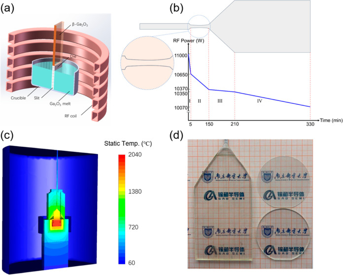
Bulk β-Ga2O3 single crystals grown in an iridium crucible with an iridium die by EFG furnace are sectionally shown in Figure 1a. 5N-grade Ga2O3 powders were filled in the iridium crucible to use as the raw materials. The chamber pressure was around 105 kPa accompanied by a mixture atmosphere of 98% Ar and 2% O2. A radio frequency induction coil was employed as a heating source and regulated by a specific temperature rising program. As the heating temperature reached up to a melting point of ∼1800 °C, the Ga2O3 melt would transport from the crucible to the die surface through a slit by the capillary effect. Then, a strip-type β-Ga2O3 seed right above the crucible was programed moving down to contact Ga2O3 melt over the die surface. The typical β-Ga2O3 EFG process combined with RF power profiles is illustrated in Figure 1b. There are four classic growth stages including (I) seeding process, (II) necking process, (III) spreading process, and (IV) steady-growth process. The static temperature distribution of the EFG furnace system during the steady-growth process was simulated numerically with ANSYS software in Figure 1c. The growth direction was along [010], and the principal surface was the (100) plane. The growth temperature was tracked by an infrared thermometer all of the time. The crystal weight was continuously monitored with an accurate weighing system through a seed rod. A high-definition camera equipped with a polarizer was utilized to observe the die surface. Therefore, the pulling speed could be adjusted by observing the real-time crystal weight and surface morphology. The conventional pulling speed in our experiment was set in the range of 10–30 mm/h.
Figure 1.
(a) Schematic diagram of the furnace for the EFG process; (b) growth stages and RF power profiles; (c) static temperature distribution of the furnace system during the steady-growth process, and (d) pictures of an initial bulk crystal and two processed 2 in. wafers (Photograph courtesy of Ganrong Feng and Shan Li, Copyright 2024).
The pristine bulk Ga2O3 single crystals were accordingly processed by wire cutting, diamond slurry grinding, and chemical mechanical polishing to fabricate the standard 2 in. wafers, as illustrated in Figure 1d. To obtain a full-scale evaluation of a 2 in. β-Ga2O3 wafer, nine points were uniformly selected on the wafer as measuring regions. The crystalline quality was characterized via high resolution X-ray diffraction (XRD) (Bruker D8 ADVANCE). The Raman and PL spectra were recorded by a Raman spectrometer (Renishaw inVia) and LED measurement system (Etamax PLATO), respectively. The surface morphologies were measured with atomic force microscopy (AFM, Bruker Dimension Fast-Scan). The optical absorption spectra and the corresponding bandgaps (Eg) were obtained by UV–visible spectrophotometry (Macy UV1900).
Results and Discussion
The typical dimensions of the as-grown β-Ga2O3 bulk crystals are 80 mm length, 55 mm width, and 5 mm thickness. Notably, the width and thickness of the crystals are entirely contingent upon the design specifications of the iridium die top, as illustrated in Figure 1a. In our investigation, the die top shape is rectangular, measuring 5 × 55 mm2. The crystal length relies on the filling amount of Ga2O3 powders in the crucible and the growth time of exhausting these raw powders. Figure 1b illustrates the RF power alongside the process time, offering concrete process parameters crucial for both scientific research and industrial production. The static temperature distribution, as depicted in Figure 1c, exhibits a stable temperature gradient along the axial direction, facilitating ample Gibbs free energy for the growth of the β-Ga2O3 bulk crystals.
In Figure 1d, the initial bulk crystal and two processed 2 in. wafers are presented. Through meticulous cutting and polishing processes, the bulk thickness of the 2 in. β-Ga2O3 wafer is typically reduced to 650 μm. The principal plane, denoted as (100), and the side plane formed from the die shoulder, denoted as (001), are discernible. The cross-section along the growth orientation corresponds to the (010) plane. These double-side-polished wafers exhibit no apparent defects such as twin crystals or cracks. These unintentionally doped β-Ga2O3 single crystals are manifested as colorless with high transparency.
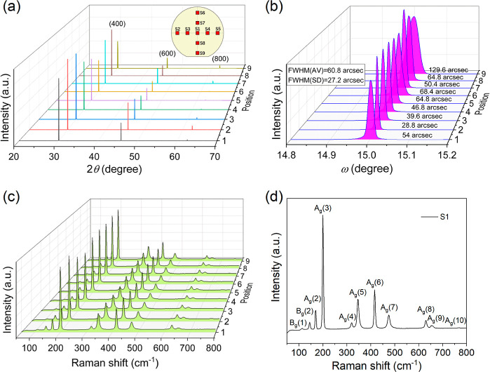
Theta-2theta XRD patterns of the 2 in. β-Ga2O3 wafer are illustrated in Figure 2a. The inset displays the distribution of nine mensurated points across the wafer, labeled as S1–S9. Three distinct diffraction peaks are discernible in all curves, situated at 2theta positions of 30.02, 45.74, and 62.46°, aligning with the (400), (600), and (800) planes of the β-phase monoclinic crystal structure.26,27Figure 2b presents X-ray rocking curves evaluated on the (400) planes. All nine rocking curves depict pronounced and well-defined diffraction peaks with fwhm values ranging from 28.8 to 129.6 arcsec. The average fwhm value (AV) is calculated to be 60.8 arcsec, with a corresponding standard deviation (SD) of 27.2 arcsec. These outcomes underscore the high crystalline quality of our 2 in. wafer, surpassing even some FZ- and EFG-grown β-Ga2O3 crystals.18,19
Figure 2.
(a) Nine-point theta-2theta XRD patterns (the inset is the distribution map of nine mensurated points) and (b) nine-point rocking curves; (c) nine-point Raman spectra, and (d) S1 Raman spectrum with marked peaks.
Figure 2c shows the unpolarized room-temperature Raman spectra of the 2 in. β-Ga2O3 wafer. It is obvious that Raman spectra recorded at nine distinct positions exhibit identical phonon modes and similar peak intensities. This remarkable consistency underscores not only the excellent crystalline quality but also the homogeneity of the wafer-scale material. Chosen S1 as the representative in Figure 2d, Raman peaks could be detected at 113.6, 145.0, 170.4, 199.6, 321.0, 345.9, 416.1, 474.5, 630.5, 654.3, and 767.1 cm–1, matching well to the experimental and computational values.23,28 These Raman peaks can be assigned to Bg(1), Bg(2), Ag(2), Ag(3), Ag(4), Ag(5), Ag(6), Ag(7), Ag(8), Ag(9), and Ag(10) modes, as labeled in Figure 2d. The low-frequency phonon modes [Bg(1), Bg(2), Ag(2), Ag(3)] are related to the liberation and translation of GaIO4 chains, the midfrequency phonon modes [Ag(4), Ag(5), Ag(6), Ag(7)] are caused by the deformation of GaIO4 and GaIIO6, and the high-frequency phonon modes are ascribed to the stretching and bending of GaIO4.23,28,29
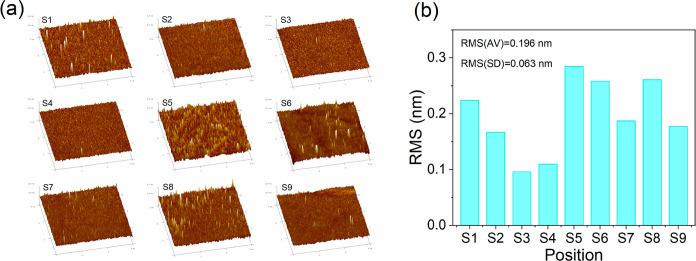
The wafer surface quality is characterized by nine-point 3D AFM morphologies, as exhibited in Figure 3a. Each point surface morphology is recorded within a scanning area of 3 × 3 μm2. With the same color scale bar (from −2 to 2 nm), some spiculate bulges and linear pits can be found in 3D topography, which are crucial for the root-mean-square (RMS) surface roughness. The recorded spiculate bulges are mainly caused by unremoved nanosized abrasive SiO2 powder. The linear pits are polishing scratches and mechanical damages.30 Even counting in the unintentional surface damages resulting from the chemical mechanic polishing, all nine-point RMS values are within 0.3 nm, as summarized in Figure 3b. The AV RMS is just 0.196 nm (the nine-point SD is only 0.063 nm), better than the reported values of 0.23 and 0.26 nm,31 demonstrating a high surface quality of our 2 in. β-Ga2O3 wafer.
Figure 3.
(a) Nine-point AFM images and the (b) corresponding RMS values.
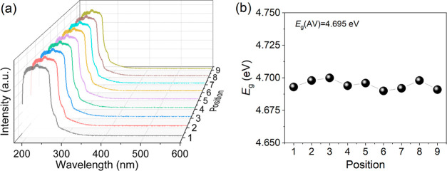
The optical absorption property of the β-Ga2O3 wafer is plotted in Figure 4a at a wavelength range of 190–600 nm. Nine-point measurements across the whole 2 in. wafer perform highly similar absorption features. All spectral curves show the same absorption shoulder at a wavelength of 270–280 nm, which has also been observed previously in Ga2O3.23,32 Such an absorption shoulder is not affected by the doping contents.23,32 Therefore, this particular absorption shoulder should be caused by an intrinsic defect. In consideration of the deep energy level of the absorption shoulder, it is most likely resulted by oxygen vacancy with one or two trapped electrons just as reported in the other metal oxides.33−36 However, Harwig et al. and Wang et al. ascribe it to the presence of a self-trapped hole level in β-Ga2O3, which is about 0.25 eV above the valence band maximum.32,37 Although some literature has attempted to explain the absorption shoulder, there is still no final conclusion and more in-depth and direct studies are needed. In view of the fact that β-Ga2O3 possesses a direct optical band gap, the Eg values of nine points are estimated according to Tauc’s principle as previously reported.38−41 As plotted in Figure 4b, the direct Eg values extracted from nine-point absorption spectra show tiny difference, with an average value of 4.695 eV. Such identical absorption curves and stable band gap values in different regions of 2 in. wafer indicate homogeneous linear optical properties of the grown β-Ga2O3 bulk crystals.
Figure 4.
(a) Nine-point absorption curves and the (b) corresponding band gap values.
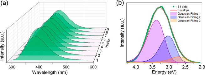
To qualitatively understand the defect levels of β-Ga2O3, PL characteristics are performed on a 2 in. wafer using a 266 nm HeCd laser excitation source according to the nine-point test method. As shown in Figure 5a, the intensities of PL transitions acquired from different regions display a slight fluctuation. However, each region shows a similarly asymmetric and consistently broad PL band spanning from 300 to 600 nm, implying that the 2 in. wafer performs uniform defect levels in large-area. An individual spectrum of S1 is chosen as a representative to take a deep investigation with Gaussian distribution to fit the experimental data in the energy scale, as presented in Figure 5b.42 The S1 PL spectrum can be deconvolved into three dominant peaks at energy levels of 3.38 eV (367 nm), 3.02 eV (411 nm), and 2.70 eV (460 nm).43,44 Three luminescence peaks are attributed to radiative recombination of electrons from the conduction band edge with holes in the acceptor bands (such as the self-trapped holes between two OII-s sites, the gallium–oxygen vacancy pairs, and the gallium vacancies at tetrahedral sites), which give rise to ultraviolet-blue emissions as reported.43,45
Figure 5.
(a) Nine-point PL spectra and (b) S1 PL spectrum with Gaussian peak fitting.
Conclusions
In summary, a 2 in. diameter bulk β-Ga2O3 single crystal has been successfully cultivated via the EFG method employing a custom-built furnace system. Following cutting, grinding, and polishing procedures, the resulting β-Ga2O3 single-crystal substrates demonstrate high-quality characteristics at the wafer scale, assessed using a comprehensive nine-point evaluation approach. Notably, the average fwhm, RMS, and Eg for the double-side polished 2 in. β-Ga2O3 wafer are determined to be 60.8 arcsec, 0.196 nm, and 4.695 eV, respectively, indicating commendable crystalline quality, smooth surface morphology, and desirable linear optical properties. Furthermore, structural quality and defect characteristics are meticulously scrutinized through Raman and PL measurements, reinforcing the assertion that the wafer quality exhibits not only excellence but also uniformity across the entire surface. The experimentally obtained outstanding material properties position our 2 in. β-Ga2O3 single-crystal wafers as highly suitable substrates for deployment in homoepitaxial growth processes and the manufacturing of electronic and photonic devices featuring vertical configurations.
Acknowledgments
This work was funded by the National Key Research and Development Program of China (grant no. 2022YFB3605404), the Joint Funds of the National Natural Science Foundation of China (grant no. U23A20349), the National Natural Science Foundation of China (grant no. 62305171), the Jiangsu Provincial Team of Innovation and Entrepreneurship (grant no. CZ118SC23058), the Natural Science Foundation of Jiangsu Province (grant no. BK20230361), the Natural Science Foundation of Jiangsu Higher Education Institutions (grant no. 23KJB510017), and the Natural Science Research Start-up Foundation of Recruiting Talents of NJUPT (grant nos. XK1180922062 and XK1060921002). Ga2O3 single crystals used in this research project are from Beijing GAO Semiconductor Co. Ltd. (S.L., sli@gaosemi.cn).
The authors declare no competing financial interest.
References
- Pearton S. J.; Yang J.; Cary P. H.; Ren F.; Kim J.; Tadjer M. J.; Mastro M. A. A Review of Ga2O3 Materials, Processing, and Devices. Appl. Phys. Rev. 2018, 5 (1), 011301. 10.1063/1.5006941. [DOI] [Google Scholar]
- Farzana E.; Chaiken M. F.; Blue T. E.; Arehart A. R.; Ringel S. A. Impact of Deep Level Defects Induced by High Energy Neutron radiation in β-Ga2O3. APL Mater. 2019, 7 (2), 022502. 10.1063/1.5054606. [DOI] [Google Scholar]
- Li S.; Liu Z.; Zhang M.; Yang L.; Guo Y.; Tang W. High-performance self-powered GaN/PEDOT:PSS hybrid heterojunction UV photodetector for optical communication. Sci. China: Technol. Sci. 2023, 67, 608–615. 10.1007/s11431-023-2501-5. [DOI] [Google Scholar]
- Li S.; Yang L.; Liu Z.; Zhang M.; Guo Y.; Tang W. Hybrid PEDOT:PSS/SiC heterojunction UV photodetector with superior self-powered responsivity over A/W level. Appl. Phys. Lett. 2023, 122 (19), 191102. 10.1063/5.0150344. [DOI] [Google Scholar]
- Wang X.; Ding K.; Huang L.; Li X.; Ye L.; Luo J.; Jiang J.; Li H.; Xiong Y.; Ye L.; Pang D.; Tang Y.; Li W.; Zhang H.; Kong C. Enhancing the performance of Self-Powered Deep-Ultraviolet photoelectrochemical photodetectors by constructing α-Ga2O3@a-Al2O3 Core-Shell nanorod arrays for Solar-Blind imaging. Appl. Surf. Sci. 2024, 648, 159022. 10.1016/j.apsusc.2023.159022. [DOI] [Google Scholar]
- Li S.; Yue J.; Ji X.; Lu C.; Yan Z.; Li P.; Guo D.; Wu Z.; Tang W. Oxygen Vacancies Modulating the Photodetector Performances in ε-Ga2O3 Thin Films. J. Mater. Chem. C 2021, 9 (16), 5437–5444. 10.1039/D1TC00616A. [DOI] [Google Scholar]
- Li S.; Yan Z.; Liu Z.; Chen J.; Zhi Y.; Guo D.; Li P.; Wu Z.; Tang W. A Self-Powered Solar-Blind Photodetector with Large VOC Enhancing Performance Based on the PEDOT:PSS/Ga2O3 Organic-Inorganic Hybrid Heterojunction. J. Mater. Chem. C 2020, 8 (4), 1292–1300. 10.1039/C9TC06011A. [DOI] [Google Scholar]
- Baunthiyal A.; Krisponeit J.-O.; Schowalter M.; Mehrtens T.; Karg A.; Rosenauer A.; Eickhoff M.; Falta J. Growth and characterization of sputter-deposited Ga2O3-based memristive devices. Appl. Phys. Lett. 2023, 123 (21), 213504. 10.1063/5.0170354. [DOI] [Google Scholar]
- Li W.; Wan J.; Tu Z.; Li H.; Wu H.; Liu C. Optimizing endurance performance of Ga2O3 random resistive access memories by altering oxygen vacancy content. Ceram. Int. 2022, 48 (3), 3185–3191. 10.1016/j.ceramint.2021.10.091. [DOI] [Google Scholar]
- Zhai H.; Wu Z.; Fang Z. Recent progress of Ga2O3-based gas sensors. Ceram. Int. 2022, 48 (17), 24213–24233. 10.1016/j.ceramint.2022.06.066. [DOI] [Google Scholar]
- Chen Z.; Saito K.; Tanaka T.; Guo Q. Near-infrared light-emitting diodes based on Tm-doped Ga2O3. J. Lumin. 2022, 245, 118773. 10.1016/j.jlumin.2022.118773. [DOI] [Google Scholar]
- Qiu H.; Yamamoto A.; Yoshida H. Gallium Oxide Assisting Ag-Loaded Calcium Titanate Photocatalyst for Carbon Dioxide Reduction with Water. ACS Catal. 2023, 13 (6), 3618–3626. 10.1021/acscatal.2c06038. [DOI] [Google Scholar]
- Wong M. H. A landscape of β-Ga2O3 Schottky power diodes. J. Semicond. 2023, 44 (9), 091605. 10.1088/1674-4926/44/9/091605. [DOI] [Google Scholar]
- Zhou F.; Gong H.; Xiao M.; Ma Y.; Wang Z.; Yu X.; Li L.; Fu L.; Tan H. H.; Yang Y.; Ren F.-F.; Gu S.; Zheng Y.; Lu H.; Zhang R.; Zhang Y.; Ye J. An avalanche-and-surge robust ultrawide-bandgap heterojunction for power electronics. Nat. Commun. 2023, 14 (1), 4459. 10.1038/s41467-023-40194-0. [DOI] [PMC free article] [PubMed] [Google Scholar]
- Sharma S.; Zeng K.; Saha S.; Singisetti U. Field-Plated Lateral Ga2O3 MOSFETs With Polymer Passivation and 8.03 kV Breakdown Voltage. IEEE Electron Device Lett. 2020, 41 (6), 836–839. 10.1109/LED.2020.2991146. [DOI] [Google Scholar]
- Chase A. O. Growth of β-Ga2O3 by the Verneuil Technique. J. Am. Ceram. Soc. 1964, 47 (9), 470. 10.1111/j.1151-2916.1964.tb14442.x. [DOI] [Google Scholar]
- Tomm Y.; Reiche P.; Klimm D.; Fukuda T. Czochralski grown Ga2O3 crystals. J. Cryst. Growth 2000, 220 (4), 510–514. 10.1016/S0022-0248(00)00851-4. [DOI] [Google Scholar]
- Víllora E. G.; Shimamura K.; Yoshikawa Y.; Aoki K.; Ichinose N. Large-size β-Ga2O3 single crystals and wafers. J. Cryst. Growth 2004, 270 (3–4), 420–426. 10.1016/j.jcrysgro.2004.06.027. [DOI] [Google Scholar]
- Aida H.; Nishiguchi K.; Takeda H.; Aota N.; Sunakawa K.; Yaguchi Y. Growth of β-Ga2O3 Single Crystals by the Edge-Defined, Film Fed Growth Method. Jpn. J. Appl. Phys. 2008, 47, 8506–8509. 10.1143/JJAP.47.8506. [DOI] [Google Scholar]
- Mohamed H. F.; Xia C.; Sai Q.; Cui H.; Pan M.; Qi H. Growth and fundamentals of bulk β-Ga2O3 single crystals. J. Semicond. 2019, 40, 011801. 10.1088/1674-4926/40/1/011801. [DOI] [Google Scholar]
- Shimamura K.; Villora E. G.; Matsumura K.; Aoki K.; Nakamura M.; Takekawa S.; Ichinose N.; Kitamura K. Optoelectronic single-crystal candidates for UV/VUV light sources. J. Jpn. Assoc. Cryst. Growth 2006, 33 (3), 147–154. 10.19009/jjacg.33.3_147. [DOI] [Google Scholar]
- Kuramata A.; Koshi K.; Watanabe S.; Yamaoka Y.; Masui T.; Yamakoshi S. High-quality β-Ga2O3 single crystals grown by edge-defined film-fed growth. Jpn. J. Appl. Phys. 2016, 55, 1202A2. 10.7567/JJAP.55.1202A2. [DOI] [Google Scholar]
- Zhang S.; Lian X.; Ma Y.; Liu W.; Zhang Y.; Xu Y.; Cheng H. Growth and characterization of 2-in. high quality β-Ga2O3 single crystals grown by EFG method. J. Semicond. 2018, 39, 083003. 10.1088/1674-4926/39/8/083003. [DOI] [Google Scholar]
- Mu W.; Jia Z.; Yin Y.; Hu Q.; Li Y.; Wu B.; Zhang J.; Tao X. High quality crystal growth and anisotropic physical characterization of β-Ga2O3 single crystals grown by EFG method. J. Alloys Compd. 2017, 714, 453–458. 10.1016/j.jallcom.2017.04.185. [DOI] [Google Scholar]
- Fu B.; Jian G.; Mu W.; Li Y.; Wang H.; Jia Z.; Li Y.; Long S.; Shi Y.; Tao X. Crystal growth and design of Sn-doped β-Ga2O3: Morphology, defect and property studies of cylindrical crystal by EFG. J. Alloys Compd. 2022, 896, 162830. 10.1016/j.jallcom.2021.162830. [DOI] [Google Scholar]
- Li S.; Guo D.; Li P.; Wang X.; Wang Y.; Yan Z.; Liu Z.; Zhi Y.; Huang Y.; Wu Z.; Tang W. Ultrasensitive, Superhigh Signal-to-Noise Ratio, Self-Powered Solar-Blind Photodetector Based on n-Ga2O3/p-CuSCN Core-Shell Microwire Heterojunction. ACS Appl. Mater. Interfaces 2019, 11 (38), 35105–35114. 10.1021/acsami.9b11012. [DOI] [PubMed] [Google Scholar]
- Li S.; Zhi Y.; Lu C.; Wu C.; Yan Z.; Liu Z.; Yang J.; Chu X.; Guo D.; Li P.; Wu Z.; Tang W. Broadband Ultraviolet Self-Powered Photodetector Constructed on Exfoliated β-Ga2O3/CuI Core-Shell Microwire Heterojunction with Superior Reliability. J. Phys. Chem. Lett. 2021, 12 (1), 447–453. 10.1021/acs.jpclett.0c03382. [DOI] [PubMed] [Google Scholar]
- Onuma T.; Fujioka S.; Yamaguchi T.; Itoh Y.; Higashiwaki M.; Sasaki K.; Masui T.; Honda T. Polarized Raman spectra in β-Ga2O3 single crystals. J. Cryst. Growth 2014, 401, 330–333. 10.1016/j.jcrysgro.2013.12.061. [DOI] [Google Scholar]
- Zhang N.; Liu H.; Sai Q.; Shao C.; Xia C.; Wan L.; Feng Z. C.; Mohamed H. F. Structural and electronic characteristics of Fe-doped β-Ga2O3 single crystals and the annealing effects. J. Mater. Sci. 2021, 56 (23), 13178–13189. 10.1007/s10853-021-06027-5. [DOI] [Google Scholar]
- Fu B.; Jia Z.; Mu W.; Yin Y.; Zhang J.; Tao X. A review of β-Ga2O3 single crystal defects, their effects on device performance and their formation mechanism. J. Semicond. 2019, 40, 011804. 10.1088/1674-4926/40/1/011804. [DOI] [Google Scholar]
- Xia N.; Liu Y.; Wu D.; Li L.; Ma K.; Wang J.; Zhang H.; Yang D. β-Ga2O3 bulk single crystals grown by a casting method. J. Alloys Compd. 2023, 935, 168036. 10.1016/j.jallcom.2022.168036. [DOI] [Google Scholar]
- Wang X. H.; Zhang F. B.; Saito K.; Tanaka T.; Nishio M.; Guo Q. X. Electrical properties and emission mechanisms of Zn-doped β-Ga2O3 films. J. Phys. Chem. Solids 2014, 75 (11), 1201–1204. 10.1016/j.jpcs.2014.06.005. [DOI] [Google Scholar]
- Kotomin E. A.; Popov A. I. Radiation-induced point defects in simple oxides. Nucl. Instrum. Methods Phys. Res., Sect. B 1998, 141 (1–4), 1–15. 10.1016/S0168-583X(98)00079-2. [DOI] [Google Scholar]
- Popov A. I.; Kotomin E. A.; Maier J. Basic properties of the F-type centers in halides, oxides and perovskites. Nucl. Instrum. Methods Phys. Res., Sect. B 2010, 268 (19), 3084–3089. 10.1016/j.nimb.2010.05.053. [DOI] [Google Scholar]
- Monge M. A.; Popov A. I.; Ballesteros C.; González R.; Chen Y.; Kotomin E. A. Formation of anion-vacancy clusters and nanocavities in thermochemically reduced MgO single crystals. Phys. Rev. B 2000, 62 (14), 9299–9304. 10.1103/PhysRevB.62.9299. [DOI] [Google Scholar]
- Baubekova G.; Akilbekov A.; Feldbach E.; Grants R.; Manika I.; Popov A. I.; Schwartz K.; Vasil’chenko E.; Zdorovets M.; Lushchik A. Accumulation of radiation defects and modification of micromechanical properties under MgO crystal irradiation with swift 132Xe ions. Nucl. Instrum. Methods Phys. Res., Sect. B 2020, 463, 50–54. 10.1016/j.nimb.2019.11.021. [DOI] [Google Scholar]
- Harwig T.; Kellendonk F.; Slappendel S. The ultraviolet luminescence of β-galliumsesquioxide. J. Phys. Chem. Solids 1978, 39 (6), 675–680. 10.1016/0022-3697(78)90183-X. [DOI] [Google Scholar]
- Tauc J.; Grigorovici R.; Vancu A. Optical Properties and Electronic Structure of Amorphous Germanium. Phys. Status Solidi B 1966, 15 (2), 627–637. 10.1002/pssb.19660150224. [DOI] [Google Scholar]
- Li S.; Yue J. Y.; Wu C.; Liu Z.; Yan Z. Y.; Li P. G.; Guo D. Y.; Wu Z. P.; Guo Y. F.; Tang W. H. Self-Powered Ultraviolet Photodetector Based on β-Ga2O3/WO3 NPs Heterojunction With Low Noise and High Visible Rejection. IEEE Sens. J. 2021, 21 (23), 26724–26730. 10.1109/JSEN.2021.3121803. [DOI] [Google Scholar]
- Li S.; Yan Z. Y.; Tang J. C.; Yue J. Y.; Liu Z.; Li P. G.; Guo Y. F.; Tang W. H. Ga2O3/V2O5 Oxide Heterojunction Photovoltaic Photodetector With Superhigh Solar-Blind Spectral Discriminability. IEEE Trans. Electron Devices 2022, 69 (5), 2443–2448. 10.1109/TED.2022.3156891. [DOI] [Google Scholar]
- Li S.; Yue J.; Lu C.; Yan Z.; Liu Z.; Li P.; Guo D.; Wu Z.; Guo Y.; Tang W. Oxygen vacancies modulating self-powered photoresponse in PEDOT:PSS/ε-Ga2O3 heterojunction by trapping effect. Sci. China: Technol. Sci. 2022, 65 (3), 704–712. 10.1007/s11431-021-1945-x. [DOI] [Google Scholar]
- Brik M. G.; Srivastava A. M.; Popov A. I. A few common misconceptions in the interpretation of experimental spectroscopic data. Opt. Mater. 2022, 127, 112276. 10.1016/j.optmat.2022.112276. [DOI] [Google Scholar]
- Joishi C.; Xia Z.; Jamison J. S.; Sohel S. H.; Myers R. C.; Lodha S.; Rajan S. Deep-Recessed β-Ga2O3 Delta-Doped Field-Effect Transistors With In Situ Epitaxial Passivation. IEEE Trans. Electron Devices 2020, 67 (11), 4813–4819. 10.1109/TED.2020.3023679. [DOI] [Google Scholar]
- Liu H.; Xu C.; Pan X.; Ye Z. The Photoluminescence Properties of β-Ga2O3 Thin Films. J. Electron. Mater. 2020, 49, 4544–4549. 10.1007/s11664-020-08134-6. [DOI] [Google Scholar]
- Mi W.; Luan C.; Li Z.; Zhao C.; Feng X.; Ma J. Ultraviolet-green photoluminescence of β-Ga2O3 films deposited on MgAl6O10 (100) substrate. Opt. Mater. 2013, 35 (12), 2624–2628. 10.1016/j.optmat.2013.07.030. [DOI] [Google Scholar]


