Abstract
We propose a topological coherent perfect absorber that enables almost ideal performance with remarkably compact device footprint and tight incident beams. The proposed structure is based on a topological junction of two guided-mode-resonance gratings. The structure provides robust systematic ways of remarkably tight lateral confinement of the absorbing resonance mode and near-perfect mode-match to arbitrary incident beams, which are unavailable with the conventional approaches. We demonstrate an exemplary amorphous Si thin-film structure that enables near-perfect absorptance modulation between 1.7 and 99% with device footprint width of 30-μm and 10-μm-wide incident Gaussian beams. Therefore, our proposed approach greatly improves practicality of guided-mode-resonance coherent perfect absorbers.
Subject terms: Metamaterials, Nanophotonics and plasmonics
Introduction
In a lossy scattering system, complete annihilation of electromagnetic radiation fields is possible by appropriately designing structure geometry and coherent incident-waveform configuration. Such devices are known as coherent perfect absorbers1,2 They in general require resonant elements such as optical cavities, waveguides, and nanoparticles3. When such elements are configured at a certain optimal condition referred to as the critical coupling condition4, it enables remarkably efficient phase-sensitive optical modulation between two extreme states—the coherent perfect absorption (CPA) and coherent total scattering (CTS)5. Various CPA devices have been proposed on the bases of thin films6, graphene nanostructures7, metallic gratings8, and dielectric metasurfaces9.
Toward this end, guided-mode resonance (GMR) absorbers have been studied because of their technical advantages including structural simplicity, compactness, almost freely adjustable operation band and Q factor, polarization selectivity, and many others10,11. There are fundamental limitations of GMR CPA devices. Conventional GMR CPA devices demand extremely uniform nanostructures over a considerably large surface area (~ 1 mm2) in order to secure desired performance12,13. This originates from narrow angular tolerance of GMRs, associated diffraction-limited beam diameters, and in-plane delocalization of resonant modes as bulk Bloch-Floquet states in principle14,15. Therefore, significant degradation of device performance is inevitable if tight incident beams or small-footprint devices are required in favor of their practical applications.
In this paper, we propose a GMR CPA-device structure based on a diffractive topological junction as an efficient solution to this problem. We utilize a photonic Jackiw–Rebbi (JR) state at a junction of two topologically distinguished GMR gratings16,17. Under 10-μm-wide Gaussian beam incidence on an optimized amorphous-Si (α-Si) device, we numerically demonstrate a phase-sensitive switching between the CPA and CTS states with their absorptance values at 99% and 1.7%, respectively. This remarkably high performance is enabled by tight lateral confinement of the GMR JR state and a unique mode-matching capability to the incident beams by means of adoptable Dirac-mass shaping. Importantly, such high performance is crucial for practical applications such as coherence filters, modulators, and pulse recovery18.
Results
Impact of finite beam and device sizes
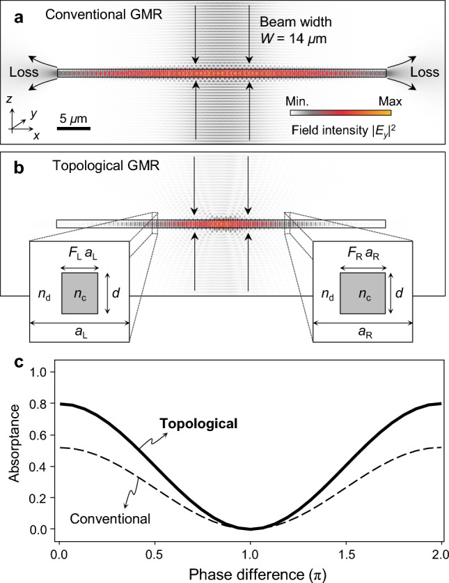
We first consider a conventional GMR CPA device in order to describe our proposed approach in comparison. In Fig. 1a, we show a conventional GMR CPA device and its resulting field distribution, respectively. We assume thickness d = 500 nm, core refractive index nc = 3.485 (α-Si), clad refractive index nd = 2.45 (Si3N4), period a = 540 nm, and fill factor F = 0.45 in this calculation. In addition, we include intrinsic loss of α-Si at 0.0052, which is reasonable from experimental data in the literature19,20. We use the finite element method (FEM) for the numerical analyses. See Method section for details of the simulation conditions.
Figure 1.

Basic concept of a topological GMR CPA. (a,b) Electric field intensity |Ey|2 distributions in the CPA operation for conventional and topological GMRs with footprint size 50 μm, Gaussian beam width W = 14 μm under normal incidence of TE-polarized light at wavelengths 1468 and 1493 nm, respectively. (c) Enhanced phase-sensitive absorptance-modulation profile of the topological GMR CPA device in comparison with the conventional GMR at the critical coupling condition.
This trial device induces a critically-coupled GMR at wavelength 1468 nm under normal incidence of transverse-electric (TE)-polarized light and thereby it can function as a CPA device under planewave incidence in principle. For two coherent Gaussian-beam incidences with beam width 14 μm, an incomplete CPA with its absorptance degraded down to ~ 50% is obtained. The imperfection is significant and originates in two major factors—in-plane leakage losses and modal mismatch between the incident field and resonance mode. In a fundamental viewpoint, these two factors are inevitable because GMR states are basically delocalized Bloch–Floquet states with its coupled radiation modes being planewaves with infinite width in general. Consequently, conventional GMR CPA devices are highly sensitive to sizes of a device or incident beam.
A topological-junction GMR device can considerably alleviate or even completely remove these issues, as shown in Fig. 1b. We assume a junction of two topologically distinguished waveguide gratings with parameters FL = 0.35, aL = 560 nm, FR = 0.45, and aR = 540 nm with subscripts L and R denoting the left and right side of the junction, respectively. This parameter set is derived such that the two gratings about the junction have opposite Dirac-mass signs, which are determined by a formal mapping of the photonic wave equation onto the one-dimensional Dirac equation for relativistic elementary particles16.
In Fig. 1b, we assume the identical coherent Gaussian-beam incidences at wavelength 1493 nm. No in-plane leakage loss is observed and the guided-mode field is well confined within the incident beam region, implying better mode match. Subsequently, the absorptance is improved up to 80%. In Fig. 1c, we compare the phase-sensitive absorptance-modulation profiles of the conventional and topological-junction cases. We note that the proposed topological junction structure can enhance the absorptance peak up to almost 100%, as we will demonstrate in the next section.
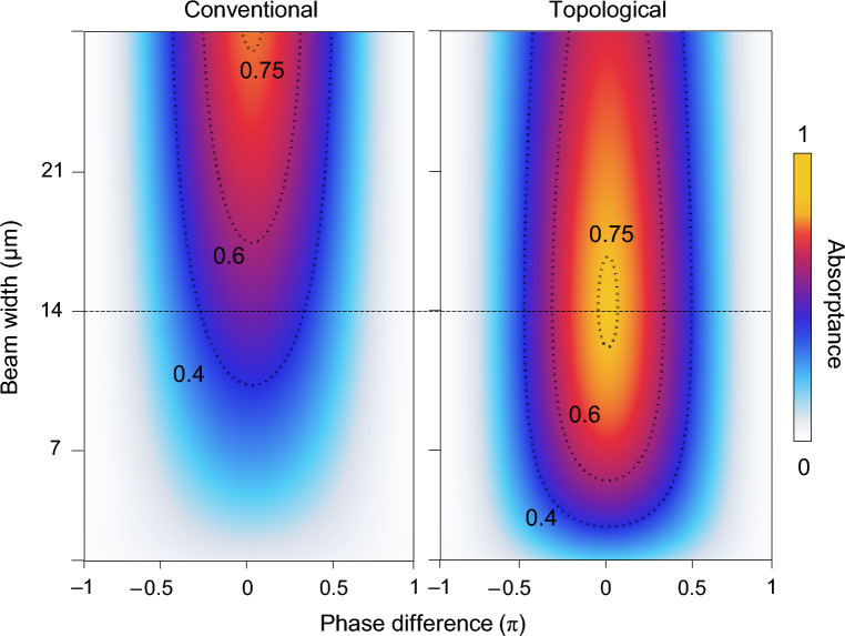
We further investigate the finite beam-width effect on the coherent absorption properties for the conventional and topological junction structures. Figure 2 shows the phase-sensitive absorptance change for the Gaussian beam width varying from 2 to 28 μm. The absorptance is modulated by the interference while the phase difference between the incident beams are changing from − π to π. The modulation depth depends on the incident beam width. For the conventional GMR case, the modulation depth increases with the beam width (W) because the ideal point is obtained for the infinitely wide beam, i.e., planewave. In contrast, the topological junction case has its largest modulation-depth point at W = 14 μm for our particular design. This optimal beam-width condition is obtained when the incident beam profile best matches to the localized GMR state at the junction. The effect of finite beam size is closely related to angular tolerance of a resonance. In our case here, we identify an angular-tolerance width as angular full-width at half-maximum of a resonance peak. The calculated angular-tolerance widths for the conventional GMR at off-normal-incidence and normal-incidence conditions are 0.16° and 0.8°, respectively. These values are substantially smaller than the topological junction structure which has 1.6° for the angular-tolerance width. We also note in the small beam-width region below 14 μm that the large modulation depth domain is much more persistent for the topological junction case, which is highly desirable for compact device development.
Figure 2.
Impact of finite beam width on the performance. Incident-beam-width-dependent absorptance modulation profiles for the conventional and topological GMR CPA devices in Fig. 1. Footprint size of the devices is fixed at 50 μm.
Topological mode-matching method
In analogy to the zero-energy state solution of the Dirac equation, a junction of two topologically distinguished lattices supports a leaky JR state16,17 at the center of the bandgap. In such structures, optical near-field and radiation patterns of this leaky JR state can be conveniently described, using the formal analogy of the photonic coupled-mode theory to the one-dimensional Dirac equation. The theory describes the transversal electric field for the JR state as a localized standing wave
| 1 |
where u(z) is the cross-sectional wave function of the guided mode, G = 2π/a is the grating vector, and fJR(x) = is the lateral envelope function of the JR state with m denoting the Dirac mass parameter. Consequently, Eq. (1) describes the localized state part ψJR of the total electric field, which is confined within the guided-mode envelope function u(z). Note that a π/2 phase difference between two standing guided modes u(z)eiGx and iu(z)e–iGx arises due to the phase delay from the Bragg reflection processes, respectively. As previously discussed in Ref.18, fJR(x) also describes the beam envelope of the coupled leakage-radiation distribution fleak(x), i.e., fleak(x) = fJR(x). The relation between fleak(x) and Dirac-mass distribution m(x) can be alternatively expressed as
| 2 |
Equation (2) provides a convenient method for the complete mode match essential for the ideal CPA operation. An essential condition for the ideal CPA state is to have coherent incident beams configured such that they are the exact time-reversal of the leakage-radiation from the localized mode. This implies that fleak(x) must be matched to the incident beam profile for the ideal CPA state. In this perspective, a complete mode match can be obtained for a given arbitrary incident beam profile finc(x) by configuring m(x) according to Eq. (2) with the mode-matching condition finc(x) = fleak(x).
In experimental situations, obtaining the mode-matching condition finc(x) = fleak(x) is possible in two opposite ways in general. One is to carefully configure finc by means of available beam-shaping methods. The other is to configure fleak by means of nanophotonic structure optimizations. The latter is desirable in many practical situations, where finc is predetermined by the specific choice of sources and other required conditions. However, configuring a desired fleak is basically nontrivial and involves tedious numerical optimizations that often do not ensure an ideal solution. The topological GMR CPA device with Eq. (2) takes a remarkable advantage within this context.
The mode-matching condition by means of Eq. (2) can be conveniently obtained by appropriately designing unit-cell geometry. For a rectangular grating-ridge unit cell of our interest here, the Dirac mass is determined primarily by fill-factor F of the grating as
| 3 |
where sinc(x) = sinc(πx)/(πx) is the normalized sinc function, Δε = nc2–nd2 is the dielectric constant contrast in the grating layer, ng is the group index of the guided mode, λ0 is the bandgap center wavelength, and C1 and C2 are dimensionless constants associated with the strength of the first- and second-order diffraction processes, respectively17. Therefore, we can systematically configure fleak(x) = finc(x) for a given arbitrary finc(x) by taking fill-factor distribution F(x) according to Eqs. (2) and (3).
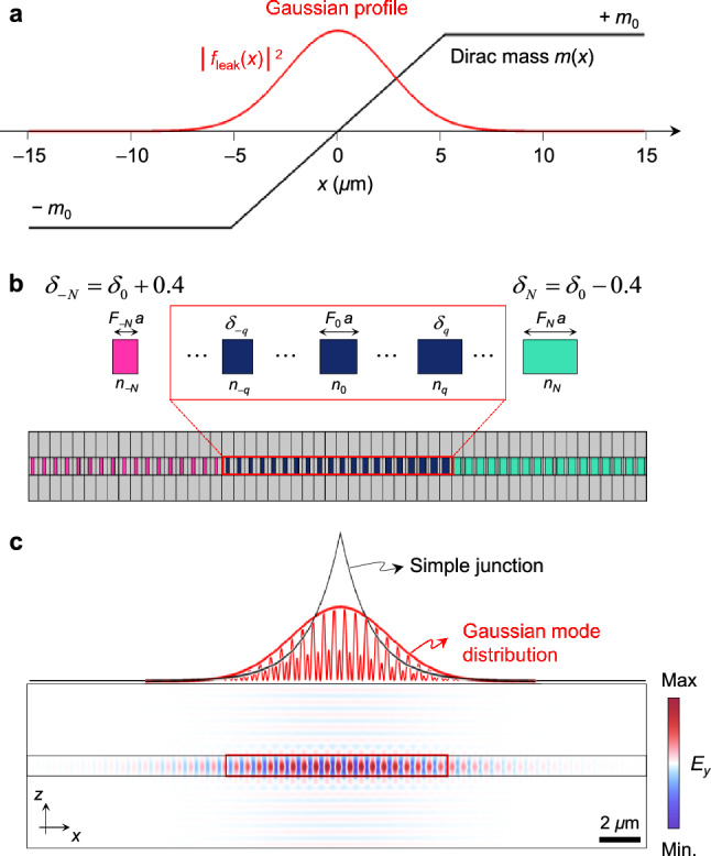
We numerically demonstrate this topological mode-matching method for a most popular beam shape—Gaussian beam. For the trial case of Fig. 1b, we assume a piece-wise constant Dirac-mass distribution, i.e., m(x < 0) = − m0 and m(x > 0) = + m0, where m0 > 0. We refer to this case as “simple junction” hereafter. Thereby, the leakage radiation has a bidirectional decaying-exponential beam profile, which is not matched quite well to the Gaussian beam and results in the incomplete CPA at 80%. We provide an example that the lost 20% efficiency is almost completely recovered by means of the topological mode-matching method.
Equation (2) implies a linear m(x) distribution for a Gaussian fleak profile, as shown in Fig. 3a. We design each unit cell for such m(x) distribution by introducing a cell-by-cell parameter δq = δ0 − qΔ, where q is unit-cell index running over − N to + N, δ0 is a critical point for m = 0, and Δ is constant increment, as shown in Fig. 3b. For the sake of convenience in this proof-of-concept demonstration, parameter δq simultaneously tunes nc and F of the q-th unit cell such that ncq = nd + δq and fill factor Fq = (navg − nd)/δq with navg = F0 nc0 + (1 − F0)nd. Equation (3) for Eq. (2) is conveniently mapped onto the unit cell geometry in this way.
Figure 3.

Topological mode-matching to a Gaussian beam. (a) Dirac mass m(x) distribution for the mode-matching condition in Eq. (2) with an exemplary Gaussian beam. (b) Schematic of a mode-matched topological junction structure. (c) Electric field Ey pattern of the JR state in the mode-matched structure in comparison with the simple junction structure.
The result is provided in Fig. 3c. The design parameters are δ0 = 1.035, Δ = 0.04, N = 10, α = 4.4 × 10⁻³, nd = 2.45, navg = 2.864, a = 550 nm, and d = 500 nm. These parameters are optimized for a Gaussian JR-state envelope with beam diameter 9.4 μm. We show the mode-matched Gaussian envelope in comparison with the simple junction case where m(x) is piece-wise constant at − m0 for x < 0 and + m0 for x > 0, of which values correspond to the cell-by-cell parameter δ0 + 0.3 and δ0 − 0.3. The 2D field distribution of the JR state for the mode-matched junction is provided below.
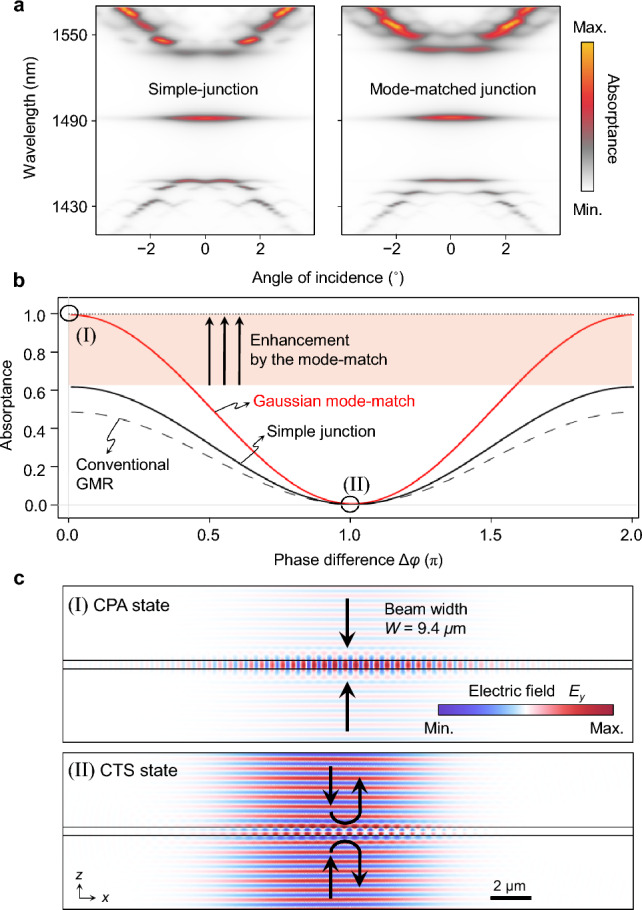
The resonance band structure and phase-sensitive control performance of the mode-matched junction structure is shown in Fig. 4 in comparison with the simple-junction case. In Fig. 4a, we show angle-dependent coherent-absorption spectra for simple junction and mode-matched junction. We clearly identify the JR-state resonance in the middle of the bandgap region for both cases. See Method section for details of simulation conditions. The phase-sensitive absorptance modulation profile under a Gaussian beam incidence is provided in Fig. 4b. The mode-matching results in a remarkable performance enhancement from those for the simple-junction JR-state and conventional GMR cases, where parameter δ for the conventional GMR case is constant at δ0 − 0.3. Note that the area illuminated by the incident beam profile finc(x) and the linear m(x) distribution for a Gaussian fleak(x) profile must be aligned, so that they are ideally mode-matched in the excitation area. At the in-phase excitation condition (Δφ = 0) with 9.4-μm-wide Gaussian incident beams, the absorptance becomes almost perfect at A = 0.989 when compared to A = 0.616 and 0.473 for the simple-junction JR-state and conventional GMR cases, respectively. Importantly, such a high efficiency is obtained for a remarkably small footprint size at 30 μm. In this comparison, the peak absorptance for the simple junction structure can be slightly enhanced up to 63% by reducing the beam width down to 8.5 μm. Thereby, the case provided in Fig. 4b is a near-optimal condition for the simple junction structure.
Figure 4.

Almost ideal performance enabled by a mode-matched topological GMR CPA device. (a) Angle-dependent absorption spectra for the simple and mode-matched junction spectra. (b) Phase-sensitive absorptance-modulation profiles of mode-matched junction structure in comparison with the conventional GMR and simple-junction cases. We assume coherent light incidence of 9.4-μm-wide Gaussian beams. (c) Electric field patterns at the in-phase CPA (I) and out-of-phase CTS (II) states.
The mode-matched JR-state device enables highly efficient optical modulation between the CPA and CTS states by tuning the incoming phase difference from 0 to π as indicated by I (Δφ = 0) and II (Δφ = π) in Fig. 4b. Corresponding field distributions are shown in Fig. 4c. At the CPA state, strong excitation of the mode-matched JR state and no out-going wave are clearly observable. At the CTS state in contrast, the JR state is not excited due to the complete destructive interference in the resonance mode while the complementary constructive interference happens in the out-going wave field, leading to the complete scattering with no absorption. Therefore, this device can function as a compact coherent perfect absorber without any significant performance degradation in the previous conventional approaches.
The remarkable enhancement of the performance by mode matching suggests that the device performance should be sensitive to spatial alignment of the incident beam position with the junction center. The sensitivity can be inferred by considering spatial correlation, i.e., normalized spatial overlap, between the incident beam profile and JR-state envelope. In the spatial-correlation approach, the alignment tolerance can be roughly determined in a similar sense to the Rayleigh criterion for diffraction-limited optical resolution. Accordingly, the lateral tolerance width Δxc for in-plane alignment must be half-width at half-maximum WJR/2 of the JR state envelope, i.e., Δxc ≈ WJR/2. For out-of-plane alignment along the surface normal axis, the axial tolerance region Δzc must be depth of beam waist, which corresponds to the Rayleigh range in case of Gaussian beams, i.e., Δzc ≈ (πλ−1)WJR2. For ideal performance, the lateral and vertical alignment errors Δx and Δz should be substantially smaller than Δxc and Δzc, respectively. In our simulated case for Fig. 4, Δxc ≈ 4.9 μm and Δzc ≈ 50 μm. This implies that sub-micron level (~ Δxc/10) precision is required for lateral alignment while micron-scale (~ Δzc/10) precision is enough for vertical alignment in order to obtain ideal performance.
Discussion
In conclusion, we have proposed a topological-junction coherent perfect absorber taking advantages of small device footprint and persistently high performance. Characteristic field distributions of a leaky JR state at the junction lead to efficient mode-matching to incident Gaussian beams. On this basis, we numerically demonstrate 30-μm-wide CPA device with almost ideal interferometric control of absorption and scattering of coherent incident beams with 10-μm diameter. Such properties are hardly available with the conventional GMR structures. Therefore, our result strongly encourages further extensive follow-up study including higher-order JR states for complete two-dimensional confinement and subsequent adoptable mode matching as well as practical applications to low-power optical modulators, light-electricity transducers, coherence filters, sensors, and many others.
In particular, absolute absorptance values at the CPA and CTS states are crucial in practice. Considering the responses in Fig. 4b for example, the modulation depth in the transmitted coherent signal between the CPA and CTS states is 19.5 dB for the beam-shaped topological junction, which is remarkably higher than 4.1 dB for the simple-junction case and 2.7 dB for the conventional GMR case. If we further consider coherence filter applications, impact of such modulation depth contrast is also significant. Suppose a coherence filter system that transmits coherent signal while rejecting incoherent noises below a certain required level, let’s say 10% of the incident noise. For this, we have to set the operation condition at the CTS state so that the coherent signal absorption is minimal. The incoherent absorptance is simply given by 0.5Amax, where Amax is the absorptance at the CPA state. We then estimate the minimal number Nd of devices in a serial connection and absolute efficiency η of the transmitted coherent signal. We obtain Nd = 4 and η = 93% for the beam-shaped topological junction whereas Nd = 10 and η = 84% for the conventional GMR performing the same incoherent noise rejection capability. Besides such efficiency-wise comparison, the topological junction device is highly desirable in consideration of robustness against structural imperfections and errors, which are unavoidable in experiments. Although we do not provide detailed analyses for our particular cases treated, it is previously known well from Ref.16 that spectral location and resonance strength of a topological-junction GMR are insensitive to random parametric errors in the structural parameters such as grating ridge width and period.
Methods
The calculation domain for supercell structure which consists of multiple of unit-cell elements was covered with perfect matched layers (PML) with the scattering boundary condition. The phase-sensitive absorptance profiles were calculated by surface integration of total power dissipation density for the supercell computational domain. The mode-matched Gaussian JR-state in Fig. 3c was obtained using the time stationary eigenfrequency solver for the supercell with the PML boundary condition. In the calculation of the angle-dependent absorption spectra, we use the same supercell computational domain and apply the periodic boundary condition to the lateral boundaries of the supercell.
Acknowledgements
This research was supported in part by the Leader Researcher Program (NRF-2019R1A3B2068083) and NRF Sejong Science fellowship (NRF-2022R1C1C2006290).
Author contributions
C.Y.P., K.Y.L., and J.W.Y. conceived the original concept. C.Y.P., K.Y.L., and J.W.Y. developed the fundamental theory. C.Y.P. and K.Y.L. performed the numerical analyses. All authors discussed the results. C.Y.P. and J.W.Y. wrote the manuscript. C.Y.P. and K.Y.L. contributed equally to this work.
Data availability
All data needed to evaluate the conclusions during this study are present in this paper. Request for additional information should be addressed to J.W.Y. at yoonjw@hanyang.ac.kr.
Competing interests
The authors declare no competing interests.
Footnotes
Publisher's note
Springer Nature remains neutral with regard to jurisdictional claims in published maps and institutional affiliations.
These authors contributed equally: Chan Young Park and Ki Young Lee.
References
- 1.Chong YD, Ge L, Cao H, Stone AD. Coherent perfect absorbers: Time-reversed lasers. Phys. Rev. Lett. 2010;105:053901. doi: 10.1103/PhysRevLett.105.053901. [DOI] [PubMed] [Google Scholar]
- 2.Wan W, et al. Time-reversed lasing and interferometric control of absorption. Science. 2011;331:889–892. doi: 10.1126/science.1200735. [DOI] [PubMed] [Google Scholar]
- 3.Baranov DG, Krasnok A, Shegai T, Alù A, Chong Y. Coherent perfect absorbers: Linear control of light with light. Nat. Rev. Mater. 2017;2:17064. doi: 10.1038/natrevmats.2017.64. [DOI] [Google Scholar]
- 4.Yoon JW, Song SH, Magnusson R. Critical coupling in dissipative surface-plasmon resonators with multiple ports. Opt. Express. 2010;25:25702–25711. doi: 10.1364/OE.18.025702. [DOI] [PubMed] [Google Scholar]
- 5.Zanotto S, Bianco F, Miseikis V. Coherent perfect absorption and transparency in lossy and loss/gain metasurface-embedding structures. Proc. IEEE Int. Conf. Transparent Opt. Netw. 2017 doi: 10.1109/ICTON.2017.8025114. [DOI] [Google Scholar]
- 6.Pu M, et al. Ultrathin broadband nearly perfect absorber with symmetrical coherent illumination. Opt. Express. 2012;20:2246–2254. doi: 10.1364/OE.20.002246. [DOI] [PubMed] [Google Scholar]
- 7.Zhang J, et al. Coherent perfect absorption and transparency in a nano structured graphene film. Opt. Express. 2014;22:12524–12532. doi: 10.1364/OE.22.012524. [DOI] [PubMed] [Google Scholar]
- 8.Yoon JW, Koh GM, Song SH, Magnusson R. Measurement and modeling of a complete optical absorption and scattering by coherent surface plasmon-polariton excitation using a silver thin-film grating. Phys. Rev. Lett. 2012;109:257402. doi: 10.1103/PhysRevLett.109.257402. [DOI] [PubMed] [Google Scholar]
- 9.Zhu W, Xiao F, Ming K, Premaratne M. Coherent perfect absorption in an all-dielectric metasurface. Appl. Phys. Lett. 2016;108:121901. doi: 10.1063/1.4944635. [DOI] [Google Scholar]
- 10.Quaranta G, Basset G, Martin OJF, Gallinet B. Recent advances in resonant waveguide gratings. Laser Photon. Rev. 2018;12:1800017. doi: 10.1002/lpor.201800017. [DOI] [Google Scholar]
- 11.Huang L, Xu L, Powell DA, Padilla WJ, Miroshnichenko AE. Resonant leaky modes in all-dielectric metasystems: Fundamentals and applications. Phys. Rep. 2023;1008:1–66. doi: 10.1016/j.physrep.2023.01.001. [DOI] [Google Scholar]
- 12.Boye RR, Kostuk RK. Investigation of the effect of finite grating size on the performance of guided-mode resonance filters. Appl. Opt. 2020;39:3649. doi: 10.1364/AO.39.003649. [DOI] [PubMed] [Google Scholar]
- 13.Gambino F, Giaquinto M, Ricciardi A, Cusano A. A review on dielectric resonant gratings: Mitigation of finite size and Gaussian beam size effects. Results Opt. 2022;6:100210. doi: 10.1016/j.rio.2021.100210. [DOI] [Google Scholar]
- 14.Kazarinov RF, Henry CH. Second-order distributed feedback lasers with mode selection provided by first-order radiation loss. IEEE J. Quantum Electron. 1985;21:144–150. doi: 10.1109/JQE.1985.1072627. [DOI] [Google Scholar]
- 15.Rosenblatt D, Sharon A, Friesem AA. Resonant grating waveguide structures. IEEE J. Quantum Electron. 1997;33:2038–2059. doi: 10.1109/3.641320. [DOI] [Google Scholar]
- 16.Lee KY, et al. Topological guided-mode resonances at non-Hermitian nanophotonic interfaces. Nanophotonics. 2021;10:1853–1860. doi: 10.1515/nanoph-2021-0024. [DOI] [Google Scholar]
- 17.Lee KY, Yoon S, Song SH, Yoon JW. Topological beaming of light. Sci. Adv. 2022;8:eadd8349. doi: 10.1126/sciadv.add8349. [DOI] [PMC free article] [PubMed] [Google Scholar]
- 18.Zhang J, MacDonald KF, Zheludev NI. Controlling light-with-light without nonlinearity. Light Sci. Appl. 2012;1:e18. doi: 10.1038/lsa.2012.18. [DOI] [Google Scholar]
- 19.Giese JA, et al. Guided-mode resonant coherent light absorbers. Opt. Lett. 2014;3:486–488. doi: 10.1364/OL.39.000486. [DOI] [PubMed] [Google Scholar]
- 20.Fannin AL, et al. Experimental evidence for coherent perfect absorption in guided-mode resonant silicon films. IEEE Photon. J. 2016;8:6802307. doi: 10.1109/JPHOT.2016.2552160. [DOI] [Google Scholar]
Associated Data
This section collects any data citations, data availability statements, or supplementary materials included in this article.
Data Availability Statement
All data needed to evaluate the conclusions during this study are present in this paper. Request for additional information should be addressed to J.W.Y. at yoonjw@hanyang.ac.kr.


