Abstract
Advances in high-efficiency solar cells introduce photon management challenges, including the difficult texturization of flat surfaces and low photon utilization at short wavelengths. While bifacial crystalline silicon solar cells have a front pyramid structure and SiNx layers reduce reflections, managing photons on the flat backside remains a challenge. To enhance light utilization, a soft nanoimprint technique was utilized to create pyramid micro-structured polyurethane films doped with europium (Eu3+) complex. These films, which possess anti-reflection and down-conversion properties, can be applied externally to various high-efficiency solar cells without compromising electrical performance. Research on the backside of bifacial PERC solar cells revealed that the optimal composite functional film increases the integrated current by 5.70%, with a 1.27% gain from down-conversion effects. This specialized film presents a novel approach to interface matching for different types of solar cells.
A composite functional film with a random positive-pyramidal light-trapping structure and down-conversion capabilities has been prepared by the soft nanoimprint technique to enhance light utilization for solar cells.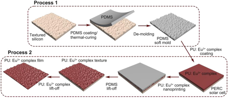
1. Introduction
Crystalline silicon solar cells currently dominate the market, accounting for over 90% of the market share. This dominance is attributed to their high photoelectric conversion efficiency (PCE) and cost-effectiveness.1 Improving photoelectric conversion efficiency further can be achieved through two approaches. First, effectively passivating internal and surface interfaces to increase minority carrier lifetimes. Second, increasing the incident light amount through methods such as texture structure and anti-reflective films, which is also a key focus area for researchers.2 As an indirect bandgap semiconductor, silicon exhibits relatively poor light absorption capabilities, particularly in the near-infrared region.3 Furthermore, over 30% of incident light is lost due to reflection at short wavelengths. Consequently, optical losses due to low absorption at long wavelengths and high reflection at short wavelengths limit the number of photons that can be converted into electricity in silicon solar cells. Typically, a textured surface featuring randomly distributed micron-scale positive pyramids is fabricated on the surface of crystalline silicon. This extends the optical path length and effectively compensates for the low absorption coefficient. Additionally, SiNx layers with varying silicon/nitrogen ratios (typically 2–3 layers) are used to further minimize light reflection.4
To further improve the conversion efficiency of silicon solar cells, researchers have developed some new solar cell structures. One of the most promising technologies is the bifacial passivated emitter and rear cell (bi-PERC), which adopts aluminum grid lines on the back to replace the conventional full aluminum backfield structure. This technology harnesses solar energy from both front and back surfaces, significantly enhancing energy utilization and reducing electricity costs.5 However, the back surface's lack of texture still causes substantial light reflection, despite Al2O3 and SiNx layers for passivation and anti-reflection. Furthermore, for some flat cells that are not ideal for surface texturization, such as perovskite, silicon/perovskite tandem and other thin film solar cells, it is imperative to develop advanced textured surfaces to reduce reflectivity. Numerous random and periodic nanostructures, such as nanowires,6–8 nanopillars,9–11 nanocones,12–14 nanoneedles15–17 and nanospheres18–20 have been extensively studied as back reflectors or front anti-reflection layers. The gradual change in the effective refractive index from the top to the bottom of these nanostructured textures, similar to multi-layer anti-reflection films, enhances light trapping throughout the visible spectrum.21 However, the introduction of nanostructures with high specific surface area on silicon surfaces can induce defects and promote surface recombination,22 limiting their practical use.
On the other hand, the primary factor limiting solar cell efficiency is the mismatch between the solar cell's absorption bandgap and the incident solar spectrum.23 The spectral response of crystalline silicon solar cells is concentrated in the visible region, while ultraviolet (UV) and infrared (IR) radiation, comprising about 50% of solar radiation, cannot be effectively utilized for photoelectric conversion. Moreover, PV modules encapsulated with glass and EVA still experience degradation under ultraviolet radiation, especially for heterojunction solar cells passivated with amorphous silicon. Lanthanide ions,24 such as Eu3+,25 Sm3+,26 Tb3+ 27 and Dy3+,28 have distinctive 4f electronic configurations that enable UV light absorption and visible light emission.29 Specifically, it includes the following two points. Shielding effect: The 4f orbital is deeply buried in the inner layer and is shielded by the outer 5s and 5p orbitals, with less influence from crystal field effects. In this way, the electronic energy levels of the 4f orbital are relatively fixed and less susceptible to external environmental interference. Transition effect: the 4f–4f transition is usually a forbidden transition, which means that the transition probability is low, but the energy level of the emitted light is relatively stable and not easily affected by external factors. This characteristic allows them to emit stable light even after prolonged excitation. This positions them as excellent candidates to enhance UV spectral response and protect solar cells from UV degradation, thus improving conversion efficiency. However, rare earth elements possess a rich set of f-orbitals; however, due to the Laporte forbidden rule that prohibits transitions between f-orbitals, these ions exhibit limited absorption capacity for UV and visible light, resulting in low luminescence efficiency.30 Organic ligands coordinated with lanthanide ions form complexes that compensate for the weak absorption of down-conversion ions, significantly enhancing luminescence.31 Nevertheless, down-conversion ions require a specific thickness for effective UV absorption and cannot be directly doped into silicon wafers. Currently, down-conversion ions doping in EVA encapsulant is employed,32 but its high cost prevents large-scale application.
In response to these challenges, this study introduces a novel photon management strategy using Eu3+ complex-doped pyramidal micro-structured polyurethane (PU:Eu3+ complex) films with anti-reflection and down-conversion properties. The incorporation of random positive pyramids structures can enhance the propagation path of incident light within the photovoltaic material, thereby reducing light reflection and increasing light capture. Lanthanide ions (such as Eu3+) have also been repeatedly applied in photovoltaic cells, demonstrating their effective role in down-conversion processes. The film is designed to be affixed onto the SiNx layer and electrode gridlines of backside of the commercial bi-PERC monocrystalline silicon solar cell. The polyurethane material's refractive index is adjusted to meet the optical requirements between the SiNx and EVA layers. This thin film not only achieves texturization on the backside of PERC cells to enhance photon utilization but also facilitates the effective conversion of 300–400 nm UV light into visible wavelengths to reduce UV attenuation. The nano/micro-structure of the film can be customized through template design to further enhance light incidence. It can also be applied to flat solar cell surfaces as a replacement for traditional texturing, making it suitable for silicon/perovskite tandem and other thin film solar cells. Our research group has successfully fabricated various nanostructured polyurethane films via nanoimprinting, demonstrating strong anti-reflection performance.33 This work aims to further incorporate down-conversion functions into polyurethane films to investigate their optical management capabilities.
2. Material and methods
2.1. Materials
Ethanol, m-Xylylene Diisocyanate (XDI), dibutyltin dichloride, triethoxy-1H,1H,2H,2H-tridecafluoro-n-octylsilane were purchased from Aladdin, europium(iii) nitrate hexahydrate (Eu(NO3)3·6H2O) was purchased from HX-R, 4,7-diphenyl-1,10-phenanthroline was purchased from Meryer, 4-mercaptomethyl-3,6-dithia-1,8-octanedithiol (GST) was purchased from Wengjiang Reagent, polydimethylsiloxane (PDMS, DC 184 DOW SIL) was from Dow Corning. All chemicals were used without further purification. The commercial pyramid-textured solar cells, used as original hard templates, were purchased from CHINT SOLAR and first cut into pieces (3 cm × 3 cm). Soft templates were prepared using PDMS. Nanoimprint lithography was used to prepare the anti-reflective and down-conversion structure on the backside of the commercial bi-PERC mono-crystalline silicon solar cells.
2.2. Preparation of Eu3+ complex
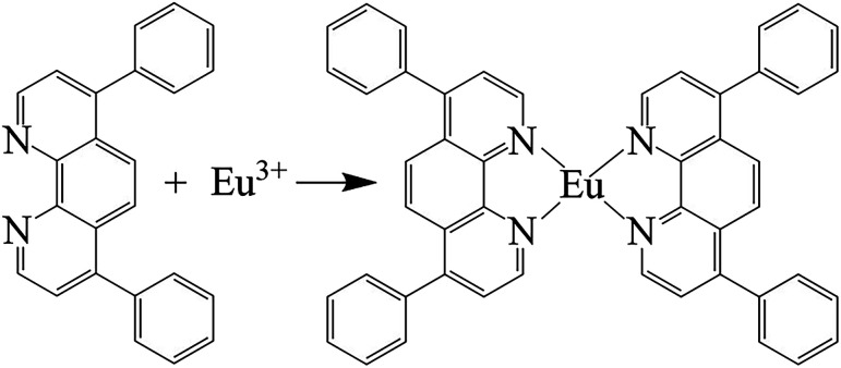
We follow the method described by Dai Songyuan.30 Firstly, 4,7-diphenyl-1,10-phenanthroline (2 mmol) and Eu(NO3)3·6H2O (1 mmol) were fully dissolved in 20 mL of ethanol, respectively. A white Eu3+ complex precipitate was formed after slowly adding Eu(NO3)3·6H2O solution to 4,7-diphenyl-1,10-phenanthroline solution with constant stirring. The reaction process is shown in Fig. 1. After stirring for 30 min, the complex was then purified by centrifugation and washed several times with ethanol and then dried at 40 °C.
Fig. 1. Schematic illustration of the reaction of Eu3+ with organic complex to form Eu3+ complex.
2.3. Preparation of PDMS soft templates
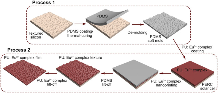
Triethoxy-1H,1H,2H,2H-tridecafluoro-n-octylsilane was diluted to a concentration of 0.5% in ethanol, and the pH was adjusted to the range of 4–5 to prepare an anti-adhesive solution. Textured solar cells were immersed in this solution for 10 minutes, allowing for the self-assembly of a molecular layer on the surface to impart hydrophobic and anti-adhesive properties. To transfer the pyramidal structure through the PDMS soft template, DC184 was mixed (main agent : hardener = 10 : 1, mass ratio) and stirred thoroughly to replicate the morphology. The mixed solution was then spin-coated onto the surface of the solar cell with random positive pyramids morphology that had undergone anti-adhesive treatment, and cured in a vacuum oven at 60 °C for 6 h. The obtained PDMS film was peeled off from the template, resulting in a soft template with a random micron-scale inverted-pyramidal morphology surface. The preparation process is schematically shown in process 1, Fig. 2.
Fig. 2. Schematic illustration of transfer random positive-pyramidal morphology to PU:Eu3+ complex film.
2.4. Preparation of PU:Eu3+ complex composite functional film
To prepare an uncured PU solution, we followed the method described by Zhang Guiming:34 dibutyltin dichloride (2 mg) was added to XDI (1 g) to form a mixture. The above mixture (0.2 g) was then added to XDI (1.19 g) and stirred in an ice bath for 10 minutes. Followed by the addition of GST (1.28 g) which was stirred for an additional 5 minutes. Different ratios (1 wt%, 2 wt%, 3 wt%, content higher than 3 wt% caused coagulation of the sol) of the as-prepared Eu3+ complex was added and the obtained mixed solution was transferred to a vacuum oven and degassed for 10 min to obtain uncured PU solutions with a molar ratio of GST : XDI = 2 : 3 while also possessing down-conversion properties, which was marked as PU:Eu3+ complex-1 wt%, PU:Eu3+ complex-2 wt% and PU:Eu3+ complex-3 wt%, respectively.
Commercial bi-PERC solar cells were used as the substrates for soft nanoimprint lithography. Before the process, the solar cells were washed with a mixed solution with a volume ratio of acetone : ethanol : H2O = 1 : 1 : 1 for 15 minutes, followed by ultrasonic cleaning in DI water. The mixed PU solution was spin-coated onto the backside surface of the cleaned solar cells at a rotational speed of 1000 rpm. The patterned PDMS soft template was then attached to the PU solution, applying a pressure of 10 N to allow sufficient infiltration. A thermal nanoimprinting process was carried out under 120 °C for 2 h to complete curing. The textured PU:Eu3+ complex composite functional films were obtained after removing the PDMS. The film is also self-supporting and can be easily adhered to various flat solar cell surfaces. The preparation process is schematically shown in process 2, Fig. 2.
2.5. Characterization
The surface morphologies of textured silicon, patterned PDMS, imprinted PU:Eu3+ complex film, as well as cross-sectional morphologies and the energy dispersive X-ray spectroscopy (EDX) of imprinted PU:Eu3+ complex film were all investigated by scanning electron microscopy (GeminiSEM 300, Zeiss). The UV-vis-NIR reflectance spectra were recorded at the wavelength range of 300–1100 nm using the U-4100 spectrophotometer (HITACHI). The photoluminescence emission (PL) and excitation (PLE) spectra were measured with a fluorescence spectrometer (FLSP920). The external quantum efficiency (EQE) spectrum was measured with a quantum efficiency measurement instrument (QEX10). The photovoltaic parameters of the PERC cell were investigated by the solar cell current–voltage (J–V) characteristic curve measurement system (IV5, PV measurement) under the illumination of AM 1.5 G (100 mW cm−2).
3. Results and discussion
3.1. Morphology and composition of the films
In previous studies, we successfully fabricated anti-reflection films featuring diverse morphologies using multiple templates.33 In this study, we use a random pyramid-textured template alongside the nanoimprint method to fabricate PU-based anti-reflection films. Furthermore, we investigate the effect of doping with down-conversion materials on the performance of solar cells.
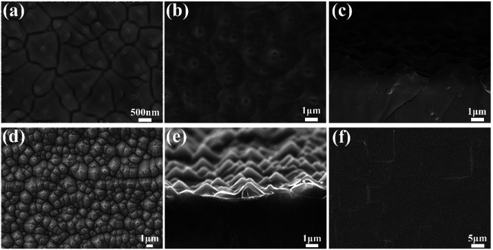
A silicon wafer featuring a micro-scale, random positive-pyramidal morphology acts as the master template for soft nanoimprint. The SEM image of this surface is shown in Fig. 3(a). Notably, the large-scale, randomly distributed structures (ranging in length from 0.5 μm to 2 μm) are obtained through anisotropic etching of Si wafer by alkaline solution. The master template is durable, allowing repeated use without degradation in standard processes. SEM images of the PDMS soft template's surface and cross-section are shown in Fig. 3(b) and (c), respectively. This template was created by transferring the morphology from the original silicon template. The SEM images for both the surface and cross-section of the PU:Eu3+ complex films, prepared via soft nanoimprint using the PDMS soft templates, are shown in Fig. 3(d) and (e). Notably, it can be observed that the random positive-pyramidal morphology of the silicon template has been perfectly replicated.
Fig. 3. SEM image of (a) the surface of textured silicon master template, (b) the surface of PDMS soft template, (c) the cross-section of the PDMS soft template, (d) the surface of PU:Eu3+ complex-3 wt% film, (e) the cross-section of PU:Eu3+ complex-3 wt% film and (f) the backside of bi-PREC solar cell.
3.2. Photoluminescence analysis of the films
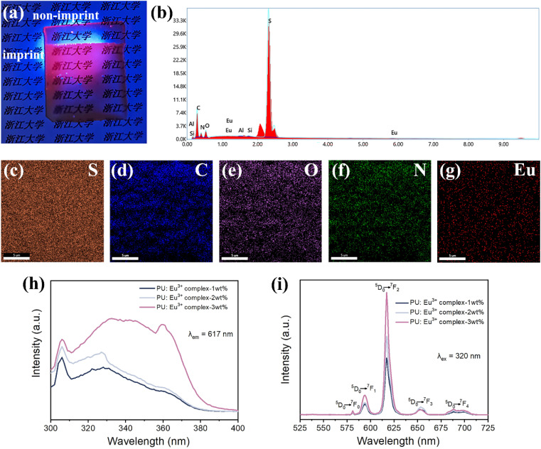
Upon exposure to a 365 nm UV lamp, the PU:Eu3+ complex film exhibits red luminescence and boasts excellent light transmittance, as shown in Fig. 4(a). Meanwhile, an EDX spectroscopy analysis of the PU:Eu3+ complex film on a PERC solar cell identifies S, C, O, and N in the PU matrix, and Si, Al in the silicon wafer. A trace amount of europium (Eu) is also identified, confirming the successful doping of Eu3+ complex into the PU film. These results are shown in Fig. 4(b)–(g). The presence of sulfur (S), originating from GST, contributes to the PU matrix's elevated refractive index within the visible spectrum, clocking in at 1.64 at 500 nm, which was observed in our previous study.33
Fig. 4. (a) Digital photography of PU:Eu3+ complex-3 wt% film when exposed to UV light at 365 nm, (b) EDX spectrum, (c) S, (d) C, (e) O, (f) N and (g) Eu element distribution map of the surface of PU:Eu3+ complex-3 wt% film, the photoluminescence (h) excitation and (i) emission spectra of PU:Eu3+ complex films (Eu3+ complex content: 1, 2, and 3 wt%).
Upon irradiation of the films with excitation light at 320 nm, the highest emission peak was observed at 617 nm, and the excitation spectrum at 617 nm was measured subsequently, with the results depicted in Fig. 4(h) and (i). The increase in concentration of Eu3+ complex in PU film is accompanied by a gradual increase in excitation and emission spectral intensity. The Eu3+ complex concentration is limited at 3 wt% to avoid increases in viscosity affecting nanoimprint operations. Heightened excitation in the 300–400 nm band confirms the PU:Eu3+ complex's UV absorption capabilities. Furthermore, the composite functional film shows multiple photoluminescence peaks at wavelengths of 581, 594, 617, 653, and 688 nm. These peaks correspond to electron transitions from 5D0 → 7F0, 5D0 → 7F1, 5D0 → 7F2, 5D0 → 7F3, and 5D0 → 7F4, respectively, as shown in Fig. 4(i).30 The emission spectra reveal the characteristic red luminescence of Eu3+ under UV excitation.
3.3. Anti-reflection and down-conversion effect of the film, and photovoltaic performance of solar cells
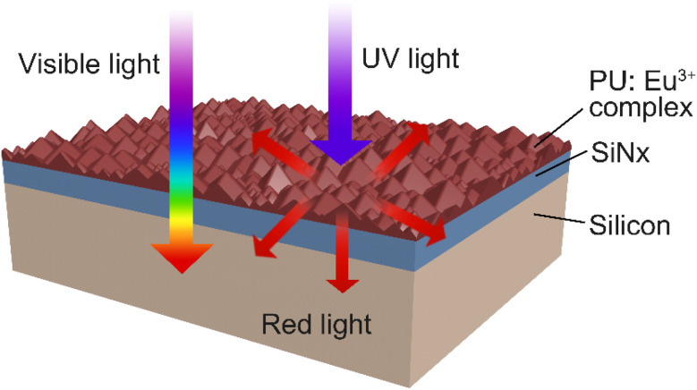
The backside of the bi-PERC solar cell, depicted in Fig. 3(f), is flat and lacks light-trapping structures. This surface is coated with an Al2O3/SiNx layer for passivation and anti-reflection, complemented by a metallic grid applied through screen printing. The PU:Eu3+ complex composite functional film is fabricated on this backside to investigate its anti-reflection and photon down-conversion abilities, as illustrated in Fig. 5. The film's textured pyramidal surface features are designed to repeatedly reflect and refract sunlight, thereby facilitating enhanced solar incidence in a broad wavelength spectrum. In addition, high-energy photons, are absorbed by the film and converted into lower-energy photons to implement the application of short-wavelength photons. This down-converted red light is more readily absorbed by the solar cell, thereby improving the short-circuit current and conversion efficiency.
Fig. 5. Schematic illustration of down-conversion mechanism of PU:Eu3+ complex film coated silicon solar cell.
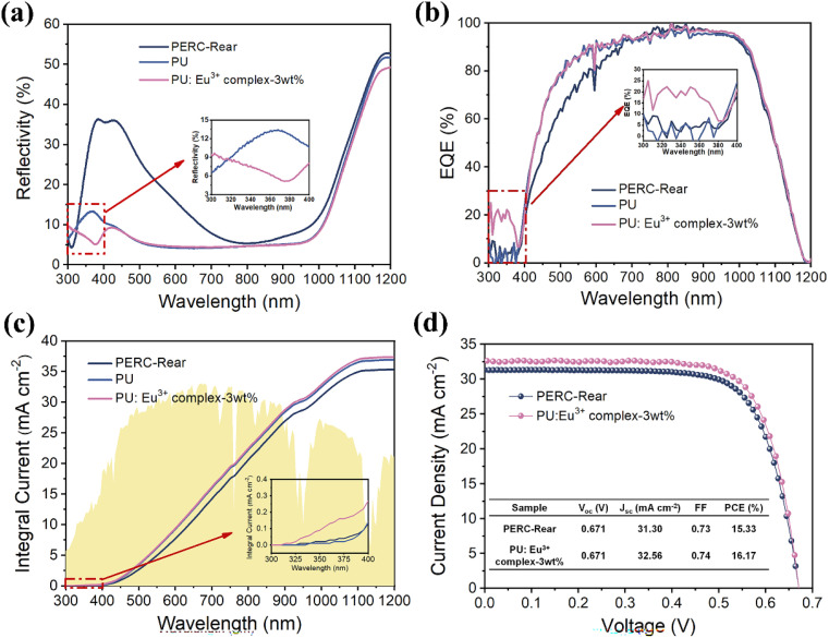
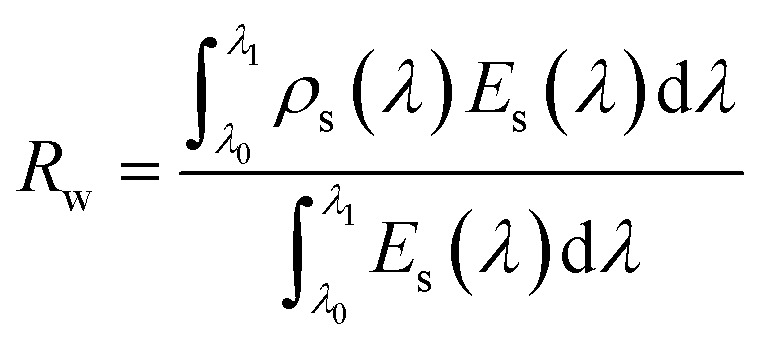
The spectra in Fig. 6(a) show that the weighted average reflectivity (Rw) of different samples. Rw of the sample in a specific band is calculated according to the following equations (where Rw, λ0, λ1, ρs, Es are weighted average reflectivity, initial wavelength, cut-off wavelength, reflectance for a specific wavelength, solar spectral radiation density at AM 1.5 G):
 |
1 |
Rw of the backside surface of the bi-PERC solar cell is 20.40%. Notably, a PU film with random positive pyramids reduces this reflectivity to 8.44%. Moreover, the Rw further decreases to 7.50% at a 3 wt% Eu3+ complex concentration in the PU film. The Eu3+ complex's effect is greatest in the 300–400 nm range, due to the film's improved UV absorption and reduced reflections.
Fig. 6. (a) Reflectance spectra, (b) EQE spectra and (c) integral current density spectra of bi-PERC solar cells coated with PU film and PU:Eu3+ complex-3 wt% film on the backside (the inset shows the magnified spectra of 300–400 nm band), (d) J–V curves of bi-PERC solar cells with PU:Eu3+ complex-3 wt% film on the backside.
To investigate the effect of PU:Eu3+ complex film on the photoelectric performance of solar cells, EQE spectra were analyzed with illuminations from backside, as shown in Fig. 6(b). The EQE improvement provided by the PU film without Eu3+ complex is mainly limited to the 400–700 nm wavelength band, due to its positive-pyramidal surface's anti-reflection properties. The EQE curves of these cells displayed similar profiles within the wavelength range of 400 to 1200 nm, attributed to the non-absorption of the Eu3+ complex. On the contrary, PU films with Eu3+ complexes significantly enhance the EQE of solar cells due to enhanced light absorption in the 300–400 nm range.
The integral current density is calculated according to the following equations (where JSC, λ0, λ1, F(λ), and EQE(λ) are integral current density, initial wavelength, cut-off wavelength, solar spectral photon flux at AM 1.5 G and EQE value at specific wavelengths).
 |
2 |
The integral current density spectra shown in Fig. 6(c) indicate that JSC increases from 35.42 mA cm−2 to 37.44 mA cm−2 when coated with PU:Eu3+ complex film. PU:Eu3+ complex film at 3 wt% concentration has a relative total gain of 5.70% relative to rear-PERC and a relative down-conversion gain of 1.27% relative to PU film, underscoring the value-added benefit of incorporating Eu3+ complex into the PV design, as illustrated in Table 1.
R w and JSC of the backside of bi-PERC solar cells and backside coated with PU film and PU:Eu3+ complex film (Eu3+ complex content: 1, 2, and 3 wt%).
| Rear-PERC | PU | PU:Eu3+ complex-1 wt% | PU:Eu3+ complex-2 wt% | PU:Eu3+ complex-3 wt% | |
|---|---|---|---|---|---|
| R w (%) | 20.40 | 8.44 | 8.14 | 7.86 | 7.50 |
| J SC (mA cm−2) | 35.42 | 36.99 | 37.03 | 37.22 | 37.44 |
| Relative gain of JSC (%) to rear-PERC/PU | —/— | 4.43/— | 4.55/0.12 | 5.08/0.65 | 5.70/1.27 |
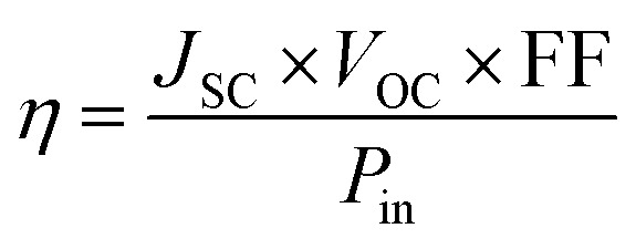
The J–V curves of the backside of bi-PERC solar cells with and without PU:Eu3+ complex film is shown in Fig. 6(d). PCE in the table inserted in the figure is calculated according to the following equations (where η, JSC, VOC, FF and Pin are photoelectric conversion efficiency, short-circuit current density, open-circuit voltage, fill factor and power density of the incident photon, respectively).
 |
3 |
It can be seen that VOC and FF of the cell exhibit negligible change, indicating that PU:Eu3+ complex film does not alter the Fermi energy distribution in the solar cell's p–n junction. At 3 wt% Eu3+ concentration, JSC rises from 31.30 mA cm−2 to 32.56 mA cm−2 and PCE rises from 15.33% to 16.17%, reaching a relative enhanced PCE of 5.45%. This suggests that the geometrical trapping of the randomly distributed positive-pyramidal structure increases the utilization of incident photons, while the addition of Eu3+ complex improves the efficiency of UV utilization and provides extra red photons for absorption by the silicon cell, leading to an observed enhancement of photocurrent in the J–V curve. It is worth noting that the JSC measured by the J–V curve (Fig. 6(d)) is lower than that calculated by EQE (Table 1). This discrepancy is probably due to the presence of leakage current from the surrounding area during the J–V measurement.
Moreover, the existing down-conversion layers currently for solar cells include halide nanocrystals, rare earth ion phosphors, carbon or graphene quantum dots, compound quantum dots, etc. (Table 2). The synthesized Eu3+ complex in this study exhibits advantages of a simple synthesis method, abundant raw material source, and remarkable down-conversion effect, providing a new technological pathway for commercialization of down-conversion for solar cells.
Comparison of down-conversion materials to increase efficiencies of solar cells.
| Type of solar cell | Downconverter used | Excitation (nm) | Emission (nm) | Increase of PCE (%) | Relative gain (%) | Reference |
|---|---|---|---|---|---|---|
| Silicon solar cell | CsPbCl1.5Br1.5:Yb3+, Ce3+ nanocrystals | 365 | 400–500, 988, 1540 | From 18.1 to 21.5 | 18.8 | 35 |
| Mono-crystalline silicon solar cells | Ce3+–Yb3+ co-doped YAG phosphors | 460 | 500–700, 900–1100 | From 13.18 to 13.82 | 4.9 | 36 |
| Hybrid solar cell | Graphene quantum dots (GQDs) | 373 | 415 | From 11.50 to 13.22 | 15.0 | 37 |
| Mono-silicon solar cell | CdO nanotips (NTs) | 512 | 695 | From 12.1 to 13.8 | 14.0 | 38 |
| Bi-PERC solar cell | Eu3+ complex | 320 | 581, 594, 617, 653, and 688 | From 15.34 to 16.14 | 5.45 | This work |
4. Conclusion
In this study, a composite functional film with a random positive-pyramidal light-trapping structure and down-conversion capabilities has been successfully prepared by the soft nanoimprint technique. The film is specifically designed for integration onto the backside of bi-PERC solar cells without additional surface texturing. When the textured PU film is doped with 3 wt% Eu3+ complex, it reduces the Rw value to 7.50%, which is superior to rear-PERC without a down-conversion layer (20.40%). This demonstrates the film's effectiveness in reducing light reflection. The micro-scale anti-reflection structure, which consists of randomly distributed positive-pyramidal structures, provides a geometric light-trapping effect. Additionally, the photon conversion of Eu3+ complex converts UV photons into red photons. This yields a maximum total gain of 5.70% and a down-conversion gain of 1.27% for the integrated current of solar cells. A relative enhanced PCE of 5.45% was achieved when coated with a PU:Eu3+ complex film. In addition, the light capture structure on the surface of the thin film can be customized by controlling the template to further enhance its anti-reflection properties. This innovative approach is promising for next-generation, high-efficiency solar cells that are incompatible with traditional acid–alkali textured structures. This is especially relevant for solar cells like perovskite/c-Si tandem and multi-layer perovskite tandem, which face surface texturing challenges and UV degradation problems.
Data availability
The data that support the findings of this study are available from the corresponding author, upon reasonable request.
Author contributions
Sijia Jin and Shengxuan Wang: conceptualization, data curation, formal analysis, investigation and writing-original draft. Hailong Feng: methodology, validation and visualization. Darren He, Alex Hsu, Zhenxing Du, Wei Sun: funding acquisition, investigation, resources. Chunhui Shou, Shien Sun, Deren Yang: funding acquisition, resources, supervision. Haiyan He: project administration, resources and supervision, writing-review & editing. Lei Wang: project administration, funding acquisition, supervision, writing-review & editing.
Conflicts of interest
There are no conflicts to declare.
Acknowledgments
This work was supported by the National Key RD Program of China (No. 2020YFB1506502, 2018YFB1500300), Open Project of Key Laboratory of Solar Energy Utilization & Energy Saving Technology of Zhejiang Province (No. ZJS-OP-2020-01), and Key Project of Zhejiang Province (No. 2021C01170), the Key Research Project of Zhejiang Province (No. 2024C01054).
References
- Hermle M. Feldmann F. Bivour M. Goldschmidt J. C. Glunz S. W. Appl. Phys. Rev. 2020;7:021305. [Google Scholar]
- Tsui K.-H. Lin Q. Chou H. Zhang Q. Fu H. Qi P. Fan Z. Adv. Mater. 2014;26:2805–2811. doi: 10.1002/adma.201304938. [DOI] [PubMed] [Google Scholar]
- Yoshikawa K. Kawasaki H. Yoshida W. Irie T. Konishi K. Nakano K. Uto T. Adachi D. Kanematsu M. Uzu H. Yamamoto K. Nat. Energy. 2017;2:17032. doi: 10.1038/nenergy.2017.32. [DOI] [Google Scholar]
- Han Z. Jiao Z. Niu S. Ren L. Prog. Mater. Sci. 2019;103:1–68. doi: 10.1016/j.pmatsci.2019.01.004. [DOI] [Google Scholar]
- Dullweber T. Schulte-Huxel H. Blankemeyer S. Hannebauer H. Schimanke S. Baumann U. Witteck R. Peibst R. Köntges M. Brendel R. Yao Y. Jpn. J. Appl. Phys. 2018;57:08RA01. doi: 10.7567/JJAP.57.08RA01. [DOI] [Google Scholar]
- Hiralal P. Chien C. Lal N. N. Abeygunasekara W. Kumar A. Butt H. Zhou H. Unalan H. E. Baumberg J. J. Amaratunga G. A. J. Nanoscale. 2014;6:14555–14562. doi: 10.1039/C4NR01914H. [DOI] [PubMed] [Google Scholar]
- Wang Y.-C. Chen C.-Y. Kuo C.-W. Kuan T.-M. Yu C.-Y. Chen I.-C. Phys. Status Solidi A. 2016;213:2259–2263. doi: 10.1002/pssa.201600005. [DOI] [Google Scholar]
- Consonni V. Briscoe J. Kärber E. Li X. Cossuet T. Nanotechnology. 2019;30:362001. doi: 10.1088/1361-6528/ab1f2e. [DOI] [PubMed] [Google Scholar]
- Choi J. Lee T. S. Jeong D. S. Lee W. S. Kim W. M. Lee K.-S. Kim D. Kim I. J. Phys. D: Appl. Phys. 2016;49:375108. doi: 10.1088/0022-3727/49/37/375108. [DOI] [Google Scholar]
- Liu J. Zhang X. Ashmkhan M. Dong G. Liao Y. Wang B. Zhang T. Yi F. Energy Technol. 2013;1:139–143. doi: 10.1002/ente.201200031. [DOI] [Google Scholar]
- Fan Z. Kapadia R. Leu P. W. Zhang X. Chueh Y.-L. Takei K. Yu K. Jamshidi A. Rathore A. A. Ruebusch D. J. Wu M. Javey A. Nano Lett. 2010;10:3823–3827. doi: 10.1021/nl1010788. [DOI] [PubMed] [Google Scholar]
- Zhang D. Ren W. Zhu Z. Zhang H. Liu B. Shi W. Qin X. Cheng C. Nanoscale Res. Lett. 2015;10:9. doi: 10.1186/s11671-014-0718-x. [DOI] [PMC free article] [PubMed] [Google Scholar]
- Vidhya Y. E. B. Vasaa N. J. Manuf. Lett. 2022;33:195–204. doi: 10.1016/j.mfglet.2022.07.026. [DOI] [Google Scholar]
- Jeong S. Garnett E. C. Wang S. Yu Z. Fan S. Brongersma M. L. McGehee M. D. Cui Y. Nano Lett. 2012;12:2971–2976. doi: 10.1021/nl300713x. [DOI] [PubMed] [Google Scholar]
- Makableh Y. F. Nusir A. I. Morris H. McKenzie K. Manasreh O. J. Nanophotonics. 2016;10:046018. doi: 10.1117/1.JNP.10.046018. [DOI] [Google Scholar]
- Wang M. He H. Shou C. Cui H. Yang D. Wang L. Mater. Sci. Semicond. Process. 2022;138:106299. doi: 10.1016/j.mssp.2021.106299. [DOI] [Google Scholar]
- Park K.-T. Guo Z. Um H.-D. Jung J.-Y. Yang J. M. Lim S. K. Kim Y. S. Lee J.-H. Opt. Express. 2011;19:A41. doi: 10.1364/OE.19.000A41. [DOI] [PubMed] [Google Scholar]
- Ha D. Gong C. Leite M. S. Munday J. N. ACS Appl. Mater. Interfaces. 2016;8:24536–24542. doi: 10.1021/acsami.6b05734. [DOI] [PubMed] [Google Scholar]
- Yao Y. Yao J. Narasimhan V. K. Ruan Z. Xie C. Fan S. Cui Y. Nat. Commun. 2012;3:664. doi: 10.1038/ncomms1664. [DOI] [PubMed] [Google Scholar]
- Esmaeilzad N. S. Demir A. K. Hajivandi J. Ciftpinar H. Turan R. Kurt H. Bek A. Adv. Opt. Mater. 2021;9:2000943. doi: 10.1002/adom.202000943. [DOI] [Google Scholar]
- Oh J. Yuan H.-C. Branz H. M. Nat. Nanotechnol. 2012;7:743–748. doi: 10.1038/nnano.2012.166. [DOI] [PubMed] [Google Scholar]
- Abdullah M. F. Alghoul M. A. Naser H. Asim N. Ahmadi S. Yatim B. Sopian K. Renew. Sustain. Energy Rev. 2016;66:380–398. doi: 10.1016/j.rser.2016.07.065. [DOI] [Google Scholar]
- Yu D. Yu T. Lin H. Zhuang S. Zhang D. Adv. Opt. Mater. 2022;10:2200014. doi: 10.1002/adom.202200014. [DOI] [Google Scholar]
- Satpute N. S. Mehare C. M. Tiwari A. Swart H. C. Dhoble S. J. ACS Appl. Electron. Mater. 2022;4:3354–3391. doi: 10.1021/acsaelm.2c00595. [DOI] [Google Scholar]
- Becerro A. I. Allix M. Laguna M. Gonzalez-Mancebo D. Genevois C. Caballero A. Lozano G. Nunez N. O. Ocana M. J. Mater. Chem. C. 2018;6:12830–12840. doi: 10.1039/C8TC04595J. [DOI] [Google Scholar]
- Huerta E. F. Soriano-Romero O. Meza-Rocha A. N. Bordignon S. Speghini A. Caldino U. J. Alloys Compd. 2020;846:156332. doi: 10.1016/j.jallcom.2020.156332. [DOI] [Google Scholar]
- Jin X. Y. Wang Z. Y. Xu H. Y. Jia M. C. Fu Z. L. Mater. Today Chem. 2022;24:100771. doi: 10.1016/j.mtchem.2021.100771. [DOI] [Google Scholar]
- Eliseeva S. Salerno E. Bermudez B. A. L. Petoud S. Pecoraro V. L. J. Am. Chem. Soc. 2020;142:16173–16176. doi: 10.1021/jacs.0c07198. [DOI] [PubMed] [Google Scholar]
- Datt R. Bishnoi S. Hughes D. Mahajan P. Singh A. Gupta R. Arya S. Gupta V. Tsoi W. C. Sol. RRL. 2022;6:2200266. doi: 10.1002/solr.202200266. [DOI] [Google Scholar]
- Jiang L. Chen W. Zhen J. Zhu L. Mo L. Li Z. Hu L. Hayat T. Alsaedi A. Zhang C. Dai S. ACS Appl. Mater. Interfaces. 2017;9:26958–26964. doi: 10.1021/acsami.7b10101. [DOI] [PubMed] [Google Scholar]
- Yang J. W. Kim D. I. Jeong R. H. Park S. Boo J. Int. J. Energy Res. 2022;46:7996–8006. doi: 10.1002/er.7701. [DOI] [Google Scholar]
- Zhou W. Li Y. Zhang R. Wang J. Zou R. Liang H. Opt. Lett. 2012;37:4437–4439. doi: 10.1364/OL.37.004437. [DOI] [PubMed] [Google Scholar]
- Wang S. Cui H. Jin S. Pi X. He H. Shou C. Yang D. Wang L. Heliyon. 2023;9:e20264. doi: 10.1016/j.heliyon.2023.e20264. [DOI] [PMC free article] [PubMed] [Google Scholar]
- Huang S. Zhang G. Du W. Chen H. Polymers. 2021;13:3474. doi: 10.3390/polym13203474. [DOI] [PMC free article] [PubMed] [Google Scholar]
- Zhou D. Liu D. Pan G. Chen X. Li D. Xu W. Bai X. Song H. Adv. Mater. 2017;29:1704149. doi: 10.1002/adma.201704149. [DOI] [PubMed] [Google Scholar]
- Li L. Lou C. Cao H. Diao H. Karunakaran S. K. Appl. Phys. Lett. 2018;113:101905. doi: 10.1063/1.5043221. [DOI] [Google Scholar]
- Tsai M.-L. Wei W.-R. Tang L. Chang H.-C. Tai S.-H. Yang P.-K. Lau S. P. Chen L.-J. He J.-H. ACS Nano. 2016;10:815–821. doi: 10.1021/acsnano.5b05928. [DOI] [PubMed] [Google Scholar]
- Feng W. Liu J. Yu X. RSC Adv. 2014;4:51683–51687. doi: 10.1039/C4RA08328H. [DOI] [Google Scholar]
Associated Data
This section collects any data citations, data availability statements, or supplementary materials included in this article.
Data Availability Statement
The data that support the findings of this study are available from the corresponding author, upon reasonable request.


