Abstract
For two decades, time-resolved transmission electron microscopes (TEM) have relied on pulsed-laser photoemission to generate electron bunches to explore sub-microsecond to sub-picosecond dynamics. Despite the vast successes of photoemission time-resolved TEMs, laser-based systems are inherently complex, thus tend not to be turn-key. In this paper, we report on the successful retrofit of a commercial 200 keV TEM, without an external laser, capable of producing continuously tunable pulsed electron beams with repetition rates from 0.1 GHz up to 12 GHz and a tunable bunch length from tens of nanoseconds down to 10 ps. This innovation enables temporal access into previously inaccessible regimes: i.e., high repetition rate stroboscopic experiments. Combination of a pair of RF-driven traveling wave stripline elements, quadrupole magnets, and a variable beam aperture enables operation of the instrument in (1) continuous waveform (CW) mode as though the instrument was never modified (i.e. convention TEM operation mode, where the electrons from the emission cathode randomly arrive at the sample without resolvable time information), (2) stroboscopic (pump-probe) mode, and (3) pulsed beam mode for dose rate sensitive materials. To assess the effect of a pulsed beam on image quality, we examined Au nanoparticles using bright field, high-resolution TEM imaging and selected area diffraction in both continuous and pulsed-beam mode. In comparison of conventional TEMs, the add-on beam pulser enables the observation of ultrafast dynamic behavior in materials that are reversible under synchronized excitation.
Keywords: TEM, UEM, Stroboscopic, Pulser, Ultrafast
1. Introduction
In the previous two decades, important technological advancements have expanded the range of temporal resolution in transmission electron microscopes (TEM) [1,2]. Direct-counting and single-electron detectors have revealed dynamics in the millisecond timescale, and laser-assisted photoemission microscopes [3] combined with beam scanning, spatially-parsed large area detectors [4], and sparse-sensing algorithms [5], can now unlock phenomena at the μs to femtosecond () timescales. Further optimization of the photoemission stage and beam bunching technologies promise to extend the temporal resolution into the deep and even attosecond regime[6–8].
Beyond pulsed laser-based approach, others have proposed to use dielectric RF cavities to modulate and pulse the electron beam[9–11]. However, a resonant cavity, by definition, operates at a particular resonance frequency; it is not a broadband device and cannot be arbitrarily tuned without significant power loss. The resulting pulsed beam (e.g., the probe beam in a stroboscopic mode) is therefore also single-frequency and not broadly applicable to subjects with dynamic periods beyond the probe frequency. In addition the resonance frequency of a dielectric cavity is known to be prone to thermal drift [12,13], thus additional engineering strategies are required for the probe frequency-drift mitigation.
Advancing our earlier concept paper [14], we recently developed a RF-driven electron beam pulser system and deployed it on a JEOL JEM-2010F TEM (a 200 keV Schottky-emission instrument) [15]. The Pulser is shown in Fig. 1a as the element within the dotted square. The Pulser is inserted between the electron gun and the microscope’s first condenser lens. Its construct is radiation and vacuum compatible with the manufacturer’s requirement. Fig. 1b is a schematic of the internal elements of the Pulser, which consists of three principal elements: electron beam modulator (K1)/demodulator (K2), beam chopping aperture (A), and quadrupole magnets (Q1 through Q3). The incoming CW (unmodified) beam is assumed to enter the Pulser on-optical axis (z-direction), with negligible beam tilt. At the entrance of the Pulser (Z=z0), as the CW beam enters K1, transverse sinusoidal momentum (in the x–y plane) is added to the beam due to the electromagnetic (EM) field within K1. Both K1 and K2 operate in the traveling wave mode, which means in principle, an EM field can be established with any input frequency , but is in practice limited to a passband up to 6 GHz[16]. The transverse force on the incoming electrons depends on the RF phase of K1 at the time of entry.
Fig. 1.
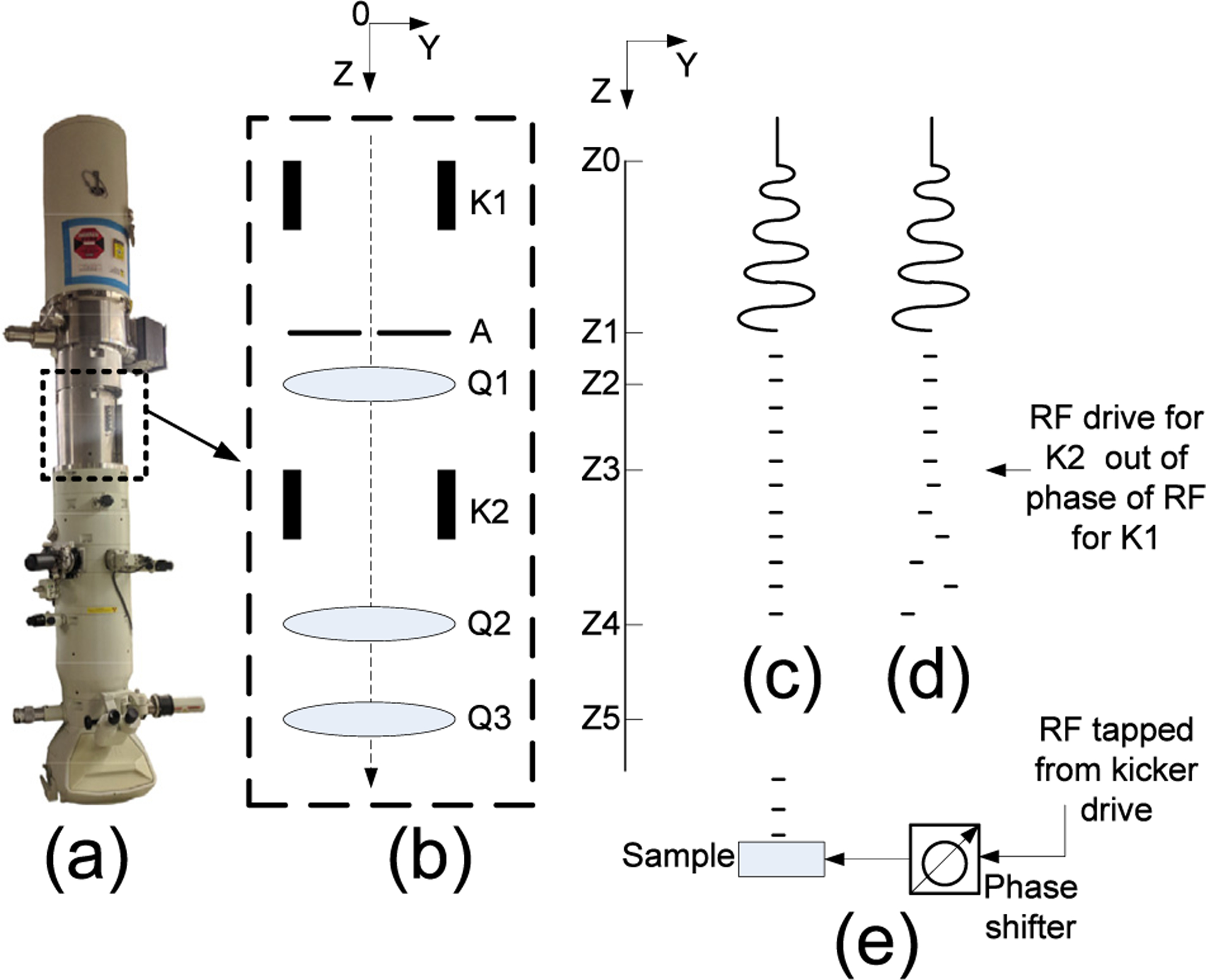
a) A JEM-2010F TEM column with the Pulser (dotted section) inserted between the gun and standard column lens; b) The schematic of the Pulser. K1 and K2 are the modulator and demodulators respectively, A is the beam chopping aperture, Q1, Q2, and Q3 are the quadrupole magnets. Z0 = 0, Z1 = 45 mm, Z2 = 10 0mm, Z3 = 155 mm, Z4 = 180 mm, Z5 = 220 mm); c) schematic of the electron beam in the pulsed beam mode; d) the dual beam mode; e) the strobe mode.
As shown in Fig. 1c and d, the amplitude of the sinusoidal motion grows in a direction along the plane as the modulated beam propagates along the Z axis. After a fixed drift distance, the modulated electron beam enters the beam chopping aperture (A) at . The amplitude of the sinusoidal beam is on the order of 200 μm per 10 W of RF input at 2 GHz based on the simulation which is the upper bound of the aperture size. The aperture partitions the beam into periodic pulses with a frequency of . In the current design, there are five discrete diameters for A, 25μm, 30μm, 35μm, 40μm, and 45μm, which can be used to alter the temporal resolution of the beam. Shorter pulses (better temporal resolution) can be achieved by increasing , the RF amplitude at K1, and/or using a smaller aperture, though using a smaller aperture is the preferred method because increasing K1 amplitude also increases RF power loss in K1, which is dissipated thermally. As the partitioned beam exits , the beam width expands in the Y − Z plane as it propagates in , and both the beam size and divergence will increase. As shown in Fig. 1b, the addition of Q1 and K2 serves to demodulate the beam, and reduce the emittance growth and energy spread (i.e. improve the spatial and temporal coherence of the beam). Downstream of K2 are two more quadrupole magnets Q2 and Q3 which provide additional beam-matching capabilities when coupling into downstream lenses.
2. Working principles of the pulser
By design, the Pulser placement at the gun exit is meant to preserve the original TEM modalities as long as no RF is delivered to the Pulser. When the Pulser is activated, several different operating modes can be selected. In the pulse mode, as shown in Fig. 1c, the Pulser ”chops” the electron beam with a continuously tunable frequency, , from 100 MHz up to 12 GHz. In this mode the duty cycle can be altered independently by adjusting the RF power () delivered to K1. Here, , and can be 10% at 10 W RF input. Note that a recent study showed certain materials are much more tolerant of high accumulated dose under the pulsed beam in comparison to the CW beam [17,18]. Thus a tunable in the pulsed mode would be an important parameter for dose-rate sensitive materials.
The RF input to both K1 and K2 are phase locked to a master oscillator, and generally operate at the same frequency. However, the RF amplitude and phase to K1 and K2 can be independently controlled. In the pulsed beam mode, K2 is in phase with K1, and K2 nullifies the induced transverse momentum of the electrons leaving K1. This is particularly important when a large (> 30 μm) aperture is used. In the dual-beam mode, K2 (at 90° phase lag with respect to K1) adds to the induced transverse momentum of the electrons from K1. The result is two spatially separated pulsed beams, both with the repetition rate of , as illustrated by Fig. 1d. In the dual-beam mode, the electron pulses land in two separate spatial locations (that are temporally out of phase) as observed on the image plane. This mode is primarily used for the characterization of the Pulser, however, it may be possible to probe the specimen at instead of by eliminating one of the twins with an objective aperture.
The most straightforward use case of the Pulser is the stroboscopic mode with pump-probe experiments, which is an extension of the pulsed-beam mode (as shown in Fig. 1e). A daughter RF signal is tapped from the primary K1 drive signal to provide stimulus or ”pump” to the sample through a phase-locked delay line while the sample is probed by synchronized electron pulses. By changing the electrical delay between the pump signal and the probing beam, the complete time evolution of a cyclical dynamic phenomenon can be captured. The full band, 100 MHz < < to 12 GHz, is available in the stroboscopic pumpprobe mode.
The core element enabling the unique capabilities of the Pulser is a novel Traveling Wave Metallic Comb Stripline (TWMCS). The TWMCS operates in a traveling-wave mode, driven by a differential RF signal from one end and terminated at the other end with 50 Ω loads. As shown in Fig. 2a and b, the TWMCS consists of two metallic combs with their teeth facing each other. In this geometry, only the Transverse EM wave mode is allowed to propagate along the beam channel (optic axis). The Transverse EM mode has neither longitudinal electric nor magnetic component, thus in principle no induced energy spread to the incoming beam. As the transverse EM wave propagates, its velocity can be altered by the teeth structure. By optimizing the teeth thickness, spacing, and height, the phase velocity of EM wave can be adjusted to synchronize with the speed of the probe electrons so that they can interact without the phase slippage [19]. As shown in Fig. 2c, the electron momentum and displacement closely track the RF phase when the electron travels through the TWMCS.
Fig. 2.
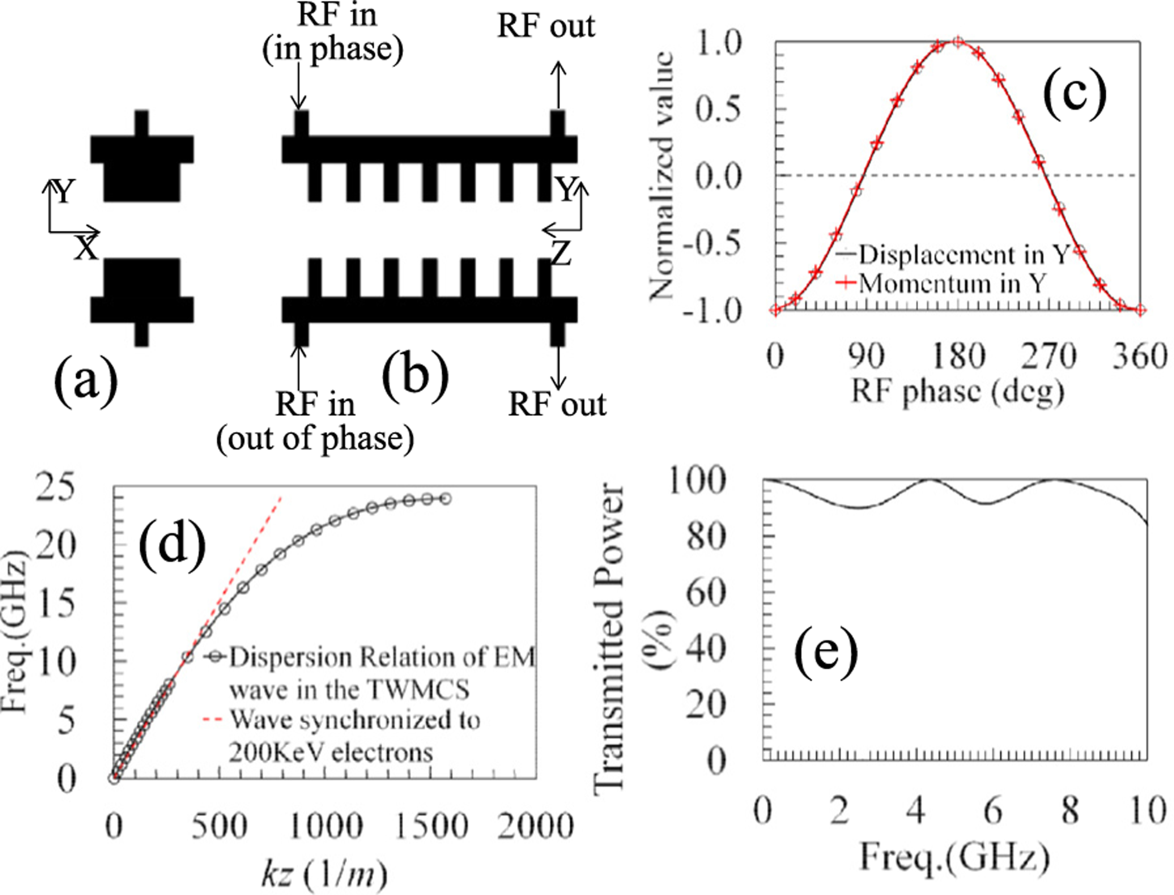
A schematic of the TWMCS: front-view (a) side view (b), with beam traveling along the z direction. (c) The simulated electron displacement vs. theRF phase for an electron traveling through the TWMCS. (d) Comparison the transverse EM wave dispersion in the TWMCS and the linear velocity of a 200 keV electron; e) The simulated RF power transmission coefficient S12 over a 10 GHz span.
Fig. 2 d (black curve) shows the dispersion relation between the wave propagation constant (which represents the phase velocity) and the RF frequency for the transverse EM mode in the TWMCS. The red dotted line is the linear dispersion of a wave with a phase velocity of 0.695c which is the speed of 200 keV electrons. Here, we see that the transverse EM wave in the TWMCS can be synchronized to the 200 keV beam up to . However, matching the high impedance TWMCS to 50 Ω coaxial line over a wide frequency range is nontrivial. Fig. 2e shows the simulated RF power transmission coefficient. The TWMCS is optimized to work at up to 8GHz but in certain frequencies there is only 90% RF power transmission; 10% is reflected back to the power source. Although non-ideal, it will not drastically limit performance.
The beam dynamics of the complete Pulser system were simulated in Astra[15,20]. Fig. 3 shows four simulated cases: (1) K1 on, and no beam chopping aperture (free electron drift until Pulser exit at Z=0.3m); (2) same as (1) but a 25μm aperture was added such that the duty cycle of the chopped beam is approximately 10%; (3) Both K1 and K2 are active and driven by the same voltage (amplitude), and a 25 μm aperture. K2 was phase-matched to K1 (the pulsed beam mode); (4) Same as the case 3 except that the phase of K2 is out-of-phase with K1 (the dual beam mode). The yellow bands denote the location of K1 and K2, the red line indicates the location of the aperture.
Fig. 3.
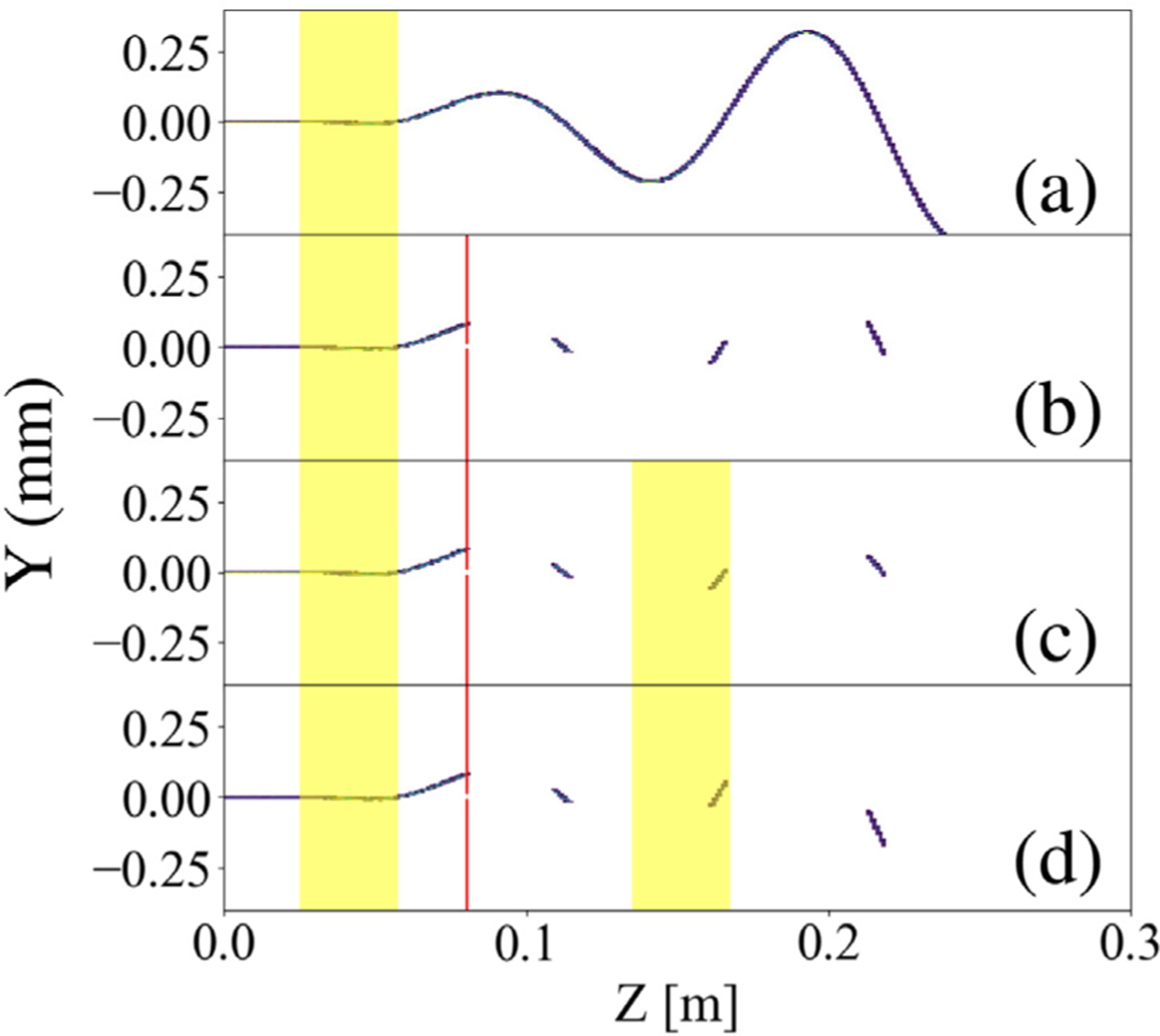
The multi-particle beam simulations produced by Astra. Setup from top: a) K1 on, no beam chopping aperture; b) K1 on, a 25 μm beam chopping aperture, which produced a 10% duty cycle, was inserted.; c) Both K1 and K2 on, running in the pulsed-beam mode; d) Both K1 and K2 on, running in the dual-beam mode. The red vertical line marks the location of the beam chopping aperture. The highlighted stripes mark the locations of K1 and K2. We found that the results from the particle tracking simulations are in excellent agreement with experimental results obtained from an earlier 200 keV electron gun bench test. (For interpretation of the references to colour in this figure legend, the reader is referred to the web version of this article.)
3. Experimental demonstrations of the pulser
In Fig. 4, the tunability of the pulse length was demonstrated by varying the K1 voltage in the dual beam mode. In this mode, the two electron bunches that are nπ apart in time at the exit of the beam chopping aperture are alternately placed near peaks and troughs of the K2 RF drive so that they are transversely kicked in opposite directions. Thus the beam separation distance () as measured on the detector is a reasonable proxy for temporal resolution, and the number of pixels in can be mapped to a time unit. However, the individual electron pulse length cannot be obtained directly from images in the dual-beam mode. For a short pulse length, if it only occupies a small fraction of the RF phase near the peak or trough, most electrons in a pulse experience a similar kicking strength, therefore, their physical size (beam width, ) is less sensitive to the temporal profile. In contrast, for a longer pulse length, is strongly correlated to the real bunch length. For this reason, a clean interpretation of pulse length must be accompanied by particle beam simulations. In Fig. 4a, we plotted the simulated pulse length (blue curve) and its beam width (red curve) on the detector with , K2 at maximum modulation strength, aperture diameter at and varying K1 strength (via the RF calibration to the K1 input terminal). The measured at various K1 strengths are indicated as open circles which overlaid well with the simulated beam width. We then can refer the pulse length indirectly. For example, using the dashed lines drawn in Fig. 4a, we can infer the pulse length is 27 ps.
Fig. 4.
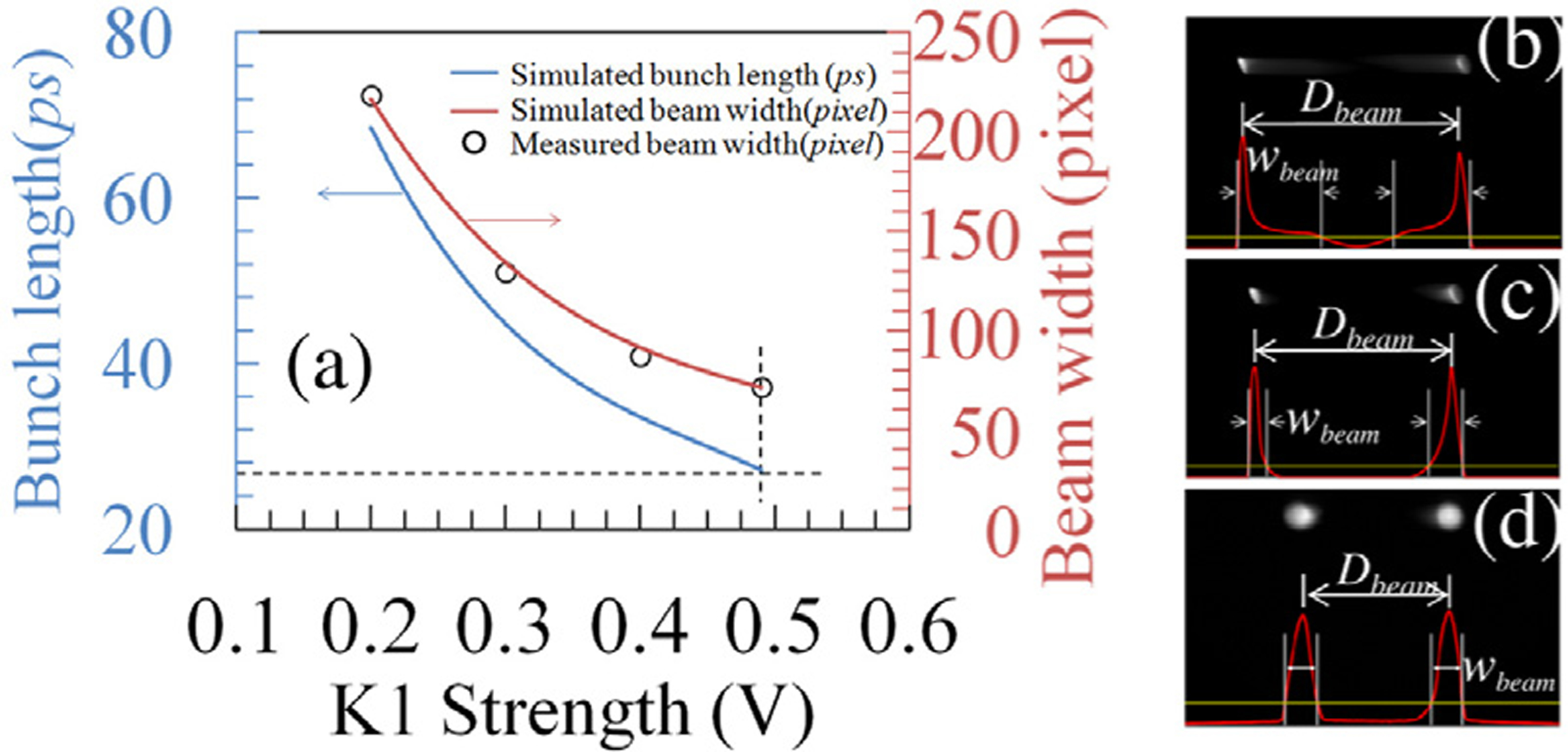
Demonstration of tunability of duty cycle by varying the K1 modulation strength in the dual beam mode with a fixed value of K2. RF drive frequency is 2 GHz (a)–(c) and 5GHz (d). (a) The simulated and measured beam width on the TEM image screen. The captured beam image when K1 strength was set to 0.2V (b), 0.49V (c), 0.3V (d).
Fig. 4 b and c are images acquired at and K1 at 0.2 V and 0.49 V respectively. They also show how was defined d in the measurement. The profiles (red curves) in Fig. 4b and Fig. 4c are not the real beam current profiles. Depending on the RF phase when electrons enter K2, the long tail in Fig. 4b is attributed to both the head and tail of an electron bunch. Therefore, has to include the tail as shown in Fig. 4b and c. It should be pointed out that the values in Fig. 4b and Fig. 4c are supposed to be the same if the pulse arrives at the minima and maxima of K2 drive signal. The slight difference of between Fig. 4b and Fig. 4c is caused by the pulse leading the extrema by 15°, which has been reproduced in the simulation. The electron pulse length at a different frequency, 5 GHz, was also examined (Fig. 4d). 11 ps was measured when K 1strength is set to 0.3V (equivalent to 3W by calibration). Pulse lengths of just a few ps should be achievable by reducing network losses (thus enabling greater power delivery). Alternately, a smaller aperture may be used.
Another way to tune the duty cycle is by varying the diameter of the beam chopping aperture. In the present design, the beam chopping aperture strip contains five aligned holes with different diameters, and it is mounted on piezoelectric X–Y linear stage. In fig. 5, we picked two different diameters ( and ) to demonstrate tunability of the beam duty cycle. In the dual-beam mode, we kept constant at 5 GHz, i.e., the two beamlets are 100 ps apart. The duty cycle, , can be characterized by the ratio of pulse width () over . for is 0.24 in Fig. 5a and is 0.16 in Fig. 5b for . The reduction of duty cycle as a result of changing the aperture size from 40μm to 25μm is 66% which is very close to the ratio of two aperture sizes.
Fig. 5.
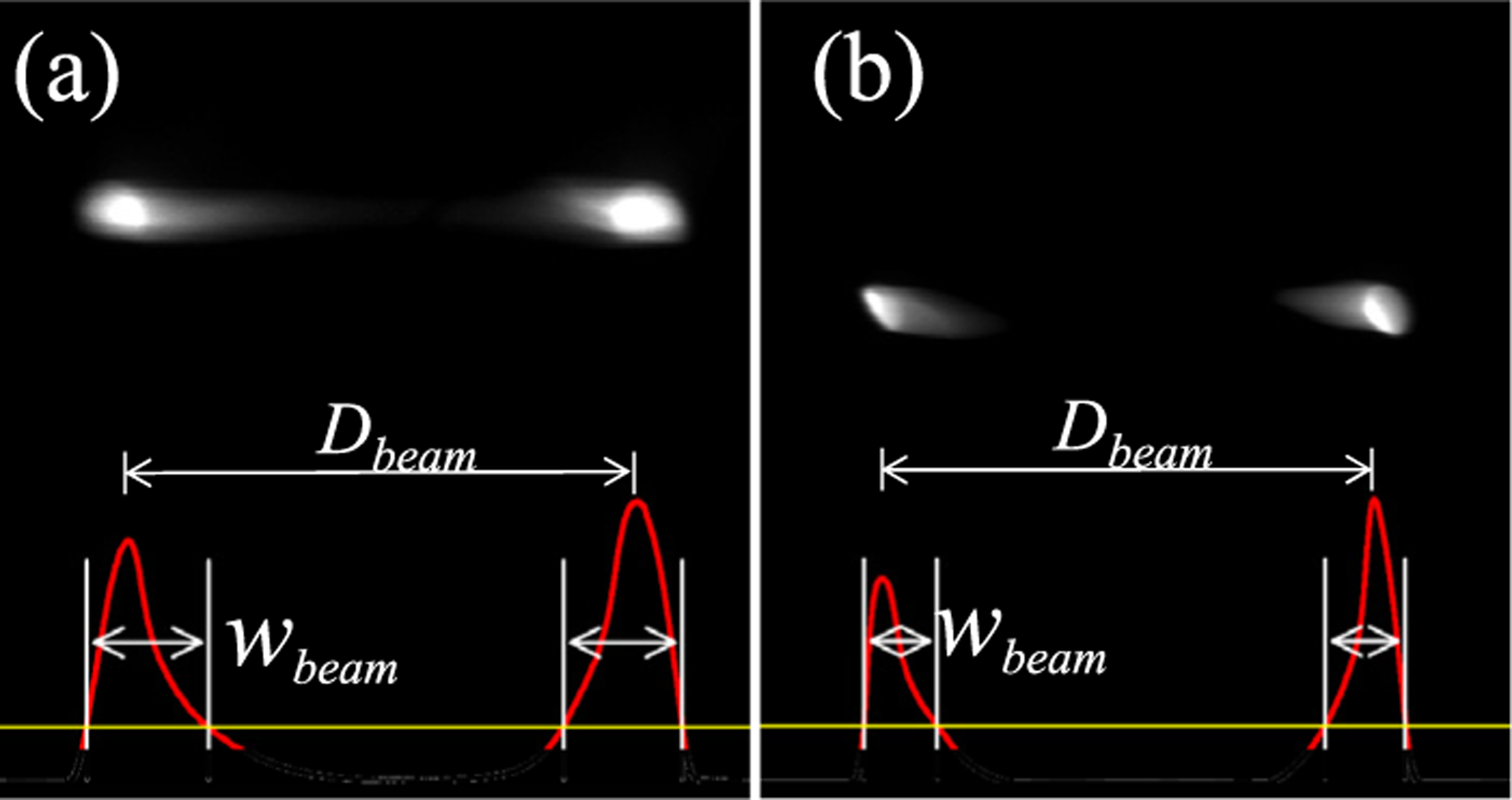
Demonstration of the tunability of duty cycle by varying the aperture size in the dual beam mode: (a) and (b).
Finally, to test the performance of the TEM after the Pulser installation, we acquired bright-field images and diffraction patterns of a standard Au nanoparticle sample using both CW and pulsed-beam modes at (refer to Fig. 6). The choice of 5.2 GHz was arbitrary. Fig. 6a is a bright-field image of Au nanoparticles at an indicated magnification of 200 kX obtained using a CW beam (Pulser off). The morphology of the nanoparticles and the amorphous nature of the carbon support can be seen clearly. We noticed that at a higher magnification of 600 kX, the lattice fringes are still visible in the CW mode (data not shown), suggesting the original spatial resolution of the TEM was not compromised by the Pulser addition. Fig. 6b is another bright-field image of the same area as Fig. 6a, captured under the same imaging condition, same image integration time (2s), but in a modified pulsed-beam mode in which K2 was deactivated (K2 was off due to equipment malfunction during our limited testing window, but it has since been resolved for a different microscope). Nanoparticles are still imaged with reasonable quality. The little contrast blur under the pulsed beam mode is mainly due to the much-lowered electron dose and the possible existence of a small transverse momentum of the pulsed electrons due to an inactive K2. Fig. 6c and d show a comparison of diffraction patterns under the CW and pulsed beam modes with an indicated camera length of 20 cm. All the characteristic Bragg rings of Au nanoparticles can be clearly distinguished in the diffraction patterns under both CW and the modified pulsed-beam modes, and the last ring at 0.57 nm on both diffraction micrographs can be readily resolved, indicating the comparable high quality of diffraction under both operation modes. Again, for the same reasons previously described, the Bragg rings do appear less sharp compared to those produced in CW mode, but the higher spatial frequencies are still preserved. The bright-field imaging and diffraction comparison tests demonstrated that the function and performance of the instrument after the column modification did not exhibit significant changes. Because the RF source, serving as a universal clock, is a versatile electrical signal, the pump (specimen excitation) synchronization using the RF tap can be deployed using a robust ecosystem of specialty specimen holders already in the market place. Therefore, the tunable RF pulsed TEM is potentially a powerful platform for ps-stroboscopic electron imaging and diffraction for exploring ultrafast dynamical processes.
Fig. 6.
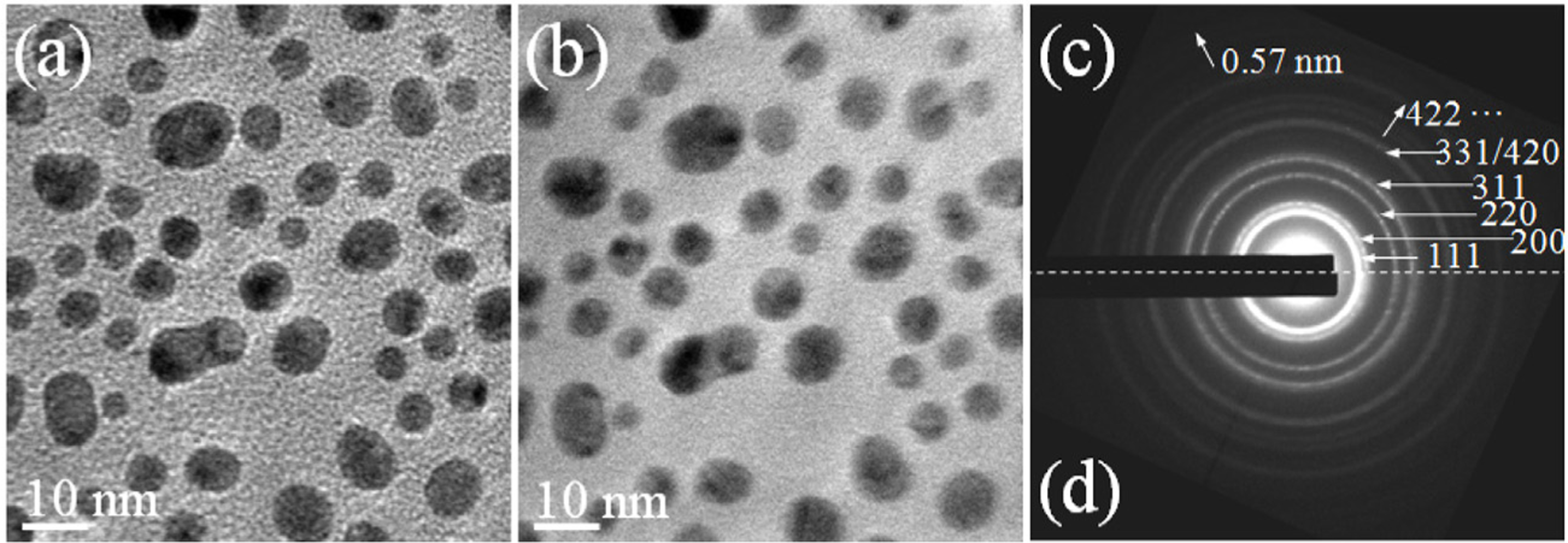
Image and diffraction quality comparison between CW beam and pulsed beam modes using a standard Au nanoparticle sample. (a) TEM image under CW beam mode at a magnification of 200 kX. The exposure time is 2 s; (b) TEM image obtained under the same condition as (a) but using pulsed beam mode. (c) and (d) Selected area diffraction patterns with an indicated camera length of 20 cm under CW beam and pulsed beam modes, respectively.
In conclusion, we have demonstrated a new device which retrofits the conventional TEM and is able to chop the electron beam out of an electrongun at an ultrafast and tunable rate, thus forms electron pulses with nano-seconds to pico-seconds duration and MHz to GHz repetition rate. This device is unique because unlike a microwave cavity, it is broadband tunable. It preserves the original beam coherence, and can return to the conventional modes of operation by simply switching off the Pulser RF control. The ultrashort pulsed electrons in combination with the synchronized sample excitation enables pump-probe experiments including (but are not limited to) ferromagnetic resonance in magnetic materials, magnons, skymions, and atomic measurements in MEMS and NEMS systems.
Acknowledgments
The authors would like to thank JEOL USA for their strong support in accommodating the 200 keV stroboTEM pulser and in its installation, test, and maintenance. The authors also thank Daniel Masiel and Bryan Reed of Integrated Dynamic Electron Solutions for helping to develop the customized TEM column structure to house the Pulser. The work is supported by DOEs SBIR grant under contract DE-SC0013121. Work at BNL was supported by the US DOE-BES, MSED, under Contract No. DESC0012704.
References
- [1].Vanacore G, Fitzpatrick A, Zewail A, Nano Today 11 (2016). [Google Scholar]
- [2].Flannigan D, Zewail A, 4D electron microscopy: principles and applications, Acc. Chem. Res 45 (2012). [DOI] [PubMed] [Google Scholar]
- [3].Lobastov V, et al. , Proc. Natl. Acad. Sci 102 (2005) 7069–7073. [DOI] [PMC free article] [PubMed] [Google Scholar]
- [4].LaGrange T, Reed B, Masiel D, MRS Bulletin 40 (2015) 22–28. [Google Scholar]
- [5].Stevens A, et al. , Advanced Structural and Chemical Imaging 1 (2015). [DOI] [PMC free article] [PubMed] [Google Scholar]
- [6].Feist A, Echternkamp KE, Schauss J, Sergey V SS Yalunin, C. Ropers, Nature 521 (2015) 200–203. [DOI] [PubMed] [Google Scholar]
- [7].Hassan MT, Baskin JS, Liao B, Zewail AH, Nature Photonics 11 (2017) 425–430. [Google Scholar]
- [8].Priebe KE, Rathje C, Yalunin SV, Hohage T, Feist A, Schfer S, Ropers C, Nature Photonics 11 (2017) 793–797. [Google Scholar]
- [9].Verhoevena W, Rensa J, Kieftb ER, Mutsaersa PHA, Luitena OJ, Ultramicroscopy 188 (2018). 185–89 [Google Scholar]
- [10].van Rens JFM, Verhoeven W, Kieft ER, Mutsaers PHA, Luiten OJ, Appl. Phys. Lett 113 (2018) 163104. [Google Scholar]
- [11].Lassise A, Mutsaers PHA, Luitena OJ, Review of Scientific Instruments 83 (2012) 043705. [DOI] [PubMed] [Google Scholar]
- [12].Kajfez D, Guillon P, Dielectric Resonator, Artech House microwave library, Dedham: : Artech House, 1986. [Google Scholar]
- [13].Kajfez D, Chebolu S, Kishk A, Abdul-Gaffoor M, IEEE Transactions on Microwave Theory and Techniques 49 (2001) 80–85. [Google Scholar]
- [14].Qiu J, et al. , Ghz laser-free time-resolved transmission electron microscopy: a stroboscopic high-duty-cycle method, Ultramicroscopy 161 (2016) 130–136. [DOI] [PMC free article] [PubMed] [Google Scholar]
- [15].Certain commercial equipment, instruments, or materials are identified in this paper to specify the experimental procedure adequately. Such identification is not intended to imply recommendation or endorsement by the National Institute of Standards and Technology, nor is it intended to imply that the materials or equipment identified are necessarily the best available for the purpose.
- [16].Jing C, Qiu J, Baryshev SV, Lau JW, Zhu Y, Ultra broad band continuously tunable electron beam pulser, 2016, US20170162361A1, pending. [Google Scholar]
- [17].Kisielowski C, et al. , Discovering hidden material properties of mgcl2 at atomic resolution with structured temporal electron illumination of picosecond time resolution, Advanced Functional Materials (2019) 1807818. [Google Scholar]
- [18].VandenBussche E, Flannigan D, Reducing radiation damage in soft matter with femtosecond timed single-electron packets, ChemRxiv (2019), 10.26434/chemrxiv.8079755.v1. [DOI] [PubMed] [Google Scholar]
- [19].Zhang K, Li D, Electromagnetic Theory for Microwaves and Optoelectronics, Artech House microwave library, Springer Berlin Heidelberg New York, 2015. [Google Scholar]
- [20].Flottmann K, Astra, a space charge tracking algorithm,(Download page). [Google Scholar]


