Abstract
Two-dimensional (2D) van der Waals (vdW) heterostructures are considered as promising candidates for realizing multifunctional applications, including photodetectors, field effect transistors and solar cells. In this work, we performed first-principles calculations to design a 2D vdW MoTe2/MoS2 heterostructure and investigate its electronic properties, contact types and the impact of an electric field and in-plane biaxial strain. We find that the MoTe2/MoS2 heterostructure is predicted to be structurally, thermally and mechanically stable. It is obvious that the weak vdW interactions are mainly dominated at the interface of the MoTe2/MoS2 heterostructure and thus it can be synthesized in recent experiments by the transfer method or chemical vapor deposition. The construction of the vdW MoTe2/MoS2 heterostructure forms a staggered type II band alignment, effectively separating the electrons and holes at the interface and thereby extending the carrier lifetime. Interestingly, the electronic properties and contact types of the type II vdW MoTe2/MoS2 heterostructure can be tailored under the application of external conditions, including an electric field and in-plane biaxial strain. The semiconductor–semimetal–metal transition and type II–type I conversion can be achieved in the vdW MoTe2/MoS2 heterostructure. Our findings underscore the potential of the vdW MoTe2/MoS2 heterostructure for the design and fabrication of multifunctional applications, including electronics and optoelectronics.
Two-dimensional (2D) van der Waals (vdW) heterostructures are considered as promising candidates for realizing multifunctional applications, including photodetectors, field effect transistors and solar cells.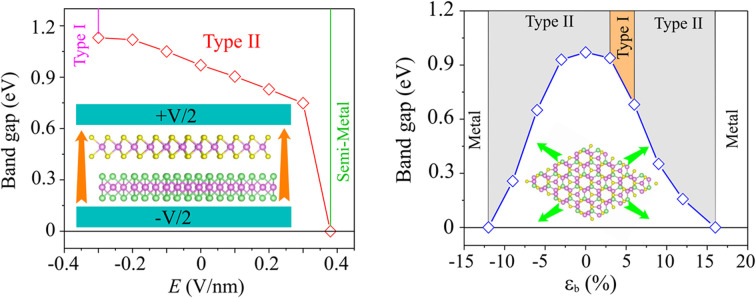
1. Introduction
The advent of two-dimensional (2D) materials, characterized by their atomic structures and unique properties, has ushered in a new era of exploration and innovation in condensed matter physics and materials science. This burgeoning class of materials, with graphene1 as a pioneering example, has captivated both fundamental and industrial researchers. Following the success of graphene, a plethora of 2D materials have been exfoliated and investigated, both in terms of fundamental understanding and practical applications. Recently, the most extensively investigated 2D materials are transition metal mono- and di-chalcogenides,2–5 MXenes6–8 and graphitic carbon nitrides.9–11 The versatility in the electronic and optical properties of 2D materials makes them promising candidates for multiple applications, ranging from advanced electronics to quantum computing and beyond.12–15
More interestingly, the special versatility of 2D materials lies in their potential for creating 2D vdW heterostructures by stacking them together.16–18 The 2D vdW heterostructures based on 2D materials offer an intriguing platform for tailoring and enhancing material properties, unlocking novel phenomena, and paving the way for practical applications in next-generation devices.19–21 Recently, a plethora of 2D vdW heterostructures have been synthesized experimentally and explored computationally, for instance, TMD heterostructures,22,23 MXene heterostructures,24,25 MA2Z4 heterostructures26,27 and phosphorene heterostructures.28–30 Among them, the exploration of vdW heterostructures between different 2D TMD materials has received much more consideration and interest. Many 2D TMD-based vdW heterostructures have been successfully fabricated and explored, such as MoS2/WSe2,31,32 HfS2/MoS2,33 MoS2/WS2,34 MoTe2/ReS2 (ref. 35) and black phosphorus/MoS2.36 One can find that the 2D vdW TMD heterostructures can be synthesized in experiments by various strategies, including top-down37 and bottom-up38,39 strategies.
Recently, a novel 2D vdW heterostructure based on MoTe2 and MoS2 TMD materials has been successfully fabricated in experiments by various methods, such as one-step CVD,40 mechanical exfoliation41,42 and direct imprinting.43 Using the one-step CVD technique, Ding et al.40 fabricated a MoTe2/MoS2 heterostructure and demonstrated that the photodetector based on such a heterostructure exhibits outstanding photoresponsivity and external quantum efficiency. Lately, Ji et al.,41 utilizing mechanical exfoliation, fabricated a 2D vdW MoTe2/MoS2 heterostructure. These findings proved that such a heterostructure can be considered as a promising candidate for optoelectronic devices and integrated photonics. In addition, the MoTe2/MoS2 heterostructure can also be fabricated by combining the mechanical exfoliation and transfer methods42 or direct imprinting.43 All these experimental findings highlighted the potential applications of MoTe2/MoS2 heterostructures for multifunctional devices, including electronics and optoelectronics. Despite experimental successes in the fabrication of MoTe2/MoS2 heterostructures, a comprehensive computational investigation into the depth of their atomic structure, electronic properties and the formation of contact types is notably lacking. Therefore, in this work, we perform first-principles calculations to design a MoTe2/MoS2 heterostructure and investigate its structures and electronic properties and the formation of type II band alignment. The impact of external conditions is also explored to examine the potential applications of the MoTe2/MoS2 heterostructure for multifunctional devices. Our findings underscore the potential of the vdW MoTe2/MoS2 heterostructure for the design and fabrication of multifunctional applications, including electronics and optoelectronics.
2. Computational methods
In this work, the first-principles calculations are performed using the Quantum Espresso simulation package.44,45 The geometric optimization process and electronic property calculations are performed in the framework of the Perdew–Burke–Ernzerhof (PBE) functional46 within the projector augmented-wave (PAW) pseudopotential.47 A cut-off energy of 510 eV and a Monkhorst–Pack (9 × 9 × 1) K-point mesh are employed for all the processes and calculations. The hybrid Heyd–Scuseria–Ernzerhof (HSE) functional48 is also employed to get a more accurate band gap value of materials. The weak vdW interactions that may occur in layered materials can be described by adding the long-range dispersion correction of the Grimme DFT-D3 method.49 The convergence threshold for the force and energy in all the calculations is set at 0.01 eV Å−1 and 10−6 eV, respectively. A vacuum thickness of 27 Å is applied along the z direction of materials to avoid any unnecessary interlayer interactions. A dipole correction is also employed for all the calculation processes.
3. Results and discussion
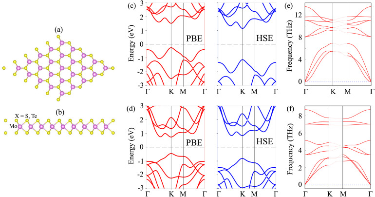
We first investigate the atomic structure and electronic properties of MoX2 (X = Te, S) monolayers. The atomic structures of MoX2 are depicted in Fig. 1. The MoX2 monolayer consists of an X–Mo–X layer, where a Mo atom is sandwiched between two X atoms on different sides. Similar to graphene, the MoX2 monolayer shows a hexagonal atomic structure. The lattice parameters of MoTe2 and MoS2 monolayers are calculated to be 3.50 and 3.16 Å, respectively. These values are consistent with the experimental measurement.50 The electronic band structures of MoS2 and MoTe2 monolayers are depicted in Fig. 1(c) and (d). Both MoS2 and MoTe2 monolayers exhibit semiconducting behavior with a direct band gap. The valence band maximum (VBM) and conduction band minimum (CBM) are located at the K point for both the MoS2 and MoTe2 monolayers. The calculated band gaps of the MoS2 and MoTe2 monolayers are 1.78/2.26 and 1.19/1.65 eV given by the PBE/HSE functional, respectively. It is obvious that the traditional PBE functional underestimates the band gap of 2D materials, while the hybrid HSE06 can provide a more accurate band gap. However, both the PBE and HSE06 functionals yield consistent behavior for the MoS2 and MoTe2 monolayers. Hence, we employed the PBE functional for the subsequent calculations due to its low computational resource. The phononic spectrum of MoS2 and MoTe2 monolayers is illustrated in Fig. 1(e) and (f). One can observe that there are no negative frequencies in the phonon spectrum of both the MoS2 and MoTe2 monolayers, predicting that these monolayers are dynamically stable.
Fig. 1. (a) Top view and (b) side view of the atomic structures of a MoX2 (X = S, Te) monolayer. Calculated electronic band structures of (c) MoS2 and (d) MoTe2 monolayers from PBE and HSE functionals. Phonon spectrum of (e) MoS2 and (f) MoTe2 monolayers.
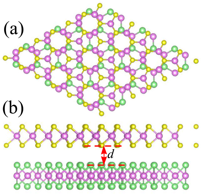
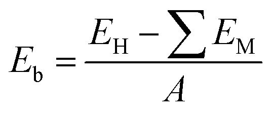
The atomic structures of the MoTe2/MoS2 heterostructure are illustrated in Fig. 2. The MoTe2/MoS2 heterostructure is designed by using (2 × 2) unit cells of a MoS2 monolayer and 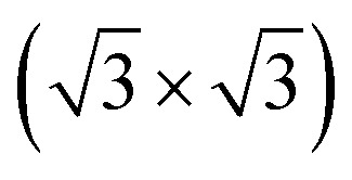 unit cells of a MoTe2 monolayer. The lattice mismatch is calculated to be 2.1%, which is small and can be considered negligible. After geometric optimization, the interlayer spacing d between the two constituent MoTe2 and MoS2 monolayers is obtained to be 3.33 Å. This interlayer spacing is consistent with that in other typical vdW heterostructures51–53 and the experimental value.42 This indicates that the MoTe2/MoS2 heterostructure is characterized by weak vdW interactions. Furthermore, to examine the stability of the MoTe2/MoS2 heterostructure, we calculate the binding energy as follows:
 |
1 |
Here, EH and EM are the total energies of the MoTe2/MoS2 heterostructure and isolated MoX2 (X = S, Te) monolayers, respectively. A stands for the surface area of the heterostructure. The Eb of the MoTe2/MoS2 heterostructure is obtained to be −32.23 meV Å−2. The negative value of the binding energy indicates that the MoTe2/MoS2 heterostructure is structurally stable. In addition, we find that the value of the binding energy is consistent with that in graphite54 and other vdW-based systems.55,56 All these findings confirm that the weak vdW interactions are mainly dominated at the interface of the MoTe2/MoS2 heterostructure. It is noteworthy that the weak vdW interactions keep the MoTe2/MoS2 heterostructure stable and can be synthesized in recent experiments by the transfer method42 or chemical vapor deposition (CVD) method.40
Fig. 2. (a) Top view and (b) side view of the atomic structure of the MoTe2/MoS2 heterostructure.
Furthermore, to check the thermal and mechanical stability of the MoTe2/MoS2 heterostructure, we perform Ab initio molecular dynamics (AIMD) simulation and elastic constant calculation. The fluctuation in the total energy as a function of time steps of the MoTe2/MoS2 heterostructure is depicted in Fig. 3(a). It is evident that the change in the total energy of the MoTe2/MoS2 heterostructure before and after heating for 6 ps is small. Additionally, there is no distortion in the atomic structure of the MoTe2/MoS2 heterostructure after heating for 6 ps. All these findings confirm that the MoTe2/MoS2 heterostructure is thermally stable at room temperature of 300 K. The elastic constants Cij of the MoTe2/MoS2 heterostructure are also calculated to evaluate its mechanical stability. The elastic constants of the MoTe2/MoS2 heterostructure are depicted in Fig. 3(b). The elastic constants of the constituent MoTe2 and MoS2 monolayers are also calculated for comparison. The calculated C11, C12 and C66 of the MoTe2/MoS2 heterostructure are 264.18, 49.17 and 107.50 N m−1, respectively. One can find that these values of the elastic constants satisfy the Born-Huang criteria,57 confirming that the heterostructure is mechanically stable. Furthermore, it is evident that the elastic constants of the MoTe2/MoS2 heterostructure exhibit a substantial enhancement compared to those in the constituent monolayers. Besides, the Young's modulus of the MoTe2/MoS2 heterostructure is also greater than that of the MoTe2 and MoS2 monolayers, exhibiting that the construction of the MoTe2/MoS2 heterostructure leads to an enhancement in the in-plane stiffness, as depicted in Fig. 3(c).
Fig. 3. (a) The fluctuation in the total energy as a function of time steps of the MoTe2/MoS2 heterostructure. The insets show the atomic structures of the MoTe2/MoS2 heterostructure before and after heating for 6 ps. (b) Elastic constants and (c) angle-dependent Young's modulus of the MoTe2/MoS2 heterostructure and the isolated MoTe2 and MoS2 constituent monolayers.
The projected band structure of the MoTe2/MoS2 heterostructure is depicted in Fig. 4(a). The MoTe2/MoS2 heterostructure possesses a semiconducting behavior with an indirect band gap. The VBM is located at the Γ point, whereas the CBM is at the K point. The band gap of the MoTe2/MoS2 heterostructure is 0.97 eV. Such a band gap is still smaller than that of both the constituent MoTe2 and MoS2 monolayers. This implies that the formation of the MoTe2/MoS2 heterostructure gives rise to a reduction in the band gap. A narrower band gap corresponds to stronger optical absorption. Therefore, the construction of the MoTe2/MoS2 heterostructure could lead to an enhancement in the optical properties. More interestingly, the band edges of the MoTe2/MoS2 heterostructure are contributed by distinct layers. The VBM is mainly contributed by the MoTe2 layer, while the CBM comes from the MoS2 layer. This finding suggests that the MoTe2/MoS2 heterostructure forms a type II band alignment. The formation of a type II band alignment was also observed in previous experiments.41,42 Therefore, the type II MoTe2/MoS2 heterostructure can be considered as a promising candidate for the design of optoelectronic and electronic devices, such as photodetectors and transistors.
Fig. 4. (a) Projected band structure, (b) planar-averaged charge density difference and (c) electrostatic potential of the MoTe2/MoS2 heterostructure. Red and blue balls stand for the contributions of the MoS2 and MoTe2 layers, respectively. The dark blue and dark orange represent the charge accumulation and depletion, respectively.
We further consider the charge redistribution at the interface of the MoTe2/MoS2 heterostructure by analyzing the charge density difference (CDD) as follows:
 |
2 |
Here, ρH and ρM are the charge densities of the MoTe2/MoS2 heterostructure and isolated MoX2 (X = S, Se) monolayers, respectively. The planar-averaged CDD of the MoTe2/MoS2 heterostructure is depicted in Fig. 4(b). The dark blue and dark orange regions represent charge accumulation and depletion, respectively. It is evident that the charges are mainly accumulated in the MoTe2 layer and depleted in the MoS2 layer. It indicates that the MoTe2 gains electrons, while the MoS2 layer loses electrons. The electrons flow from the MoS2 to the MoTe2 layer, whereas the holes are transferred in the opposite direction, i.e. from the MoTe2 to the MoS2 layer. Bader charge analysis indicates that there is a small amount of charge transfer of about 10−3 electrons between the two constituent layers. Furthermore, to confirm the charge transfers in the MoTe2/MoS2 heterostructure, we also calculate the work functions of the MoTe2/MoS2 heterostructure and the constituent MoX2 monolayers. The work function of a material can be calculated as: Φ = Evac − EF, where Evac and EF represent the vacuum energy and Fermi energy, respectively. The work functions of the MoTe2 and MoS2 monolayers are calculated to be 4.76 eV and 4.08 eV, respectively. The lower work function of the MoS2 monolayer compared to that of the MoTe2 monolayer confirms that the electrons move from the MoS2 to the MoTe2 layer upon the formation of the heterostructure. The work function of the MoTe2/MoS2 heterostructure is calculated to be 4.98 eV, which is larger than that of the MoS2 and MoTe2 layers. The electrostatic potential of the MoTe2/MoS2 heterostructure is displayed in Fig. 4(c). One can find that the difference in the potential of the MoS2 and MoTe2 layers is small, verifying a small amount of charge transfer between the two layers. In addition, the potential of the MoS2 layer is deeper than that of the MoTe2 layer, confirming that the electrons move from the MoS2 to the MoTe2 layer. Such charge transfer leads to the formation of a built-in electric field, pointing from the MoS2 to the MoTe2 layer in their combined heterostructure.
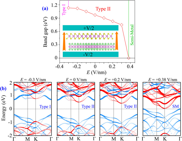
Furthermore, we examine how the external conditions impact the electronic properties and contact types of the MoTe2/MoS2 heterostructure. Therefore, external electric fields and biaxial strains are applied to the heterostructure. The electric fields are applied along the z direction of the heterostructure, as depicted in the inset of Fig. 5(a). The positive direction of the electric fields is defined as from the MoTe2 to the MoS2 layer in their combined heterostructure. It is evident that an electric field can be used to modify the band gaps and change the contact types in the MoTe2/MoS2 heterostructure, as shown in Fig. 5(a). The band gap of the MoTe2/MoS2 heterostructure increases with applying a negative electric field and decreases with applying a positive electric field. The physical mechanism of such change can be described as follows: the direction of the built-in electric field is opposite to that of the negative electric field. Thus, the negative electric field can give rise to an enhancement in the band gap of the MoTe2/MoS2 heterostructure because the total electric field is weakened. On the other hand, the direction of the built-in electric field and positive electric field is the same. The total electric field is strengthened. Thus, the positive electric field causes a reduction in the band gap of the MoTe2/MoS2 heterostructure. The negative electric field can also lead to the transition from type II to type I band alignment, while the positive electric field gives rise to the semiconductor to semimetal transition. The underlying mechanism of these transitions can be described by analyzing the projected band structures of the MoTe2/MoS2 heterostructure under electric fields of different strengths, as depicted in Fig. 5(b). At a critical strength of the negative electric field of −0.3 V nm−1, the CBM of the MoTe2/MoS2 heterostructure is located at the Γ point, as shown in Fig. 5(b). Such a CBM is contributed by the MoTe2 layer, indicating that the negative electric field gives rise to a shift in the CBM of the MoTe2/MoS2 heterostructure from the MoS2 to the MoTe2 layer. Meanwhile, the VBM of the MoTe2/MoS2 heterostructure remains at the Γ point and is contributed by the MoTe2 layer. These findings predict that the MoTe2/MoS2 heterostructure changes to form a type I band alignment. In addition, when a positive electric field is applied, both the CBM and VBM of the MoTe2/MoS2 heterostructure move towards the Fermi level, leading to a reduction in the band gap. At a critical strength of the positive electric field of +0.38 V nm−1, a transition from semiconductor to semimetal can be achieved in the MoTe2/MoS2 heterostructure, as its VBM crosses the Fermi level. Furthermore, it should be mentioned that a high strength electric field can be generated from the tabletop terahertz source within an electrolyte top gate.58 Additionally, a high strength electric field always requires high-k and a back (top)-gated device architecture.59 All these findings prove that the electric field can be considered as an effective tool to manipulate the electronic properties and contact type of the MoTe2/MoS2 heterostructure, thereby expanding its potential applications in electronics and optoelectronics.60
Fig. 5. (a) The variation of the band gaps and (b) the projected band structures of the MoTe2/MoS2 heterostructure under electric fields of different strengths. The inset shows the schematic model of applied electric fields along the z direction of the heterostructure.
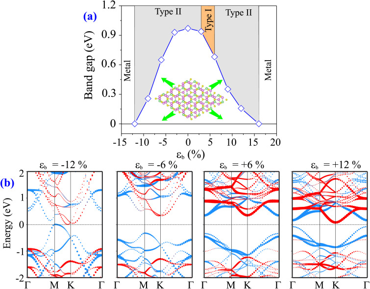
The biaxial in-plane strain is derived from εb = (a − a0)/a0 × 100%, where a and a0 are the lattice parameters of the MoTe2/MoS2 heterostructure with and without the application of the biaxial strain, respectively. The negative and positive values refer to the compressive and tensile strains, respectively. The schematic model of the in-plane biaxial strain is depicted in the inset of Fig. 6. It is obvious that the strain causes a change in both the band gap values and contact types of the MoTe2/MoS2 heterostructure. The biaxial strain gives rise to a reduction in the band gap of the MoTe2/MoS2 heterostructure, as depicted in Fig. 6(a). The band gap of the MoTe2/MoS2 heterostructure can be reduced down to zero under the application of either a compressive strain of −12% or a tensile strain of +16%. This observation indicates that the transition from semiconductor to metal can be achieved in the MoTe2/MoS2 heterostructure under the application of biaxial strain. Additionally, the tensile strain can also lead to the transformation between type II and type I band alignment in the MoTe2/MoS2 heterostructure.
Fig. 6. (a) The variation of the band gaps and (b) the projected band structures of the MoTe2/MoS2 heterostructure under different ratios of strain. The inset shows the schematic model of the applied in-plane biaxial strain to the heterostructure.
To have a better understanding of the impact of the strain, we further analyze the projected band structures of the MoTe2/MoS2 heterostructure under different strain ratios, as illustrated in Fig. 6(b). When the compressive strain is applied, both the VBM and CBM of the MoTe2/MoS2 heterostructure shift towards the Fermi level, giving rise to a reduction in the band gap values. Similarly, the band edges of both the MoTe2 and MoS2 layers in the MoTe2/MoS2 heterostructure move closer to the Fermi level under the tensile strain. Under a tensile strain of εb = +3%, the CBM of the MoTe2/MoS2 heterostructure shifts from the K to the Γ point. Thus, the indirect-to-direct transition is achieved in the MoTe2/MoS2 heterostructure. In addition, both the VBM and CBM of the MoTe2/MoS2 heterostructure now come from the MoTe2 layer, indicating that there occurs a transition from type II to type I band alignment. The type I band alignment is maintained in the MoTe2/MoS2 heterostructure under tensile strains ranging from +3% to +6%. When the tensile strain is larger than +6%, the CBM of the MoTe2/MoS2 heterostructure is recovered from the Γ to the K point, while the VBM is preserved at the Γ point. This recovery indicates that there is a transition from direct to indirect semiconductor and a conversion from type I to type II band alignment because the band edges of the MoTe2/MoS2 heterostructure are contributed by the MoTe2 layer. When the tensile strain is larger than 16%, the band edges of the MoTe2/MoS2 heterostructure cross the Fermi level, leading to a transition from semiconductor to metal. Our findings prove that the in-plane biaxial strain can effectively be used to tailor the electronic properties and contact types in the MoTe2/MoS2 heterostructure, thereby expanding its potential applications in multifunctional devices.
4. Conclusions
In conclusion, we have performed first-principles calculations to design a 2D vdW MoTe2/MoS2 heterostructure with the formation of a type II band alignment. Our results indicate that the MoTe2/MoS2 heterostructure is structurally, thermally and mechanically stable. The weak vdW interactions are found to be dominated at the interface of the MoTe2/MoS2 heterostructure and thus it can be synthesized in recent experiments by the transfer method or chemical vapor deposition. The vdW MoTe2/MoS2 heterostructure exhibits a staggered type II band alignment, effectively separating the electrons and holes at the interface and thereby extending the carrier lifetime. Furthermore, our findings reveal that the electronic properties and contact types of type II vdW MoTe2/MoS2 heterostructures can be tailored under the application of external conditions, including an electric field and in-plane biaxial strain. The semiconductor–semimetal–metal transition and type II–type I conversion can be achieved in the vdW MoTe2/MoS2 heterostructure. Our findings underscore the potential of the vdW MoTe2/MoS2 heterostructure for the design and fabrication of multifunctional applications, including electronics and optoelectronics.
Conflicts of interest
There are no conflicts to declare.
Acknowledgments
This research is funded by the Vietnam Ministry of Education and Training under Grant No. B2023.DNA.06.
References
- Novoselov K. S. Geim A. K. Morozov S. V. Jiang D.-e. Zhang Y. Dubonos S. V. Grigorieva I. V. Firsov A. A. Science. 2004;306:666–669. doi: 10.1126/science.1102896. [DOI] [PubMed] [Google Scholar]
- Sarkar A. S. Stratakis E. Adv. Sci. 2020;7:2001655. doi: 10.1002/advs.202001655. [DOI] [PMC free article] [PubMed] [Google Scholar]
- Yu M. Hilse M. Zhang Q. Liu Y. Wang Z. Law S. ACS Appl. Nano Mater. 2024 doi: 10.1021/acsanm.3c05984. [DOI] [Google Scholar]
- Manzeli S. Ovchinnikov D. Pasquier D. Yazyev O. V. Kis A. Nat. Rev. Mater. 2017;2:1–15. [Google Scholar]
- Yang R. Fan Y. Zhang Y. Mei L. Zhu R. Qin J. Hu J. Chen Z. Hau Ng Y. Voiry D. et al. . Angew. Chem., Int. Ed. 2023;62:e202218016. doi: 10.1002/anie.202218016. [DOI] [PubMed] [Google Scholar]
- Wang Y. Guo T. Tian Z. Bibi K. Zhang Y.-Z. Alshareef H. N. Adv. Mater. 2022;34:2108560. doi: 10.1002/adma.202108560. [DOI] [PubMed] [Google Scholar]
- Gogotsi Y. and Anasori B., The Rise of MXenes, 2019 [DOI] [PubMed] [Google Scholar]
- Gogotsi Y., The Future of MXenes, 2023 [Google Scholar]
- Wang Y. Liu L. Ma T. Zhang Y. Huang H. Adv. Funct. Mater. 2021;31:2102540. doi: 10.1002/adfm.202102540. [DOI] [Google Scholar]
- Rono N. Kibet J. K. Martincigh B. S. Nyamori V. O. Crit. Rev. Solid State Mater. Sci. 2021;46:189–217. doi: 10.1080/10408436.2019.1709414. [DOI] [Google Scholar]
- Jiang L. Yuan X. Pan Y. Liang J. Zeng G. Wu Z. Wang H. Appl. Catal., B. 2017;217:388–406. doi: 10.1016/j.apcatb.2017.06.003. [DOI] [Google Scholar]
- Kim J. Lee Y. Kang M. Hu L. Zhao S. Ahn J.-H. Adv. Mater. 2021;33:2005858. doi: 10.1002/adma.202005858. [DOI] [PubMed] [Google Scholar]
- Liu X. Hersam M. C. Nat. Rev. Mater. 2019;4:669–684. doi: 10.1038/s41578-019-0136-x. [DOI] [Google Scholar]
- De Leon N. P. Itoh K. M. Kim D. Mehta K. K. Northup T. E. Paik H. Palmer B. Samarth N. Sangtawesin S. Steuerman D. W. Science. 2021;372:eabb2823. doi: 10.1126/science.abb2823. [DOI] [PubMed] [Google Scholar]
- Huh W. Lee D. Lee C.-H. Adv. Mater. 2020;32:2002092. doi: 10.1002/adma.202002092. [DOI] [PubMed] [Google Scholar]
- Geim A. K. Grigorieva I. V. Nature. 2013;499:419–425. doi: 10.1038/nature12385. [DOI] [PubMed] [Google Scholar]
- Liu Y. Weiss N. O. Duan X. Cheng H.-C. Huang Y. Duan X. Nat. Rev. Mater. 2016;1:1–17. [Google Scholar]
- Novoselov K. Mishchenko A. Carvalho A. Castro Neto A. Science. 2016;353:aac9439. doi: 10.1126/science.aac9439. [DOI] [PubMed] [Google Scholar]
- Liang S.-J. Cheng B. Cui X. Miao F. Adv. Mater. 2020;32:1903800. doi: 10.1002/adma.201903800. [DOI] [PubMed] [Google Scholar]
- Cheng R. Wang F. Yin L. Wang Z. Wen Y. Shifa T. A. He J. Nat. Electron. 2018;1:356–361. doi: 10.1038/s41928-018-0086-0. [DOI] [Google Scholar]
- Kim J. Rhee D. Song O. Kim M. Kwon Y. H. Lim D. U. Kim I. S. Mazánek V. Valdman L. Sofer Z. et al. . Adv. Mater. 2022;34:2106110. doi: 10.1002/adma.202106110. [DOI] [PubMed] [Google Scholar]
- Li J. Yang X. Liu Y. Huang B. Wu R. Zhang Z. Zhao B. Ma H. Dang W. Wei Z. et al. . Nature. 2020;579:368–374. doi: 10.1038/s41586-020-2098-y. [DOI] [PubMed] [Google Scholar]
- Selamneni V. Sahatiya P. Microelectron. Eng. 2023;269:111926. doi: 10.1016/j.mee.2022.111926. [DOI] [Google Scholar]
- Nasrin K. Sudharshan V. Subramani K. Sathish M. Adv. Funct. Mater. 2022;32:2110267. doi: 10.1002/adfm.202110267. [DOI] [Google Scholar]
- Liu F. Jin S. Xia Q. Zhou A. Fan L.-Z. J. Energy Chem. 2021;62:220–242. doi: 10.1016/j.jechem.2021.03.017. [DOI] [Google Scholar]
- Yin Y. Gong Q. Yi M. Guo W. Adv. Funct. Mater. 2023;33:2214050. doi: 10.1002/adfm.202214050. [DOI] [Google Scholar]
- Tho C. C. Guo S.-D. Liang S.-J. Ong W. L. Lau C. S. Cao L. Wang G. Ang Y. S. Appl. Phys. Rev. 2023;10:041307. [Google Scholar]
- Padilha J. E. Fazzio A. da Silva A. J. Phys. Rev. Lett. 2015;114:066803. doi: 10.1103/PhysRevLett.114.066803. [DOI] [PubMed] [Google Scholar]
- Batmunkh M. Bat-Erdene M. Shapter J. G. Adv. Mater. 2016;28:8586–8617. doi: 10.1002/adma.201602254. [DOI] [PubMed] [Google Scholar]
- Ren K. Sun M. Luo Y. Wang S. Yu J. Tang W. Appl. Surf. Sci. 2019;476:70–75. doi: 10.1016/j.apsusc.2019.01.005. [DOI] [Google Scholar]
- Chiu M.-H. Zhang C. Shiu H.-W. Chuu C.-P. Chen C.-H. Chang C.-Y. S. Chen C.-H. Chou M.-Y. Shih C.-K. Li L.-J. Nat. Commun. 2015;6:7666. doi: 10.1038/ncomms8666. [DOI] [PMC free article] [PubMed] [Google Scholar]
- Yu J. H. Lee H. R. Hong S. S. Kong D. Lee H.-W. Wang H. Xiong F. Wang S. Cui Y. Nano Lett. 2015;15:1031–1035. doi: 10.1021/nl503897h. [DOI] [PubMed] [Google Scholar]
- Son M. Jang H. Seo D.-B. Lee J. H. Kim J. Kim M. Kang S. Yim S. Song W. Yoo J.-W. et al. . Adv. Funct. Mater. 2024;34:2308906. doi: 10.1002/adfm.202308906. [DOI] [Google Scholar]
- Xue Y. Zhang Y. Liu Y. Liu H. Song J. Sophia J. Liu J. Xu Z. Xu Q. Wang Z. et al. . ACS Nano. 2016;10:573–580. doi: 10.1021/acsnano.5b05596. [DOI] [PubMed] [Google Scholar]
- Ahn J. Kyhm J.-H. Kang H. K. Kwon N. Kim H.-K. Park S. Hwang D. K. ACS Photonics. 2021;8:2650–2658. doi: 10.1021/acsphotonics.1c00598. [DOI] [Google Scholar]
- Huang M. Li S. Zhang Z. Xiong X. Li X. Wu Y. Nat. Nanotechnol. 2017;12:1148–1154. doi: 10.1038/nnano.2017.208. [DOI] [PubMed] [Google Scholar]
- Huang Y. Pan Y.-H. Yang R. Bao L.-H. Meng L. Luo H.-L. Cai Y.-Q. Liu G.-D. Zhao W.-J. Zhou Z. et al. . Nat. Commun. 2020;11:2453. doi: 10.1038/s41467-020-16266-w. [DOI] [PMC free article] [PubMed] [Google Scholar]
- Kim H. G. Lee H.-B.-R. Chem. Mater. 2017;29:3809–3826. doi: 10.1021/acs.chemmater.6b05103. [DOI] [Google Scholar]
- Cai Z. Liu B. Zou X. Cheng H.-M. Chem. Rev. 2018;118:6091–6133. doi: 10.1021/acs.chemrev.7b00536. [DOI] [PubMed] [Google Scholar]
- Ding Y. Zhou N. Gan L. Yan X. Wu R. Abidi I. H. Waleed A. Pan J. Ou X. Zhang Q. et al. . Nano Energy. 2018;49:200–208. doi: 10.1016/j.nanoen.2018.04.055. [DOI] [Google Scholar]
- Ji X. Bai Z. Luo F. Zhu M. Guo C. Zhu Z. Qin S. ACS Omega. 2022;7:10049–10055. doi: 10.1021/acsomega.1c06009. [DOI] [PMC free article] [PubMed] [Google Scholar]
- Chen Y. Wang X. Wu G. Wang Z. Fang H. Lin T. Sun S. Shen H. Hu W. Wang J. et al. . Small. 2018;14:1703293. doi: 10.1002/smll.201703293. [DOI] [PubMed] [Google Scholar]
- Pezeshki A. Shokouh S. H. H. Nazari T. Oh K. Im S. Adv. Mater. 2016;28:3216–3222. doi: 10.1002/adma.201504090. [DOI] [PubMed] [Google Scholar]
- Giannozzi P. Baroni S. Bonini N. Calandra M. Car R. Cavazzoni C. Ceresoli D. Chiarotti G. L. Cococcioni M. Dabo I. et al. . J. Phys.: Condens.Matter. 2009;21:395502. doi: 10.1088/0953-8984/21/39/395502. [DOI] [PubMed] [Google Scholar]
- Giannozzi P. Andreussi O. Brumme T. Bunau O. Nardelli M. B. Calandra M. Car R. Cavazzoni C. Ceresoli D. Cococcioni M. et al. . J. Phys.: Condens.Matter. 2017;29:465901. doi: 10.1088/1361-648X/aa8f79. [DOI] [PubMed] [Google Scholar]
- Perdew J. P. Burke K. Ernzerhof M. Phys. Rev. Lett. 1998;80:891. doi: 10.1103/PhysRevLett.80.891. [DOI] [PubMed] [Google Scholar]
- Kresse G. Joubert D. Phys. Rev. B: Condens. Matter Mater. Phys. 1999;59:1758. doi: 10.1103/PhysRevB.59.1758. [DOI] [Google Scholar]
- Heyd J. Scuseria G. E. Ernzerhof M. J. Chem. Phys. 2003;118:8207–8215. doi: 10.1063/1.1564060. [DOI] [Google Scholar]
- Grimme S. Antony J. Ehrlich S. Krieg H. J. Chem. Phys. 2010;132:154104. doi: 10.1063/1.3382344. [DOI] [PubMed] [Google Scholar]
- Wilson J. A. Yoffe A. Adv. Phys. 1969;18:193–335. doi: 10.1080/00018736900101307. [DOI] [Google Scholar]
- Tang K. Qi W. Li Y. Wang T. J. Phys. Chem. C. 2018;122:7027–7032. doi: 10.1021/acs.jpcc.8b01476. [DOI] [Google Scholar]
- Shu H. Zhao M. Sun M. ACS Appl. Nano Mater. 2019;2:6482–6491. doi: 10.1021/acsanm.9b01422. [DOI] [Google Scholar]
- Luo Y. Ren K. Wang S. Chou J.-P. Yu J. Sun Z. Sun M. J. Phys. Chem. C. 2019;123:22742–22751. doi: 10.1021/acs.jpcc.9b05581. [DOI] [Google Scholar]
- Liu Z. Liu J. Z. Cheng Y. Li Z. Wang L. Zheng Q. Phys. Rev. B. 2012;85:205418. doi: 10.1103/PhysRevB.85.205418. [DOI] [Google Scholar]
- Girifalco L. A. Hodak M. Phys. Rev. B: Condens. Matter Mater. Phys. 2002;65:125404. doi: 10.1103/PhysRevB.65.125404. [DOI] [Google Scholar]
- Wang J. Bai L. Zhao X. Chen C. Niu L. Phys. E. 2023;149:115668. doi: 10.1016/j.physe.2023.115668. [DOI] [Google Scholar]
- Mouhat F. Coudert F.-X. Phys. Rev. B: Condens. Matter Mater. Phys. 2014;90:224104. doi: 10.1103/PhysRevB.90.224104. [DOI] [Google Scholar]
- Vicario C. Monoszlai B. Hauri C. P. Phys. Rev. Lett. 2014;112:213901. doi: 10.1103/PhysRevLett.112.213901. [DOI] [Google Scholar]
- Robertson J. Eur. Phys. J.: Appl. Phys. 2004;28:265–291. doi: 10.1051/epjap:2004206. [DOI] [Google Scholar]
- Tan C. W. Xu L. Er C. C. Chai S.-P. Kozinsky B. Yang H. Y. Yang S. A. Lu J. Ang Y. S. Adv. Funct. Mater. 2024;34:2308679. doi: 10.1002/adfm.202308679. [DOI] [Google Scholar]


