

Abstract
Controlling heat flow is a key challenge for applications ranging from thermal management in electronics to energy systems, industrial processing, and thermal therapy. However, progress has generally been limited by slow response times and low tunability in thermal conductance. In this work, we demonstrate an electronically gated solid-state thermal switch using self-assembled molecular junctions to achieve excellent performance at room temperature. In this three-terminal device, heat flow is continuously and reversibly modulated by an electric field through carefully controlled chemical bonding and charge distributions within the molecular interface. The devices have ultrahigh switching speeds above 1 megahertz, have on/off ratios in thermal conductance greater than 1300%, and can be switched more than 1 million times. We anticipate that these advances will generate opportunities in molecular engineering for thermal management systems and thermal circuit design.
Mastering electricity has driven the current age of modern information technology. For electronic devices, as early as the 1920s, scientists understood how to make a two-terminal device by contacting a sharp metal tip and a semiconductor crystal. These point-contact diodes have a large contrast in resistance depending on the flow direction of current and were used to rectify signals and make simple AM radio receivers. However, it took many years before the three-terminal solid-state device—the transistor—was invented at Bell Laboratories in 1947 (1). In the concept of electronics, the conductance can be continuously tuned by applying voltage through a third terminal. This breakthrough was recognized by the Nobel Prize in Physics in 1956 (2) and became a cornerstone of modern electronics, greatly influencing everyday life ever since.
For thermal devices, much work has been devoted to the control of heat flow for wide-spread applications ranging from thermal management in electronics to heating and cooling facilities in households and industry, thermal energy conversion and storage, and vehicle and aerospace operations (3–10). However, such control over heat is far behind the degree of control that has been achieved for electrons. Fundamentally, controlling thermal conductance using convenient handles—e.g., electric fields—has been a long-term but elusive dream for physicists and engineers, challenged by the spectral distribution of heat carriers and their complicated and weak interactions with external fields (11).
Advances in nanotechnology have greatly extended our understanding of and capabilities in the design and control of materials’ properties and have provided opportunities for thermal control. For example, heat transport at low dimensions can be anomalous and can break Fourier’s law. Early progress in demonstrating thermal rectification has been reported using carbon and boron nitride nanotubes with inhomogeneous mass loading (12). In such two-terminal devices, thermal conductance switching changes of up to 7% were observed for reversed heating directions. A great deal of theoretical and experimental work has been developed (13–20) to tune room-temperature thermal transport in solids relying mainly on structural phase changes or mass transfer, electrochemical scattering motion of ions, or other heat carriers. The usefulness of these approaches is largely limited not only by small switching ratios but also by intrinsically slow response speeds—typically from minutes to hours (i.e., usually far below 1 Hz). In this work, we demonstrate electrically gated three-terminal thermal switches that achieve high performance with >1-MHz switching speed, 1300% tunability in thermal conductance, and high reversibility over 1 million switching cycles. These values are substantial advancements over current solid-state thermal devices at room temperature.
Electrically gated three-terminal thermal devices
We illustrate the concept of our thermal switch with a symbolic diagram in Fig. 1A that is analogous to an electronic transistor. The device channel is contacted between a hot and cold thermal reservoir, with temperatures TH and TC, respectively. A third terminal using an electric field serves as the gate to control thermal conductance of the channel and thereby the heat flow. We designed this thermal switch and imaged the microstructure of our fabricated device [see supplementary materials (21) for details] with scanning electron microscopy (SEM) (Fig. 1B) from a tilted top-view angle and used high-resolution transmission electron microscopy (TEM) from a cross-sectional angle (Fig. 1C). We show a thin-film structure with an atomically resolved interface. This multilayer solid-state thin film consists of a self-assembled monolayer (SAM) of carboranethiol cage molecules on a bottom layer of gold (Au) from evaporative deposition and topped by single-layer graphene, which serves as the active conduction channel. Specifically, we achieved a cross-plane molecular junction using a SAM based on 9-SH-o-C2B10H11 (O9) (22–24). These molecules form high-quality monolayers with minimum defect structures in complete monolayers limited to translational and rotational offsets in the registry of attachment to the substrate. We have shown that such layers provide the capability to tune the band alignment between contacts and the active layers in organic electronics (24). In this work, we show a typical scanning tunneling microscopy image of the carboranethiolate SAM and its closely packed and uniform structure with an atomically smooth exposed surface (Fig. 1D). The mechanism of the thermal switching is based on electrical control of atomic bond strengths for the molecular junctions that thereby controls thermal conductance.
Fig. 1. Device design and transport performance of the molecular thermal switches.

(A) Conceptual illustration of the three-terminal thermal device. (B) Tilted top-view SEM image of the microstructure, consisting of a monolayer of carboranethiol cage molecules on a Au layer topped by single-layer graphene. (C) High-resolution cross-sectional TEM image of the device structure showing the atomically resolved interface. (D) Scanning tunneling microscopy image of the carboranethiolate molecular monolayer on Au{111}. The image was acquired in constant-current mode at a −0.1-V bias under ambient conditions. (E) The measured thermal conductance () as a function of gate voltage (). Red and blue curves represent device structures with and without graphene, respectively, as illustrated by the inset schematics. The shadowed background represents measurement uncertainty. (F) Reversibility test of electrical gating between ± 2.5 V on cycling measurements of the thermal device with graphene up to 1 million times. Red and black dashed guidelines indicate ratios of 1300% and 100%, respectively. The value of is 10 MW/m2K.
We measured the thermal conductance (G) of the device per unit area, which shows a strong dependence of gate voltage () when applied across the molecular junction (Fig. 1E). When is applied from 2.5 to −2.5 V, G exhibits a large monotonic increase from 10 to 134 MW/m2K (red symbols). The thermal conductance control is >1300%, much higher than that of other demonstrations of electrical modulation (15, 16). We also investigated molecular junctions where graphene was removed, and the G shows ambipolar behavior (blue symbols) that increases from 23 MW/m2K when to 84 MW/m2K when and then decreases to 8.0 MW/m2K when . To test device reversibility, we performed the gate switching measurement for up to 1 million cycles. Our cycling measurements indicate that the gate switching on thermal conductance is highly reversible between the on and off states (Fig. 1F). This dynamic and reversible tunability of thermal conductance using an electric field effect demonstrates the robustness of these molecular thermal devices with high switching ratios (15, 16).
First-principles theory
To elucidate the fundamental operation mechanisms, we performed first-principles calculations to determine the atomic charge distributions and thus the bonding energy () of the molecular channel. We applied density functional theory (DFT) to calculate the spatial charge distribution over the atomic structure of Au-SAM-graphene (Fig. 2A) (21). Au and the S atoms (inside the SAM) form chemical bonds by sharing electrons, and the bond strength is characterized by the charge density difference (25)
| (1) |
where , and are the charge density distributions of the bonded system, of the isolated Au surface, and of the isolated SAM, respectively. Thus, is responsible for the formation of the Au-SAM bond. To reveal the deterministic effects of on electron sharing, we quantified the redistribution of electrons through the calculation of as a function of electric field.
Fig. 2. Thermal switching operation mechanisms.

(A) Atomic structure of the Au-monolayer(S-carborane)–graphene system. (B and C) Deviational charge density differences () determined by DFT under an electric field of 0.6 V/Å (B) and −0.4 V/Å (C). Insets indicate the three-dimensional charge distributions. (D) Bond energies determined by DFT. Plotted as a function of are the calculation results for the atomic bonds, including Au-S without graphene (blue solid line), Au-S with graphene (blue dashed line), and SAM-graphene (red line). (E and F) Experimental measurements of Raman peaks as a function of . (E) Gate tuning of the stretching vibrational mode for Au-S. (F) Gate tuning of the 2D mode for graphene-SAM. (G and H) Molecular dynamics simulation results of thermal conductance as a function of bond energy for Au-SAM (G) and graphene-SAM (H) systems.
We performed calculations for the Au-SAM system (i.e., without graphene). We illustrate the gating effects by plotting the variations of the charge density distributions () under applied gate voltages (Fig. 2, B and C). The results indicate that the electrons at the bonding site—i.e., the Au-S bonds—have a large dynamic change. Electrons are pulled away from the S atom when a positive is applied (Fig. 2B). By contrast, the electrons are more attracted toward the S atom on the carboranethiolate molecule when a negative is applied (Fig. 2C). In either case, reduction in shared electrons between S and Au atoms eventually suppresses their covalent interactions and weakens their bond strength (26). Quantitatively, we calculated the Au-SAM bond energy () through first-principles theory (21) as a function of electrical voltage
| (2) |
where , and are the energy of the bonded system, that of the isolated Au, and that of the isolated SAM, respectively. Because the Au-SAM bond is one of the weakest covalent bonds in the system (27–29), our calculation shows that gate tuning of is considerable, and the Au-S bond forms the thermal resistance inside the channel. Notably, (blue solid curve) exhibits an ambipolar dependence as a function of voltage (Fig. 2D), similar to the measured trend for thermal conductance (Fig. 1E). Consistently, substantial changes in electrical conductance, hybridization, and presumably charge redistribution were observed at molecule-substrate interfaces as a result of motion (tilt) of adsorbed molecules (30).
We also performed first-principles calculations for a thermal device including the top graphene layer—i.e., the Au-SAM-graphene system. We applied nonlocal DFT to capture such long-range interactions accurately with an ab initio approach (31–34). Using Eq. 2, we determined the bond energy for SAM-graphene (Fig. 2D). We found a monotonic dependence for (red curve) on voltage, which is a similar trend as observed in our measurements of gated thermal conductance. The calculation results are consistent with generally understood van der Waals interaction energies being derived from higher-order dipole-dipole interactions based on quantum perturbation theory (35). The bond energies increase with external electric fields because of the enhanced dipole moments determined by positive and negative charge separation. In addition, our theory shows strengthened Au-SAM bonding and its weak voltage dependence after adding a graphene layer (Fig. 2D, blue dashed line) because of the redistribution of charge density (21) at these interfaces (36). Therefore, our first-principles calculations indicate a fundamental tuning mechanism for thermal conductance by electric field–modulated charge redistribution. This family of carborane molecules are particularly well suited for this purpose, not only because of their robust self-assembly but because charge distribution within the cage is determined by the carborane cage selected as well as the point or points of attachment (22, 37). We anticipate the potential for further enhancement of these devices by optimizing the polarizability and charge distributions of the molecular layer by selecting both the molecular isomers of the cage molecules and the chemistries of attachment.
In situ vibrational spectroscopy
To test the calculated results, we experimentally measured the vibrational spectra corresponding to the interface bonding using in situ surface-enhanced Raman as a function of gate voltage. We applied the excitation laser with parallel incidence to the cross-plane of the thermal device film to study the interface vibrational modes. The A1 and 2D Raman peaks are located at ~296 and 2608 cm−1, respectively. The A1 mode is the symmetric Au-S stretching vibration of Au-carboranethiolate (Fig. 2E) (38). As shown in the two-dimensional scanning image (Fig. 2E), with sweeping from +2 to −2 V, the Raman peak first increases from 276.2 to 294.0 cm−1 and then decreases to 274.9 cm−1. We observe ambipolar behavior consistent with the theoretically predicted bond energy variations (Fig. 2D) (39) and the observed ambipolar behavior of the measured conductance. For the Au-SAM-graphene system, we measured the evolution of the 2D mode Raman spectra as a function of (Fig. 2F). The 2D Raman peak represents the double resonance process of photon scattering with two transverse optical (TO) phonons near the Brillouin edge and has a robust vibrational footprint frequency that quantifies the strain-dependent shift resulting from the spatial force heterogeneity. In this case, because of the curvature of the carborane molecules, the repulsive and attractive forces at the apex and shoulder of carborane stretch the graphene and induce lateral strains on the graphene through van der Waals interactions (40). Thus, stronger van der Waals interactions result in larger 2D Raman peak position shifts (41). The 2D Raman peak shows monotonic decreases from 2612.4 to 2599.1 cm−1 (a shift of 13.3 cm−1) when the gate voltage is swept from +2 to −2V (Fig. 2F), which indicates continuous and tunable modulation through van der Waals interactions under the applied electric field. The correlations between the van der Waals interactions and strain can be evaluated further from our measurements. The biaxial strain of graphene caused by the van der Waals interactions can be estimated from Fig. 2F to be ~0.08%, according to the 2D Raman peak shift coefficient of ~160 cm−1/% versus biaxial strain in the linear elasticity regime (41). Because the strain is induced by the van der Waals interactions, the change of the interface bond energy can be estimated from the mechanical energy change. Considering a harmonic model for graphene with a stiffness of 150 N/m (42), the Raman peak shift estimates such energy changes as ~0.35 eV per molecule, which agrees with the predicted value from our DFT calculations (Fig. 2D). These in situ Raman measurements are consistent with electric field–induced changes in bond energy, predicted by our first-principles theory, as the dynamic tuning mechanism for the thermal switching behaviors. In addition, we simulated the thermal conductance to evaluate its dependence on bond energies using molecular dynamics (43). Our first principles–derived bond energies were input into the simulations to describe the interface interactions. The simulation domain mimics the experimental conditions without and with graphene (Fig. 2, G and H, respectively) under the varied bond energy for and , which verifies the trend of gate tuning on thermal conductance.
High-speed thermal switching
As a further step, we performed direct measurements to characterize the thermal switching speeds. A key challenge for developing solid-state thermal switches is the intrinsically slow motion of heat and/or mass flow that usually limits thermal switching responses to minutes orhours. In this molecular thermal switch design, however, the driving mechanisms are field-induced, nearly instantaneous atomic-level charge and bonding dynamics, with the result that we achieved ultrahigh switching frequencies. We tested gating frequency using ultrafast optical spectroscopy based on the time-domain thermoreflectance (TDTR) technique. This technique is well suited for measuring the molecular switches because no physical contact is required with the sample, and the measurement provides high measurement resolution and accuracy. We have used TDTR to measure the thermal conductance of a wide range of materials, including molecular junctions (4, 9, 17, 43–47). We used a train of 800-nm femtosecond laser pulses divided into a pump beam and a probe beam by a beam splitter (Fig. 3A). We used the pump beam to heat up the devices and the probe beam to detect the resulting temperature responses and determine the thermal conductance. The ultrafast measurements with subpicosecond time resolution enable effectively instantaneous thermal conductance determinations in real time upon gate tuning. To test the switching frequency (), time-dependent conductance changes versus periodically varied gating voltage are monitored. Our measured thermal conductance (circles) is reversibly switched between on and off states, following with frequencies from 0.1 Hz to 1 MHz (Fig. 3B). The close synchronization between the thermal conductance and gating voltage (Fig. 3B) and the two-dimensional frequency scanning plot (Fig. 3C) indicates that the switching speed of our thermal switching is at least 1 MHz.
Fig. 3. High–switching speed measurements of electrically gated molecular thermal switch.
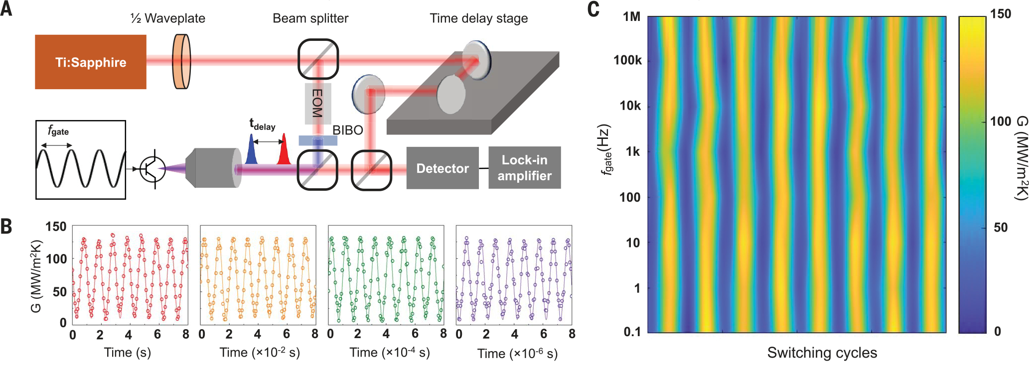
(A) Schematic of experimental setup for time-dependent thermal conductance measurements under periodic gating voltage with varied gating frequency (). BIBO, bismuth triborate; EOM, electro-optic modulator; , time delay. (B) Experimental data of thermal conductance (circles) in response to gate fields with different frequencies (), plotted together with sine function waves of 1 Hz, 100 Hz, 10 kHz, and 1 MHz (solid lines). (C) Two-dimensional plot for thermal switching cycles versus scanning frequency response up to 1 MHz, measured at every decade. Note that 1 MHz is the instrument limit by the thermal detection bandwidth of the measurement setup.
Conclusions
We have developed an electrically gated thermal switch based on solid-state molecular structures that demonstrates excellent performance at room temperature, with switching speeds above 1 MHz, switching ratios greater than 1300%, and high reversibility over 1 million gating cycles. We performed first-principles atomistic calculations and in situ vibrational spectra measurements to capture the dynamic physics of interface bonding and quantitatively explained our experimental results. The cage molecules that we used can be tuned to optimize polarizability and thus charge redistribution under gate control at the overlayer interfaces to enhance switching ratios further. Detailed calculations, as demonstrated above, guide both molecular and device design. With the availability of electrical control over heat flow and compatible fabrication with modern electronics, phonons can be integrated with electronics and photonics for future information processing. We anticipate that this concept will aid in the discovery of new opportunities in the control of thermal current for logic circuits as well as in thermal management and energy technologies.
Supplementary Material
Funding:
Y.H. acknowledges support from the National Institute of General Medical Sciences (NIGMS) under grant no. R35GM147391, the Alfred P. Sloan Research Foundation under grant no. FG-2019-11788, and the National Science Foundation (NSF) under award no. DMR-1753393. P.S.W. acknowledges support from the NSF under grant no. CHE-2004238. We acknowledge support from UCLA Nanolab and California NanoSystems Institute and the computational and storage services associated with the Hoffman 2 Shared Cluster provided by UCLA Institute for Digital Research and Education’s Research Technology Group; from the Bridges-2 at Pittsburgh Supercomputing Center through allocation no. DMR180111 from Extreme Science and Engineering Discovery Environment supported by NSF grant no. 1548562; and from the Advanced Cyberinfrastructure Coordination Ecosystem: Services & Support (ACCESS) program supported by NSF grants no. 2138259, no. 2138286, no. 2138307, no. 2137603, and no. 2138296.
Footnotes
Competing interests: The authors declare no competing interests.
Data and materials availability: All data are available in the main text or the supplementary materials.
REFERENCES AND NOTES
- 1.Bardeen J, Brattain WH, Phys. Rev. 74, 230–231 (1948). [Google Scholar]
- 2.The Nobel Prize in Physics 1956; https://www.nobelprize.org/prizes/physics/1956/summary/.
- 3.“Heating and Cooling” (US Department of Energy); https://www.energy.gov/energysaver/heating-and-cooling.
- 4.Kang JS, Li M, Wu H, Nguyen H, Hu Y, Science 361, 575–578 (2018). [DOI] [PubMed] [Google Scholar]
- 5.Chu S, Majumdar A, Nature 488, 294–303 (2012). [DOI] [PubMed] [Google Scholar]
- 6.Waldrop MM, Nature 530, 144–147 (2016). [DOI] [PubMed] [Google Scholar]
- 7.Ball P, Nature 492, 174–176 (2012). [DOI] [PubMed] [Google Scholar]
- 8.International Technology Roadmap for Semiconductors, ITRS 2.0; www.itrs2.net/.
- 9.Li S et al. , Nature 612, 459–464 (2022). [DOI] [PubMed] [Google Scholar]
- 10.Qin Z, Li M, Flohn J, Hu Y, Chem. Commun. 57, 12236–12253 (2021). [DOI] [PubMed] [Google Scholar]
- 11.Ziman JM, Electrons and Phonons: The Theory of Transport Phenomena in Solids (Oxford Univ. Press, 1960). [Google Scholar]
- 12.Chang CW, Okawa D, Majumdar A, Zettl A, Science 314, 1121–1124 (2006). [DOI] [PubMed] [Google Scholar]
- 13.Li B, Wang L, Casati G, Appl. Phys. Lett. 88, 143501 (2006). [Google Scholar]
- 14.Li N et al. , Rev. Mod. Phys. 84, 1045–1066 (2012). [Google Scholar]
- 15.Wehmeyer G, Yabuki T, Monachon C, Wu J, Dames C, Appl. Phys. Rev. 4, 041304 (2017). [Google Scholar]
- 16.Swoboda T, Klinar K, Yalamarthy AS, Kitanovski A, Munoz Rojo M, Adv. Electron. Mater. 7, 2000625 (2021). [Google Scholar]
- 17.Kang JS, Ke M, Hu Y, Nano Lett. 17, 1431–1438 (2017). [DOI] [PubMed] [Google Scholar]
- 18.Zhu G et al. , Nat. Commun. 7, 13211 (2016). [DOI] [PMC free article] [PubMed] [Google Scholar]
- 19.Lu Q et al. , Nat. Mater. 19, 655–662 (2020). [DOI] [PubMed] [Google Scholar]
- 20.Sood A et al. , Nat. Commun. 9, 4510 (2018). [DOI] [PMC free article] [PubMed] [Google Scholar]
- 21.Materials and methods are available as supplementary materials. [Google Scholar]
- 22.Hohman JN et al. , ACS Nano 3, 527–536 (2009). [DOI] [PubMed] [Google Scholar]
- 23.Thomas JC et al. , ACS Nano 9, 4734–4742 (2015). [DOI] [PubMed] [Google Scholar]
- 24.Kim J et al. , Nano Lett. 14, 2946–2951 (2014). [DOI] [PubMed] [Google Scholar]
- 25.Pauling L, The Nature of the Chemical Bond and the Structure of Molecules and Crystals: An Introduction to Modern Structural Chemistry (Cornell Univ. Press, 1960). [Google Scholar]
- 26.Shaik SS, Hiberty PC, A Chemist’s Guide to Valence Bond Theory (Wiley, 2007). [Google Scholar]
- 27.Liao W-S et al. , Science 337, 1517–1521 (2012). [DOI] [PubMed] [Google Scholar]
- 28.Andrews AM, Liao WS, Weiss PS, Acc. Chem. Res. 49, 1449–1457 (2016). [DOI] [PubMed] [Google Scholar]
- 29.Love JC, Estroff LA, Kriebel JK, Nuzzo RG, Whitesides GM, Chem. Rev. 105, 1103–1169 (2005). [DOI] [PubMed] [Google Scholar]
- 30.Donhauser ZJ et al. , Science 292, 2303–2307 (2001). [DOI] [PubMed] [Google Scholar]
- 31.Wu H, Fan H, Hu Y, Phys. Rev. B 103, L041203 (2021). [Google Scholar]
- 32.Fan H, Wu H, Lindsay L, Hu Y, Phys. Rev.B 100, 085420 (2019). [Google Scholar]
- 33.Dion M, Rydberg H, Schröder E, Langreth DC, Lundqvist BI, Phys. Rev. Lett. 92, 246401 (2004). [DOI] [PubMed] [Google Scholar]
- 34.Chakraborty D, Berland K, Thonhauser T, Chem J. Theory Comput. 16, 5893–5911 (2020). [DOI] [PubMed] [Google Scholar]
- 35.Born M, Huang K, Dynamical Theory of Crystal Lattices (Oxford Univ. Press, 1954). [Google Scholar]
- 36.Cui Y, Li M, Hu Y, J. Mater. Chem. C 8, 10568–10586 (2020). [Google Scholar]
- 37.Thomas JC et al. , ACS Nano 12, 2211–2221 (2018). [DOI] [PMC free article] [PubMed] [Google Scholar]
- 38.Tlahuice-Flores A, Whetten RL, Jose-Yacaman M, J. Phys. Chem. C 117, 12191–12198 (2013). [DOI] [PubMed] [Google Scholar]
- 39.Dove MT, Introduction to Lattice Dynamics (Cambridge Univ. Press, 2005). [Google Scholar]
- 40.Zhang Y et al. , Nano Lett. 18, 2098–2104 (2018). [DOI] [PubMed] [Google Scholar]
- 41.Ding F et al. , Nano Lett. 10, 3453–3458 (2010). [DOI] [PubMed] [Google Scholar]
- 42.Zandiatashbar A et al. , Nat. Commun. 5, 3186 (2014). [DOI] [PubMed] [Google Scholar]
- 43.Li M et al. , Adv. Mater. 31, e1901021 (2019). [DOI] [PubMed] [Google Scholar]
- 44.Kang JS et al. , Nat. Electron. 4, 416–423 (2021). [Google Scholar]
- 45.Li M, Kang JS, Hu Y, Rev. Sci. Instrum. 89, 084901 (2018). [DOI] [PubMed] [Google Scholar]
- 46.Hu Y, Zeng L, Minnich AJ, Dresselhaus MS, Chen G, Nat. Nanotechnol. 10, 701–706 (2015). [DOI] [PubMed] [Google Scholar]
- 47.Kang JS, Wu H, Hu Y, Nano Lett. 17, 7507–7514 (2017). [DOI] [PubMed] [Google Scholar]
Associated Data
This section collects any data citations, data availability statements, or supplementary materials included in this article.