Abstract
This study conducts a comparative analysis, using non-equilibrium Green’s functions (NEGF), of two state-of-the-art two-well (TW) Terahertz Quantum Cascade Lasers (THz QCLs) supporting clean 3-level systems. The devices have nearly identical parameters and the NEGF calculations with an abrupt-interface roughness height of 0.12 nm predict a maximum operating temperature (Tmax) of ~ 250 K for both devices. However, experimentally, one device reaches a Tmax of ~ 250 K and the other a Tmax of only ~ 134 K. Both devices were fabricated and measured under identical conditions in the same laboratory, with high quality processes as verified by reference devices. The main difference between the two devices is that they were grown in different MBE reactors. Our NEGF-based analysis considered all parameters related to MBE growth, including the maximum estimated variation in aluminum content, growth rate, doping density, background doping, and abrupt-interface roughness height. From our NEGF calculations it is evident that the sole parameter to which a drastic drop in Tmax could be attributed is the abrupt-interface roughness height. We can also learn from the simulations that both devices exhibit high-quality interfaces, with one having an abrupt-interface roughness height of approximately an atomic layer and the other approximately a monolayer. However, these small differences in interface sharpness are the cause of the large performance discrepancy. This underscores the sensitivity of device performance to interface roughness and emphasizes its strategic role in achieving higher operating temperatures for THz QCLs. We suggest Atom Probe Tomography (APT) as a path to analyze and measure the (graded)-interfaces roughness (IFR) parameters for THz QCLs, and subsequently as a design tool for higher performance THz QCLs, as was done for mid-IR QCLs. Our study not only addresses challenges faced by other groups in reproducing the record Tmax of ~ 250 K and ~ 261 K but also proposes a systematic pathway for further improving the temperature performance of THz QCLs beyond the state-of-the-art.
Subject terms: Engineering, Nanoscience and technology, Optics and photonics
Introduction
Terahertz Quantum Cascade Lasers (THz QCLs) emit terahertz radiation, bridging the “THz gap”1–4. Recent advances include broader frequency coverage, higher power output, and a maximum operating temperature (Tmax) of ~ 261 K5–8. Ongoing research, focusing on temperature performance and innovations, aims to unlock the full potential of THz QCLs, with a central goal of achieving room temperature performance9–17. In an attempt to reach higher temperatures, a series of designs aimed at suppressing thermally activated leakages, were proposed18–23. In these schemes, electron transport occurs only within the laser´s active levels, thus, a clean n-level system is achieved, n being the number of active laser levels. One such design was the clean 3-level two-well (TW) scheme proposed in 201721, that reached a Tmax of ~ 134 K. Other devices supporting clean n-level systems have also been demonstrated and analyzed24–26. In 2021 another clean 3-level TW design, very similar to the TW design in Ref.21, was demonstrated and showed an improved Tmax of ~ 250 K11. After some additional optimization, a similar TW structure with a Tmax of ~ 261 K was demonstrated in 20238. These last two TW record devices achieved portability, relying exclusively on thermoelectric cooling (TEC). However, challenges persist in achieving portability without sacrificing output power. Reproducing these record Tmax values remains elusive for other research groups and the reasons for this are yet to be identified.
In this paper we perform a comparative analysis using non-equilibrium Green’s functions (NEGF) calculations of the two TW THz QCLs supporting clean 3-level systems before mentioned. The first device is the TW structure proposed from Ref.21 that reached a Tmax of ~ 134 K, namely Device VB0747. The second scheme is Device G652 from Ref.11 that reached a Tmax of ~ 250 K. Both devices support clean 3-level systems as demonstrated by the negative differential resistance (NDR) signature in their experimental results11,21. The devices have nearly identical parameters and the NEGF calculations predict a Tmax of ~ 250 K for both devices. Even assuming a possible mismatch between simulated and experimental results, a temperature difference of ~ 116 K (from ~ 250 to ~ 134 K) remains unusually substantial. Therefore, it is unlikely that the simulation results will show such a large deviation. The main aim of this study is to explore the reasons behind the significant difference in performance between Device VB0747 and its predicted behavior, especially when compared to Device G652.
In Fig. 1a and b we show the band diagram of Device VB074721 and Device G65211, respectively. The designs are both highly diagonal GaAs/Al0.3Ga0.7As TW schemes with direct-phonon depopulation11,21. Overall parameters are similar for both devices. The layer thicknesses are comparable with the exception of the radiative barrier, which affects the oscillator strength but is compensated for by a higher doping density in Device VB074721. Nominal parameters including layer sequences and doping details for both designs can be found in Tables 1 and 2. Both devices were fabricated at the Massachusetts Institute of Technology (MIT) following the same procedure, however, Device VB0747 was grown at Sandia National Laboratories, while Device G652 was grown at the University of Waterloo (Table 2).
Figure 1.
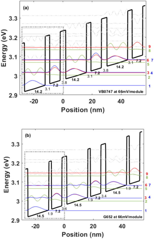
Band diagram of three sequential periods for: (a) Device VB074721 and (b) Device G65211.
Table 1.
Main nominal design parameters and devices’ data.
| Device | Layer sequence (Å)* | Al composition (%) | Doping density | E32 (meV) | E21 (meV) | Oscillator strength | Expected Tmax (K) (from NEGF calculations) | Experimental Tmax (K) |
|---|---|---|---|---|---|---|---|---|
|
VB0747 Ref.21 |
38/72/31/142 354 periods Total thickness 10 µm |
30 | Integral doping of 6.0 × 1010 cm−2 (1.26 × 1017 cm−3 in the central 48 Å in the underlined well) | 16 | 55 | 0.18 | 250 | 134 |
|
G652 Ref.11 |
34/72/19/145 371 periods Total thickness 10 µm |
30 | Integral doping of 4.5 × 1010 cm−2 (1.5 × 1017 cm−3 in the central 30 Å in the underlined well) | 16.3 | 58 | 0.29 | 250 | 250 |
*AlGaAs barriers are in bold and the GaAs wells in roman, the doped layer in the sequence is underscored.
Table 2.
Devices’ fabrication and growth parameters.
| Device | Process details | Processing laboratory | Growth laboratory |
|---|---|---|---|
|
VB0747 Ref.21 |
Metal–metal (100 Å Ta/2500 Å Au) Top contact n+ layer was removed Dry etched Mesa size 150 µm × 1.8 mm |
MIT | Sandia |
|
G652 Ref.11 |
Metal–metal (100 Å Ta/2500 Å Au) Top contact n+ layer was removed Dry etched Mesa size 150 µm × 1.23 mm |
MIT | Waterloo |
The fabrication processes for Device G652 are of excellent quality, as evidenced by the device’s ability to lase at a remarkably high temperature. Similarly, for Device VB0747, the fabrication processes are also of very high quality, validated by comparing the performance of reference designs to ensure the high quality of the processes. Additionally, Device VB0747 is the device with the lowest reported oscillator strength (~ 0.18) that was able to lase, further substantiating the overall excellent quality of the fabrication processes. This, in combination with data from other designs, led us to the conclusion that losses in all devices fabricated at MIT following this same procedure are at around 13.5 cm−1, close to the accepted values for metal–metal waveguides of ~ 15 cm−127.
We can observe in Fig. 2 a graph of the peak gain as a function of temperature for Device VB0747 (green) and Device G652 (blue). The abrupt-interface roughness height used for both calculations is 0.12 nm, a value that fits the experimental results of most clean n-level system devices. We can appreciate that the gain remains above losses for both devices up to a temperature of ~ 250 K, indicating that the slight differences in the parameters of the devices are not significant. At low temperatures, the gain is higher for Device G652, this is due to the higher oscillator strength. The relatively faster decline in the curve for Device G652 is also linked to its somewhat higher oscillator strength. The oscillator strength in Device VB0747 is slightly lower but is compensated by a higher doping density28. The different oscillator strengths can impact the lifetime of the laser levels, contributing to the observed gain differences between Device G652 and Device VB0747 at low temperatures. A higher oscillator strength reduces the lifetime of the upper laser level (ULL), whereas a reduced oscillator strength results in a longer ULL lifetime. The slower decay of the gain in Device VB0747 is in fact a result of its longer ULL lifetime. We would also like to point out that both lifetimes and oscillator strength are dependent on the bias, however we performed all our calculations at the alignment bias. The predicted Tmax is in accordance to the experimental results of Device G65211, but is far from the experimental Tmax reached by Device VB0747 (~ 134 K)21. As pointed out before, both fabrication processes are of high quality and conducted in the same laboratory following the same fabrication procedure, hence, the study identifies that the primary distinction between the two devices lies in the molecular beam epitaxy (MBE) growth.
Figure 2.
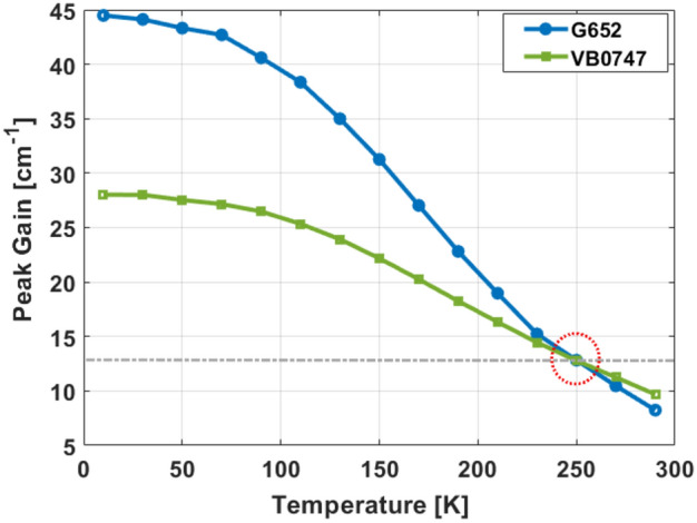
Peak gain as a function of temperature for Device VB074721 (green) and Device G65211 (blue), both with an abrupt-interface roughness height of 0.12 nm.
In accordance with this notion, all MBE-related parameters were investigated, including aluminum content, growth rate, doping density, background doping density, and abrupt-interface roughness height. By conducting a systematic study including NEGF calculations, we investigate the MBE growth related parameters, to explain the observed performance variations. Simulations based on NEGF have been instrumental in analyzing these structures29–34. NEGF is a powerful framework for predicting quantum transport in nanoscale devices, where coherent tunnelling, interference, and confinement are significant31,35. Proven effective in mid-IR QCLs36, NEGF also offers valuable insights into THz QCLs, offering detailed information on physical processes, including incoherent scattering and energy-resolved spectral functions37–40. All scattering mechanisms are considered, including electron–phonon interactions, electron–electron interactions, and interface roughness scattering. These mechanisms are all accounted for within the NEGF formalism for simulating quantum transport and optical gain in QCLs. The self-consistent updating of all scattering mechanisms during the NEGF loop enhances the precision of our simulations, contributing to the reliability and accuracy of our findings. Our studies have shown that NEGF simulations generally match experimental results when treating clean n-level systems, where electron transport is more simplified and occurs exclusively inside active states.
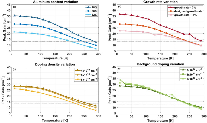
Figure 3 illustrates the temperature-dependent peak gain for Device VB0747, indicating estimated variations resulting from diverse MBE growth parameters41,42 as determined through NEGF calculations. Our calculations were done on Device VB0747 in order to understand the disparity between its experimental and calculated Tmax values. It is important to highlight that the considered error exceeded the anticipated margin to assess the worst-case scenario. The first parameter studied was the aluminum content as shown in Fig. 3a. The aluminum percentage in the barriers is calibrated based on the ratio of growth rates between gallium and aluminum. If an error in the growth rate calibration exists, it would be comparable between gallium and aluminum, and this would ensure that the ratio is still close to the desired aluminum content. The typical error margins in growth rates based on multiple calibrations is ~ 3%. For calculations purposes we considered a relatively high error of ~ 7%, this means that we considered the aluminum barrier content of Device VB0747 to be 30% ± 2%. While the expected Tmax with 30% aluminum is ~ 250 K, a lower aluminum content of 28% would mean a Tmax of ~ 280 K and increasing the content to 32% aluminum would result in a Tmax of ~ 200 K. These variations would not explain the very low Tmax of ~ 134 K observed experimentally. We believe that in this specific case, reducing the aluminum content in the barriers enhances the injection coupling, leading to better performance. Further reducing the aluminum content could not only enhance the injection coupling even more but may also reduce interface roughness (IFR) scattering. Both potential optimizations are promising areas for further research. Carrier leakage into the continuum is another factor that needs to be considered when reducing the potential barrier heights13,18–20. Understanding the complexities involved requires additional investigation to be fully comprehended.
Figure 3.
Peak gain as a function of temperature for Device VB074721 for estimated maximum variation in (a) Al content, (b) growth rate, (c) doping density, and (d) different background doping, all with an abrupt-interface roughness height of 0.12 nm.
The next variable that was studied was the total period thickness, the results are present in Fig. 3b. Correction factors for gallium and aluminum effusion sources in MBE growth are determined through reflection high-energy electron diffraction (RHEED) oscillations on a GaAs calibration wafer. Preliminary Ga(Al)As/AlGaAs superlattice structures aid in calculating these correction factors, addressing errors in growth rate calibrations. X-ray diffraction (XRD) measurements further refine the correction42. These correction factors account for errors in growth rate calibrations stemming from the physical positions of the effusion cells in the MBE reactor and are applied to rates used in QCL growth. The process includes further adjustments based on XRD period thickness, assuming any deviation is related to the total period thickness rather than composition. This two-step correction method ensures precision in achieving the desired QCL structure. Additionally, in our devices, any sample that shows an error in the structure periodicity measured by XRD of more than ± 1.5% is discarded and regrown. This relates to both Ga and Al growth rates. This minimal error in structure periodicity measured by XRD also addresses a potential deviation in the atomic fluxes through the duration of the growth. Our simulations had a growth rate error of ± 3%, which is exceptionally large given the process's precision. When considering a growth rate of 3% more than the calibrated value, the results were almost identical to the designed scheme, resulting in a Tmax of ~ 250 K. With a 3% decrease in growth rate, the Tmax reached ~ 290 K. While the temperature performance increased when the growth rate was underestimated, an overestimation of the growth rate would not explain the low experimental Tmax observed for Device VB0747.
In Fig. 3c we present the gain curves resulting from the variations in doping density, the designed doping density was of ~ 6.0 × 1010 cm−2. For calibrating the doping density, we perform a range of Hall measurements before starting a growth campaign. This involves growing multiple samples with a doped GaAs layer (different doping in each sample) followed by the execution of Hall measurements. These values are then verified before starting a QCL campaign and usual error values for doping density are ~ 15–20%. For our calculations we considered an elevated error margin of ~ 33%, which implies that we estimated the doping density of Device VB0747 to be 6.0 × 1010 cm−2 ± 2.0 × 1010 cm−2. The variations in Tmax here were even lower than when considering the aluminum content or growth rate, the Tmax for the nominal 6.0 × 1010 cm−2 doping density value was ~ 250 K while for 4.0 × 1010 cm−2 the resulting Tmax was ~ 257 K and for 8.0 × 1010 cm−2 it was ~ 215 K.
The next parameter we considered was background doping (Fig. 3d). The background doping is measured using gallium effusion cells before each campaign by growing a 19 µm-thick GaAs layer on semi-insulating GaAs substrates and performing Hall measurements. In our growths, background doping values normally range from 2.0 × 1013 cm−3 to 1.0 × 1014 cm−3, ideally the background doping would be at least an order of magnitude (if not more) below desired doping concentration in the QCL active region. However, a higher value may be expected during characterization done with dynamic SIMS (Secondary Ion Mass Spectroscopy) due to the diffusion of the dopants from higher doping areas and may not reflect the actual background doping. For our calculations, as priorly stated, we are considering the worst-case scenario, hence the values we took for the NEGF calculations were of 5 × 1014 cm−3, 5 × 1015 cm−3, and 1 × 1016 cm−3. The resulting Tmax values did not vary much yielding values in the range of ~ 240 to 250 K for all cases.
Figure 4 presents the peak gain as a function of temperature for Device VB0747. It compares the expected performance with the designed parameters (shown in green) and a worst-case scenario (in purple). In this worst-case scenario, we consider the highest errors in all MBE parameters: 32% aluminum content, a + 3% growth rate, 8.0 × 1010 cm−2 doping density, and background doping of 1 × 1016 cm−3. It is essential to highlight that these errors are intentionally set at very high levels, and the chance of all of them happening together is quite unlikely. Even under these extreme conditions, the simulation suggests a Tmax of ~ 180 K. Although this Tmax is significantly lower than the expected ~ 250 K, it still surpasses the experimental Tmax obtained for Device VB0747 (~ 134 K).
Figure 4.
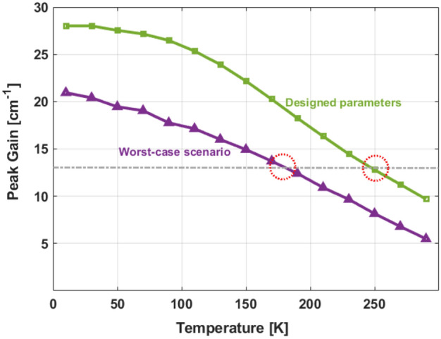
Peak Gain as a function of temperature for Device VB074721 with designed parameters (green) and worst-case scenario (purple), considering 32% Al content, + 3% growth rate, 8.0 × 1010 cm−2 doping density and background doping 1 × 1016 cm−3, both with an abrupt-interface roughness height of 0.12 nm.
From Figs. 3 and 4, it is evident that none of the investigated parameters account for the disparity between expected and experimental results for Device VB0747. Figure 5 introduces gain curves as a function of temperature, considering variations in another parameter, the abrupt-interface roughness height43–46. Without performing Atom Probe Tomography (APT)36,47,48, we cannot definitively determine whether the interfaces are graded or abrupt. However, for simplicity, we assume abrupt interfaces in our present research. For that reason, our study shows mainly trends, as there is no experimental evidence that the THz QCLs interfaces are abrupt without performing APT. In Fig. 4 we can see that while considering an abrupt-interface roughness height (∆) of ∆ = 0.12 nm results in a Tmax of ~ 250 K, an abrupt-interface roughness height of ∆ = 0.23 nm significantly reduces the Tmax value to ~ 135 K. The in-plane roughness correlation length was set as constant, and its value is Λ = 8 nm throughout all our simulations45. The Tmax values align with the experimental result obtained for Device VB0747, meaning that variations in interface roughness, even at the atomic layer level, significantly impact device performance. It is important to emphasize that interfaces with an abrupt-interface roughness height of ∆ = 0.23 nm are still considered sharp interfaces. Roughness heights around a monolayer, such as ∆ = 0.2825 nm for GaAs/AlGaAs, have been widely accepted45,49. These parameters are correct, as mentioned, when assuming abrupt interfaces. However, for graded interfaces the values may differ and two additional IFR parameters have to be considered47. For example, for mid-IR QCLs, graded interfaces have been obtained with 0.40 nm width and a roughness height of just ∆ = 0.11 nm47.
Figure 5.
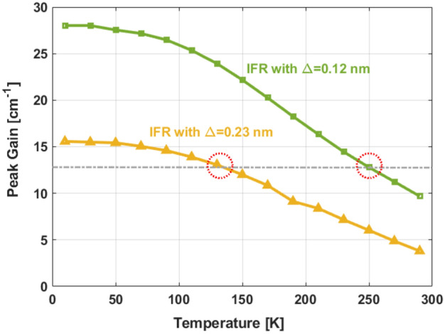
Peak gain as a function of temperature for Device VB074721 with abrupt-interface roughness height of 0.12 nm (green) and of 0.23 nm (yellow).
To further understand the implications of the variations in the IFR, in Fig. 6 we present a graph of gain as a function of photon energy at a temperature of 10 K for Device VB0747, considering abrupt-interface roughness height values of ∆ = 0.12 nm and ∆ = 0.23 nm. From the results we can see that even at low temperatures, the gain is significantly lower by a factor of almost 2 (~ 16 cm−1 as opposed to ~ 28 cm−1). Also, there is additional gain broadening. The full width at half maximum (FWHM) for the calculations corresponding to an abrupt-interface roughness height of ∆ = 0.12 nm is of ~ 8.8 meV, while for the calculations corresponding to an abrupt-interface roughness height of ∆ = 0.23 nm the FWHM is of ~ 9.3 meV, meaning that the additional gain broadening is of ~ 6%.
Figure 6.
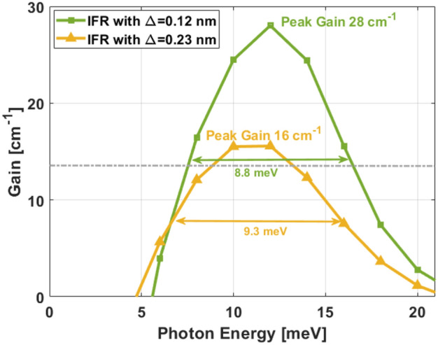
Gain as a function of photon energy for Device VB074721 at bias voltage 66 mV/module with abrupt-interface roughness height of 0.12 nm (green) and 0.23 nm (yellow).
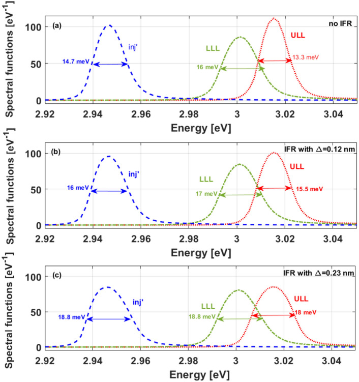
One of the factors that may affect the gain parameters is line broadening, hence, the spectral functions of the three active laser levels were analyzed. We present in Fig. 7 the spectral functions of these levels for Device VB0747, depicted in Fig. 7a without considering IFR, in Fig. 7b with an abrupt-interface roughness height of ∆ = 0.12 nm, and in Fig. 7c with an abrupt-interface roughness height of ∆ = 0.23 nm. The FWHM indicated in each figure demonstrates a slight increase in line broadening as the values of IFR rise. All levels behave similarly, so any of them can be taken as a representative level. If we take for example the upper laser level, the FWHM in Fig. 7a is ~ 13.3 meV while in Fig. 7b is ~ 15.5 meV, ~ 17% broader, and in Fig. 7c the value of the FWHM goes up to ~ 18 meV, which is 35% broader than in Fig. 7a (~ 16% broader than in Fig. 7b). From these results we conclude that the light changes in the abrupt-interface roughness height cause an increased line broadening, which may partially explain the gain decrease and consequently poor temperature performance. Previous studies20,45,49 support our findings, showing the significant influence of IFR scattering on GaAs/AlxGa1−xAs THz QCLs. Reference45 emphasizes that narrower wells cause greater linewidth and gain broadening. Despite this, the importance of quantum wells thinner than 35 monolayers in reducing thermally activated leakage into excited states is highlighted. Therefore, given our adoption of narrow wells to achieve a clean 3-level system, these conclusions directly apply to our devices. A more significant factor than line broadening affecting the gain and maximum QCL operating temperature is likely intense IFR-triggered non-radiative leakage. The IFR scattering rate is a strong function of ∆ and is proportional to the square of the conduction-band offset, which is significant for state-of-the-art THz QCLs. One possibility is IFR-triggered non-radiative leakage from the upper laser level to the lower laser level, which could explain the inferior performance. However, there is currently insufficient experimental or theoretical evidence in the literature to support such a mechanism. Alternatively, carrier leakage triggered by intense IFR scattering rate has been observed in mid-IR QCLs46,47, with the leakage being a shunt-type current through at least one excited state. Then, assuming for simplicity one high-energy state, a clean 4-level system will need to be used for device analysis; that is, include one high-energy excited state through which shunt-type current occurs, similar to what was recently done for the multi-band NEGF model employed for mid-infrared QCLs47.
Figure 7.
Spectral functions of the ground levels for Device VB074721 (a) without IFR, (b) with abrupt-interface roughness height of 0.12 nm, and (c) with abrupt-interface roughness height of 0.23 nm. FWHH included in each figure.
Based on the obtained results, it can be concluded that subtle variations in the abrupt-interface roughness height lead to substantial effects on the performance of THz QCLs. The Tmax values turned out to be particularly sensitive to the changes in IFR, as opposed to the variations in other parameters that did not lead to a substantial impact on Tmax. Minor changes in abrupt-interface roughness height contribute to an increased line broadening and a decreased gain, ultimately resulting in diminished temperature performance and indicating that even marginal deviations at the atomic layer level can significantly affect the laser levels characteristics. The observed sensitivity of the THz QCLs to such slight modifications underscores the critical role played by IFR in determining temperature performance. The systematic comparison between two devices with nearly identical parameters but grown at different MBE laboratories provides valuable insights into the sensitivity of these structures to IFR. The NEGF calculations proved instrumental in understanding the impact of various MBE-related parameters.
Additionally, the observed disparity in Tmax between the two devices, despite high-quality fabrication processes, points to the need for a deeper comprehension of MBE crystal growth conditions. Achieving reproducible and high-performance THz QCLs necessitates careful optimization of MBE growth, with particular attention to maintaining high interface sharpness. Achieving interfaces sharper than those described may pose a significant challenge, however, if accomplished, it holds the potential to surpass previous records in THz QCL temperature performance. Interface engineering, for example, by using graded interface modelling, as has been done effectively for mid-IR QCLs36,47, is another suggested option for interface optimization. Although the use of graded interfaces proved to be beneficial for mid-IR QCLs, it is crucial to acknowledge the need for specific investigations tailored to THz QCLs. We suggest APT48 as a path to analyze and extract the IFR parameters, in order to reduce IFR scattering and substantially improve the performance of THz QCLs, as done for mid-IR QCLs47. Additionally, once optimized interfaces are indeed achieved, engineering of the doping density, its spatial location and its profile may lead to even higher temperatures50. This study contributes not only to the fundamental understanding of THz QCLs but also provides practical guidance for researchers aiming to further enhance the temperature performance of these devices.
Another path for future improvements is reducing the layers’ thicknesses, enhancing this way the injection coupling. As demonstrated in our results with a 3% decrease in growth rate, the Tmax reached approximately 290 K, indicating the potential for achieving room temperature performance.
In conclusion, our study highlights a significant performance gap between two TW THz QCLs supporting clean 3-level systems with nearly identical parameters. Despite NEGF calculations predicting a Tmax of ~ 250 K for both devices, experimental results show one device reaching this Tmax while the other peaks at only ~ 134 K. The very similar design parameters and high-quality fabrication processes, as confirmed by reference devices, point to MBE growth as the distinguishing factor. Our detailed NEGF-based analysis scrutinized various MBE-related parameters, revealing that minor differences in interface roughness significantly impact device performance. This study identifies the critical parameter still limiting the temperature performance of THz QCLs, overcoming this limitation would require extremely precise MBE crystal growth conditions. Experimental work, using techniques like APT, is needed to better understand interface structure and optimize interfaces. In addition, doping engineering could potentially enhance the temperature performance of THz QCLs but only after optimized interfaces are achieved50. Our study not only addresses challenges faced by other groups in reproducing the Tmax of ~ 250 K and ~ 261 K but also proposes a systematic pathway for further improving the temperature performance of THz QCLs beyond the state-of-the-art.
Acknowledgements
The authors would like to acknowledge the Israel Science Foundation (ISF 1755/23) for its grant. This work was performed, in part, at the Center for Integrated Nanotechnologies, an Office of Science User Facility operated for the U.S. Department of Energy (DOE) Office of Science. Sandia National Laboratories is a multi-mission laboratory managed and operated by National Technology & Engineering Solutions of Sandia, LLC, a wholly owned subsidiary of Honeywell International, Inc., for the U.S. DOE’s National Nuclear Security Administration under contract DE-NA-0003525. The views expressed in the article do not necessarily represent the views of the U.S. DOE or the United States Government.
Author contributions
N.L.G. did the formal analysis and wrote and edited the original draft, S.L. and S.P. conducted part of the investigation, S.J.A. gave insights on the methodology and resources for the investigation, A.A. lead the investigation including the writing, project administration, funding acquisition and supervision. All authors reviewed the manuscript.
Data availability
The datasets generated and/or analysed during the current study are available from the corresponding author upon reasonable request.
Competing interests
The authors declare no competing interests.
Footnotes
Publisher's note
Springer Nature remains neutral with regard to jurisdictional claims in published maps and institutional affiliations.
References
- 1.Köhler, R. et al. Terahertz semiconductor-heterostructure laser. Nature417(6885), 156–159 (2002). 10.1038/417156a [DOI] [PubMed] [Google Scholar]
- 2.Faist, J. et al. Quantum cascade laser. Science264(5158), 553–556 (1994). 10.1126/science.264.5158.553 [DOI] [PubMed] [Google Scholar]
- 3.Williams, B. S. Terahertz quantum-cascade lasers. Nat. Photon.1(9), 517–525 (2007). 10.1038/nphoton.2007.166 [DOI] [Google Scholar]
- 4.Woolard, D. L., Brown, R., Pepper, M. & Kemp, M. Terahertz frequency sensing and imaging: A time of reckoning future applications?. Proc. IEEE93(10), 1722–1743 (2005). 10.1109/JPROC.2005.853539 [DOI] [Google Scholar]
- 5.Vitiello, M. S. & Tredicucci, A. Physics and technology of Terahertz quantum cascade lasers. Adv. Phys. X6(1), 1893809 (2021). [Google Scholar]
- 6.Lin, T.-T., Wang, L., Wang, K., Grange, T., Birner, S. & Hirayama, H. Over 1 watt THz QCLs with high doping concentration and variable Al composition in active structure. In Conference on Lasers and Electro-Optics SS2D.6 (Optica Publishing Group, 2022).
- 7.Li, L. H. et al. Multi-watt high-power THz frequency quantum cascade lasers. Electron. Lett.53(12), 799–800 (2017). 10.1049/el.2017.0662 [DOI] [Google Scholar]
- 8.Khalatpour, A. et al. Enhanced operating temperature in terahertz quantum cascade lasers based on direct phonon depopulation. Appl. Phys. Lett.122(16), 161101 (2023). 10.1063/5.0144705 [DOI] [Google Scholar]
- 9.Wen, B. & Ban, D. High-temperature terahertz quantum cascade lasers. Prog. Quantum Electron.80, 100363 (2021). 10.1016/j.pquantelec.2021.100363 [DOI] [Google Scholar]
- 10.Rindert, V., Önder, E. & Wacker, A. Analysis of high performing terahertz quantum cascade lasers. Phys. Rev. Appl.18, L041001 (2022). 10.1103/PhysRevApplied.18.L041001 [DOI] [Google Scholar]
- 11.Khalatpour, A., Paulsen, A. K., Deimert, C., Wasilewski, Z. R. & Hu, Q. High-power portable terahertz laser systems. Nat. Photon.15(1), 16–20 (2021). 10.1038/s41566-020-00707-5 [DOI] [Google Scholar]
- 12.Gower, N. L. et al. Extraction of the electron excess temperature in terahertz quantum cascade lasers from laser characteristics. Nanophotonics13(10), 1725–1733 (2024). 10.1515/nanoph-2023-0617 [DOI] [Google Scholar]
- 13.Albo, A. & Flores, Y. V. Temperature-driven enhancement of the stimulated emission rate in terahertz quantum cascade lasers. IEEE J. Quantum Electron.53(1), 1–5 (2017). 10.1109/JQE.2016.2631899 [DOI] [Google Scholar]
- 14.Albo, A. & Hu, Q. Investigating temperature degradation in THz quantum cascade lasers by examination of temperature dependence of output power. Appl. Phys. Lett.106(13), 131108 (2015). 10.1063/1.4916961 [DOI] [Google Scholar]
- 15.Burghoff, D. Beyond pulses: Frequency combs in active cavities. In 2022 IEEE Photonics Society Summer Topicals Meeting Series (SUM) 1–2 (2022).
- 16.Curwen, C. A., Kawamura, J. H., Hayton, D. J., Wu, Y., Addamane, S. J., Reno, J. L., Williams, B. S. & Karasik, B. S. Terahertz quantum-cascade VECSELs local oscillators for heterodyne receivers. In Millimeter, Submillimeter, and Far-Infrared Detectors and Instrumentation for Astronomy XI Vol. PC12190 (eds Zmuidzinas, J. & Gao J.-R.) PC121900A (SPIE, 2022).
- 17.Kao, T.-Y., Reno, J. L. & Hu, Q. Amplifiers of free-space terahertz radiation. Optica4(7), 713–716 (2017). 10.1364/OPTICA.4.000713 [DOI] [Google Scholar]
- 18.Albo, A. & Flores, Y. V. Carrier leakage dynamics in terahertz quantum cascade lasers. IEEE J. Quantum Electron.53(5), 1–8 (2017). 10.1109/JQE.2017.2740261 [DOI] [Google Scholar]
- 19.Albo, A. & Hu, Q. Carrier leakage into the continuum in diagonal GaAs/Al0.15GaAs terahertz quantum cascade lasers. Appl. Phys. Lett.107(24), 241101 (2015). 10.1063/1.4937455 [DOI] [Google Scholar]
- 20.Albo, A., Hu, Q. & Reno, J. L. Room temperature negative differential resistance in terahertz quantum cascade laser structures. Appl. Phys. Lett.109(8), 081102 (2016). 10.1063/1.4961617 [DOI] [Google Scholar]
- 21.Albo, A., Flores, Y. V., Hu, Q. & Reno, J. L. Two-well terahertz quantum cascade lasers with suppressed carrier leakage. Appl. Phys. Lett.111(11), 111107 (2017). 10.1063/1.4996567 [DOI] [Google Scholar]
- 22.Albo, A., Flores, Y. V., Hu, Q. & Reno, J. L. Split-well direct-phonon terahertz quantum cascade lasers. Appl. Phys. Lett.114(19), 191102 (2019). 10.1063/1.5089854 [DOI] [Google Scholar]
- 23.Lander Gower, N., Piperno, S. & Albo, A. The significance of carrier leakage for stable lasing in split-well direct phonon terahertz quantum cascade lasers. Photonics7(3), 59 (2020). 10.3390/photonics7030059 [DOI] [Google Scholar]
- 24.Levy, S., Gower, N. L., Piperno, S., Addamane, S. J., Reno, J. L. & Albo, A. (2023) Novel split-well resonant-phonon terahertz quantum cascade laser supporting clean four-level system. In 2023 48th International Conference on Infrared, Millimeter, and Terahertz Waves (IRMMW-THz) 1–2 (2023).
- 25.Levy, S. et al. Split-well resonant-phonon terahertz quantum cascade laser. Opt. Express31(14), 22274–22283 (2023). 10.1364/OE.486446 [DOI] [PubMed] [Google Scholar]
- 26.Lander Gower, N. et al. Two-well injector direct-phonon terahertz quantum cascade lasers. Appl. Phys. Lett.123(6), 061109 (2023). 10.1063/5.0155250 [DOI] [Google Scholar]
- 27.Wienold, M. et al. High-temperature, continuous-wave operation of terahertz quantum-cascade lasers with metal-metal waveguides and third-order distributed feedback. Opt. Express22(3), 3334–3348 (2014). 10.1364/OE.22.003334 [DOI] [PubMed] [Google Scholar]
- 28.Chan, C. W. I., Albo, A., Hu, Q. & Reno, J. L. Tradeoffs between oscillator strength and lifetime in terahertz quantum cascade lasers. Appl. Phys. Lett.109, 201104 10.1063/1.4967244 (2016). 10.1063/1.4967244 [DOI] [Google Scholar]
- 29.Grange, T. et al. Room temperature operation of n-type Ge/SiGe terahertz quantum cascade lasers predicted by non-equilibrium Green’s functions. Appl. Phys. Lett.114(11), 111102 (2019). 10.1063/1.5082172 [DOI] [Google Scholar]
- 30.Lander Gower, N., Piperno, S. & Albo, A. Self-consistent gain calculations and carrier transport analysis for split-well direct-phonon terahertz quantum cascade lasers. AIP Adv.10(11), 115319 (2020). 10.1063/5.0015952 [DOI] [Google Scholar]
- 31.Lee, S.-C. & Wacker, A. Nonequilibrium Green’s function theory for transport and gain properties of quantum cascade structures. Phys. Rev. B66(24), 245314 (2002). 10.1103/PhysRevB.66.245314 [DOI] [Google Scholar]
- 32.Gower, N. L., Piperno, S. & Albo, A. The response of split-well direct-phonon THz quantum-cascade laser structures to changes in doping. In 2022 47th International Conference on Infrared, Millimeter and Terahertz Waves (IRMMW-THz) 1–2 (2022).
- 33.Lander Gower, N., Piperno, S. & Albo, A. Comparison of THz-QCL designs supporting clean N-level systems. Photonics8(7), 248 (2021). 10.3390/photonics8070248 [DOI] [Google Scholar]
- 34.Lander-Gower, N., Piperno, S. & Albo, A. The effect of doping in split-well direct-phonon THz quantum-cascade laser structures. Photonics8(6), 195 (2021). 10.3390/photonics8060195 [DOI] [Google Scholar]
- 35.Kubis, T. et al. Theory of nonequilibrium quantum transport and energy dissipation in terahertz quantum cascade lasers. Phys. Rev. B79(19), 195323 (2009). 10.1103/PhysRevB.79.195323 [DOI] [Google Scholar]
- 36.Suri, S., Knipfer, B., Grange, T., Guo, H., Kirch, J. D., Mawst, L. J., Marsland, R. A. & Botez, D. Graded-interfaces modeling of record-performance mid and long-wave infrared quantum cascade lasers. In Novel In-Plane Semiconductor Lasers XXII PC12440 (eds Belyanin, A. A. & Smowton, P. M.) PC124400U (SPIE, 2023).
- 37.Grange, T. Electron transport in quantum wire superlattices. Phys. Rev. B89(16), 165310 (2014). 10.1103/PhysRevB.89.165310 [DOI] [Google Scholar]
- 38.Grange, T. Nanowire terahertz quantum cascade lasers. Appl. Phys. Lett.105(14), 141105 (2014). 10.1063/1.4897543 [DOI] [Google Scholar]
- 39.Grange, T. Contrasting influence of charged impurities on transport and gain in terahertz quantum cascade lasers. Phys. Rev. B92, 241306 (2015). 10.1103/PhysRevB.92.241306 [DOI] [Google Scholar]
- 40.Jirauschek, C. & Kubis, T. Modeling techniques for quantum cascade lasers. Appl. Phys. Rev.1(1), 011307 (2014). 10.1063/1.4863665 [DOI] [Google Scholar]
- 41.Li, L. H., Zhu, J. X., Chen, L., Davies, A. G. & Linfield, E. H. The MBE growth and optimization of high performance terahertz frequency quantum cascade lasers. Opt. Express23(3), 2720–2729 (2015). 10.1364/OE.23.002720 [DOI] [PubMed] [Google Scholar]
- 42.Beere, H. E. et al. MBE growth of terahertz quantum cascade lasers. J. Cryst. Growth278(1), 756–764 (2005). 10.1016/j.jcrysgro.2004.12.172 [DOI] [Google Scholar]
- 43.Flores, Y. V., Kurlov, S. S., Elagin, M., Semtsiv, M. P. & Masselink, W. T. Leakage current in quantum-cascade lasers through interface roughness scattering. Appl. Phys. Lett.103(16), 161102 (2013). 10.1063/1.4825229 [DOI] [Google Scholar]
- 44.Botez, D., Chang, C.-C. & Mawst, L. J. Temperature sensitivity of the electro-optical characteristics for mid-infrared (λ = 3–16 µm)-emitting quantum cascade lasers. J. Phys. Appl. Phys.49(4), 043001 (2015). 10.1088/0022-3727/49/4/043001 [DOI] [Google Scholar]
- 45.Flores, Y. V. & Albo, A. Impact of interface roughness scattering on the performance of GaAs/AlxGa1–xAs terahertz quantum cascade lasers. IEEE J. Quantum Electron.53(3), 1–8 (2017). 10.1109/JQE.2017.2689743 [DOI] [Google Scholar]
- 46.Boyle, C. et al. Carrier leakage via interface-roughness scattering bridges gap between theoretical and experimental internal efficiencies of quantum cascade lasers. Appl. Phys. Lett.117(5), 051101 (2020). 10.1063/5.0007812 [DOI] [Google Scholar]
- 47.Suri, S. et al. Modeling with graded interfaces: Tool for understanding and designing record-high power and efficiency mid-infrared quantum cascade lasers. Nanophotonics13(10), 1745–1757 (2024). 10.1515/nanoph-2023-0687 [DOI] [Google Scholar]
- 48.Knipfer, B., Xu, S., Kirch, J. D., Botez, D. & Mawst, L. J. Analysis of interface roughness in strained InGaAs/AlInAs quantum cascade laser structures (λ ∼ 4.6 µm) by atom probe tomography. J. Cryst. Growth583, 126531 (2022). 10.1016/j.jcrysgro.2022.126531 [DOI] [Google Scholar]
- 49.Chan, C. W. I., Hu, Q. & Reno, J. L. Tall-barrier terahertz quantum cascade lasers. Appl. Phys. Lett.103(15), 151117 (2013). 10.1063/1.4824878 [DOI] [Google Scholar]
- 50.Lander Gower, N. et al. Doping engineering: Next step toward room temperature performance of terahertz quantum cascade lasers. J. Vac. Sci. Technol. B42(1), 010801 (2024). 10.1116/6.0003160 [DOI] [Google Scholar]
Associated Data
This section collects any data citations, data availability statements, or supplementary materials included in this article.
Data Availability Statement
The datasets generated and/or analysed during the current study are available from the corresponding author upon reasonable request.


