

ABSTRACT
The number and stacking order of layers are two important degrees of freedom that can modulate the properties of 2D van der Waals (vdW) materials. However, the layers’ structures are essentially limited to the known layered 3D vdW materials. Recently, a new 2D vdW material, MoSi2N4, without known 3D counterparts, was synthesized by passivating the surface dangling bonds of non-layered 2D molybdenum nitride with elemental silicon, whose monolayer can be viewed as a monolayer MoN (-N-Mo-N-) sandwiched between two Si-N layers. This unique sandwich structure endows the MoSi2N4 monolayer with many fascinating properties and intriguing applications, and the surface-passivating growth method creates the possibility of tuning the layer's structure of 2D vdW materials. Here we synthesized a series of MoSi2N4(MoN)4n structures confined in the matrix of multilayer MoSi2N4. These super-thick monolayers are the homologous compounds of MoSi2N4, which can be viewed as multilayer MoN (Mo4n+1N4n+2) sandwiched between two Si-N layers. First-principles calculations show that MoSi2N4(MoN)4 monolayers have much higher Young's modulus than MoN, which is attributed to the strong Si-N bonds on the surface. Importantly, different from the semiconducting nature of the MoSi2N4 monolayer, the MoSi2N4(MoN)4 monolayer is identified as a superconductor with a transition temperature of 9.02 K. The discovery of MoSi2N4(MoN)4n structures not only expands the family of 2D materials but also brings a new degree of freedom to tailor the structure of 2D vdW materials, which may lead to unexpected novel properties and applications.
Keywords: MoSi2N4, 2D layered materials, homologous compounds, iDPC-STEM, superconductivity
We discovered superconducting homologous compounds of 2D MoSi2N4, MoSi2N4(MoN)4n, which provides a new strategy to tailor the structure and properties of 2D materials by phase homology.
INTRODUCTION
Van der Waals (vdW) layered materials have strong in-plane chemical bonds but weak interaction between adjacent layers, and therefore readily approach two-dimensional (2D) limits by diverse methods. This leads to many layer-dependent novel phenomena and unique properties that are absent in their three-dimensional (3D) bulk counterparts [1–14]. For example, monolayer graphene is a gapless semimetal, while bilayer graphene shows a gate-tunable bandgap or superconducting properties depending on the stacking order [1,6,15,16]; monolayer MoS2 is a direct bandgap semiconductor, whereas multilayer MoS2 is an indirect bandgap semiconductor [8]; monolayer CrI3 is an Ising ferromagnet, while bilayer CrI3 displays suppressed magnetization with a metamagnetic effect [17]. Therefore, the number and stacking of layers are two important degrees of freedom that can modulate the properties of vdW layered 2D materials. However, the layers’ structures are essentially limited to the known 3D layered vdW materials. Making a multiple-atomic-layer unit using vdW heterostructures of different 2D crystals creates a new possibility of tuning the layer properties of 2D materials. For example, MnBi2Te4/Bi2Te3 superlattices exhibit many exotic physical phenomena such as an intrinsic ferromagnetic topological state [18], large magnetic gap [19], quantum anomalous Hall regime [20] and controllable magnetic properties [21]. However, the unit in such a material as MnBi2Te4/Bi2Te3 is integrated by vdW interaction rather than the chemical bonding that is present in the layer of vdW materials.
Recently, we synthesized a new septuple-atomic-layer 2D vdW material without known 3D counterpart, MoSi2N4, by passivating the surface dangling bonds of non-layered 2D molybdenum nitride with elemental silicon in a chemical vapor deposition (CVD) process [22]. The MoSi2N4 monolayer can be viewed as a MoN2 layer sandwiched between two Si-N layers via chemical bonds, in which the MoN2 layer is a unit-cell-thick MoN slice (-N-Mo-N-) with N-terminating atomic layers on both sides, i.e. monolayer MoN. The structure of such a unique sandwiched layer means that monolayer MoSi2N4 is a very stable 2D semiconductor with potentially higher carrier mobility and better mechanical strength than monolayer MoS2. Furthermore, it is expected to have valley-contrasting properties, anomalous high thermal conductivity, outstanding optical properties, piezoelectricity, ferroelectricity, magnetic properties, efficient Ohmic contacts and photocatalytic and electrocatalytic activities with potential applications in valleytronics, nanoelectronics, optoelectronics and energy conversion [23–39]. Importantly, many such sandwich-structured 2D vdW materials with a general formula of MA2Z4 have been predicted [22,40,41], which will further expand the properties of 2D materials, and the surface-passivating CVD growth method creates the possibility of tailoring the layer structures of such 2D vdW materials.
Here, we synthesized a series of super-thick sandwich-structured vdW monolayers with a formula of MoSi2N4(MoN)4n confined in the matrix of MoSi2N4 multilayer crystals by surface-passivating CVD. These super-thick monolayers are the homologous compounds of MoSi2N4, which can be viewed as multilayer MoN (Mo4n+1N4n+2) sandwiched between two Si-N layers. Among them, MoSi2N4(MoN)4 is predicted to be a phonon-mediated superconductor with a transition temperature of 9.02 K, and to have a higher Young's modulus than MoN. The discovery of MoSi2N4(MoN)4n structures not only expands the family of 2D materials but also brings a new degree of freedom with which to tailor the structure of 2D vdW materials.
RESULTS
MoSi2N4(MoN)4n homogenous compounds were synthesized by the surface-passivating CVD, similar to the growth of MoSi2N4 [22]. A Cu/Mo bilayer was used as the substrate with the underlying Mo foil as Mo source, NH3 gas as the nitrogen source and a quartz plate as silicon source. The feeding rate of NH3 gas plays a key role in the structure of the products. At a low feeding rate of NH3 (3 sccm), strict monolayer MoSi2N4 film was obtained, whereas multilayer MoSi2N4 flakes were synthesized with increasing the flow rate of NH3. All the structures were characterized by recently developed integrated and differentiated differential phase contrast (iDPC and dDPC) scanning transmission electron microscopy (STEM) techniques [42–44]. The iDPC- and dDPC-STEM linearly correspond to the electrostatic potential field and charge density distribution field of a thin sample, respectively [42]. For high-angle annular dark-field (HAADF) STEM, it is challenging to image the light elements such as H, C, N, O in crystalline materials, especially for those containing heavy elements, since HAADF intensity is roughly proportional to Z2 (Z, atomic number) [45]. However, the iDPC intensity is roughly proportional to Z, thus giving rise to much stronger contrast enhancement of light elements among heavy elements [46].
We first characterized the crystalline structure of MoSi2N4; the N atomic occupation and layer stacking sequences had not been experimentally confirmed in our previous work [22]. Different from HAADF-STEM images, the cross-sectional iDPC- and dDPC-STEM images clearly show the exact sites of all the N atoms in MoSi2N4 besides Mo and Si, which form a coupling configuration of tetrahedra and triangular prisms around Si and Mo, respectively (Fig. 1a and b). This structure is completely consistent with our reported MoSi2N4 structure in which the N atomic occupation was finally confirmed by density functional theory (DFT) calculations [22].
Figure 1.
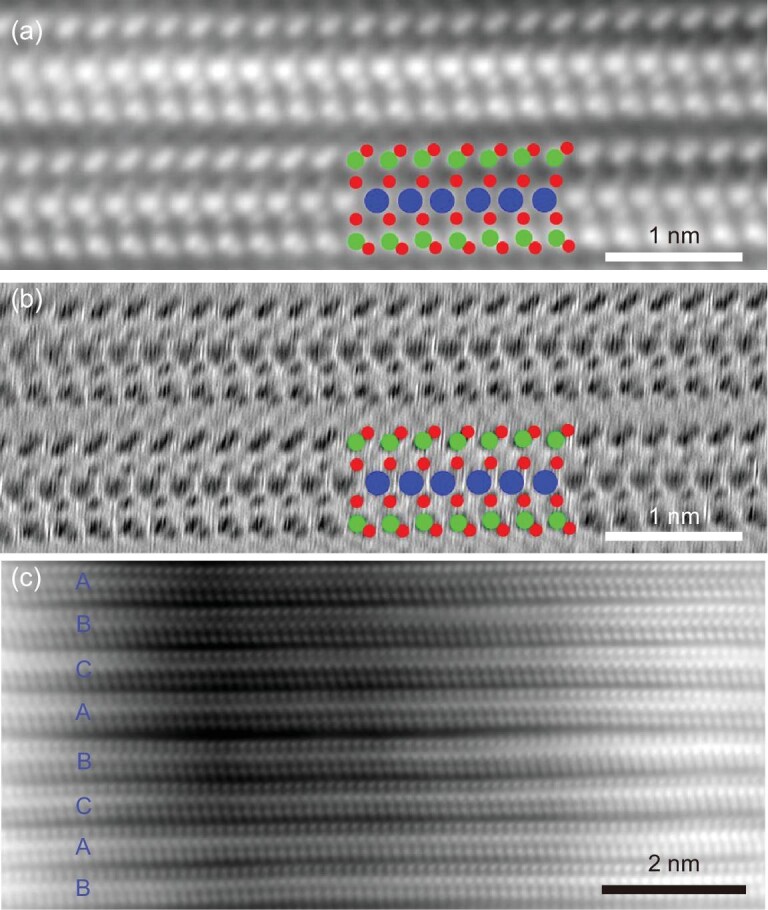
The atomic structure of multilayer MoSi2N4. (a and b) iDPC (a) and the corresponding dDPC (b) images of bilayer MoSi2N4, clearly showing the atomic sites of Mo (blue balls), Si (green balls) and N (red balls). (c) iDPC image of a rhombohedral-structured multilayer MoSi2N4 with ABC-typed stacking order.
The stacking order of MoSi2N4 layers determines the 3D
crystallographic structure of MoSi2N4 bulk phase. From a geometric
point of view, there are multiple stacking orders for MoSi2N4 layers
including AA, AB, A , A
, A ,
A
,
A and ABC. The symbols of
 ,
,  ,
,
 represent 180° rotation
against A, B, C, respectively. Supplementary Table S1 shows the formation energies of different stacking orders
(corresponding atomic models shown in Supplementary Fig. S1), in which the ABC-stacked MoSi2N4
phase is more energy-preferable. By checking dozens of samples, we found that ABC stacking
shows the preference of long-range order compared with AA and AB stacking (Fig. 1c and Supplementary Fig. S2), while A
represent 180° rotation
against A, B, C, respectively. Supplementary Table S1 shows the formation energies of different stacking orders
(corresponding atomic models shown in Supplementary Fig. S1), in which the ABC-stacked MoSi2N4
phase is more energy-preferable. By checking dozens of samples, we found that ABC stacking
shows the preference of long-range order compared with AA and AB stacking (Fig. 1c and Supplementary Fig. S2), while A ,
A
,
A , A
, A stacking orders were not observed. Therefore, the CVD-grown multilayer
MoSi2N4 materials are predominantly rhombohedral-structured crystals
with ABC stacking, whose crystallographic information is displayed in Supplementary Table S2.
stacking orders were not observed. Therefore, the CVD-grown multilayer
MoSi2N4 materials are predominantly rhombohedral-structured crystals
with ABC stacking, whose crystallographic information is displayed in Supplementary Table S2.
Importantly, a thicker MoSi2N4(MoN)4 monolayer structure was formed in the matrix of multilayer MoSi2N4 by introducing more NH3. Large-field STEM images show that this structure looks like a MoSi2N4 intercalation compound (Supplementary Fig. S3), in which the intercalant contains Mo and N, confirmed by electron energy loss spectroscopy (EELS) (Supplementary Fig. S4). HAADF-STEM images show that it is composed of five Mo atomic layers sandwiched by two Si atomic layers (Fig. 2a and b). Further iDPC- and dDPC-STEM characterizations reveal eight N atomic layers interdigitating with Mo and Si layers, in which four internal N layers occupy the interstitial sites of triangular prisms and a peculiar layer of octahedra of Mo frame to form a MoN configuration, while the four external N layers form Si-N tetrahedra with the two Si atomic layers on two sides (Fig. 2c and d). These results suggest that the MoSi2N4(MoN)4 layer is built up by 15 atomic layers and can be viewed as a five-layer MoN (Mo5N6) sandwiched between two Si-N layers. In this structure, the two outer Mo atomic layers align with the multilayer MoSi2N4 matrix. The spatial confinement effect of the MoSi2N4 matrix results in the formation of a Mo octahedron stacking fault layer (Fig. 2b), which reduces the volume expansion of MoSi2N4(MoN)4 in the MoSi2N4 matrix (Supplementary Fig. S5).
Figure 2.
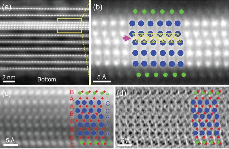
The atomic structure of MoSi2N4(MoN)4. (a and b) HAADF-STEM image of MoSi2N4(MoN)4 confined in multilayer MoSi2N4 (a) and the zoomed-in view of the MoSi2N4(MoN)4 (b). (c and d) iDPC (c) and dDPC (d) images of MoSi2N4(MoN)4. The blue, green and red balls represent the Mo, Si and N atoms, respectively.
Phase homology refers to a series of compounds built on the same structural principle with certain modules expanding in various dimensions by regular increments [47,48]. Thus, MoSi2N4(MoN)4 is a homologous compound of MoSi2N4 based on the structural expansion of internal MoN configuration. Notably, MoSi2N4(MoN)4 is different from the intercalated compounds, in which guest species such as atoms, ions and molecules occupy the interlayer space of vdW layered crystals without changing the layers’ structures [49–52]. It is also different from the recently reported covalently bonded 2D layered materials engineered by self-intercalation, where the intercalated atomic layers covalently bond to pristine 2D materials [49].
Interestingly, much thicker homologous MoSi2N4(MoN)4n monolayers with n = 2, 3, 4, 5, 6, 7, 8, 9, 10 can also be synthesized (Fig. 3 and Supplementary Fig. S6). Figure 3a and b show the HAADF and iDPC images of MoSi2N4(MoN)8, respectively. Note that the Mo atomic layers aligned with the MoSi2N4 matrix maintain stable ABC stacking, the same as the pure MoSi2N4 multilayers, suggesting that they inherited the structure of the matrix. Like MoSi2N4(MoN)4, the two outermost Si-N layers of MoSi2N4(MoN)8 are preserved, while the others are replaced with Mo-N layers. The MoSi2N4(MoN)8 layer is built up by 23 atomic layers and can be viewed as a nine-layer MoN (Mo9N10) sandwiched between two Si-N layers (Fig. 3b). Figure 3c exhibits the HAADF image of a super-thick MoSi2N4(MoN)40 containing 87 atomic layers, which is the thickest vdW monolayer structure reported so far. As shown in the iDPC image (Fig. 3d), all the MoN configurations are similar in between the Mo atomic layers aligned with the MoSi2N4 matrix, forming a consecutive MoN phase (Supplementary Fig. S7). However, we have also observed MoSi2N4(MoN)4n isomers with different N arrangements on the surface and/or mirror-symmetric Mo-N inner layers (Supplementary Fig. S8). In principle, the thickness of the homologous compound MoSi2N4(MoN)4n monolayer can be further increased.
Figure 3.

The atomic structure of super-thick MoSi2N4(MoN)4n. (a and b) HAADF-STEM image of MoSi2N4(MoN)8 confined in multilayer MoSi2N4 (a) and iDPC image of MoSi2N4(MoN)8 (b). The A, B and C lines indicate the Mo atomic layers aligned with the MoSi2N4 matrix. (c and d) HAADF-STEM image of one end of the MoSi2N4(MoN)4n confined in 11-layer MoSi2N4 (c) and iDPC image of MoSi2N4(MoN)28 (d). The blue, green and red balls represent the Mo, Si and N atoms, respectively.
The formation of MoSi2N4(MoN)4n in the matrix of MoSi2N4 shows the potential for tailoring the layer structures of 2D vdW materials by changing the number of sandwiched MoN layers. It is reasonable to expect that isolated MoSi2N4(MoN)n could be synthesized by precisely designing the growth process and parameters. We used first-principles DFT calculations to evaluate the structure and properties of the MoSi2N4(MoN)n with n = 1−4. By changing the positions of Mo and N atoms based on the symmetry analyses and structural screening, energetically favorable atomic structures were obtained for each MoSi2N4(MoN)n, as shown in Supplementary Fig. S9; these are dynamically stable without any imaginary frequencies found in the phonon dispersions (Supplementary Fig. S10). The calculated energetically favorable structure of isolated MoSi2N4(MoN)4 screened from 512 candidates contains only MoN triangular prisms (Fig. 4a and b), which are slightly different from the experimentally observed ones confined in bilayer MoSi2N4 (Fig. 2c and d). The energy of the calculated MoSi2N4(MoN)4 structure is 0.108 eV/atom lower than that of the experimental structure. The presence of the stacking fault layer leads to a small difference in the electronic band structures, but both show metallic characteristics (Fig. 4c). To identify the uniqueness of these homologous compounds, we studied the energetically favorable isolated MoSi2N4(MoN)n via a comparison with the corresponding sandwiched Mon+1Nn+2 (Supplementary Fig. S11).
Figure 4.

Calculated structures and properties of MoSi2N4(MoN)n. (a) Diagram illustrating the process of structure screening of MoSi2N4(MoN)4. (b and c) The atomic models (b) and electronic band structures (c) of the energetically favorable structure and experimental structure of MoSi2N4(MoN)4. (d) Young's modulus of MoSi2N4(MoN)n and Mon+1Nn+2 for n = 0−4. The Young's modulus of Mo2N3 was not given due to its mechanical instability. (e and f) Phonon dispersions, vibrational PHDOS, Eliashberg function and accumulated EPC constants of MoSi2N4(MoN)4 (e) and Mo5N6 (f), where the circles in phonon dispersion plots represent the phonon linewidth γqν, related to the contribution to α2F(ω) at each q and each mode ν.
Figure 4d and Supplementary Table S3 show that MoSi2N4(MoN)n (n = 0−4) has much higher Young's modulus than the sandwiched Mon+1Nn+2. The Young's modulus of Mon+1Nn+2 strongly depends on the number of MoN layers, which approaches that of bulk MoN crystals (431.32 GPa) at four layers. In contrast, the Young's modulus of MoSi2N4(MoN)n only shows slight changes with the number of MoN layers. These results suggest the significant contribution of the outmost Si-N layers to the excellent mechanical properties of MoSi2N4(MoN)n. To understand the physical origin, we analyzed the bonding characteristics of MoSi2N4(MoN)n and Mon+1Nn+2 compounds by deriving the electron localization function (ELF). ELF = 1 and ELF = 0 mean perfect electron localization and delocalization, respectively, while ELF = 0.5 corresponds to the electron-gas-like pair probability [53]. As shown in Supplementary Fig. S12, the electrons are largely localized around N atoms, which indicates the ionic bond characteristics of Mo-N bonds and Si-N bonds in the MoSi2N4(MoN)n and Mon+1Nn+2 (n = 0−4). Compared to Mo atoms, the almost-zero ELF value around Si atoms suggests no valence electrons around Si atoms, indicating that Si-N bonds are much stronger than Mo-N bonds. Therefore, the surface Si-N layers are responsible for the superior Young's modulus of MoSi2N4(MoN)n.
More importantly, different from the semiconducting characteristic of monolayer MoSi2N4, MoSi2N4(MoN)n (n = 1−4) monolayers were identified as phonon-mediated superconductors, the superconductivity of which originates from the formation of electron Cooper pairs induced by the interaction between electrons and phonons [54,55]. To illustrate this point, we further investigated the electron-phonon coupling (EPC) and superconductivity in MoSi2N4(MoN)n (n = 1−4). The phonon dispersions, vibrational phonon density of states (PHDOS), Eliashberg function and accumulated EPC constants of MoSi2N4(MoN)n are given in Fig. 4e, Supplementary Fig. S13 and Supplementary Table S4. It is worth noting that the superconducting transition temperature (Tc) and EPC constants (λ) of MoSi2N4(MoN)n increase with the increase in the number of MoN layers for n = 1−3 (Supplementary Table S4). Interestingly, the Tc and λ of MoSi2N4(MoN)3 are higher than those of MoSi2N4(MoN)4. We found that this is mainly caused by the softening of the acoustic mode of MoSi2N4(MoN)3, as marked by the arrow in Supplementary Fig. S13c. To investigate the influence of Si-N layers on the properties of MoSi2N4(MoN)4, the Tc and λ of Mo5N6 were derived from its Eliashberg function and accumulated EPC constants (Fig. 4f). We found that the highest phonon frequency is 701.27 cm−1 for Mo5N6, lower than that of MoSi2N4(MoN)4 (1051.24 cm−1). This indicates a weaker bonding interaction in Mo5N6, which agrees well with the results of Young's modulus calculations. Furthermore, the λ value of Mo5N6 is up to 1.05, which is mainly contributed by the Mo-related vibrational modes at frequencies lower than 350 cm−1, and partially originated from N-related vibrational modes at frequencies higher than 350 cm−1. MoSi2N4(MoN)4 shows a similar feature with Mo5N6 at frequencies from 0 to 700 cm−1. The difference is that the softening of the acoustic mode of Mo5N6 (marked by a arrow in Fig. 4f) significantly enhances its λ, and four parabolic optical branches contribute to a large α2F(ω) value at N-related frequencies from 350 to 450 cm−1. We also checked the local density of states (LDOS) of Mo5N6, and the band structure and partial density of states (PDOS) of MoSi2N4(MoN)n and Mon+1Nn+2 (n = 0−4) (Supplementary Figs S14–S16). It was found that, (i) the outmost N atoms mainly contribute to the LDOS of N atoms of Mo5N6 near the Fermi level; (ii) compared to Mon+1Nn+2, MoSi2N4(MoN)n shows a different band structure with nearly absent p-orbital components of N atoms near the Fermi level in the PDOS, demonstrating that the Si-N layers significantly restructure the electronic structure of MoSi2N4(MoN)n. Such reconstruction can also be explained by the charge density difference (CDD) of MoSi2N4(MoN)4 (Supplementary Fig. S17). Therefore, the N atoms of MoSi2N4(MoN)4 do not show an apparent contribution to its λ and α2F(ω) when compared with their phonon linewidth (the size of the circle in phonon dispersions) at frequencies from 350 to 450 cm−1 (Fig. 4e and f). As a result, the Si-N layers change the Tc from 19.74 K (Mo5N6) to 9.02 K (MoSi2N4(MoN)4).
DISCUSSION
MoSi2N4(MoN)n represents a new state of matter, the 2D homologous compound, which unlocks the engineering of monolayer 2D vdW materials by expanding the sandwiched building blocks. Besides MoSi2N4, recently predicted septuple-atomic-layer MA2Z4 family materials [22,40] also have the potential to form MA2Z4(MZ)n homologous compounds based on their similar sandwich structure to MoSi2N4. These homologous compounds may lead to many unexpected novel properties and applications that could not be achieved with the existing 2D vdW materials. The surface-passivating CVD strategy has the potential to synthesize such materials and homologous compounds of other sandwich structured 2D vdW materials, such as MnBi2Te4 [56], which can be viewed as MnTe passivated with Bi2Te3. However, it is still challenging to controllably achieve isolated MA2Z4(MZ)n.
METHODS
CVD growth of multilayer MoSi2N4 and MoSi2N4(MoN)4n
Multilayer MoSi2N4 and MoSi2N4(MoN)4n were grown by the CVD method that was reported previously for the growth of monolayer MoSi2N4 [22]. The differences were the flow rate of NH3, which was 3, 6−8 and ≥10 sccm for the growth of the monolayer, multilayer MoSi2N4 and MoSi2N4(MoN)4n, respectively. A NH3 feeding rate of 10 sccm and a growth time of 1 hour are the fundamental parameters to synthesize MoSi2N4(MoN)4. On this basis, increasing the values of either parameter would promote the increase in thickness of MoSi2N4(MoN)4n.
Structural characterizations
HAADF, iDPC, dDPC and EELS measurements were performed in STEM mode on an FEI Titan Cubed Themis G2 300 instrument equipped with a high-brightness field-emission gun (X-FEG), double spherical aberration corrector and a monochromator. Detailed STEM imaging parameters were given as follows: crystalline orientation of cross-sectional MoSi2N4 samples ([2 110]), typical camera length (115 mm for HAADF and 285 mm for iDPC and dDPC), collection semi-angle (47–200 mrad for HAADF and 5–27 mrad for iDPC and dDPC) and beam current (47 pA for HAADF and 25 pA for iDPC and dDPC). The cross-sectional TEM samples were fabricated by Tescan LYRA 3 XMU focused ion beam (FIB) microscope. To do that, the samples were transferred onto SiO2/Si substrate and deposited with a thin layer of Pt as a protection layer. The average background subtraction filter (ABSF), Wiener filter and high-pass filter were used to improve the signal-to-noise ratio and visibility of atomic-scale structures. The iDPC contrast enhancement of the outmost Si-N layers (Figs 2c, 3b and S8) possibly originates from the probe defocus effect and/or mass-thickness contrast of the thick sample containing heavy Mo element [57,58].
Theoretical calculations
First-principles calculations were employed using the Vienna ab initio simulation package (VASP) [59,60] and Quantum ESPRESSO (QE) package [61,62]. In detail, the structural screening, electronic structures, ELF and Young's modulus were calculated by VASP. EPC constants and superconductivity were evaluated by QE. The details are described in the supplementary data.
Supplementary Material
ACKNOWLEDGEMENTS
The authors acknowledge Prof. Chuan Xu for help with sample preparation, and Mr. Qiang Wang and Ms. Jinmeng Tong for help with TEM measurements.
Contributor Information
Zhibo Liu, Shenyang National Laboratory for Materials Science, Institute of Metal Research, Chinese Academy of Sciences, Shenyang 110016, China.
Lei Wang, Shenyang National Laboratory for Materials Science, Institute of Metal Research, Chinese Academy of Sciences, Shenyang 110016, China; School of Materials Science and Engineering, University of Science and Technology of China, Shenyang 110016, China.
Yi-Lun Hong, Shenyang National Laboratory for Materials Science, Institute of Metal Research, Chinese Academy of Sciences, Shenyang 110016, China; School of Materials Science and Engineering, University of Science and Technology of China, Shenyang 110016, China.
Xing-Qiu Chen, Shenyang National Laboratory for Materials Science, Institute of Metal Research, Chinese Academy of Sciences, Shenyang 110016, China; School of Materials Science and Engineering, University of Science and Technology of China, Shenyang 110016, China.
Hui-Ming Cheng, Shenyang National Laboratory for Materials Science, Institute of Metal Research, Chinese Academy of Sciences, Shenyang 110016, China; School of Materials Science and Engineering, University of Science and Technology of China, Shenyang 110016, China; Shenzhen Institute of Advanced Technology, Chinese Academy of Sciences, Shenzhen 518055, China.
Wencai Ren, Shenyang National Laboratory for Materials Science, Institute of Metal Research, Chinese Academy of Sciences, Shenyang 110016, China; School of Materials Science and Engineering, University of Science and Technology of China, Shenyang 110016, China.
FUNDING
This work was supported by the National Natural Science Foundation of China (52188101, 51802315, 51325205, 52102355 and 51725103), the Key Research Program of Frontier Sciences of the Chinese Academy of Sciences (CAS) (ZDBS-LY-JSC027), the Strategic Priority Research Program of the CAS (XDB30000000), the Youth Innovation Promotion Association CAS (2021000185), the Shenyang National Laboratory for Materials Science (2019000191 and L2019R22) and the Guangdong Basic and Applied Basic Research Foundation (2020B0301030002).
AUTHOR CONTRIBUTIONS
W.R. conceived and supervised the project; Z.L. performed TEM measurements and analyses; L.W. and X-Q.C. performed theoretical simulations; Y.-L.H. grew samples; W.R., Z.L. and L.W. analyzed data and wrote the manuscript; H.M.C. advised the project. All authors discussed the results and commented on the manuscript.
Conflict of interest statement
None declared.
REFERENCES
- 1. Novoselov KS, Geim AK, Morozov SVet al. Electric field effect in atomically thin carbon films. Science 2004; 306: 666–9. 10.1126/science.1102896 [DOI] [PubMed] [Google Scholar]
- 2. Zhang Y, Tan Y-W, Stormer HLet al. Experimental observation of the quantum Hall effect and Berry's phase in graphene. Nature 2005; 438: 201–4. 10.1038/nature04235 [DOI] [PubMed] [Google Scholar]
- 3. Novoselov KS, Jiang Z, Zhang Yet al. Room-temperature quantum hall effect in graphene. Science 2007; 315: 1379. 10.1126/science.1137201 [DOI] [PubMed] [Google Scholar]
- 4. Novoselov KS, Geim AK, Morozov SVet al. Two-dimensional gas of massless Dirac fermions in graphene. Nature 2005; 438: 197–200. 10.1038/nature04233 [DOI] [PubMed] [Google Scholar]
- 5. Geim AK, Novoselov KS. The rise of graphene. Nat Mater 2007; 6: 183–91. 10.1038/nmat1849 [DOI] [PubMed] [Google Scholar]
- 6. Cao Y, Fatemi V, Fang Set al. Unconventional superconductivity in magic-angle graphene superlattices. Nature 2018; 556: 43–50. 10.1038/nature26160 [DOI] [PubMed] [Google Scholar]
- 7. Park JM, Cao Y, Watanabe Ket al. Tunable strongly coupled superconductivity in magic-angle twisted trilayer graphene. Nature 2021; 590: 249–55. 10.1038/s41586-021-03192-0 [DOI] [PubMed] [Google Scholar]
- 8. Mak KF, Lee C, Hone Jet al. Atomically thin MoS2: a new direct-gap semiconductor. Phys Rev Lett 2010; 105: 136805. 10.1103/PhysRevLett.105.136805 [DOI] [PubMed] [Google Scholar]
- 9. Cao T, Wang G, Han WPet al. Valley-selective circular dichroism of monolayer molybdenum disulphide. Nat Commun 2012; 3: 887. 10.1038/ncomms1882 [DOI] [PMC free article] [PubMed] [Google Scholar]
- 10. Mak KF, He K, Shan Jet al. Control of valley polarization in monolayer MoS2 by optical helicity. Nat Nanotechnol 2012; 7: 494–8. 10.1038/nnano.2012.96 [DOI] [PubMed] [Google Scholar]
- 11. Wang QH, Kalantar-Zadeh K, Kis Aet al. Electronics and optoelectronics of two-dimensional transition metal dichalcogenides. Nat Nanotechnol 2012; 7: 699–712. 10.1038/nnano.2012.193 [DOI] [PubMed] [Google Scholar]
- 12. van der Zande AM, Kunstmann J, Chernikov Aet al. Tailoring the electronic structure in bilayer molybdenum disulfide via interlayer twist. Nano Lett 2014; 14: 3869–75. 10.1021/nl501077m [DOI] [PubMed] [Google Scholar]
- 13. Liu KH, Zhang LM, Cao Tet al. Evolution of interlayer coupling in twisted molybdenum disulfide bilayers. Nat Commun 2014; 5: 4966. 10.1038/ncomms5966 [DOI] [PubMed] [Google Scholar]
- 14. Li LK, Yu YJ, Ye GJet al. Black phosphorus field-effect transistors. Nat Nanotechnol 2014; 9: 372–7. 10.1038/nnano.2014.35 [DOI] [PubMed] [Google Scholar]
- 15. Ohta T, Bostwick A, Seyller Tet al. Controlling the electronic structure of bilayer graphene. Science 2006; 313: 951–4. 10.1126/science.1130681 [DOI] [PubMed] [Google Scholar]
- 16. Mak KF, Lui CH, Shan Jet al. Observation of an electric-field-induced band gap in bilayer graphene by infrared spectroscopy. Phys Rev Lett 2009; 102: 256405. 10.1103/PhysRevLett.102.256405 [DOI] [PubMed] [Google Scholar]
- 17. Huang B, Clark G, Navarro-Moratalla Eet al. Layer-dependent ferromagnetism in a van der Waals crystal down to the monolayer limit. Nature 2017; 546: 270–3. 10.1038/nature22391 [DOI] [PubMed] [Google Scholar]
- 18. Hu CW, Ding L, Gordon KNet al. Realization of an intrinsic ferromagnetic topological state in MnBi8Te13. Sci Adv 2020; 6: eaba4275. 10.1126/sciadv.aba4275 [DOI] [PMC free article] [PubMed] [Google Scholar]
- 19. Rienks EDL, Wimmer S, Sánchez-Barriga Jet al. Large magnetic gap at the Dirac point in Bi2Te3/MnBi2Te4 heterostructures. Nature 2019; 576: 423–8. 10.1038/s41586-019-1826-7 [DOI] [PubMed] [Google Scholar]
- 20. Deng HM, Chen ZY, Wołoś Aet al. High-temperature quantum anomalous Hall regime in a MnBi2Te4/Bi2Te3 superlattice. Nat Phys 2021; 17: 36–42. 10.1038/s41567-020-0998-2 [DOI] [Google Scholar]
- 21. Wu JZ, Liu FC, Sasase Met al. Natural van der Waals heterostructural single crystals with both magnetic and topological properties. Sci Adv 2019; 5: eaax9989. 10.1126/sciadv.aax9989 [DOI] [PMC free article] [PubMed] [Google Scholar]
- 22. Hong Y-L, Liu ZB, Wang Let al. Chemical vapor deposition of layered two-dimensional MoSi2N4 materials. Science 2020; 369: 670–4. 10.1126/science.abb7023 [DOI] [PubMed] [Google Scholar]
- 23. Li S, Wu WK, Feng XLet al. Valley-dependent properties of monolayer MoSi2N4, WSi2N4, and MoSi2As4. Phys Rev B 2020; 102: 235435. 10.1103/PhysRevB.102.235435 [DOI] [Google Scholar]
- 24. Yang C, Song ZG, Sun XTet al. Valley pseudospin in monolayer MoSi2N4 and MoSi2As4. Phys Rev B 2021; 103: 035308. 10.1103/PhysRevB.103.035308 [DOI] [Google Scholar]
- 25. Bafekry A, Faraji M, Hoat DMet al. MoSi2N4 single-layer: a novel two-dimensional material with outstanding mechanical, thermal, electronic and optical properties. J Phys D: Appl Phys 2021; 54: 155303. 10.1088/1361-6463/abdb6b [DOI] [Google Scholar]
- 26. Yu JH, Zhou J, Wan XGet al. High intrinsic lattice thermal conductivity in monolayer MoSi2N4. New J Phys 2021; 23: 033005. 10.1088/1367-2630/abe8f7 [DOI] [Google Scholar]
- 27. Guo S-D, Zhu Y-T, Mu W-Qet al. Intrinsic piezoelectricity in monolayer MSi2N4 (M = Mo, W, Cr, Ti, Zr and Hf). EPL 2020; 132: 57002. 10.1209/0295-5075/132/57002 [DOI] [Google Scholar]
- 28. Guo S-D, Zhu Y-T, Mu W-Qet al. Structure effect of intrinsic piezoelectricity in septuple-atomic-layer MSi2N4 (M = Mo, W). Comput Mater Sci 2021; 188: 110223. 10.1016/j.commatsci.2020.110223 [DOI] [Google Scholar]
- 29. Mortazavi B, Javvaji B, Shojaei Fet al. Exceptional piezoelectricity, high thermal conductivity and stiffness and promising photocatalysis in two-dimensional MoSi2N4 family confirmed by first-principles. Nano Energy 2021; 82: 105716. 10.1016/j.nanoen.2020.105716 [DOI] [Google Scholar]
- 30. Zhong TT, Ren YY, Zhang ZHet al. Sliding ferroelectricity in two-dimensional MoA2N4 (A = Si or Ge) bilayers: high polarizations and Moire potentials. J Mater Chem A 2021; 9: 19659–63. 10.1039/D1TA02645C [DOI] [Google Scholar]
- 31. Bafekry A, Faraji M, Fadlallah MMet al. Tunable electronic and magnetic properties of MoSi2N4 monolayer via vacancy defects, atomic adsorption and atomic doping. Appl Surf Sci 2021; 559: 149862. 10.1016/j.apsusc.2021.149862 [DOI] [Google Scholar]
- 32. Bafekry A, Faraji M, Stampfl Cet al. Band-gap engineering, magnetic behavior and Dirac-semimetal character in the MoSi2N4 nanoribbon with armchair and zigzag edges. J Phys D: Appl Phys 2022; 55: 035301. 10.1088/1361-6463/ac2cab [DOI] [Google Scholar]
- 33. Wang QQ, Cao LM, Liang S-Jet al. Efficient Ohmic contacts and built-in atomic sublayer protection in MoSi2N4 and WSi2N4 monolayers. npj 2D Mater Appl 2021; 5: 71. 10.1038/s41699-021-00251-y [DOI] [Google Scholar]
- 34. Cao LM, Zhou GH, Wang QQet al. Two-dimensional van der Waals electrical contact to monolayer MoSi2N4. Appl Phys Lett 2021; 118: 013106. 10.1063/5.0033241 [DOI] [Google Scholar]
- 35. Haung JS, Li P, Ren XXet al. Promising properties of a sub-5-nm monolayer MoSi2N4 transistor. Phys Rev Applied 2021; 16: 044022. 10.1103/PhysRevApplied.16.044022 [DOI] [Google Scholar]
- 36. Nandan K, Ghosh B, Agarwal Aet al. Two-dimensional MoSi2N4: an excellent 2-D semiconductor for field-effect transistors. IEEE Trans Electron Devices 2022; 69: 406–13. 10.1109/TED.2021.3130834 [DOI] [Google Scholar]
- 37. Qian WW, Chen Z, Zhang JFet al. Monolayer MoSi2N4-x as promising electrocatalyst for hydrogen evolution reaction: a DFT prediction. J Mater Sci Technol 2022; 99: 215–22. 10.1016/j.jmst.2021.06.004 [DOI] [Google Scholar]
- 38. Zang YM, Wu Q, Du WHet al. Activating electrocatalytic hydrogen evolution performance of two-dimensional MSi2N4 (M = Mo, W): a theoretical prediction. Phys Rev Mater 2021; 5: 045801. 10.1103/PhysRevMaterials.5.045801 [DOI] [Google Scholar]
- 39. Zhao JF, Zhao YL, He HJet al. Stacking engineering: a boosting strategy for 2D photocatalysts. J Phys Chem Lett 2021; 12: 10190–6. 10.1021/acs.jpclett.1c03089 [DOI] [PubMed] [Google Scholar]
- 40. Wang L, Shi YP, Liu MFet al. Intercalated architecture of MA2Z4 family layered van der Waals materials with emerging topological, magnetic and superconducting properties. Nat Commun 2021; 12: 2361. 10.1038/s41467-021-22324-8 [DOI] [PMC free article] [PubMed] [Google Scholar]
- 41. Novoselov KS. Discovery of 2D van der Waals layered MoSi2N4 family. Natl Sci Rev 2020; 7: 1842–4. 10.1093/nsr/nwaa190 [DOI] [PMC free article] [PubMed] [Google Scholar]
- 42. Lazic I, Bosch EGT, Lazar S. Phase contrast STEM for thin samples: integrated differential phase contrast. Ultramicroscopy 2016; 160: 265–80. 10.1016/j.ultramic.2015.10.011 [DOI] [PubMed] [Google Scholar]
- 43. Lazic I, Bosch EGT. Chapter three - Analytical review of direct STEM imaging techniques for thin samples. Adv Imag Electr Phys 2017; 199: 75–184. 10.1016/bs.aiep.2017.01.006 [DOI] [Google Scholar]
- 44. Bosch EGT, Lazic I, Lazar S. Integrated differential phase contrast (iDPC) STEM: a new atomic resolution STEM technique to image all elements across the periodic table. Microsc Microanal 2016; 22: 306–7. 10.1017/S1431927616002385 [DOI] [Google Scholar]
- 45. Pennycook SJ. Z-contrast STEM for materials science. Ultramicroscopy 1989; 30: 58–69. 10.1016/0304-3991(89)90173-3 [DOI] [Google Scholar]
- 46. Yucelen E, Lazic I, Bosch EGT. Phase contrast scanning transmission electron microscopy imaging of light and heavy atoms at the limit of contrast and resolution. Sci Rep 2018; 8: 2676. 10.1038/s41598-018-20377-2 [DOI] [PMC free article] [PubMed] [Google Scholar]
- 47. Mrotzek A, Kanatzidis MG. “Design” in solid-state chemistry based on phase homologies. The concept of structural evolution and the new megaseries Am[M1+lSe2+l]2m[M2l+nSe2+3l+n]. Acc Chem Res 2003; 36: 111–9. 10.1021/ar020099+ [DOI] [PubMed] [Google Scholar]
- 48. Kanatzidis MG. Structural evolution and phase homologies for “design” and prediction of solid-state compounds. Acc Chem Res 2005; 38: 359–68. 10.1021/ar040176w [DOI] [PubMed] [Google Scholar]
- 49. Zhao XX, Song P, Wang CCet al. Engineering covalently bonded 2D layered materials by self-intercalation. Nature 2020; 581: 171–7. 10.1038/s41586-020-2241-9 [DOI] [PubMed] [Google Scholar]
- 50. Wang C, He QY, Halim Uet al. Monolayer atomic crystal molecular superlattices. Nature 2018; 555: 231–6. 10.1038/nature25774 [DOI] [PubMed] [Google Scholar]
- 51. Gong YJ, Yuan HT, Wu C-Let al. Spatially controlled doping of two-dimensional SnS2 through intercalation for electronics. Nat Nanotechnol 2018; 13: 294–9. 10.1038/s41565-018-0069-3 [DOI] [PubMed] [Google Scholar]
- 52. Wan JY, Lacey SD, Dai JQet al. Tuning two-dimensional nanomaterials by intercalation: materials, properties and applications. Chem Soc Rev 2016; 45: 6742–65. 10.1039/C5CS00758E [DOI] [PubMed] [Google Scholar]
- 53. Becke AD, Edgecombe KE. A simple measure of electron localization in atomic and molecular-systems. J Chem Phys 1990; 92: 5397–403. 10.1063/1.458517 [DOI] [Google Scholar]
- 54. McMillan WL. Transition temperature of strong-coupled superconductors. Phys Rev 1968; 167: 331–44. 10.1103/PhysRev.167.331 [DOI] [Google Scholar]
- 55. Allen PB, Dynes RC. Transition temperature of strong-coupled superconductors reanalyzed. Phys Rev B 1975; 12: 905–22. 10.1103/PhysRevB.12.905 [DOI] [Google Scholar]
- 56. Otrokov MM, Klimovskikh II, Bentmann Het al. Prediction and observation of an antiferromagnetic topological insulator. Nature 2019; 576: 416–22. 10.1038/s41586-019-1840-9 [DOI] [PubMed] [Google Scholar]
- 57. Bosch EGT, Lazić I. Analysis of depth-sectioning STEM for thick samples and 3D imaging. Ultramicroscopy 2019; 207: 112831. 10.1016/j.ultramic.2019.112831 [DOI] [PubMed] [Google Scholar]
- 58. Williams DB, Carter CB. Transmission Electron Microscopy: A Textbook for Materials Science. New York: Springer Press, 2009, 371–88. [Google Scholar]
- 59. Kresse G, Furthmüller J. Efficient iterative schemes for ab initio total-energy calculations using a plane-wave basis set. Phys Rev B 1996; 54: 11169–86. 10.1103/PhysRevB.54.11169 [DOI] [PubMed] [Google Scholar]
- 60. Kresse G, Joubert D. From ultrasoft pseudopotentials to the projector augmented-wave method. Phys Rev B 1999; 59: 1758–75. 10.1103/PhysRevB.59.1758 [DOI] [Google Scholar]
- 61. Giannozzi P, Baroni S, Bonini Net al. QUANTUM ESPRESSO: a modular and open-source software project for quantum simulations of materials. J Phys: Condens Matter 2009; 21: 395502. https://iopscience.iop.org/article/10.1088/0953-8984/21/39/395502 [DOI] [PubMed] [Google Scholar]
- 62. Giannozzi P, Andreussi O, Brumme Tet al. Advanced capabilities for materials modelling with Quantum ESPRESSO. J Phys: Condens Matter 2017; 29: 465901. https://iopscience.iop.org/article/10.1088/1361-648X/aa8f79 [DOI] [PubMed] [Google Scholar]
Associated Data
This section collects any data citations, data availability statements, or supplementary materials included in this article.