

Abstract
High-power converters with significant gains represent established configurations that hold appeal for applications in the industrial and commercial sectors, such as fuel cell electric vehicles (FCEV), energy backup systems, and automotive headlamps. Existing literature predominantly features topologies employing a single-duty ratio. However, this singular approach may not be dependable for operations with high-duty cycles, necessitating the incorporation of additional components to enhance voltage gain. To address this, the current study introduces the concept of time-sharing within the context of a high-gain non-isolated DC–DC converter. This innovative approach achieves substantially higher output voltage gains, approximately 13.33 times that of the input voltage. The analysis of the proposed converter is approached from various perspectives. Finally, it is examined within the MATLAB/Simulink environment, where the theoretical analysis is validated, and an efficiency of 97.4% is achieved.
Keywords: Boost converter, High voltage gain converters, Fuel cell, Electric vehicles
Subject terms: Energy science and technology, Engineering
Introduction
DC–DC converters are extensively used in renewable energy source integration with microgrids, electric vehicles, portable electronics, and energy storage systems1–4. However, they have limited voltage gain. Theoretically, a basic boost converter can provide higher voltage gains at higher values of duty ratios. However, at higher duty ratios, components like inductors and capacitors restrict the voltage gain in practice due to the parasitic elements. Furthermore, the exceptionally high-duty cycle operation may cause a major rectifier diode reverse-recovery difficulty as well as large current ripples, increasing conduction losses and causing high EMI concerns.
Single switch high gain topologies are derived from the SEPIC converter in5, boost employed with the CUK converter in6 with an improved voltage gain and reduced part count. However, it has high voltage stress and also achieves high gain at a duty ratio above 0.5. SEPIC converter is extended with a switched capacitor network in7 for solar photovoltaic applications. It has low voltage stress and capacitors are charged and discharged in parallel-series combination to produce more output voltage. However, output magnitude depends on the number of capacitors it may increase cost and size. In8, the switch and transformer-less ultrahigh gain DC converter are suggested with the reduced part count. Nevertheless, it may achieve ultra-voltage with an extreme duty cycle.
Different hybrid high gain DC–DC converters are suggested such as switched-inductor9, switched-capacitor10 voltage multiplier based on capacitor and diode11, voltage-doubler circuits12, and the voltage-lift technique13. All of them can provide higher voltage gains with a suitable duty ratio of low voltage stress. Furthermore, each type has its own merits, such as a single switch, low semiconductor stress, and reduced current ripple. However, single-switch topologies suffer from voltage stress and high input current ripples. Moreover, high voltage conversions, generally cells based on switched inductor/capacitor, are used, increasing magnetic elements, size, and cost.
A quadratic boost converter without the issue of the extreme value of duty ratio is developed in14 for enhanced voltage gains. However, it increases the magnetic elements, and the voltage stress on the main switch is also restricted to the output voltage. The interleaved boost converter is extended using diode capacitor cells15, voltage multipliers16, voltage lift capacitors, and coupled inductors17. The significant features are low voltage stress, less input current ripple, and the average value of the current that flows through the power device is low. Nevertheless, the circuit is complex, and efficiency may decrease due to more conduction losses and leakage inductance. A boost converter with a voltage multiplier and coupled inductor was developed in18. In this circuit scheme, the current ripple is lesser. Also, the interleaved series-connected capacitor improves the output voltage. On the other hand, voltage multipliers (VMCs) and linked inductors may add to the complexity and increase voltage stress.
The proposed topologies in19–21 are based on the two quasi-z source converters and extended with switched capacitor cells which lead to the deduction of the components, semiconductor stress, and improved voltage gain. However, it has more components, and its limitations in the operating duty cycle (d < 0.5) lead to source utilization may be reduced.
A high-gain DC converter based on diode-capacitor multipliers and coupled inductors is suggested in22. It can give higher output voltage gain at a lesser duty cycle and low power device stress. For grid applications, a hybrid input-based high gain step-up converter is proposed23–25 without using a voltage multiplier or coupled inductors, which results in reduced components and size. However, active switches may suffer voltage stress problems. With the study made from the literature, the present paper covers the following aspects:
A high-voltage gain DC–DC converter has been designed without using voltage multipliers, voltage doubler circuits, and DC-coupled inductors in this study.
The converter is analyzed with different modes and voltage gains have been examined w.r.t duty ratios.
A small-signal model has been presented for the proposed converter model.
The analysis has been presented for different aspects and validated through simulation results.
The paper is structured as the suggested topology, and its functioning is described in “Proposed configuration and modes of operation” section. “Small-signal modeling” section deals with the small-signal modeling of the proposed topology. “Performance analysis of the suggested converter” section presents parameter design considerations, power loss calculations, stress analysis, and comparative assessment. “Results and discussions” section elaborates on the results and discussions, whereas “Conclusion” section encapsulates the conclusion.
Proposed configuration and modes of operation
The circuit topology of the suggested hybrid high-gain converter is depicted in Fig. 1a. It comprises switches (S1–S3), diodes (D1–D3), inductors (L1, L2), capacitors (C0, C1) and load (R). This configuration enhances the amplification by utilizing energy-storing components that get charged in parallel during the turn-on from the input source. Subsequently, the energy is released to the load in a consecutive arrangement during the turn-off.
Figure 1.

Illustrates the diagram of the suggested converter along with essential waveforms: (a) Proposed structure, (b) CCM, (c) DCM, and (d) The powertrain of fuel cell vehicles, incorporating the recommended converter.
To achieve a heightened step-up voltage and maximize the utilization of energy sources, the proposed design implements a time-sharing approach to control the switches. The theoretical representation of the converter's continuous discontinuous conduction mode (DCM) and conduction mode (CCM) can be observed in Fig. 1b and c respectively. Figure 1d illustrates the application of the suggested converter utilizing a fuel cell as the energy source in combination with a supercapacitor, as well as its integration into the powertrain of fuel cell vehicles. The suggested configuration is well-suited for fuel-cell electric vehicles, offering the following merits:
Reduced component count, resulting in economical and space-efficient design
Enhanced voltage gain
Optimized utilization of energy sources through the incorporation of two distinct duty ratios
Modes of operation in CCM
- Sate 1:
- involves energizing the inductors and charging capacitor C1 using the input voltage through power switches S1, S2, and D1. Simultaneously, capacitor C0 has released its stored energy to the load. The circuit configuration during this phase is depicted in Fig. 2a. The associated equations are provided below.
1 2 3 - State 2:
- Switch S3 is in the ON state, while power devices S1 and S2 are in the OFF state, and both diodes (D1, D3) are reverse biased, as shown in Fig. 2b. During this mode, the L1 and L2 are connected in series through S3, and the voltage across the inductor follows the relationship specified below.
4 - State 3:
-
During operation, the input port connects in series to the inductors, capacitor C1, and load. The energy accumulated from earlier modes is delivered to the R through diode D3, as illustrated in Fig. 2c. The voltage across the inductor is as follows below.
5 The equation for the output voltage in relation to the duty ratio is provided in Eq. (6).
where ‘D1 and D2 are the duty ratios of the corresponding switches.6 Theoretical examination of the converter's voltage gain is carried out using Eq. (6), with the duty ratio D1 varied across different values in relation to D2. The associated graph is depicted in Fig. 3a. Interestingly, the gain remains constant regardless of changes in D1 and D2. These outcomes lead to the inference that the suggested converter is not bound by restrictions on D1 being greater than D2 or D2 being less than D1, as it consistently yields uniform voltage gain values.
Figure 2.

Modes of operation: (a) state-1, (b) state-2 and (c) state-3.
Figure 3.

Voltage gain with a variation of duty ratio: (a) voltage gain vs D1 and (b) voltage gain vs D2.
DCM operation
- Mode 1:
- The mode-1 operation during DCM is the same as Mode. The current flows via inductor as (7)
7 - Mode 2:
- Mode 3:
- Now all switches are OFF in this mode. The series-connected DC sources, L1, C1, and L2 will transfer energies to C0 and the load. The magnitudes of iL1 and iL2 will decrease to zero.
10 - Mode 4:
-
In mode 4, the devices S1 and S2 are still in off condition. The energy in L1 and L2 becomes zero. Nevertheless, the energy stored in Co is delivered to the load. From Eqs. (8–10), DC (duty ratio in the off period in DCM as follows,
11 The capacitor current average value is below12 13 Then, the time constant normalized value is given below15 Thus, the voltage gain is (16)16 The theoretical assessment of the converter's voltage gain is conducted in the Discontinuous Conduction Mode (DCM) using Eq. (16) while altering the duty ratio D1 in relation to varying values of duty ratio D2. The corresponding graph is presented in Fig. 3b. Remarkably, the gain remains unaffected irrespective of changes in D1 and D2. The results lead to the conclusion that the suggested converter does not impose any limitations on D1 being greater than D2 or D2 being less than D1, as it consistently produces identical voltage gain values.
Boundary operating condition between CCM and DCM
The voltage gain of the CCM and DCM is equal when the converter operates at the boundary point. The time constant normalized value is shown below in terms of duty ratios. It is theoretically tested using Eq. (17), and the corresponding plot is depicted in Fig. 4.
| 17 |
Figure 4.
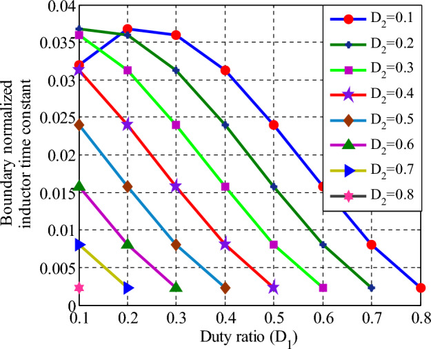
The variation of time constant τB corresponding to duty ratio.
Small-signal modeling
A comprehensive presentation of the converter's small-signal analysis is available in26. Typically, the state variables consist of a (, ) and a perturbation (,). The state-space equations and transfer functions are provided in Eqs. (18–26).
| 18 |
The small-signal model is expressed as in (19)
| 19 |
The suggested converter's average model is structured according to (20)–(22), where in , , and represent the control variable vector, system output vector, and state variable vector respectively.
| 20 |
| 21 |
| 22 |
The control transfer function for the recommended configuration is in (23)–(25)
| 23 |
| 24 |
| 25 |
| 26 |
The frequency response of the suggested converter is tested using Eq. (26), and it is shown in Fig. 5. The bode plot shows that the gain margin is infinite dB, and the phase margin is 155°.
Figure 5.
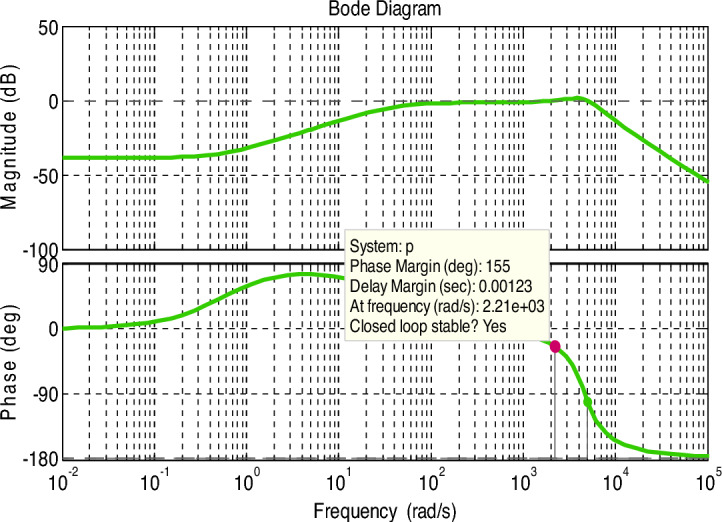
Bode plot response.
Performance analysis of the suggested converter
Effect of parasitic
Figure 6 illustrates the converter configuration considering parasitic resistances. Where RDS is the on-state resistance of the switch, rD1, rD2, and rD3 are the forward resistance of the diodes D1-3, respectively. rL1-2 is the ESR of the inductor L1-L2. The output voltage with parasitic elements expression from the modes of operation is as follows27.
Figure 6.
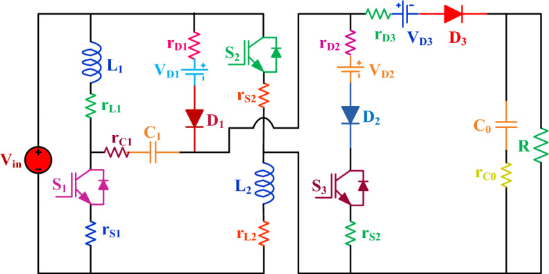
The proposed converter with parasitic.
- Mode I:
- Mode 2:
- Mode 3:
-
During the operation within the time interval of (1-D1-D2) Ts, all power switches are deactivated. Equations (32) and (33) provide the expressions for the Ico, and VL1, in this mode.
32
where.33 34 By employing the principle of volt-second balance to either inductor L1 or L2, Eq. (35) can be derived.35 The gain of the proposed converter is tested using Eq. (35) at ideal and different values of load resistances. The corresponding plot is illustrated in Fig. 7.
Figure 7.
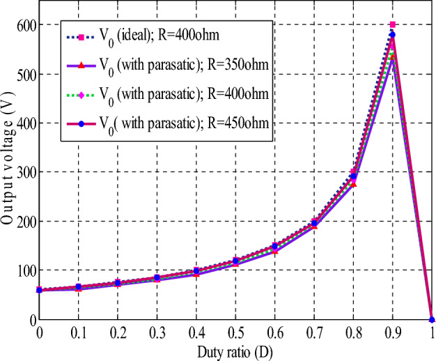
Change in the output voltage concerning the duty ratio, considering parasitic effects.
Power loss analysis
The input power is given in (36).
| 36 |
| 37 |
From Eqs. (36) and (37), the expression of efficiency for the proposed converter is given (38)
| 38 |
Based on the switching losses (Psw), the output power of the proposed configuration is as given in (40). Using (36), (37), and (40), the efficiency is as given (43).
| 39 |
| 40 |
The inductor loss
| 41 |
The capacitor loss
| 42 |
| 43 |
Calculation of voltage stress
The voltage stress on the power devices in the proposed configuration is in the (44) and is based on27.
| 44 |
Converter parameters design
The design and selection of the converter are followed in27. The components and specifications of the components are listed in Table 1.
Table 1.
Test system specifications.
| Parameter | Simulation |
|---|---|
| Input voltage (V) | 30 V |
| Output voltage (V0) | 400 V |
| Output currents (I0) | 1.25 A |
| Switching frequency (f) | 50 kHz |
| Inductors (L) | 0.5 mH |
| Capacitor (C) | 300 uF |
The Inductance calculation is
| 45 |
The inductor ripple current is calculated as (44)
| 46 |
The determination of the capacitance value using below Eq. (47).
| 47 |
| 48 |
The ripple voltage (Vr) is 1% V0.
Comparative analysis
A comparative evaluation of the proposed converter in relation to other advanced converters is presented in Table 2 and visually depicted in Fig. 8.
Table 2.
Comparison with existing high gain converters.
| Ref. no. | Switches | Diodes | L | C | Voltage stress Vstress_max | Switching scheme | Operating range of duty ratio for high gain | Voltage gain |
|---|---|---|---|---|---|---|---|---|
| 4 | 2 | 4 | 3 | 5 | PWM | Extreme (D > 0.5) | ||
| 5 | 1 | 3 | 2 | 3 | PWM | Extreme (D > 0.7) | ||
| 6 | 1 | 3 | 2 | 4 | PWM | Extreme (D > 0.7) | ||
| 11 | 1 | 3 | 2 | 3 | PWM | Extreme (D > 0.7) | ||
| 19 | 1 | 5 | 2 | 5 | PWM | Limited (D < 0.5) | ||
| 20 | 1 | 3 | 3 | 5 | PWM | Limited (D < 0.5) | ||
| 21 | 2 | 3 | 2 | 4 | PWM | Limited (D < 0.5) | ||
| 23 | 2 | 3 | 2 | 3 | PWM | Extreme (D > 0.7) | ||
| 24 | 3 | 3 | 2 | 2 | Time-sharing | Without extreme (D1 + D2 > 0.7) | ||
| Pro | 3 | 3 | 2 | 2 | Time-sharing | Without extreme (D1 + D2 > 0.7) |
Figure 8.
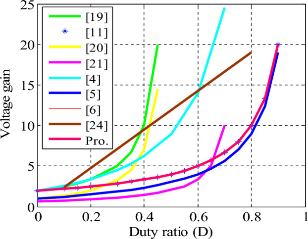
Voltage gain comparison.
Results and discussions
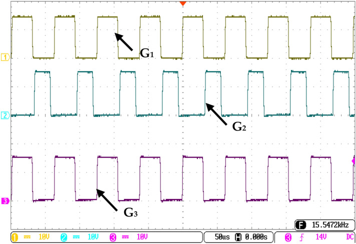
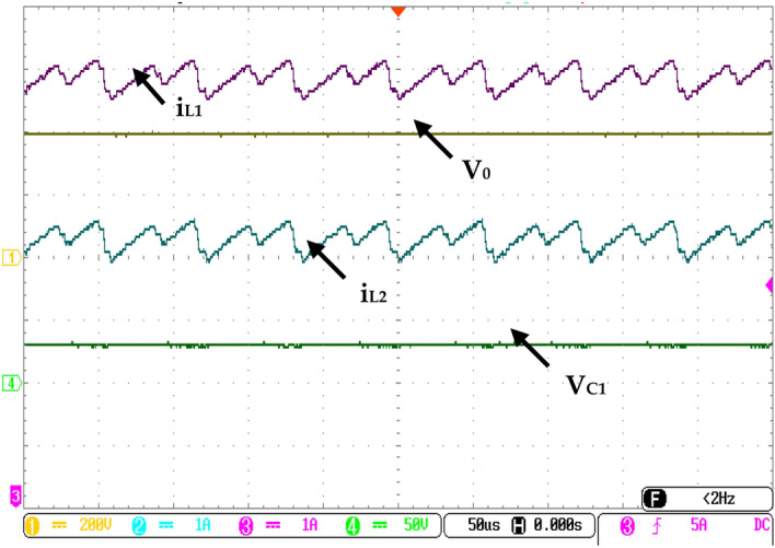
The proposed configuration is simulated with an input voltage of 30 V, a switching frequency of 50 kHz, and duty ratios assigned as D (D1 = 50%, D2 = 35%). Detailed parameter information can be found in Table 1. Figure 9a illustrates the switching control gate pulses (G1–G3) utilized in the proposed converter for controlling the switches (S1–S3) respectively. Figure 9b shows the output voltage (V0) is near 398 V, inductor current (iL1 and iL2) is 8.25A, and capacitor voltage (VC1) is charged to 30 V. The simulated output voltage is cross-validated with the derived expression in Eq. (6). In Mode-1, both inductors are energized in parallel up to d = 50%, and in Mode-2 also, L1 and L2 are energized with d = 35%, facilitated through the active switches S1, S2, and S3 respectively. The corresponding inductor currents are depicted in Fig. 9b.
Figure 9.
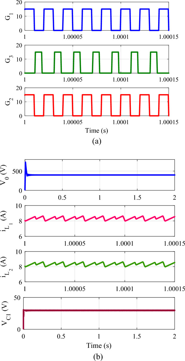
Simulation results: (a) Gate pulses of switches (G1, G3, and G2) and (b) V0, iL1, iL2, and VC1.
Additionally, the voltage across capacitor C1 is shown. Notably, VC1 equals the input voltage. Figure 10 presents the insulation against voltage stress on the power semiconductor switches. A zero voltage across the switch indicates the ON state, while voltage is evident across the switch when it is OFF. Specifically, Fig. 10a illustrates the voltage stress for switches S1, S2, and D1. The magnitude of the voltage across the device (S1, S2, D1) is 200 V and validated with Eq. (44). Figure 10b depicts the voltage stress for switch S3, diode D2, and D3. The maximum voltage stress on the device (S3, D2, D3) aligns with the output voltage i.e. 398 V from the stress results. Furthermore, power loss distribution for switches and diodes is displayed in Fig. 11a, and efficiency with respect to output power is illustrated in Fig. 11b. The practical feasibility of the converter is validated on the laboratory prototype. The test is conducted at VDC = 30 V, D1 = 50%, D2 = 35%, and the switching frequency is 50 kHz. The switching gate pules of the semiconductor devices (S1-S3) are shown in Fig. 12. Figure 13 illustrates the output voltage (V0), current flows through the inductor (iL1 and iL2), and the voltage across the capacitor (VC1) respectively.
Figure 10.
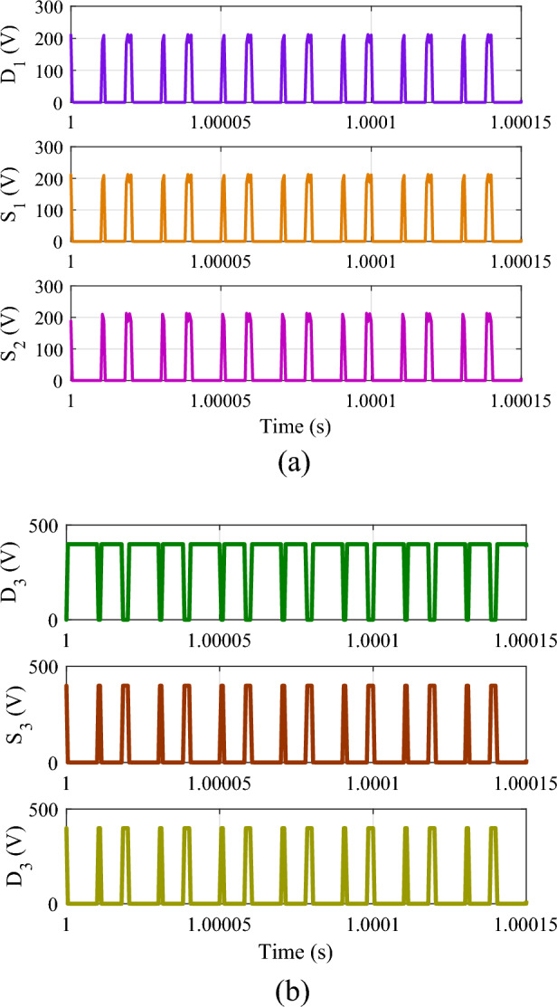
Voltage stress: (a) (D3, S3, and D2) and (b) (D1, S1, and S2).
Figure 11.
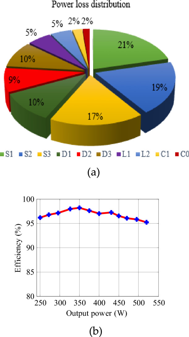
(a) Power loss across each component, (b) efficiency vs output power of converter.
Figure 12.
Experimental gate pules of the switches.
Figure 13.
Experimental results of output voltage, inductor currents, and the voltage across the capacitor.
Conclusion
In this manuscript, introduce a non-isolated high-gain step-up DC–DC converter designed for fuel cell-based electric vehicles. This converter enhances voltage gain without resorting to voltage multiplier units, transformers, or coupled inductors. A key advantage is its streamlined component count. The approach employs a time-sharing mechanism within the configuration, broadening the range of duty cycle operations, thereby boosting converter efficiency and optimizing input source utilization. The proposed converter achieves a remarkable voltage gain of 13.33 times the input voltage while attaining an efficiency of 97.4%. These results demonstrate competitive performance for fuel cell EV applications. In future work, the proposed converter will be tested in a DC microgrid through an inverter, along with a suitable energy management scheme to regulate the load voltage.
Author contributions
Data curation, B.A..; formal analysis, T.K. and T.S.B.; funding acquisition, T.S.B. and S.S.; methodology, B.A and T.K..; project administration, T.S.B. and S.S., resources, B.A., and T.S.B.; supervision, S.S.; writing—original draft, B.A. and T.K. All authors have read and agreed to the published version of the manuscript.
Data availability
The data used to support the findings of this study are included in the article.
Competing interests
The authors declare no competing interests.
Footnotes
Publisher's note
Springer Nature remains neutral with regard to jurisdictional claims in published maps and institutional affiliations.
References
- 1.Nandankar, P. V., Bedekar, P. P. & Dhawas, P. V. Efficient DC–DC converter with optimized switching control: A comprehensive review. Sustain. Energy Technol. Assess.48, 101670 (2021). [Google Scholar]
- 2.Purushothaman, S. K., Sattianadan, D. & Vijayakumar, K. Novel compact design high gain DC–DC step up converter applicable for PV applications. Sustain. Energy Technol. Assess.51, 101720 (2022). [Google Scholar]
- 3.Afkar, M. et al. Commandable areas of a modular converter for DC voltage imbalance mitigation in fuel cell systems. Sustain. Energy Technol. Assess.48, 101664 (2021). [Google Scholar]
- 4.Navamani, J. D. et al. Modified LUO high gain DC–DC converter with minimal capacitor stress for electric vehicle application. IEEE Access9, 122335–122350 (2021). 10.1109/ACCESS.2021.3109273 [DOI] [Google Scholar]
- 5.Saravanan, S. & RameshBabu, N. Analysis and implementation of high step-up DC–DC converter for PV based grid application. Appl. Energy190, 64–72 (2017). 10.1016/j.apenergy.2016.12.094 [DOI] [Google Scholar]
- 6.Pires, V. F., Foito, D. & Silva, J. F. A single switch hybrid DC/DC converter with extended static gain for photovoltaic applications. Electr. Power Syst. Res.146, 228–235 (2017). 10.1016/j.epsr.2017.02.001 [DOI] [Google Scholar]
- 7.Mitra, L. & Rout, U. K. Performance analysis of a new high gain DC–DC converter interfaced with solar photovoltaic module. Renew. Energy Focus19, 63–74 (2017). 10.1016/j.ref.2017.05.001 [DOI] [Google Scholar]
- 8.Kumar, G. G. et al. Switched capacitor–inductor network based ultra-gain DC–DC converter using single switch. IEEE Trans. Industr. Electron.67(12), 10274–10283 (2020). 10.1109/TIE.2019.2962406 [DOI] [Google Scholar]
- 9.Axelrod, B., Berkovich, Y. & Ioinovici, A. Switched-capacitor/switched-inductor structures for getting transformerless hybrid DC–DC PWM converters. IEEE Trans. Circuits Syst. I Regul. Pap.55(2), 687–696 (2008). 10.1109/TCSI.2008.916403 [DOI] [Google Scholar]
- 10.Chung, H. S. H. et al. Development of a switched-capacitor DC–DC converter with bidirectional power flow. IEEE Trans. Circuits Syst. I Fundam. Theory Appl.47(9), 1383–1389 (2000). 10.1109/81.883334 [DOI] [Google Scholar]
- 11.Prudente, M. et al. Voltage multiplier cells applied to non-isolated DC–DC converters. IEEE Trans. Power Electron.23(2), 871–887 (2008). 10.1109/TPEL.2007.915762 [DOI] [Google Scholar]
- 12.Lin, T.-J., Chen, J.-F. & Hsieh, Y.-P. A novel high step-up DC–DC converter with coupled-inductor. In 2013 1st International Future Energy Electronics Conference (IFEEC), 777–782 (2013).
- 13.Zhu, M. U. & Luo, F. L. Series SEPIC implementing voltage-lift technique for DC–DC power conversion. IET Power Electron.1(1), 109–121 (2008). 10.1049/iet-pel:20060494 [DOI] [Google Scholar]
- 14.Raj, A., Arya, S. R. & Gupta, J. Solar PV array-based DC–DC converter with MPPT for low power applications. Renew. Energy Focus34, 109–119 (2020). 10.1016/j.ref.2020.05.003 [DOI] [Google Scholar]
- 15.Saadatizadeh, Z. et al. Expandable interleaved high voltage gain boost DC–DC converter with low switching stress. Int. J. Circuit Theory Appl.47(5), 782–804 (2019). 10.1002/cta.2608 [DOI] [Google Scholar]
- 16.Baddipadiga, B. P., Prabhala, V. A. & Ferdowsi, M. A family of high-voltage-gain DC–DC converters based on a generalized structure. IEEE Trans. Power Electron.33(10), 8399–8411 (2017). 10.1109/TPEL.2017.2777451 [DOI] [Google Scholar]
- 17.Kumar, S. et al. Artificial intelligence power controller of fuel cell based DC nanogrid. Renew. Energy Focus34, 120–128 (2020). 10.1016/j.ref.2020.05.004 [DOI] [Google Scholar]
- 18.Hu, X. & Gong, C. A high gain input-parallel output-series DC/DC converter with dual coupled inductors. IEEE Trans. Power Electron.30(3), 1306–1317 (2014). 10.1109/TPEL.2014.2315613 [DOI] [Google Scholar]
- 19.Zhang, Y. et al. A wide input-voltage range quasi-Z-source boost DC–DC converter with high-voltage gain for fuel cell vehicles. IEEE Trans. Ind. Electron.65(6), 5201–5212 (2017). 10.1109/TIE.2017.2745449 [DOI] [Google Scholar]
- 20.Shindo, Y., Yamanaka, M. & Koizumi, H. Z-source DC–DC converter with cascade switched capacitor. In IECON 2011—37th Annual Conference of the IEEE Industrial Electronics Society, 1665–1670 (2011).
- 21.Zhang, Y. et al. Wide input-voltage range boost three-level DC–DC converter with quasi-Z source for fuel cell vehicles. IEEE Trans. Power Electron.32(9), 6728–6738 (2016). 10.1109/TPEL.2016.2625327 [DOI] [Google Scholar]
- 22.Hu, X. & Gong, C. A high voltage gain DC–DC converter integrating coupled-inductor and diode–capacitor techniques. IEEE Trans. Power Electron.29(2), 789–800 (2013). [Google Scholar]
- 23.Yang, L. S., Liang, T. J. & Chen, J. F. Transformerless DC–DC converters with high step-up voltage gain. IEEE Trans. Ind. Electron.56(8), 3144–3152 (2009). 10.1109/TIE.2009.2022512 [DOI] [Google Scholar]
- 24.Bhaskar, M. S. et al. High gain transformer-less double-duty-triple-mode DC/DC converter for DC microgrid. IEEE Access7, 36353–36370 (2019). 10.1109/ACCESS.2019.2902440 [DOI] [Google Scholar]
- 25.Lee, S. S. et al. Two-inductor non-isolated DC–DC converter with high step-up voltage gain. J. Power Electron.19(5), 1069–1073 (2019). [Google Scholar]
- 26.Ramanarayanan, V. Course Material on Switched Mode Power Conversion, 2nd ed (2007).
- 27.Kazimierczuk, M. K. Pulse-Width Modulated DC–DC Power Converters 2nd edn. (Wiley, 2013). [Google Scholar]
Associated Data
This section collects any data citations, data availability statements, or supplementary materials included in this article.
Data Availability Statement
The data used to support the findings of this study are included in the article.