Abstract
Vanadium dioxide has attracted much interest due to the drastic change of the electrical and optical properties it exhibits during the transition from the semiconductor state to the metallic state, which takes place at a critical temperature of about 68 °C. Much study has been especially devoted to developing advanced fabrication methodologies to improve the performance of VO2 thin films for phase-change applications in optical devices. Films structural and morphological characterisation is normally performed with expensive and time consuming equipment, as x-ray diffractometers, electron microscopes and atomic force microscopes. Here we propose a purely optical approach which combines Polarized Raman Mapping and Phase-Transition by Continuous Wave Optical Excitation (PTCWE) to acquire through two simple measurements structural, morphological and thermal behaviour information on polycrystalline VO2 thin films. The combination of the two techniques allows to reconstruct a complete picture of the properties of the films in a fast and effective manner, and also to unveil an interesting stepped appearance of the hysteresis cycles probably induced by the progressive stabilization of rutile metallic domains embedded in the semiconducting monoclinic matrix.
Keywords: VO2 thin films, Phase transition, Polarized Raman, Continuous wave excitation
Subject terms: Applied optics, Materials for optics
Introduction
Vanadium dioxide (VO2) has been deeply investigated since 1959 when Morin reported for the first time the evidence of the semiconductor-metallic phase transition (SMT)1. The interest in VO2 is because of the drastic change of the electrical properties (electrical conductivity may change up to 5 orders of magnitude2), as well as of the optical properties during the SMT (first-order phase transition) from the semiconductor state (monoclinic M1 crystallographic structure), to the metallic state (rutile R structure). The phase change takes place at the critical temperature of about Tc ≅ 68 °C with a very narrow hysteresis for single crystal VO2 films; at high temperatures (T > Tc) vanadium dioxide exhibits metallic properties, showing a high electrical conductivity, and low transparency in the infrared spectral range, while at low temperatures (T < Tc) VO2 behaves as a semiconductor, showing a relatively high transparency in the infrared spectral range and a large resistivity3.
Several studies have reported on different VO2 morphologies using various fabrication methods and accompanied by performance improvement. Additionally, a deep understanding of the mechanisms behind phase-transition behaviors is beneficial to better modulating performance in VO2 materials4. In fact, the mechanism of this transition is still under discussion and may involve the formation of intermediate phases such as triclinic VO25.
Upon the phase transition at Tc, many physical parameters of VO2 (e.g., transmittance, resistivity) abruptly change with a characteristic hysteresis loop. In VO2 thin films an enlargement of the hysteresis loop, due to the presence of a great number of size-distributed nanocrystals, is observed. This larger hysteresis loop can be thought as the superimposition of many elementary cycles provided by each nanocrystal6.
Recently, reproducible hysteresis cycles exhibiting a width inversely proportional to the VO2 crystallite size film have been reported7. In ref7 the infrared radiometric measurements performed upon phase transition on the different VO2 thin films deposited on a sapphire substrate, in both the SWIR range (2.5–5 µm) and LWIR range (8–12 µm), are presented; a comparison with x-ray diffraction (XRD) analysis is also presented and discussed. In general, the width of the transition upon heating is slightly sharper than the corresponding width during the cooling cycles, as explained in terms of the size distribution and of the different strain contribution in the two cycles. The main results indicate a good agreement between XRD and optical analysis demonstrating that the structural transition from monoclinic to tetragonal (rutile) phases is the dominating mechanism for controlling the global properties of the SMT transition.
In the case of thin films for applications to optical devices, a lot of work has been done about the infrared properties of VO2 films8–11, showing many interesting effects, such as the large tunability of the spectral emittance of VO2 in thermal-controlled devices. However, a fast and effective understanding of the details of polycrystalline structures and the boundaries between the crystal areas for performance optimization is still difficult, the analysis being generally based on high cost and low throughput techniques, like XRD12, atomic force microscopy (AFM)13, ultrasonic surface wave14 or electron microscopy15.
Here we propose a purely optical approach which combines Polarized Raman Mapping and Phase-Transition by Continuous Wave optical excitation to acquire both morphological and thermal behaviour information on vanadium dioxide polycrystalline thin films for phase-change applications.
Raman spectroscopy is based on inelastic scattering of light interacting with matter, and is largely applied to analyse physico-chemical properties of materials by identification of their characteristic vibrations. Thus, it is a natural and powerful tool to study phonons and phase transitions in crystals. Recently, it has been used to accurately identify symmetries and values of Raman tensor elements for all the phonon modes of VO216,17 and for other VO2 polymorphs18. In this case, the possibility to control the polarization of the excitation laser is particularly impactful, since Raman scattering is based on the coupling between the electric field of the incident light and the charge distribution of the target material. Consequently, for anisotropic single crystals, Raman peak intensities are significantly dependent on the relative orientation between light polarization and sample axes19. This dependence has been already exploited to realize angle-resolved measurements and orientational maps of polycrystalline materials20 and VO2 films with micrometric crystal domains21–24. Here we leverage Polarized Raman micro-spectroscopy to collect large images of the surface of VO2 thin films with different thickness getting fast morphological information on the size, distribution and different orientation of the crystal grains. At the same time, Raman analysis is locally used to study also the thermal behaviour of the films, by following the reversible SMT evidenced by the disappearing and reappearing of the vibrational features associated to the semiconducting phase upon controlled external heating13,17,25–27. In this regard, to overcome the limitations of the technique with respect to temperature resolution, we also developed a methodology which relies on the possibility to register the variation of the film optical properties directly associated to the local SMT induced by progressive heating caused by the same exciting laser used to test the film's permittivity. The combination of the two techniques not only allows to reconstruct a complete picture of the properties of the samples, in a fast and effective manner, for comparison and optimization purposes, but also to unveil an interesting stepped structure of the hysteresis cycles assigned to the progressive stabilization of rutile metallic domains embedded in the semiconducting, not yet transformed, monoclinic matrix.
Materials and methods
Samples fabrication
Vanadium dioxide thin films were realized by pulsed laser deposition (PLD) onto 0.5 mm-thick, 2 cm × 2 cm polycrystalline polished sapphire substrates. The PLD system employs a Q-switched Nd:YAG laser (Quantel mod. YG78C20, λ = 355 nm, pulse width 6 ns, pulse energy 60 mJ). More details are reported in11. The VO2 target was a 2-inch diameter, 0.25-inch-thick disk purchased by Testbourne Ltd, UK, (purity 99.99%). Prior to the deposition, each substrate was cleaned in an ultrasonic bath with acetone, subsequently rinsed with isopropanol and then dried with compressed air. Deposition temperature was stably fixed through a vacuum electrical heater equipped with a PID temperature controller, while oxygen pressure within the deposition chamber was controlled through an electromechanical valve. Two VO2 films with different thickness, 340 nm (sample A) and 410 nm (sample B), were deposited at the same deposition conditions (550 °C and 10–2 mbar oxygen pressure). Films thickness was assessed by Rutherford backscattering spectrometry (RBS)11. As an example, Fig. S1 presents the SEM cross section of a VO2 film with a measured thickness of about 690 nm11.
Raman analysis
Single Raman spectra have been obtained with a DXR2xi Thermo Fisher Scientific Raman Imaging Microscope, by exciting the samples at 532 nm with 5 mW laser power and a 50 × objective. The data acquisition was performed in backscattering geometry summing up 200 accumulations each lasting 0.2 s. The temperature-controlled measurements have been performed by using a customized HCP202S Instec hot plate. Each spectrum is acquired after ten minutes of temperature stabilization. Band intensities are calculated by means of Lorentzian fitting of the collected spectra.
Polarized maps have been collected with the same apparatus equipped with filters to select two orthogonal polarizations for the excitation laser beam, named X and Y following the axes of the sample handling stage, and to perform angle-resolved selection of the polarization of the diffused Raman signal. Each point spectrum of the maps, acquired at 6 mW of laser power, resulted from 10 accumulations of 100 ms. A 2 μm step size has been chosen to resolve the polycrystalline structure of the films.
Phase-transition by continuous wave optical excitation
A pump-probe experiment is realized by a Coherent MIRA-VERDI laser group, operating in continuous wave (CW) at central wavelengths of 830 nm and, alternatively, the only VERDI laser operating in CW at 532 nm, as an optical pump signal. The optical beam is expanded and collimated by a telescope and impinges normally with a spot size of 4.7 mm onto the VO2 film. The flux of the pump laser (Power/Spot Size) is varied by controlling the average power thanks to a polarizing beam splitter preceded by a rotating half-waveplate. To monitoring the phase transition, a laser diode (PicoQuant), operating in pulsed regime (50 ps pulse width, 1 MHz repetition rate of, 5 µW average power) at a central wavelength of 1310 nm is exploited to produce the probe signal. The 1310 nm wavelength has been selected because technologically relevant for telecom applications. The signal is directed by means of a multimode fiber and a collimating lens to the VO2 film with an angle of 45°, with a spot size smaller than that of the pump beam. The transmitted and reflected signals from the VO2 sample are collected in two multimodal optical fibers by coupler systems and detected by two InGaAs (ID200 ID Quantique) single photon detectors, operating in gated mode synchronized with the laser diode frequency.
Results and discussion
Single point unpolarised Raman spectra have been first acquired at room temperature on the thicker VO2 film (sample B) to identify the VO2 characteristic vibrational features. Figure 1 reports the obtained data in the region between 50 and 1000 cm-1. All the Raman active modes indicated in Fig. 1 have been already reported and studied in the literature, with detailed symmetry assignments16–18.
Figure 1.
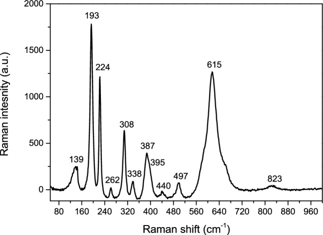
Unpolarised Raman spectrum obtained from the thickest VO2 layer (sample B), and identification of the main vibrational peaks.
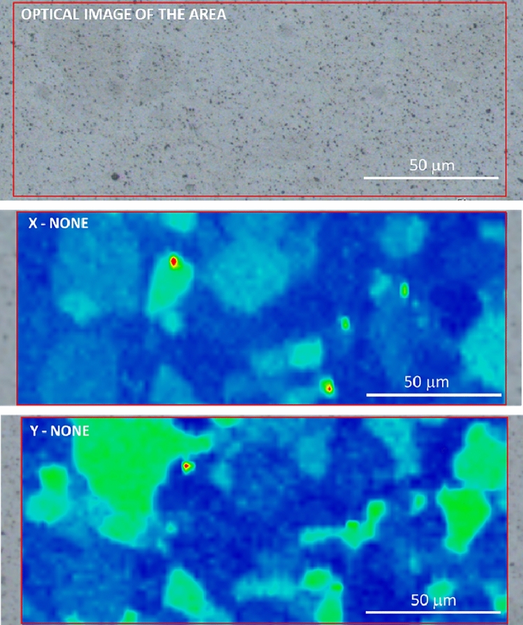
Raman maps have been then collected on the films by controlling the polarization of the excitation laser beam to investigate the presence of differently oriented domains on a quite large scale. Figure 2 shows, from top to bottom, the bare optical image of the surface and two different 100 × 150 μm2 spectral maps obtained from sample B. The boundaries of the analysed area are identified by the red rectangle. The two maps are collected on the very same region with orthogonal X and Y polarized laser excitation (with no polarization on the detectors, i.e., X-none and Y-none in standard Porto notation28), respectively, and are represented as a chemigram based on the restricted spectral region between 160 and 240 cm-1, still containing, point by point, all the information on the entire measurement spectral range. The resulting colour contrast thus refers to the relative intensity of the two peaks (see Fig. 1) located at about 224 cm−1, which is invariant under laser polarization variation, and about 193 cm−1, whose intensity varies with the relative orientation between light polarization and crystal axes. In fact, the maps allow to clearly evidence the appearance of “Off” (blue coloured) and “On” (green coloured) domains depending on the specific orientation of the grains with respect to the X and Y axis of the sample handling stage of the Raman microscope. Hence, the polarized Raman imaging appears to be particularly interesting for fast large area characterization of the films, given that each map carries a lot of spatial, dimensional and orientational information.
Figure 2.
Appearance of “Off” (blue coloured) and “On” (green coloured) domains in large area polarized Raman maps of the thickest VO2 thin film (sample B). The top panel represents the optical image of the analysed area. The two maps are collected on the very same region with X and Y polarized laser excitation and no polarization on the detection (X-none and Y-none), respectively, and are represented as a chemigram referred to the spectral region between 160 and 240 cm−1. The scale marker is the same for the three images.
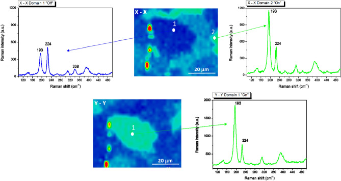
Figure 3 better illustrates and clarifies the crystal orientation dependence of the polarized Raman maps by focusing on a smaller area. The two maps reported in the Figure are collected on the very same region with X (top panel) and Y (bottom panel) polarized laser excitation, by also controlling the polarization of the diffused photons (X and Y, respectively). By following the Porto notation, the images are named X-X and Y-Y28. Also in this case, the maps are represented as a chemigram referred to the spectral region between 160 and 240 cm−1, so that the contrast appears inverted in the two cases: the spectrum collected on the central domain, indicated as 1 in the X-X map and appearing “Off” (blue) in the image, is reported on the left. It presents a low intensity of the peak at about 193 cm−1, and the appearance of a peak at about 338 cm-1. The spectrum collected on the lateral domain, indicated as 2 in the X-X map and appearing “On” (green) in the image, is reported on the right. It presents a high intensity of the peak at about 193 cm−1, but no signal at 338 cm-1. However, the central domain 1 turns “On” when inverting the polarization, in the Y–Y image, because the two spectral features at 193 and 338 cm−1 correspond to orthogonal vibrations of the V atoms along and perpendicular to the c-axis of the VO2 crystal, respectively29. In fact, Raman peak intensities of these two modes are significantly dependent on the relative orientation between the polarization of the excitation light and the direction of the vibration, and this is the reason why they are used here to highlight the separation between differently oriented crystallites.
Figure 3.
Crystal grain orientation dependence of the Polarized Raman maps. The maps are collected on the very same region by changing the polarization of the excitation laser and controlling the polarization at the detector. Top Panel: the spectrum collected on the central domain, named 1 in the X-X map and appearing “Off” (blue), is reported on the left. The spectrum collected on the lateral domain, named 2 and appearing “On” (green), is reported on the right. Bottom Panel: the central domain 1 turns “On” when inverting the polarization, in the Y–Y image.
Actually, the larger maps reported in Fig. 2 demonstrates that several domains appear with a plethora of different orientations, going from the perfect match of the crystallite axes with the polarization of the laser beam, corresponding to the perfectly “On” grain, to the perfectly “Off” state associated to the minimum intensity of the peak at 193 cm-1. Moreover, the larger ones are presumably composed by smaller sub-grains with similar but slightly different orientations. A complete study of the specific orientation of each grain would require a full determination of all Raman tensor elements, but even the partial information obtainable by a single map acquired with a specific laser light polarization can result extremely useful to characterize the films for fabrication process optimisation purposes. As an example, Fig. 4 compares the X-None Raman maps obtained on the two studied films. Given that the scale bar on the maps is the same, the images allow to investigate the grain size dependence on film thickness, estimating the specific ranges of linear domain dimension, passing from 10–30 μm for the thinner sample named A (340 nm) to 20—50 μm for the thicker sample named B (410 nm). The dimensional increase can be better visualized by approximating the area of the domains with circles, so to define the distribution of the mean radii as a function of the film thickness, as reported in Fig. 4c. Further evidence of the Polarized Raman mapping ability to estimate the grain size dependence on the film thickness is given by the data reported in Fig. S2, which compares the X-None Raman images of films with a larger thickness difference.
Figure 4.
Grain size dependence on film thickness analysed by X-None Raman mapping: (a) sample A (340 nm-thick); (b) sample B (410 nm-thick); (c) histograms of the radius distribution of the domains approximated as circles. The scale bar on the maps is the same.
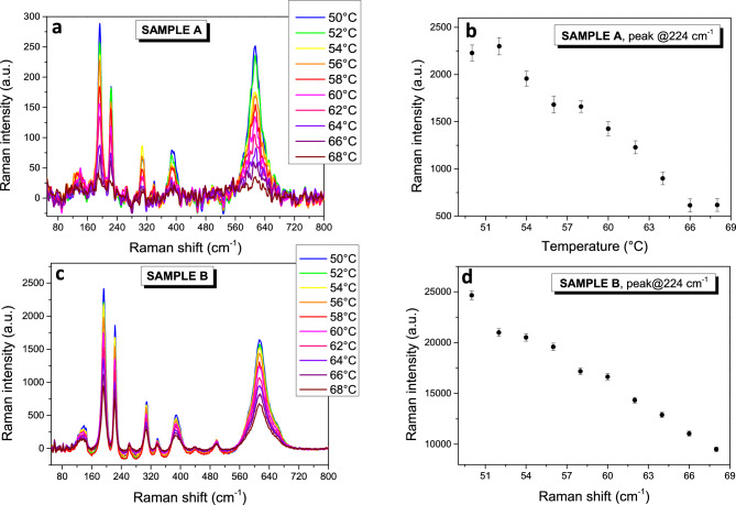
Moreover, once identified a single crystallite, Raman spectroscopy allows to locally study the SMT transition. Figure 5 presents the unpolarised data collected on both samples by varying the temperature through the critical value. Figures 5a,c show, respectively, the full spectra obtained on the two films at different temperatures controlled by means of a thermal stage placed under the samples (each spectrum is acquired after ten minutes of temperature stabilization). The transition to the metallic phase is clearly associated to the progressive disappearance of the vibrational bands. Interestingly, when reporting the intensity of the Raman features as a function of the local temperature, a stepped behaviour appears for both films, as shown in Figs. 5b,d for the band at about 224 cm−1, used above as a reference spectral signature, independent form the polarization of the excitation laser, to obtain the polarized Raman maps in Figs. 2, 3 and 4.
Figure 5.
Raman analysis of the SMT transition. (a) Full spectra acquired on sample A (340 nm); (b) intensity of the band located at about 224 cm−1 as a function of the temperature for sample film A; (c) Full spectra acquired on sample B (410 nm); (d) intensity of the band located at about 224 cm-1 as a function of the temperature for sample B.
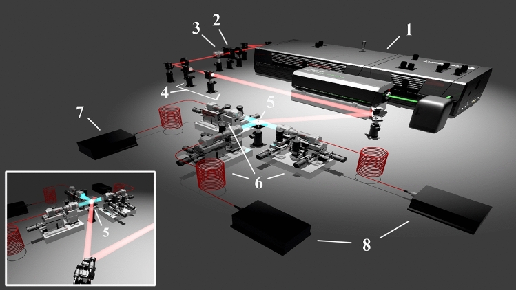
To shed more light on this transition behaviour we developed and tested a pump-probe methodology which is based on the possibility to monitor the variation of the film optical properties following the progressive heating caused by the impinging laser beam. The schematic of the PTCWE employed setup is reported in Fig. 6: an optical input signal is generated by a CW laser (1). The optical beam, which acts as the pump, is expanded and collimated by a telescope (4) and normally impinges on the VO2 film (5) (see the inset of the Figure), which, absorbing the laser radiation, heats up. This causes a local increase of the film temperature. Due to the continuous wave regime, a steady state condition is established, so that the heat generated in the VO2 film by the optical input is dissipated through the substrate by heat conduction, and to the air by heat convection. The flux of the pump laser (Power/Spot Size), used to increase the sample temperature, is varied by controlling the average power thanks to a polarizing beam splitter (3) preceded by a rotating half-waveplate (2). To monitoring the phase transition, a laser diode operating in pulsed regime is exploited to produce the probe signal (7). The signal is directed by means of a multimode fiber and a collimating lens to the VO2 film with an angle of 45°, with a spot size smaller than that of the pump beam. The transmitted and reflected signal from the sample are collected in two multimodal optical fibers by coupler systems (6) and detected by two single photon detectors (8).
Figure 6.
Experimental setup of the experiment: (1) pump laser (Coherent Mira 900); (2) half-waveplate; (3) polarizing beam splitter; (4) telescope; (5) sample; (6) coupling units (7) probe laser (PicoQuant LDH-P–C-1310NM); (8) InGaAs single photon detectors.
The heating of the VO2 film, due to the CW optical illumination, depends on its permittivity, but a change in the temperature in turn modifies the permittivity and the amount of incident optical energy that is converted to heat. This behaviour influences then the reflectivity of the sample, which can be monitored over time allowing to highlight these interesting dynamics30. By using the effective medium theory, at intermediate temperature, corresponding to intermediate power of the pump laser, the permittivity of VO2 could be described by the ratio between the fraction of the material existing in the metallic phase, typical of high temperature regime, and the one that remains in the insulator phase with a monoclinic structure.
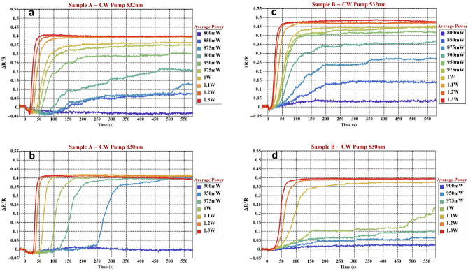
Figure 7 shows the relative reflection change ΔR/R over time of the two VO2 samples induced by optical CW excitation at various average powers. In particular, Figs. 7a,b report, respectively, the behaviour of sample A at 532 nm and 830 nm excitation, while Figs. 7c,d show the analogous data referred to sample B. We observe that for a pump excitation wavelength at 532 nm, at low (800 mW) and high (above 1.1 W) optical flux, the reflection changes as expected for a temperature induced phase transition, while at intermediate optical power densities, for both samples the curves exhibit a clear stepwise behaviour. A similar but less gradual trend can be appreciated when exciting at 830 nm, with different optical flux relevant ranges due to the different absorption of the VO2 sample. We hypothesize that the revealed stepwise behaviour is due to the opposite effects of heating induced by the laser, and cooling due to the increased reflectivity associated to the transition to the metallic phase, so that it can be ascribed to the progressive stabilization of rutile metallic domains embedded in the semiconducting (i.e., not yet transformed) monoclinic matrix. The appearance of the steps, which is also highlighted at lower temperature resolution, and with a slower dynamic, by the Raman measurements (Figs. 5b,d) substantially corresponding to the intermediate excitation regime of the reflectivity measurements of Fig. 7, seems to be a general trend, which was also revealed for photoluminescence properties of similar VO2 thin films31.
Figure 7.
Temporal evolution of the relative reflection change ΔR/R induced by optical CW excitation for various average powers and probed by a picosecond diode laser at 1310 nm. (a) sample A, excitation at 532 nm; (b) sample A, excitation at 830 nm; (c) sample B, excitation at 532 nm; (d) sample B, excitation at 830 nm. In all cases, at t = 0, the pump laser is turned on.
Conclusions
In this paper we have proposed a purely optical analysis of VO2 polycrystalline thin films realized by Pulsed Laser Deposition, performed by combining Polarized Raman Mapping and Phase-Transition by Continuous Wave Optical Excitation. Structural, morphological and thermal behaviour information are obtained, helping for the study of thin film phase-change materials for practical optical applications.
The Polarized Raman Mapping allows to clearly evidence the appearance of “Off” and “On” domains depending on the specific orientation of the grains with respect to the polarization of the excitation laser. Hence, the polarized Raman imaging appears to be particularly interesting for fast large area characterization of the films, given that each map carries a lot of spatial, dimensional and orientational information. The phase transition to the metallic phase of VO2 is also clearly evidenced and associated to the progressive disappearance of the vibrational bands with the induced heating. The Raman intensity acquired in single point measurements shows a stepped profile as a function of the local temperature. A similar behaviour is uncovered in the optical reflection change ΔR/R induced by optical CW excitation at an intermediate range of power during a controlled PTCWE experiment. This trend could be attributed to the simultaneous presence, at intermediate temperatures, of both the metallic and insulator phases in polycrystalline VO2 thin films during the progressive stabilization of rutile metallic domains.
Supplementary Information
Author contributions
V.M, F.A.B, R.L, T.C, R.M, C.S and G.M. designed the study and analysed the data. R.M. and F.V.L. fabricated the samples. V.M. performed the Raman experiments. F.A.B, R.F, D.D. and R.K. performed the PTCWE experiments. V.M, F.A.B, R.L, T.C, R.M, C.S and G.M. wrote the manuscript and participated in manuscript revisions. R.L, T.C, R.M, C.S and G.M acquired funding. All authors agreed with the content of the manuscript.
Funding
This work has been performed in the framework of PNRM “METEORE” (contract n. N. 564, 21.06.2021) project funded by Italian Ministry of Defense.
Data availability
The datasets used and analysed during the current study available from the corresponding author on reasonable request.
Competing interests
The authors declare no competing interests.
Footnotes
Publisher's note
Springer Nature remains neutral with regard to jurisdictional claims in published maps and institutional affiliations.
These authors contributed equally: V. Mussi, F. A. Bovino, C. Sibilia and G. Mattei.
Supplementary Information
The online version contains supplementary material available at 10.1038/s41598-024-70301-0.
References
- 1.Morin, F. J. Oxides Which Show a Metal-to-Insulator Transition at the Neel Temperature. Phys. Rev. Lett.3, 34–36 (1959). 10.1103/PhysRevLett.3.34 [DOI] [Google Scholar]
- 2.Kucharcsyyk, D. & Niklewski, T. J. Accurate X-ray determination of the lattice parameters and the thermal expansion Coefficients of VO2 near the transition temperature. Appl Cristallogr.12(370), 373 (1979). [Google Scholar]
- 3.Goodenough, J. B. The two components of the crystallographic transition in VO2. J. Solid Chem.3, 490–500 (1971). 10.1016/0022-4596(71)90091-0 [DOI] [Google Scholar]
- 4.Shao, Z., Cao, X., Luo, H. & Jin, P. Recent progress in the phase-transition mechanism and modulation of vanadium dioxide materials. NPG Asia Mater.10, 581–605 (2018). 10.1038/s41427-018-0061-2 [DOI] [Google Scholar]
- 5.Shvets, P., Shabanov, A., Maksimova, K. & Goikhman, A. Micro-Raman mapping of VO2 (T) microcrystals orientation. Vibrat. Spectrosc.118, 103328–103336 (2022). 10.1016/j.vibspec.2021.103328 [DOI] [Google Scholar]
- 6.Shadrin, E. B., Il’inskiì, A. V., Sidorovand, A. I. & Khanin, S. D. Size effects upon phase transitions in vanadium oxide nanocomposites. Phys. Solid State52(11), 2426–2433 (2010). 10.1134/S1063783410110338 [DOI] [Google Scholar]
- 7.Cesca, T. et al. Correlation between in situ structural and optical characterization of the semiconductor-to-metal phase transition of VO2 thin films on sapphire. Nanoscale12, 851–863 (2020). 10.1039/C9NR09024J [DOI] [PubMed] [Google Scholar]
- 8.Li Voti, R., Larciprete, M. C., Leahu, G., Sibilia, C. & Bertolotti, M. Optimization of thermochromic VO2 based structures with tunable thermal emissivity. J. Appl. Phys.112, 034305–034315 (2012). 10.1063/1.4739489 [DOI] [Google Scholar]
- 9.Li Voti, R., Larciprete, M. C., Leahu, G., Sibilia, C. & Bertolotti, M. Optical response of multilayer thermochromic VO2-based structures. J. Nanophoton.6, 061601–061606 (2012). 10.1117/1.JNP.6.061601 [DOI] [Google Scholar]
- 10.Leahu, G., Li Voti, R., Sibilia, C. & Bertolotti, M. Anomalous optical switching and thermal hysteresis during semiconductor-metal phase transition of VO2 films on Si substrate. App. Phys. Lett.103, 231114–231115 (2013). 10.1063/1.4838395 [DOI] [Google Scholar]
- 11.Li Voti, R. et al. Optothermal characterization of vanadium dioxide films by Infrared Thermography. Int. J. Ther. Sci.197, 108832 (2024). 10.1016/j.ijthermalsci.2023.108832 [DOI] [Google Scholar]
- 12.Pandey, A., Dalal, S., Dutta, S. & Dixit, A. Structural characterization of polycrystalline thin films by X-ray diffraction techniques. J. Mater. Sci: Mater. Electron.32, 1341–1368 (2021). [Google Scholar]
- 13.Azhan, N. H., Su, K., Okimura, K., Zaghrioui, M. & Sakai, J. Appearance of large crystalline domains in VO2 films grown on sapphire (001) and their phase transition characteristics. J. Appl. Phys.117, 245314–245317 (2015). 10.1063/1.4923223 [DOI] [Google Scholar]
- 14.Sun, Z., Wu, S., Saini, A. & Fan, Z. Characterizing polycrystalline microstructures by reconstructing grain boundaries and velocity map from ultrasonic surface wave field. Ultrasonics137, 107175 (2024). 10.1016/j.ultras.2023.107175 [DOI] [PubMed] [Google Scholar]
- 15.Adams, B. L., Wright, S. I. & Kunze, K. Orientation Imaging: The Emergence of a New Microscopy. Metall. trans. A24A, 819–831 (1993). 10.1007/BF02656503 [DOI] [Google Scholar]
- 16.Svhilbe, P. Raman scattering in VO2. Phys. B316–317, 600–602 (2002). 10.1016/S0921-4526(02)00584-7 [DOI] [Google Scholar]
- 17.Ureña-Begara, F., Crunteanu, A. & Raskina, J.-P. Raman and XPS characterization of vanadium oxide thin films with Temperature. App. Surf. Sci.403, 717–727 (2017). 10.1016/j.apsusc.2017.01.160 [DOI] [Google Scholar]
- 18.Shvets, P., Dikaya, O., Maksimova, K. & Goikhman, A. A review of Raman spectroscopy of vanadium oxides. J. Raman Spectrosc.50, 1226–1244 (2019). 10.1002/jrs.5616 [DOI] [Google Scholar]
- 19.Xu, B., Mao, N., Zhao, Y., Tong, L. & Zhang, J. Polarized Raman Spectroscopy for Determining Crystallographic Orientation of Low-Dimensional Materials. J. Phys. Chem. Lett.12, 7442–7452 (2021). 10.1021/acs.jpclett.1c01889 [DOI] [PubMed] [Google Scholar]
- 20.Schmid, T., Schäfer, N., Levcenko, S., Rissom, T. & Abou-Ras, D. Orientation-distribution mapping of polycrystalline materials by Raman microspectroscopy. Sci. Rep.5, 18410 (2015). 10.1038/srep18410 [DOI] [PMC free article] [PubMed] [Google Scholar]
- 21.Shvets, P., Shabanov, A., Maksimova, K. & Goikhm, A. Micro-Raman mapping of VO2 (T) microcrystals orientation. Vibrat. Spectrosc.118, 103328–103336 (2022). 10.1016/j.vibspec.2021.103328 [DOI] [Google Scholar]
- 22.Shvets, P., Maksimova, K. & Goikhman, A. Polarized Raman scattering in micrometer-sized crystals of triclinic vanadium dioxide. J. Appl. Phys.129, 055302–055307 (2021). 10.1063/5.0032916 [DOI] [Google Scholar]
- 23.Chen, X.-B. Assignment of the Raman Modes of VO2 in the Monoclinic Insulating Phase. J. Korean Phys. Soc.58(1), 100–104 (2011). 10.3938/jkps.58.100 [DOI] [Google Scholar]
- 24.Zaghrioui, M., Sakai, J., Azhan, N. H., Sub, K. & Okimur, K. Polarized Raman scattering of large crystalline domains in VO2 films on sapphire. Vibrat. Spectr.80, 79–85 (2015). 10.1016/j.vibspec.2015.08.003 [DOI] [Google Scholar]
- 25.Zhang, H. et al. The structural phase transition process of free-standing monoclinic vanadium dioxide micron-sized rods: temperature-dependent Raman study. RSC Adv.5, 83139–83143 (2015). 10.1039/C5RA15947D [DOI] [Google Scholar]
- 26.Zhang, et al. Structural mapping of single-crystal VO2 microrods through metal-to-insulator phase transition. J. Mater. Sci.56, 260–268 (2021). 10.1007/s10853-020-05297-9 [DOI] [Google Scholar]
- 27.Zhang, et al. Size, composition and alignment of VO2 microrod crystals by the reduction of V2O5 thin films, and their optical properties through insulator-metal transitions. J. All Comp.827, 154150 (2020). 10.1016/j.jallcom.2020.154150 [DOI] [Google Scholar]
- 28.Damen, T. C., Porto, S. P. S. & Tell, B. Raman effect in zinc oxide. Phys. Rev.142, 570–574 (1966). 10.1103/PhysRev.142.570 [DOI] [Google Scholar]
- 29.Yuan, X., Zhang, W. & Zhang, P. Hole-lattice coupling and photoinduced insulator-metal transition in VO2. Phys. Rev. B88, 035119–035126 (2013). 10.1103/PhysRevB.88.035119 [DOI] [Google Scholar]
- 30.Chettiar, U. K. & Engheta, N. Modeling vanadium dioxide phase transition due to continuous-wave optical signals. Optics Express23, 445–451 (2015). 10.1364/OE.23.000445 [DOI] [PubMed] [Google Scholar]
- 31.Kalinic, B. et al. Active modulation of Er3+ emission lifetime by VO2 phase-change thin-films. Adv. Photon. Res.10.1002/adpr.202300242 (2023). 10.1002/adpr.202300242 [DOI] [Google Scholar]
Associated Data
This section collects any data citations, data availability statements, or supplementary materials included in this article.
Supplementary Materials
Data Availability Statement
The datasets used and analysed during the current study available from the corresponding author on reasonable request.


