

ABSTRACT
The remarkable electronic properties of monolayer MoTe2 make it a very adaptable material for use in optoelectronic and nano-electronic applications. MoTe2 growth often exhibits intrinsic defects, which significantly influence the material’s characteristics. In this work, we conducted a thorough investigation of the electronic characteristics of intrinsic defects, including point defects, in monolayer MoTe2 using first-principles calculations based on density functional theory (DFT). Our findings indicate that the presence of point defects leads to the formation of n-type properties as the Fermi level situates above the conduction band. Our first-principles density functional theory calculation revealed an appearance of donor level in the band gap close to the conduction band in MoTe2. Our study signifies that the formation energy of a vacancy in a Te atom is lower than that of both a vacancy in a Mo atom and two vacancies in Te atom. This suggests that during the synthesis process, it is more probable for Te atom vacancies to be created. A defect in the pristine monolayer of MoTe2 leads to a slight decrease in the band gap, causing a transition from a direct band gap semiconductor to an indirect band gap semiconductor. The results of our study indicate that the presence of vacancy defects may modify the electronic properties of monolayer MoTe2, suggesting its potential as a new platform for electronic applications. Hence, our analysis offers significant theoretical backing for defect engineering in MoTe2 monolayers and other 2D materials, a critical aspect in the advancement of nanoscale devices with the desired functionality.
KEYWORDS: Transition metal dichalcogenides, DFT, MoTe2, defect control, electronic properties
GRAPHICAL ABSTRACT

IMPACT STATEMENT
The study explores the electronic properties of monolayer MoTe2, revealing intrinsic defects that can enhance its potential for electronic applications and providing theoretical support for defect engineering in 2D materials.
Introduction
Since the successful synthesis of graphene, a single layered honeycomb structure of carbon atoms, by Novoselov et al. in 2004 [1], there has been steady progress in scientific interest in many further two-dimensional (2D) monolayers. Graphene has long been considered the most promising candidate to replace silicon. Nevertheless, the absence of a band gap in graphene limits its potential use in semiconductor devices. Therefore, in addition to graphene, additional single layered systems that have been widely researched include silicene, germanene, stanene, phosphorene, and other single layered transition metal dichalcogenides (MX2, M = transition metal and X = chalcogen) [2–15]. These monolayer systems, characterised by 2D structures, often display distinct features compared to their three-dimensional counterparts. As a result, these systems have become significant topics of investigation in both experimental and theoretical investigations. From an application perspective, 2D semiconducting devices possess a minimal thickness and broad band gaps, making them significant in the fields of optoelectronics, photovoltaics, spintronics, sensors, valleytronics, biomedicine, and efficient catalysis. Layered transition metal dichalcogenides (TMDCs) have attracted significant research attention among the widely studied 2D semiconductors [16–18]. This is primarily owing to their optoelectronic characteristics, including the ability to tune bandgaps and achieve valley polarisation. The investigation of doping and point defects in thin layered TMDCs received renewed attention in recent years. Currently, there is a growing interest in the telluride-based TMDCs compared to other TMDCs materials. This is largely due to their ability to exist in a wide variety of stable structural phases (2 H, 1T, and 1T′) at 300 K [19]. MoTe2 in its bulk form is a kind of semiconductor that has an indirect band gap [20]. However, when the thickness is reduced to a single layer, it undergoes a change and becomes a direct band gap semiconductor with a band gap of 1.10 eV due to the quantum confinement effect [21]. Therefore, monolayer MoTe2 is highly regarded among TMDCs due to its favourable band gap and tunability of its mobility via doping as the maximum mobility of 178.73 cm2/V.s obtained [22,23]. These characteristics highlight the significant potential of this fascinating material. Controlling the atomic structure has great potential for modifying electronic characteristics to create devices and enhance catalytic processes. The physical characteristics of monolayer MoTe2 may be further adjusted by deliberately introducing defects. Hence, a comprehensive comprehension of the influence of vacancy defects on electronic properties is crucial in determining appropriate materials that may be manipulated under certain synthesis and processing circumstances. MoTe2 nanosheets have been synthesised with success in experimentally [24]. It has been observed that these layered compounds can be efficiently dispersed in common solvents and can be formed into films or deposited as individual flakes. This suggests that these materials have the potential to be exfoliated into monolayers. Various polymorphs, such as the trigonal prismatic 2 H phase, the monoclinic 1T’-phase, and the orthorhombic Td-phase, may exist based on the arrangement of Te atoms [25–27]. Research has shown that the 2 H-phase of MoTe2 is more energetically desirable compared to the other two phases [28]. Therefore, our subsequent discussion will concentrate only on the MoTe2-2 H-phase. The process of exfoliating large-area monolayer TMDs has been improved by chemical vapour transport (CVT) and chemical vapour deposition (CVD) [29]. At equilibrium, the potential energy of the system consistently rises in relation to various atomic movements. Using vibrational spectra as a filter can help validate the stability of materials, as the presence of imaginary frequency indicates material instability. Theoretical computations by using first-principles calculations and experimental analysis by using broadband optical pump-probe microscopy have been recently reported on the dynamic stability and phonon transport properties of monolayer MoTe2 [30,31].
This advancement has expanded the range of applications for telluride-based TMDs, including logic transistors, superconductors, and valley optoelectronics [31]. Structural defects are commonly observed in large-scale single-layer materials synthesised under changing growth conditions utilising the CVD or CVT technique. Prior empirical investigations have shown the presence of several defects in the monolayer TMDs, including point defects and boundaries [32,33]. The imperfections have the potential to greatly impact the material’s geometric, mechanical, optical, thermal, and electronic characteristics. Moreover, the intrinsic structural imperfections in metal 2D TMDs provide a promising prospect for manipulating the specific characteristics in novel applications. Over the last several years, there has been a great deal studies, both experimental and theoretical, on the electronic properties of defects in materials such as MoS2, MoSe2, WS2, and others [20,24,29,33–38]. Nevertheless, further investigation of the electronic properties related to intrinsic defects in monolayer MoTe2 is still required.
Understanding the effect of defects is crucial to ensure the dependable functioning of devices. This paper presents a comprehensive analysis of the electronic structure of intrinsic defects, such as point defects and substitutional defects by replacing the Mo atom in monolayer MoTe2. We systematically studied the electronic and structural properties of monolayer MoTe2 with defects by means of first-principles calculations based on density functional theory (DFT). We calculated the defect formation energy of monolayer MoTe2. It is found that the lowest formation energies are 67.296 meV/atom and 15.243 meV/atom for Te vacancy and W substitutional defects. When we create additional Te defects by removing one of the upper Te atoms and one of the lower Te atoms, the formation energy increased to 125.651 meV/atom. Additionally, the substitutions of Mo site with Te and W atoms have the low formation energies comparing with Mo vacancy defect. We thoroughly explained the similarities and differences in the electronic properties of various intrinsic defects. Our results suggest that by replacing the Mo site the direct band gap in pristine monolayer MoTe2 can be retained at the K point while the band gap value is reduced to 0.112 eV by Te substitutional effect. Furthermore, it is shown that all defects studied in this work suggest a promising candidate for n-type material. These defects in monolayer MoTe2 have the potential to enhance the material’s characteristics and provide remarkable functions.
Computational method
In this work, we used 5 × 5 monolayer MoTe2 supercell for Mo and Te vacancy defects and single W and Te substitutions. To avoid interaction between periodic images, the vacuum region of 20 Å is inserted in the out-of-plane direction. All the calculations were performed using the plane-wave based Quantum Espresso PWSCF package [39]. The generalized gradient approximation (GGA) of Perdew–Burke–Ernzerhof (PBE) was used for the exchange-correlation potential [40]. The PBE optimised in-plane lattice constant of 3.557Å for monolayer MoTe2 was used to generate the supercells. The spin-orbit coupling was included using fully relativistic projector-augmented-wave potentials for Mo, Te, and W atoms [41]. The total energy and Hellman-Feynman force thresholds were set to be less than 106 eV and 0.001 Ry/a.u, respectively, in our calculations. The energy cutoffs were set at 60 Rydberg (Ry) for the plane-wave basis and 480 Ry for the charge density. The Brillouin zone was sampled using the Monkhorst-Pack uniform k-grid of 6 × 6 × 1 [42]. A Methfessel-Paxton smearing of 0.005 Ry was adopted in all calculations [43]. The charge density differences were calculated using the following expression,
where (Defected supercell) and (Pristine supercell) are total charge densities for 5 × 5 supercell with Mo and Te vacancy defects and single W and Te substitutions and pristine 5 × 5 supercell, respectively.
Results and discussion
The monolayer 2 H – MoTe2 has a hexagonal crystal structure with a space group (p-3m1), as seen in Figure 1(a). The Mo layer is situated between the two Te layers, creating a sandwich configuration known as Te – Mo – Te. The Mo atom is surrounded by six Te atoms arranged in a trigonal prismatic coordination [44]. Before exploring into intrinsic point defects, it is essential to begin with the pristine MoTe2 monolayer. MoTe2 displays multiple-phase configurations, including 2 H, 1T, and 1T′, which are determined by the arrangement of its layers. The 2 H phase has the highest stability at normal room temperature [45]. Therefore, the subsequent discussion will be limited to the subject of 2 H-MoTe2. The computed lattice constant and bond length between the Mo atom and its nearest neighbour Te atoms are, a = 3.557 Å and d = 2.738 Å, respectively. These values are consistent with the previous experimental [21] and theoretical [46,47] findings. Our GGA calculations yielded a direct band at the K point of 0.935 eV for pristine monolayer MoTe2, which is consistent with other DFT and experimental findings [48,49]. In order to conduct a more comprehensive analysis of the conduction band minimum (CBM) and the valence band maximum (VBM) at the K point, the projected density of states (PDOS) is computed. According to our findings, the VBM and CBM are primarily contributed by Mo 4d and Te 5p states, which undergo a division between their occupied and unoccupied states.
Figure 1.
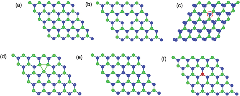
The generation of defect states in monolayer MoTe2. (a) The atomic structure of pristine MoTe2 monolayer, typical vacancy point defects; (b) VMo and (c) VTe , (d) V2Te and (e) the substitution of Mo atom with Te and (f) W atoms, respectively. The green and blue balls represent Mo and Te atoms, respectively. The red dotted circle represents the location of VTe defect.
Defects that are most fundamental and frequently manifest in two-dimensional materials are antisites and vacancies. The five optimised point defective structures discussed in this paper are depicted in Figure 1(b–f). These structures include a single Mo vacancy (VMo), a single Te vacancy (VTe), double Te vacancy (V2Te), and substitutional defects where Te and W atoms replacing Mo atom (TeMo and WMo). We construct 5 × 5MoTe2 supercell to form VMo, VTe , and V2Te defects by removing single Mo atom, single Te atom, and two Te atoms which leads to defect concentrations of 4% for VMo and V2Te defects and 2% for VTe defect are shown in Figure 1(b–d) respectively. These specific intrinsic point defects are routinely seen in synthetic materials.
By utilising argon plasma treatment, it was possible to generate a defect concentration in the basal plane during experiments [50]. In the range of allowed Te chemical potential, Te-vacancy formation energy is lower than that of Mo-vacancy, indicating that Te vacancies may be generated in the experimental growth environments. This is supported by a previous experimental observation [45] in which Te vacancies were readily formed and frequently detected during vacuum annealing. Additionally, it can be easily modified to display either n-type or p-type transfer characteristics [51].
To assess the vacancy formation in a monolayer MoTe2 and a thermodynamically stable defected structure, the formation energy was computed utilising the subsequent formula,
where and show the respective total energies of the supercell with and without a vacancy defect. Also, represents the number of atoms corresponding to element that has been extracted from the pristine structure. The chemical potential of the element is represented by . The formula for calculating the formation energy of substitutional Te and W defects in monolayer MoTe2 is as follows,
where and chemical potentials of Mo and substituted Te (W) atoms. N represents the total number of atoms in the supercell.
The formation energies for five types of defects are listed in Table 1. The MoTe2 monolayer doped with VTe exhibits the least amount of energy required to form vacancy defects. The VMo defect exhibits a significantly greater formation energy in comparison to the VTe and V2Te vacancy defects. This observation becomes easily comprehensible when one considers that producing a Mo vacancy necessitates the disruption of twice as many Mo-Te bonds as is necessary to produce a Te vacancy. By replacing Mo atom with Te and W atoms in monolayer MoTe2, as shown in Figure 1(e,f), the lowest formation energy has been obtained for WMo defect. A persistent difficulty is reducing the significant energy requirements linked to creating active surface regions in 2D monolayers by forming vacancies. As an example, the process of forming a single carbon vacancy in graphene requires an energy of more than 7.5 eV [52]. Similarly, in boron-nitride monolayers, a well-known 2D material, the energy required to produce single nitrogen vacancies (VN) is roughly 4.5 eV, whereas the energy required for the formation of boron vacancies (VB) is around 7 eV [53]. The substantial energy demands associated with the production of flawed 2D materials pose considerable challenges to their extensive use. Nevertheless, MoTe2 monolayers provide a hopeful solution for tackling this obstacle, since they possess vacancies that are more easily reached in terms of energy.
Table 1.
Formation energies and calculated band gap for the structures of pristine and all defective MoTe2 monolayers.
| Structure | Ef (meV/atom) | Eg (eV) |
|---|---|---|
| Pristine | - | 0.935 (direct) |
| VMo | 193.115 | - |
| VTe | 67.296 | 0.711 (indirect) |
| TeMo | 156.007 | 0.113 (direct) |
| WMo | 15.243 | 0.929 (direct) |
| V2Te | 125.651 | 0.754 (indirect) |
Creating atomic defects is a frequent method used to regulate the band gap in monolayer MoTe2, since they are very effective in modifying the band gap. Furthermore, MoTe2 consistently demonstrates ambipolar transfer properties as a result of its narrow band gap and can be readily modified to exhibit n- or p-type transfer [54,55]. Figure 2(a–e) display the energy band structures of defective monolayers of MoTe2, where the red dotted lines illustrate the electronic structure of a defect-free MoTe2 monolayer. Observably, the monolayer MoTe2 without defects is a direct semiconductor with a predicted band gap of 0.935 eV. The valence band maximum (VBM) and conduction band minimum (CBM) are situated at the K point. Upon the creation of VMo, VTe, and V2Te defects, more defect states are created inside the band gap. The introduction of a VTe defect caused a reduction in the band gap by up to 0.711 eV. Nevertheless, the CBM has been relocated to the Γ point, while the VBM remains at the K point. This results in the transformation of the direct band gap semiconductor monolayer MoTe2 into an indirect bandgap semiconductor. Additionally, it is seen that a fresh band emerges underneath the conduction band subsequent to the formation of a vacancy in Te. The presence of a single and double vacancies in MoTe2 monolayer creates localised states inside the band gap of the defect-free material. Similarly, we eliminated two Te atoms in order to generate a double Te vacancy, resulting in the V2Te defect. In order to address this defect, the Te atoms are extracted from the upper and lower atomic layers of the pristine monolayer MoTe2. We get comparable outcomes using the VTe defect. In Figure 2(c), the band gap decreases to 0.754 eV, causing the direct band gap semiconductor behaviour to transition into an indirect band gap semiconductor. The conduction band minimum (CBM) is located at the Γ point, while the valence band maximum (VBM) is located at the K point. We notice that the band gap is slightly higher than the band gap of the VTe defect configuration. This is a result of the presence of defect states inside the energy gap. Hence, the manipulation of various point defects allows for the regulation of the band gap in monolayer MoTe2.
Figure 2.

(a) The electronic band structure of monolayer MoTe2 with VMo defect, (b) VTe defect, (c) V2Te defect, (d) TeMo substitutional defect, and (e) WMo defect. Fermi level is set to zero. The red dotted lines represent electronic structure of defect free monolayer MoTe2.
In the case of a substitutional defect in a monolayer of MoTe2, the band gap is greatly lowered to 0.113 eV. However, as demonstrated in Figure 2(d), the material still maintains its direct semiconductor properties. As represented in Figure 2(e), the presence of a WMo defect in a monolayer of MoTe2 results in a small reduction of the direct band gap value to 0.929 eV. Observably, the valence and conduction bands of monolayer MoTe2 undergo expansion and shift towards higher energy levels in the presence of all five types of defects. Consequently, these defects confer n-type characteristics onto monolayer MoTe2. Recent experimental studies have shown that laser irradiation can be used to create vacancy defects in the MoTe2 monolayer [54,55]. When the MoTe2 monolayer is exposed to laser irradiation in a vacuum, it exhibits characteristics of an n-doped semiconductor. This is because the Fermi level is positioned above the conduction band and does not change with the gate voltage [54]. In addition, MoTe2 crystals can be susceptible to heat damage in the atmosphere due to the relatively low stability of Te atoms. When the temperature reaches 1200 K due to the focused laser, vacancies start to form in the MoTe2 crystal. This happens because the temperature exceeds the threshold of 400 K for producing vacancies in TMDCs [55]. According to previously reported works [54,55], using laser irradiation is a proven method to achieve n-type doping in MoTe2 crystal. Our calculations also have shown the presence of a donor level near the conduction band in MoTe2.
The total density of states (TDOS) and projected density of states (PDOS) are computed, as illustrated in Figures 3 and 4, in order to elucidate the alterations in the electronic structure brought about by the emergence of these five defect types. Figure 3(a) displays the TDOS and PDOS of monolayer MoTe2 with a VMo vacancy. It is clear that the presence of a Mo vacancy in the monolayer MoTe2 significantly alters the density of states. The valence and conduction bands of monolayer MoTe2 have undergone an expansion towards higher energy. The VMo defect produces three peaks near the Fermi level, indicating that the Mo vacancy creates acceptor-like levels in the band gap, resulting in a higher p-type orientation for this defect. The band gap states primarily arise from the p states of the six-nearest neighbour Te atoms surrounding the Mo vacancy, with some contribution from the d states of the Mo atoms. It has been observed that the presence of both single and double Te vacancies leads to a reduction in the band gap due to the emergence of new states near the conduction band minimum. The states primarily arise from the contributions of d molybdenum orbitals, as shown in Figure 3(b,c). Through the formation of vacancies, the electronic properties can be modulated. In addition, the energy levels caused by the absence of Te atoms are higher than the Fermi level, resulting in the formation of levels that act as donors.
Figure 3.

The total and projected density of states for (a) VMo defect, (b) VTe defect, and (c) V2Te defect. The fermi level is set to zero.
Figure 4.

(a) The total and projected density of states for (a) TeMo defect and (b) WTe defect. The fermi level is set to zero.
In Figure 4(a), it is observed that the VBM is primarily influenced by Mo d orbitals, while the CBM is influenced by both Mo d and Te p orbitals in the PDOS of TeMo substitutional defects. When the Mo atom is replaced with Te in the pristine monolayer MoTe2, there is a noticeable alteration in the band gap. It is evident that the electronic properties and chemical activity of the molybdenum telluride monolayer are extremely responsive to substitutional defects. In Figure 4(b), the PDOS for the WMo defect in monolayer MoTe2 is displayed. The dominant formation of band edge states in monolayer MoTe2 is attributed to the d orbitals of Mo in the WMo defect. The contributions are most significant near the energy gap, with the one from Te p orbitals appearing approximately 1 eV below the Fermi level. There appears to be a minor involvement of the W d orbital in the CBM. The defect state is created above the Fermi level. The band gap value of defect-free monolayer MoTe2 is slightly reduced when WMo defect is introduced.
As demonstrated in the previous section, the presence of defects significantly alters the electronic levels of the MoTe2 monolayers. Figure 5(a–e) illustrates the calculated charge density differences for the various defects examined, providing valuable insight into the changes in electron density caused by vacancies and substitutional defects. Figure 5(a–c) demonstrates the absence of charge in the locations where Mo and Te atoms are eliminated, indicating vacancy defects. As a result, there is a significant reorganisation of charge around the vacancies. It is evident from Figure 5(a) that the Te atoms surrounding the Mo vacancy have acquired a higher charge compared to the rest. Two Te atoms surrounding the Mo atom adjacent to the defected region experienced an increase in charge in the case of the VTe and V2Te defects. The charge accumulation is reduced when comparing those Mo vacancy defects. Figure 5(d,e) display the variations in charge density for the substitutional WMo and TeMo defects. Figure 5(d) demonstrates that the substituted W atom provides a greater charge to the surrounding Te atoms compared to the VMo defect. When a Mo atom is replaced with a Te atom, the charge is transferred to the Te atom surrounding the TeMo defect. The Te atom in question receives a charge from the molybdenum atoms and is then substituted by another Te atom, as depicted in Figure 5(e). It has been demonstrated that there is a significant rearrangement of charge surrounding the substitutional Te atom. The electron density around the Te atoms in defected monolayer MoTe2 remains largely unaffected.
Figure 5.

Charge density difference for (a) VMo defect, (b) VTe defect, (c) V2Te defect, (d) WMo defect, and (e) TeMo defect.
Conclusion
Our present study explores the electronic properties of monolayer MoTe2, a material known for its remarkable electronic characteristics, and its potential applications in opto-electronic and nano-electronic fields. Point defects are quite common during the growth of MoTe2 and have a significant impact on its properties. Using first-principles calculations based on DFT, our investigation delves into the electronic properties of these defects, including point defects. Based on our results, it appears that the presence of point defects leads to the development of n-type characteristics as the Fermi-level close to the conduction band near the band edges. Our research offers valuable theoretical support for defect engineering in MoTe2 monolayers and other 2D materials. It plays a crucial role in the development of nanoscale devices with the desired functionality. Our findings suggest that vacancy defects have the potential to significantly impact the electronic properties of monolayer MoTe2, positioning it as an exciting prospect for future electronics applications. Our work emphasises the significance of comprehending how vacancy defects impact electronic properties when selecting materials for manipulation in different synthesis and processing conditions. We found that the formation energy of substitutional defects in monolayer MoTe2 is lower than that of Mo-vacancy. This suggests that Te vacancies could potentially be created in the experimental growth environments. According to our study, MoTe2 monolayers offer a potential solution to decrease the high energy demands associated with creating active surface areas in 2D monolayers through the formation of vacancies.
Our study suggests that by manipulating atomic defects, the band gap in monolayer MoTe2 can be controlled, resulting in adjustments to the valence and conduction bands. Defects in the material have a significant impact on its electronic structure, resulting in the emergence of n-type characteristics. The valence and conduction bands of MoTe2 experience an expansion and move towards higher energy levels. The presence of the VMo defect leads to the appearance of three peaks close to the Fermi level. This suggests that the Mo vacancy generates levels with characteristics similar to acceptors within the band gap. The band gap states mainly originate from the p states of the six-nearest neighbour Te atoms surrounding the Mo vacancy, along with a slight contribution from the d states of the Mo atoms. Substitutional defects have a significant impact on the electronic properties and chemical activity of the MoTe2 monolayer. Examining the charge density differences for the different defects offers valuable insight into how vacancies and substitutional defects affect the electron density.
Acknowledgments
C. Yelgel and Ö. C. Yelgel acknowledge the support from the University of Manchester, the National Graphene Institute, and the School of Physics & Astronomy.
Disclosure statement
No potential conflict of interest was reported by the author(s).
References
- [1].Novoselov KS, Geim AK, V. MS, et al. Electric field in atomically thin carbon films. Science. 2004;306(5696):666–10. doi: 10.1126/science.1102896 [DOI] [PubMed] [Google Scholar]
- [2].O’Hare A, Kusmartsev FV, Kugel KI.. A stable “Flat” form of two-dimensional crystals: could graphene, silicene, germanene be minigap semiconductors? Nano Lett. 2012;12(2):1045–1052. doi: 10.1021/nl204283q [DOI] [PubMed] [Google Scholar]
- [3].Okamoto H, Kumai Y, Sugiyama Y, et al. Silicon nanosheets and their self-assembled regular stacking structure. J Am Chem Soc. 2010;132(8):2710–2718. doi: 10.1021/ja908827z [DOI] [PubMed] [Google Scholar]
- [4].Sugiyama Y, Okamoto H, Mitsuoka T, et al. Synthesis and optical properties of monolayer organosilicon nanosheets. J Am Chem Soc. 2010;132(17):5946–5947. doi: 10.1021/ja100919d [DOI] [PubMed] [Google Scholar]
- [5].Yang X, Ni J.. Electronic properties of single-walled silicon nanotubes compared to carbon nanotubes. Phys Rev B Condens Matter Mater Phys. 2005;72(19):195426. doi: 10.1103/PhysRevB.72.195426 [DOI] [Google Scholar]
- [6].Rachel S, Ezawa M. Giant magnetoresistance and perfect spin filter in silicene, germanene, and stanene. Phys Rev B Condens Matter Mater Phys. 2014;89(19):195303. doi: 10.1103/PhysRevB.89.195303 [DOI] [Google Scholar]
- [7].Li L, Lu SZ, Pan J, et al. Buckled germanene formation on Pt(111). Adv Mater. 2014;26(28):4820–4824. doi: 10.1002/adma.201400909 [DOI] [PubMed] [Google Scholar]
- [8].Cai Y, Chuu CP, Wei CM, et al. Stability and electronic properties of two-dimensional silicene and germanene on graphene. Phys Rev B Condens Matter Mater Phys. 2013;88(24):245408. doi: 10.1103/PhysRevB.88.245408 [DOI] [Google Scholar]
- [9].Xu Y, Yan B, Zhang HJ, et al. Large-gap quantum spin hall insulators in tin films. Phys Rev Lett. 2013;111(13):136804. doi: 10.1103/PhysRevLett.111.136804 [DOI] [PubMed] [Google Scholar]
- [10].Van Den Broek B, Houssa M, Scalise E, et al. Two-dimensional hexagonal tin: ab initio geometry, stability, electronic structure and functionalization. 2D Mater. 2014;1(2):021004. doi: 10.1088/2053-1583/1/2/021004 [DOI] [Google Scholar]
- [11].Liu H, Neal AT, Zhu Z, et al. Phosphorene: an unexplored 2D semiconductor with a high hole mobility. ACS Nano. 2014;8(4):4033–4041. doi: 10.1021/nn501226z [DOI] [PubMed] [Google Scholar]
- [12].Das S, Zhang W, Demarteau M, et al. Tunable transport gap in phosphorene. Nano Lett. 2014;14(10):5733–5739. doi: 10.1021/nl5025535 [DOI] [PubMed] [Google Scholar]
- [13].Ugeda MM, Bradley AJ, Shi SF, et al. Giant bandgap renormalization and excitonic effects in a monolayer transition metal dichalcogenide semiconductor. Nat Mater. 2014;13(12):1091–1095. doi: 10.1038/nmat4061 [DOI] [PubMed] [Google Scholar]
- [14].Mak KF, Lee C, Hone J, et al. Atomically thin MoS2: a new direct-gap semiconductor. Phys Rev Lett. 2010;105(13):136805. doi: 10.1103/PhysRevLett.105.136805 [DOI] [PubMed] [Google Scholar]
- [15].Zeng H, Dai J, Yao W, et al. Valley polarization in MoS2 monolayers by optical pumping. Nat Nanotechnol. 2012;7(8):490–493. doi: 10.1038/nnano.2012.95 [DOI] [PubMed] [Google Scholar]
- [16].Wang L, Huang L, Tan WC, et al. 2D photovoltaic devices: progress and prospects. Small Methods. 2018;2(3):1700294. doi: 10.1002/smtd.201700294 [DOI] [Google Scholar]
- [17].Mak KF, Shan J. Photonics and optoelectronics of 2D semiconductor transition metal dichalcogenides. Nat Photonics. 2016;10(4):216–226. doi: 10.1038/nphoton.2015.282 [DOI] [Google Scholar]
- [18].Cao T, Wang G, Han W, et al. Valley-selective circular dichroism of monolayer molybdenum disulphide. Nat Commun. 2012;3(1):887. doi: 10.1038/ncomms1882 [DOI] [PMC free article] [PubMed] [Google Scholar]
- [19].Zhou L, Xu K, Zubair A, et al. Large-area synthesis of high-quality uniform few-layer MoTe2. J Am Chem Soc. 2015;137(37):11892–11895. doi: 10.1021/jacs.5b07452 [DOI] [PubMed] [Google Scholar]
- [20].Conan A, Delaunay D, Bonnet A, et al. Temperature dependence of the electrical conductivity and thermoelectric power in MoTe2 single crystals. Phys Status Solidi (B). 1979;94(1):279–286. doi: 10.1002/pssb.2220940132 [DOI] [Google Scholar]
- [21].Ruppert C, Aslan OB, Heinz TF. Optical properties and band gap of single- and few-layer MoTe2 crystals. Nano Lett. 2014;14(11):6231–6236. doi: 10.1021/nl502557g [DOI] [PubMed] [Google Scholar]
- [22].Rawat A, Jena N, Dimple, et al. A comprehensive study on carrier mobility and artificial photosynthetic properties in group VI B transition metal dichalcogenide monolayers. J Mater Chem A Mater. 2018;6(18):8693–8704. doi: 10.1039/C8TA01943F [DOI] [Google Scholar]
- [23].Iqbal MW, Elahi E, Amin A, et al. A facile route to enhance the mobility of MoTe2 field effect transistor via chemical doping. Superlattices Microstruct. 2020;147:106698. doi: 10.1016/j.spmi.2020.106698 [DOI] [Google Scholar]
- [24].Coleman JN, Lotya M, O’Neill A, et al. Two-dimensional nanosheets produced by liquid exfoliation of layered materials. Science. 2011;331(6017):568–571. doi: 10.1126/science.1194975 [DOI] [PubMed] [Google Scholar]
- [25].Dawson WG, Bullett DW. Electronic structure and crystallography of MoTe2 and WTe2. J Phys C Solid State Phys. 1987;20(36):6159. doi: 10.1088/0022-3719/20/36/017 [DOI] [Google Scholar]
- [26].Clarke R, Marseglia E, Hughes HP. A low-temperature structural phase transition in β-MoTe2. Phil Mag B. 1978;38(2):121–126. doi: 10.1080/13642817808245670 [DOI] [Google Scholar]
- [27].Huang HH, Fan X, Singh DJ, et al. Controlling phase transition for single-layer MTe2 (M = Mo and W): modulation of the potential barrier under strain. Phys Chem Chem Phys. 2016;18(5):4086–4094. doi: 10.1039/C5CP06706E [DOI] [PubMed] [Google Scholar]
- [28].Li Y, Duerloo KAN, Wauson K, et al. Structural semiconductor-to-semimetal phase transition in two-dimensional materials induced by electrostatic gating. Nat Commun. 2016;7(1):1–8. doi: 10.1038/ncomms10671 [DOI] [PMC free article] [PubMed] [Google Scholar]
- [29].Lv R, Robinson JA, Schaak RE, et al. Transition metal dichalcogenides and beyond: synthesis, properties, and applications of single- and few-layer nanosheets. Acc Chem Res. 2015;48(1):56–64. doi: 10.1021/ar5002846 [DOI] [PubMed] [Google Scholar]
- [30].Shen J, Han D, Zhang B, et al. First-principles study on phonon transport properties of MoTe2 and WTe2 monolayers in different phases. Phys E Low Dimens Syst Nanostruct. 2023;145:115509. doi: 10.1016/j.physe.2022.115509 [DOI] [Google Scholar]
- [31].Sayers CJ, Genco A, Trovatello C, et al. Strong coupling of coherent phonons to excitons in semiconducting monolayer MoTe2. Nano Lett. 2023;23(20):9235–9242. doi: 10.1021/acs.nanolett.3c01936 [DOI] [PMC free article] [PubMed] [Google Scholar]
- [32].Komsa HP, Kurasch S, Lehtinen O, et al. From point to extended defects in two-dimensional MoS2: evolution of atomic structure under electron irradiation. Phys Rev B Condens Matter Mater Phys. 2013;88(3):035301. doi: 10.1103/PhysRevB.88.035301 [DOI] [Google Scholar]
- [33].Zhou W, Zou X, Najmaei S, et al. Intrinsic structural defects in monolayer molybdenum disulfide. Nano Lett. 2013;13:2615–2622. doi: 10.1021/nl4007479 [DOI] [PubMed] [Google Scholar]
- [34].Haldar S, Vovusha H, Yadav MK, et al. Systematic study of structural, electronic, and optical properties of atomic-scale defects in the two-dimensional transition metal dichalcogenides MX2 (M = Mo, W; X = S, Se, Te). Phys Rev B Condens Matter Mater Phys. 2015;92(23):235408. doi: 10.1103/PhysRevB.92.235408 [DOI] [Google Scholar]
- [35].Li Y, Ma Y, Zhao M, et al. The magnetism of intrinsic structural defects in monolayer MoTe2. J Alloys Compd. 2018;735:2363–2372. doi: 10.1016/j.jallcom.2017.12.041 [DOI] [Google Scholar]
- [36].Okello OFN, Yang DH, Seo SY, et al. Atomistic probing of defect-engineered 2H-MoTe2 monolayers. ACS Nano. 2023;18(9):6927–6935. doi: 10.1021/acsnano.3c08606 [DOI] [PMC free article] [PubMed] [Google Scholar]
- [37].Kanoun MB. Vacancy defects- and strain-tunable electronic structures and magnetism in two-dimensional MoTe2: insight from first-principles calculations. Surf Interface. 2021;27:101442. doi: 10.1016/j.surfin.2021.101442 [DOI] [Google Scholar]
- [38].Guo D, Yang K, Shen T, et al. A comparative first-principles study of point defect properties in the layered MX2 (M = mo, W; X = S, Te): substitution by the groups III, V and VII elements. Comput Mater Sci. 2019;156:280–285. doi: 10.1016/j.commatsci.2018.10.004 [DOI] [Google Scholar]
- [39].Giannozzi P, Baroni S, Bonini N, et al. Quantum espresso: a modular and open-source software project for quantum simulations of materials. J Phys Condens Matter. 2009;21(39):395502. doi: 10.1088/0953-8984/21/39/395502 [DOI] [PubMed] [Google Scholar]
- [40].Perdew JP, Burke K, Ernzerhof M. Generalized gradient approximation made simple. Phys Rev Lett. 1996;77(18):3865. doi: 10.1103/PhysRevLett.77.3865 [DOI] [PubMed] [Google Scholar]
- [41].Blöchl PE. Projector augmented-wave method. Phys Rev B. 1994;50(24):17953. doi: 10.1103/PhysRevB.50.17953 [DOI] [PubMed] [Google Scholar]
- [42].Monkhorst HJ, Pack JD. Special points for Brillouin-zone integrations. Phys Rev B. 1976;13(12):5188. doi: 10.1103/PhysRevB.13.5188 [DOI] [Google Scholar]
- [43].Methfessel M, Paxton AT. High-precision sampling for Brillouin-zone integration in metals. Phys Rev B. 1989;40(6):3616. doi: 10.1103/PhysRevB.40.3616 [DOI] [PubMed] [Google Scholar]
- [44].Liu J, Ma Y, Zhao M, et al. Strain effects on the magnetism of transition metal-doped MoTe2 monolayer. J Mater Sci. 2018;53(7):5114–5124. doi: 10.1007/s10853-017-1917-5 [DOI] [Google Scholar]
- [45].Zhu H, Wang Q, Cheng L, et al. Defects and surface structural stability of MoTe2 under vacuum annealing. ACS Nano. 2017;11(11):11005–11014. doi: 10.1021/acsnano.7b04984 [DOI] [PubMed] [Google Scholar]
- [46].Feng Z, Xie Y, Chen J, et al. Highly sensitive MoTe2 chemical sensor with fast recovery rate through gate biasing. 2D Mater. 2017;4(2):025018. doi: 10.1088/2053-1583/aa57fe [DOI] [Google Scholar]
- [47].Cao W, Zhao Q, Yang L, et al. Enhanced NOx adsorption and sensing properties of MoTe2 monolayer by Ni-doping: a first-principles study. Surf Interface. 2021;26:101372. doi: 10.1016/j.surfin.2021.101372 [DOI] [Google Scholar]
- [48].Mazzucato S, Nardin D, Capizzi M, et al. Defect passivation in strain engineered InAs/(InGa)As quantum dots. Mater Sci Eng C. 2005;25(5–8):830–834. doi: 10.1016/j.msec.2005.06.025 [DOI] [Google Scholar]
- [49].Lezama IG, Arora A, Ubaldini A, et al. Indirect-to-direct band gap crossover in few-layer MoTe2. Nano Lett. 2015;15(4):2336–2342. doi: 10.1021/nl5045007 [DOI] [PubMed] [Google Scholar]
- [50].Li H, Tsai C, Koh AL, et al. Activating and optimizing MoS2 basal planes for hydrogen evolution through the formation of strained sulphur vacancies. Nat Mater. 2015;15(1):48–53. doi: 10.1038/nmat4465 [DOI] [PubMed] [Google Scholar]
- [51].Kim S, Roh Y, Choi Y, et al. Air annealing process for threshold voltage tuning of MoTe2 FET. Appl Sci (Switz). 2022;12(8):3840. doi: 10.3390/app12083840 [DOI] [Google Scholar]
- [52].Zhang Y, Sahoo M, Wang J. Strain controlled ferromagnetic–ferrimagnetic transition and vacancy formation energy of defective graphene. Nanotechnology. 2016;27(43):435206. doi: 10.1088/0957-4484/27/43/435206 [DOI] [PubMed] [Google Scholar]
- [53].Ngwenya TB, Ukpong AM, Chetty N. Defect states of complexes involving a vacancy on the boron site in boronitrene. Phys Rev B Condens Matter Mater Phys. 2011;84(24):245425. doi: 10.1103/PhysRevB.84.245425 [DOI] [Google Scholar]
- [54].Xie T, Ke M, Ueno K, et al. Realization of single MoTe2 crystal in-plane TFET by laser-induced doping technique. Appl Phys Lett. 2024;124(21):211904. doi: 10.1063/5.0197172 [DOI] [Google Scholar]
- [55].Xie T, Ke M, Ueno K, et al. Realization of MoTe2 CMOS inverter by contact doping and channel encapsulation. Jpn J Appl Phys. 2024;63(2):02SP49. doi: 10.35848/1347-4065/ad16bc [DOI] [Google Scholar]