Abstract
This paper seeks to progress the field of topological photonic crystals (TPC) as a promising tool in face of construction flaws. In particular, the structure can be used as a novel temperature sensor. In this regard, the considered TPC structure comprising two different PC designs named PC1 and PC2. PC1 is designed from a stack of multilayers containing Silicon (Si) and Silicon dioxide (SiO2), while layers of SiO2 and composite layer named hyperbolic metamaterial (HMM) are considered in designing PC2. The HMM layer is engineered using subwavelength layers of Si and Bismuth Germinate, or BGO (). The mainstay of our suggested temperature sensor is mainly based on the emergence of some resonant modes inside the transmittance spectrum that provide the stability in the presence of the geometrical changes. Meanwhile, our theoretical framework has been introduced in the vicinity of transfer matrix method (TMM), effective medium theory (EMT) and the thermo-optic characteristics of the considered materials. The numerical findings have extensively introduced the role of some topological parameters such as layers’ thicknesses, filling ratio through HMM layers and the periodicity of HMM on the stability or the topological features of the introduced sensor. Meanwhile, the numerical results reveal that the considered design provides some topological edge states (TESs) of a promising robustness and stability against certain disturbances or geometrical changes in the constituent materials. In addition, our sensing tool offers a relatively high sensitivity of 0.27 nm/°C.
Keywords: Photonic crystals, Temperature sensor, Topological edge state, Hyperbolic metamaterials, Photonic band gap, Thermo-optic effect
Subject terms: Engineering, Optics and photonics, Physics
Introduction
As information technology develops, techniques for manipulating and processing light are growing and involving in many applications. Among them, optical circuits, optical gates, and all-optical switches are appeared to be crucial achievements. However, the advancement of optical information technology is hampered by few fundamental problems. One of them is the significant energy loss resulting from errors in the fabrication of photonic devices. To solve this problem, attempts are being made to discover physical principles in addition to fabrication techniques1. Topological photonics is a one possible remedy for this kind of difficulties. The mathematical investigation of geometrical structures that preserve particular quantities through continuous, smooth transitions is known as topology. Closed surfaces, for instance, are categorized according to the quantity of "holes," which is determined by genus. Throughout deformations, Genus does not change, tearing or merging the surfaces. The contribution of topology to physics has led to some unusual phenomena that are robust against disruptions and could result in transports that are unaffected by problems or defects1.
Recently, topology has been widely applied in many fields, including condensed matter2–7, cold atoms8,9, acoustics10–14, and mechanics15–17. Topology was used in photonics to create optical equivalent of quantum Hall edge states, and this was first noted in systems that used electronics18. Topology and photonics can complement one another in their development. On the one hand, compared with electronic systems, photonic systems are simpler in the design and modification. Photonic systems are therefore good platforms to implement new phenomena in topological physics. On the other hand, topology provides physical rules to improve the performance of photonic devices. Photonic crystals (PCs)17–26, plasmonic systems19–30, synthetically sized waveguide arrays31–36, coupled resonator optical waveguides37–41, microcavity polaritonic applications42–45, waveguide arrays46–53, resonators, and metamaterials54–58 are some of the photonic systems that have been used to propose and recognize topological phenomena. It has been suggested to create crystalline hyperbolic metamaterials with surface states that are topologically protected. The widened equifrequency surfaces of these metamaterials have nonzero chiral numbers48. Topological surface-state curves of such crystalline hyperbolic metamaterials have been identified by near-field examining measurements and confirmed by electromagnetic backscattering defenses59.
Because photonic topological barriers have special topologically preserved edge state properties, such as protection against structural disorders and topological protection, they are becoming more and more significant in integrated optics49,60,61. Topological photonic modes have been created through the use of one-dimensional (1D) photonic crystals (PCs), optical waveguides62,63, two-dimensional (2D) rod-based PCs51,64, three-dimensional (3D) PCs52,61, and plasmonic nanoparticles20–22. The possible uses of topological photonic techniques in 2D and 3D topological PCs (TPCs), especially in the fields of combined circuits and embedded photonic devices, have been greatly restricted due to their challenging design and fabrication. Nonetheless, 1D TPCs composed of several layers offer obvious promise in a range of applications because of their useful characteristics like fast response, high speed, easy design, and low cost fabrication53,65. At the topological edge state (TES), these structures display a successful optical adaptation resonant mode that is highly sensitive to variations in refractive index (RI)66. Research is currently concentrating on the variation of RI in PCs structures for sensing utilization in the fields of DNA, cells of cancer, bacteria, and gas detection67. Elshahat et al. investigated the efficacy of 1D TPCs with a structure composed of several silicon and silica layers for the detection of glucose68,69. Also, they suggested effective TES of 1D TPCs for the applications involving gas sensing in another research70.
Herein, in a different manner of connecting TES with different aspects of PCs and photonic band gaps. It has recently been demonstrated that there are numerous studies on unidirectional broadband PBGs71–74. In this way, the use of metamaterials75 enables PCs with a variety of PBGs and exceptional electromagnetic properties76–78. PCs made of alternative dielectric materials and negative-index metamaterials, the angle of incidence has no bearing on the unidirectional nature of the zero-average index gap73,79. Angle-independent zero effective phase gap was observed in PCs with different permeability- and permittivity-negative metamaterials80. More recently, hyperbolic metamaterials (HMMs) have attracted a lot of interest81–85. HMMs are considered a kind of significant anisotropic metamaterials that are used in heat transfer near-field, absorbers with narrow bands, broadband reflectors, and super-resolution imaging81–85. Unlike normal dielectric materials, the spreading phase of HMMs increases with increasing incident angle due to their hyperbolic iso-frequency curve. The phase-variation compensating effect can create new features like angle-independent and red-shifted PBGs by using the HMM and conventional dielectric material86,87. In a unit cell with an HMM and dielectric layer, the propagating phase for the two band ends of the PBG can be opposite in PCs, exhibiting an original angle-dependent 1D broadband PBG that is red-shifted and blue-shifted ends through the long-wavelength and short-wavelength bands, respectively88.
Concerning another main point of this research, numerous researchers have looked into and studied how temperature affects the PBG and have put forth 1D-PC-based temperature sensors. A broad variety of temperature sensors using a 1D-PC with only one defect layer are investigated by Kumar et al.89. A refromatric and low-temperature sensor built around a straightforward 1D binary PC with a superconducting layer are studied by Almawgani et al.90. Wu and Gao looked into a low temperature sensor that utilized 1D-PCs with a dielectric-superconducting pair defect91. Abd El-Ghany et al. studied temperature sensors utilizing 1D-PCs with various double defects92. A highly sensitive temperature sensor based on a 1D-PC microcavity with nematic liquid crystal was reported by Charik et al.93. Ahmed et al. have studied a high-performance temperature sensor based on 1D pyroelectric PCs which includes Tamm and Fano resonant94. Herein, in this work, we will focus on the creation of many localized resonant modes without the insertion of conventional defect layers. Besides, we will investigate the effect of temperature on the position of these localized modes.
Thus, the Maxwell–Garnett models and the widely recognized particular matrix method provide the mathematical basis for the proposed PC model. Regarding to this proposed one-dimensional topological PC design, we pay more attention to its transmission characteristics. The optical properties of the suggested structure are examined in more detail at various thicknesses of the HMM layer, as well as the thicknesses of Si and layers in two stacked PC designs. Moreover, the impact of the HMM's periodicity and the Ag filling ratio inside the HMM is discussed as well. Finally, the localized resonant modes are examined and discussed for the purpose of temperature sensor using these topological and invariant geometrical parameters that will be a new scenario of 1D PCs sensors. Indeed, this new kind of geometrical stable and high-performance temperature sensor will be a promising point deserves to be studied.
Theoretical formulism
Model design and transfer matrix method
The suggested PC structure of is made up of two PCs, PC1 and PC2, which are arranged periodically. Layers of silicon (Si) and silicon dioxide () made up the first PC1, while layers of silicon dioxide () and HMM are found in the second PC2. Through the PC1, the thickness of the silicon layer is with RI (). In contrast, the thickness of the silicon dioxide layer is and RI (. The lattice constant (the thickness of each unit cell) is a = 350 nm. Every PC is made up of N = 1. In the meantime, it is proposed that the thicknesses of layers in the PC2 are and .
The definition of the subwavelength dielectric-dielectric multilayer (the second layer) in the PC2 is known as type-I HMM and it is defined with configuration 95. Where C and D represent the materials Si and Bi4Ge3O12 or BGO, with,, respectively, and S = 2 defines the periodicity of HMM layer. Therefore, describes the whole PC2, and it can be written as . So, B = CD, and A, C are tow dielectric layers. In addition, D is the HMM and N is the number of period of this photonic crystal design.
Using the effective medium theory, the efficient proportional permittivity tensor of the subwavelength Si/BGO multilayers can be expressed as follows81:
| 1 |
where,
| 2 |
| 3 |
The filling ratio of the subwavelength Si layer inside the HMM is represented by . In the configuration, it is proposed that p = 0.42. The subwavelength multilayered /, x and z parts in Eq. (1) are computed using Eqs. (2) and (3), which takes the efficient relative permittivity tensor into account as a wavelength index.
It is commonly known that the thermo-optic effect and thermal expansion can alter the medium's thickness and refractive index. The following relation gives the change in thickness caused by thermal expansion as follow91:
| 4 |
where is the material's thickness at room temperature. α represents the medium's thermal expansion coefficient, and ∆T denotes the temperature change. The following relation represents the altered refractive index as a result of the thermo-optic effect:
| 5 |
where is the medium's thermo-optic coefficient and is the material's refractive index at room temperature.
Then, Maxwell's equations and boundary conditions serve as the foundation for the TMM, which is used to calculate the reflectance/transmittance spectra of 1D-PCs. Therefore, the best approach to do that in order to see the impact of the incident radiation via our PC structure in detail is to use the transfer matrix method96. Transfer matrix method or transmission matrix method is an accurate and simple method in describing the response of the electromagnetic waves through multilayer structures96. This method is basically depending on the analysis of the electric and magnetic fields of the incident radiation through the considered layered structure. For a detailed description of the structure transmittivity based on this method, section S2 in the supplementary data S1 demonstrates this point.
Performance and sensitivity equations
The sensitivity (S) of a sensor is one of its important characteristics; it establishes the efficiency of the sensor. The ratio of the temperature change (∆T) to the change in the peak position or resonant wavelength ( defines the proposed temperature sensor. The sensitivity is defined as follow:
| 6 |
where, the measurement of sensitivity is given in unit ). Then, the quality factor (Q) is another important sensor-related parameter that influences the effectiveness of the device. In essence, the sharpness of the transmittance curve (or peak sharpness) is expressed by the Q-factor. The percentage of peak wavelength () to its full width at half maximum (FWHM) can be used to express it as:
| 7 |
The sensor device should function at its best case when the Q-factor value is as high as feasible.
Results and discussions
As shown in Fig. 1, the proposed design is constructed from two different PCs. The second one (PC2) has a configuration of . Here, the filling ratio of Si layer through the HMM (p) is equivalent to = 0.42. Then, and are considered in our calculation. Notably, the thickness of the HMM layer's single cell is d = 138 nm, or approximately 0.031 times the intended Bragg wavelength, the effective medium concept is believed to be accurate97.
Figure 1.
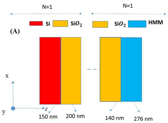
A schematic diagram of the PC1 and PC2. Each PC composed of one period. PC1 consists of Si and (,) with ,, and ( and HMM) with , for the second PC2.
Topological characteristics of the designed 1D PCs
Now, we have introduced the optical features of our designed based on the previous mathematical formulism. Meanwhile, the transmittance characteristics of the two 1D-PCs were calculated. Then, the topological features of our considered TPCs are demonstrated. Furthermore, we have illustrated how the transmittance characteristics of the TPC are affected by the thicknesses of the considered materials, the periodicity of the HMM and the filling ratio of Si through the HMM layer.
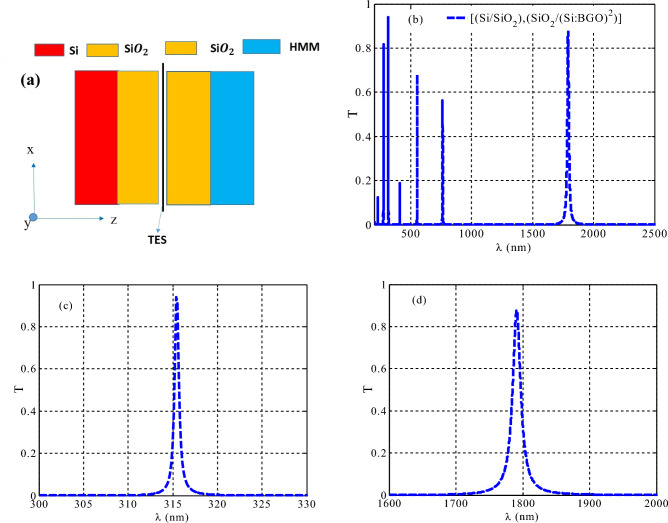
The block diagram of 1D TPCs, which is produced by arranging two PCs (PC1 and PC2), is shown in Fig. 2a. Here, we have considered only one unit cell in each PCs (PC1 and PC2) which make the suggested design novel and promising regarding the manufacturing procedure. Notably, most of the designed sensing tools based on photonic and phononic structures are essentially designed using a relatively large number of unit cells i.e., N = 4 or more. Here, the transmittance characteristics of the suggested structure show the emergence of many resonant modes with various transmittance values through the considered wavelengths, as shown in Fig. 2b. These modes are known as topological edge states (TESs). These modes can be considered for detection and sensing of some varying physical parameters such as temperature, electric field, magnetic field, and pressure as well. Next, as seen in Fig. 2c,d, the induced TES is visible throughout the whole near-infrared spectrum at specific wavelengths, such as λ = 315.4 nm and λ = 1791 nm. Figure 2c,d depict the zoomed-in form of the TES, of full width at half maximum values (FWHM = 0.7 nm and FWHM = 14 nm), and (93.9% and 87.6%) transmission values, respectively. This profound leads to resonant at heterostructure interfaces70,98. For the first time, the photonic TES in the 1D PCs heterostructure was predicted based on explanation of Zak phase99. They provide a workable technique for building a TES in various 1D PC heterostructure bandgaps100–102. It offers a new way to control photon transit because the local TES can induce photons that are carried by the PCs at bandgap frequencies. Nonetheless, the Zak phases, or the band topological phases, of the two PCs demonstrate that, in terms of topological symmetry, PC1's arrangement differs from PC2's arrangement. Meanwhile, TES are capable of inducing photons of a specified wavelength to be localized within the PBG99. Notably, Zak phase that also known as the TES needs for combining two PCs of different configurations in terms of the topological symmetry99–102. On other words, the construction of two PCs with overlapping PBGs of opposing topological phase bandgap leads to the appearance of this interface state100. The sum of the Zak phases of all the bands below the nth gap can be used to establish the topological symmetry sign of the nth gap99. Meanwhile, the TES appears inside a distinct frequency at nonzero value of the two gaps of PC1 and PC2, overlapping frequencies and the gap topological invariants of the two PCs have opposite signs99.
Figure 2.
(a) Diagrammatic representations of the 1D TPC structures, (b) the transmittance characteristics of a 1D TPCs and (c,d) the zoom-in of resonant sharp TES modes of 1D TPCs which consisted of one period for each PC.
Here, the heterostructure transmission characteristics are investigated in Fig. 2c,d. Transmission modes with opposing gap topological parameters of PC1 and PC2 are observed at = 315.4 nm and 1791 nm. The transmission mode indicates that the TES is located at the heterostructure related of the two PCs, even though it is in the bandgap overlap region; the TES guided the photons through. The resulting TES has an outstanding quality factor (Q), equal to , and an outstanding transmission value extend up to 93.9%. The proportion of the resonant wavelength to FWHM is defined as the quality factor (Q) of the considered mode. Right now, we have a wide range of resonant wavelengths with high quality factors (Q) and good transmission values. Although TES has a high Q value, some transmission value problems may prevent it from being used extensively in industrial processes. To improve this structure's performance in applications where it serves as a sensing tool, topological 1D PCs are advised.
The impact of changing the thickness of Si layer on the topological features of the designed structure
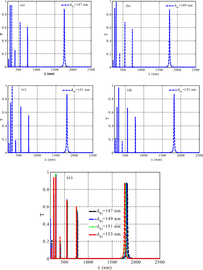
Figure 3 explains the transmittance properties of the proposed TPC design at different Si layer thicknesses of 147 nm, 149 nm, 151 nm, and 153 nm. Figure 3 shows the emergence of seven resonant modes, as shown in Fig. 3a. The number of resonant modes becomes constant as the thickness of Si increases to 149 nm, 151 nm, and 153 nm, but the intensity of transmission varies slightly, as seen in Fig. 3b–d, respectively. Moreover, there is a little shift in their spectral position with the increase in the thickness of Si layer as shown in Fig. 3e. However, this little shift does not effect on the topological features of the designed TPCs. For consideration, we have a localization for all the resonant modes. Conversely, as the thickness of the Si layer increases, each peak maintains its position. The position of the resonant modes is shown in Fig. 3e with a slight decrease in transmission intensity. Consequently, a good qualitative information about the stability and topological protection of the edge modes is obtained. In particular, the TESs may provide some little changes in their characteristics regarding the geometrical changes or construction flaws.
Figure 3.
The transmittance properties of a one-dimensional TPC design contains HMM at different thickness values of the Si layer.
The effect of varying SiO2 layer’s thickness on the topological characteristics
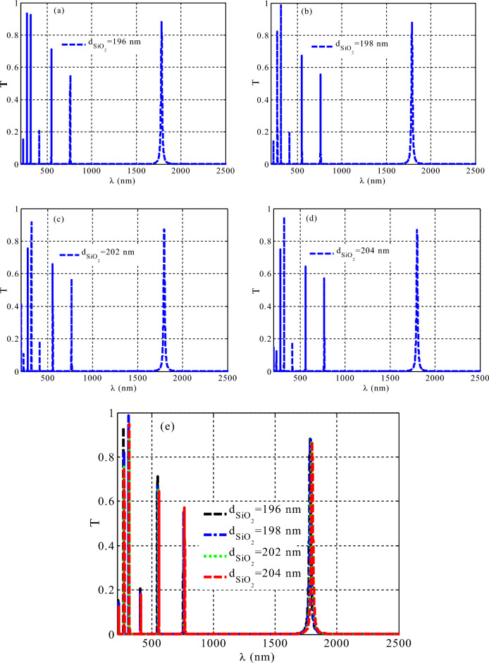
The estimated PC design transmittance properties at various layer thicknesses in PC1 are investigated in Fig. 4 as , with a fixed thicknesses of other layers in PC1 and PC2. An increase in results in no change in the number and position of resonant modes, as Fig. 4 illustrates. Figure 4a illustrates that there are seven resonant modes at . The number of resonant modes remains seven as the thickness of the layer increased to 198 nm, 202 nm, and 204 nm, but the intensity of transmittance changed slightly, as seen in Fig. 4b–d, respectively. To sum up, Fig. 4e displays the response of the resonant modes at different thickness of SiO2 layer. The figure shows a small reduction in their transmission intensity. However, this decrease in transmittance does not effect on the survival of the edge mode. In summary, our results guarantee the robustness of the interface mode towards increasing the thickness of in PC1. This implies that light moves along the interface with minimal energy losses, without reflection, and with small changes in its energy flux.
Figure 4.
The transmittance properties of a one-dimensional TPC design contains HMM at different thickness values of the layer in PC1.
The impact of Si filling ratio in the HMM layer on the topological features
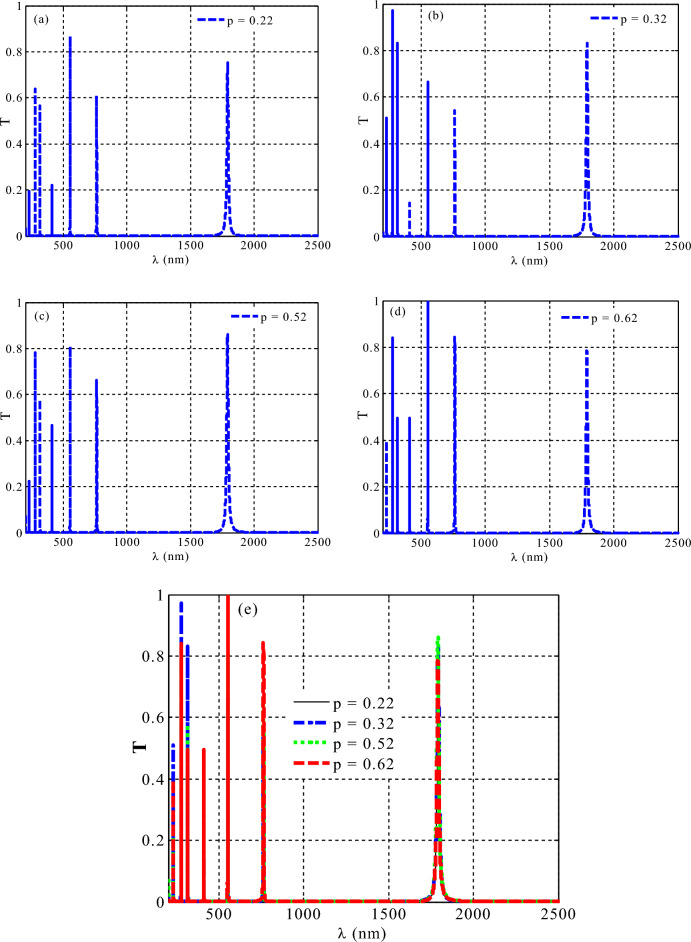
Here, we describe the properties of the obtained resonant modes and explain how our proposed structure's optical transmittance is affected by the Si filling ratio in the HMM layer. When the Si filling ratio is altered, Fig. 5 shows the response of the amount of resonant modes and their transmittance intensity regarding this change. In fact, the effective permittivity of the HMM layer is significantly affected by changes in the filling ratio as observed in Eqs. 2 and 3. However, Fig. 5 shows that, the increase in the filling ratio of the Si is not almost effective on the transmittance properties of the resonant mode despite its significant contribution on the permittivity components of the HMM. This response could be due to the topological feature of our 1D TPCs that is robust against the geometrical changes. In this regard, as shown in Fig. 5a–d, respectively, the number of the resonant peak stays constant at 7, but with slightly difference in their transmittance intensities. Also, Fig. 5e summarize this result. Consequently, remarkable qualitative information about the robustness and topological protection of the edge modes becomes available.
Figure 5.
The transmittance properties of a one-dimensional TPC design at various filling ratio of Si inside the HMM layer.
The effect of changing the periodicity of the HMM on the topological properties
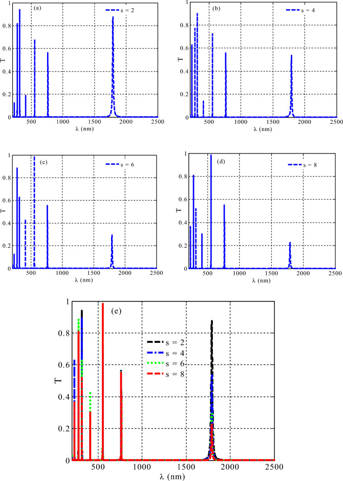
Figure 6 shows that, as the periodicity number of the HMM layer (S) increases, the number of resonant modes remains constant with a little changes in their transmittivity. As can be seen in Fig. 6a, the periodic number of HMM S = 2 produces 7 resonant modes. Following this, as investigated in Fig. 6b–d, the number of resonant modes stabilized at 7 with a smaller reduction in transmission intensity as S increases to 4, 6, and 10, respectively. The resonant modes were localized at the same spectral wavelength despite the increase in the HMM’s periodicity as depicted in the summarized Fig. 6e. The increasing periodicity of the HMM suggests that the thickness of this layer is increasing. Then, as reference95 illustrates, we can anticipate that the number of resonant modes will begin small and increase as the periodicity of the HMM increases. In our work, this transmittance decrease has no effect on the ability to survive of the edge mode as the thickness of the HMM layer increases. Overall, our results show that the robustness of the interface mode is shielded from adjustments that increase the HMM's periodicity, which may be helpful in certain applications like temperature sensor and optical filters as well.
Figure 6.
1D TPCs transmittance characteristic includes various periodicity of HMM.
The impact of varying the thickness of SiO2 layer in PC2 on the topological features of the designed structure
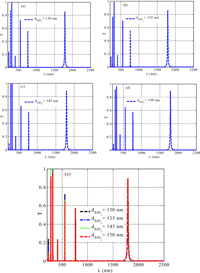
Next, Fig. 7 shows the predicted PC design transmittance properties at different layer thicknesses in PC2 as , while PC1 and the (HMM) layer thicknesses stay fixed at their initial values. Figure 7 shows that there is no variation in the number and position of resonant modes with an increase in . There are 7 resonant modes at , as shown in Fig. 7a. As the thickness of the layer raises more to 135 nm, 145 nm, and 150 nm, the number of resonant modes is still seven, as can be seen in Fig. 7b–d, respectively, however their intensities are slightly decreased. Then, Fig. 7e indicates the role of SiO2 thickness on the characteristics of these resonant modes. The survival of the edge mode peak is unaffected by this transmittance decrease. To sum up, our findings ensure that the interface mode remains stable as the thickness of in PC2 increases. This result investigates that light travels along the interface with negligible energy flux variations, no reflection, and minimal energy losses.
Figure 7.
The impact of layer’s thickness in PC2 on the topological features of the designed 1D TPCs.
The effect of changing the thickness of the HMM on the topological features
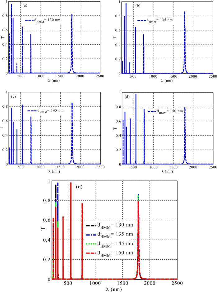
Finally, the transmittance characteristics of the suggested TPC design at various HMM layer thicknesses of 130, 135, 145, and 150 nm are described in Fig. 8. As seen in Fig. 8a, there are seven resonant modes. As the thickness of HMM layer increases to the number of resonant modes remains constant, as shown in Fig. 8b–d, respectively. On the other hand, each peak holds its position as the HMM layer increases. Figure 8e displays the position of all of the resonant modes along with a small transmission intensity decrease. This yields robust qualitative information about the topological stability and protection of the edge modes.
Figure 8.
The transmittance spectra of the proposed 1D TPCs at different thicknesses of the HMM’s layer.
The performance of the suggested 1D TPC temperature sensor
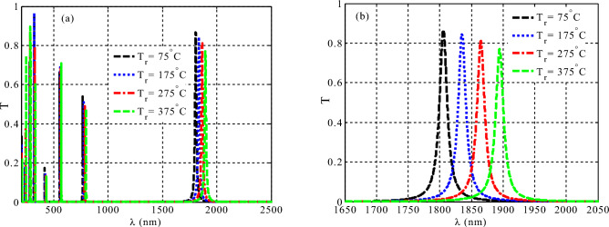
In this subsection, we have discussed the response of the resonant modes regarding the temperature variations as shown in Fig. 9. Here, the temperature change is classified as an external parameter rather than a geometrical change. This parameter can lead to a significant change on the optical properties of the considered materials specifically their indices of refraction due to the thermos-optic effect as indicated in Eq. (5). Therefore, the changes in the indices of refraction of the constituent materials could give rise to some changes in the transmittance values and the spectral positions as well of the resonant modes. This response could be promising towards considering this design as a promising temperature sensor with a topological feature of some robustness against the geometrical tolerance. The transmittance spectra of our designed 1D TPCs at different temperatures are displayed in Fig. 9. For PC1 thicknesses, the values are , and for PC2, the values are, , . Figure 9b displays an enlarged version of the gearbox modes from Fig. 9a. At Tr = 75 °C, a resonant transmission peak is present at wavelength 1805 nm. The resonant transmission mode's wavelength shifting as temperature rises (red shifting with temperature rise). A resonant transmission mode is obtained at 1835 nm at Tr = 175 °C, indicating a 30 nm wavelength shift in comparison to Tr = 75 °C. Consequently, a resonant transmission peak is obtained at 1865 nm and 1894 nm, respectively, at Tr = 275 °C and 375 °C. Table 1 shows the wavelength at which resonant transmission modes at various temperatures. Moreover, this table indicates the overall performance of the considered sensor in the vicinity of sensitivity, quality factor and figure of merit as well. In this regard, the investigated results show a relatively high sensitivity of 0.27 nm/°C besides a Q value of 133. Here, a small value of quality factor is obtained due to the increased value of FWHM because our design contains only 2-unit cells, one for PC1 and the other for PC2. In particular, small values of periodicity could give rise to large values of FWHM. Finally, Table 2 compares the main performance parameters of the suggested temperature sensor to those of previously published temperature sensors in order to evaluate the temperature-sensing capabilities of the proposed temperature sensor. Table 2 clearly shows that the designed structure performs better and more sensitive to temperature when it is topologically symmetric. In contrast to the earlier research mentioned in Table 2, the suggested design provides a little sensitivity compared with some of these published results. However, we believe that our suggested temperature sensor could be of a potential interest compared with tis counterparts. In particular, it possesses the robustness and stability against the geometrical tolerance unlike these designs. In addition, our designed temperature sensor contains a few number of layers. Therefore, our designed 1D TPC temperature sensor could provide some advantages through the manufacturing procedure.
Figure 9.
The transmittance characteristics of the designed 1D TPC temperature sensor at different values of temperature, (a) for a wide range of the incident electromagnetic waves, and (b) zoomed view of the resonant mode.
Table 1.
The values of resonant peak, sensitivity, Q-value, FOM and FWHM at various temperatures.
| Temperature (°C) | Resonant peak (nm) | Sensitivity (nm/°C) | Q-value | FOM | FWHM (nm) |
|---|---|---|---|---|---|
| 25 | 1790 | – | – | – | 14 |
| 75 | 1806 | 0.12 | 120.4 | 0.008 | 15 |
| 175 | 1835 | 0.19 | 122.33 | 0.0126 | 15 |
| 275 | 1865 | 0.26 | 133.21 | 0.018 | 14 |
| 375 | 1895 | 0.271 | 126.33 | 0.0181 | 15 |
Table 2.
Comparison of our result with some the previous published ones.
| Ref. no./year | Sensitivity (nm/°C) | Topological design | Temperature range (°C) |
|---|---|---|---|
| 103/2016 | -2.08 | Not achieved | 25–60 |
| 104/2018 | 1.5 | Not achieved | 35–100 |
| 105/2020 | 0.36 | Not achieved | 10–80 |
| 106/2021 | 3.2 | Not achieved | 20–50 |
| 107/2022 | 1.41 | Not achieved | 20–80 |
| 108/2022 | -0.306 | Not achieved | 40–50 |
| 109/2023 | 5.2 | Not achieved | 10–60 |
| 110/2023 | 7.13 | Not achieved | 0–70 |
| 111/2023 | 0.173 | Not achieved | 75–375 |
| 112/2023 | 0.085 | Not achieved | 25–900 |
| This work | 0.27 | Achieved | 75–375 |
Conclusion
Lastly, we theoretically analyzed the transmittance properties of a one-dimensional TPC at visible light and NIR. Our designed TPCs contains two different PCs. We compute the properties of resonant modes with stability in our design using the characteristic matrix model and the effective medium theory. Furthermore, we examine the effects of and Si layer thickness, HMM thickness, Si layer filling ratio, and HMM periodicity on the characteristics of the emerged resonant modes. Interestingly, our numerical findings demonstrate that our designed 1D TPCs provide profound stability and robustness as well against the geometrical changes. In comparison with the traditional uniform PC, the proposed topological PC exhibits a considerably lower threshold and higher manufacturing facilities tolerance. Thus, our structure can be promising as temperature sensor with a relatively high sensitivity of 0.27 nm/°C besides a Q value of 133.
Supplementary Information
Acknowledgements
The authors extend their appreciation to King Saud University for funding this work through Researchers Supporting Project number (RSP2024R133), King Saud University, Riyadh, Saudi Arabia.
Author contributions
Project administration, A. G. M., A. M. E., A. H. A., W. A. Z., M. R. A., A. M., and H. A. E.; supervision, A. M. E., A. H. A., W. A. Z., M. R. A., A. M., and H. A. E.; software, A. G. M., A. M., and H. A. E.; visualization, A. G. M., A. M., and H. A. E.; writing—review and editing; A. G. M., A. M. E., A. H. A., W. A. Z., M. R. A., A. M., and H. A. E.; writing—original draft, A. G. M.; methodology, A. G. M., A. M., and H. A. E.; All authors have read and agreed to the published version of the manuscript.
Data availability
The datasets used and/or analyzed during the current study available from the corresponding author on reasonable request.
Competing interests
The authors declare no competing interests.
Footnotes
Publisher's note
Springer Nature remains neutral with regard to jurisdictional claims in published maps and institutional affiliations.
Contributor Information
Wail Al Zoubi, Email: wailalzoubi@ynu.ac.kr.
Ahmed Mehaney, Email: Ahmed011236@science.bsu.edu.eg.
Supplementary Information
The online version contains supplementary material available at 10.1038/s41598-024-69751-3.
References
- 1.Tang, G. J. et al. Topological photonic crystals: Physics, designs, and applications. Laser Photon. Rev.16, 2100300 (2022). [Google Scholar]
- 2.Klitzing, K. V., Dorda, G. & Pepper, M. New method for high-accuracy determination of the fine-structure constant based on quantized Hall resistance. Phys. Rev. Lett.45, 494 (1980). [Google Scholar]
- 3.Laughlin, R. B. Quantized Hall conductivity in two dimensions. Phys. Rev. B23, 5632 (1981). [Google Scholar]
- 4.Thouless, D. J., Kohmoto, M., Nightingale, M. P. & den Nijs, M. Quantized Hall conductance in a two-dimensional periodic potential. Phys. Rev. Lett.49, 405 (1982). [Google Scholar]
- 5.Tsui, D. C., Stormer, H. L. & Gossard, A. C. Two-dimensional magnetotransport in the extreme quantum limit. Phys. Rev. Lett.48, 1559 (1982). [Google Scholar]
- 6.Laughlin, R. B. Anomalous quantum Hall effect: An incompressible quantum fluid with fractionally charged excitations. Phys. Rev. Lett.50, 1395 (1983). [Google Scholar]
- 7.Haldane, F. D. M. Model for a quantum Hall effect without Landau levels: Condensed-matter realization of the" parity anomaly". Phys. Rev. Lett.61, 2015 (1988). [DOI] [PubMed] [Google Scholar]
- 8.Jiang, L. et al. Majorana fermions in equilibrium and in driven cold-atom quantum wires. Phys. Rev. Lett.106, 220402 (2011). [DOI] [PubMed] [Google Scholar]
- 9.Goldman, N., Budich, J. C. & Zoller, P. Topological quantum matter with ultracold gases in optical lattices. Nat. Phys.12, 639–645 (2016). [Google Scholar]
- 10.Fleury, R., Sounas, D. L., Sieck, C. F., Haberman, M. R. & Alù, A. Sound isolation and giant linear nonreciprocity in a compact acoustic circulator. Science343, 516–519 (2014). [DOI] [PubMed] [Google Scholar]
- 11.Ni, X. et al. Topologically protected one-way edge mode in networks of acoustic resonators with circulating air flow. N. J. Phys.17, 053016 (2015). [Google Scholar]
- 12.Wang, P., Lu, L. & Bertoldi, K. Topological phononic crystals with one-way elastic edge waves. Phys. Rev. Lett.115, 104302 (2015). [DOI] [PubMed] [Google Scholar]
- 13.Yang, Z. et al. Topological acoustics. Phys. Rev. Lett.114, 114301 (2015). [DOI] [PubMed] [Google Scholar]
- 14.Khanikaev, A. B., Fleury, R., Mousavi, S. H. & Alu, A. Topologically robust sound propagation in an angular-momentum-biased graphene-like resonator lattice. Nat. Commun.6, 8260 (2015). [DOI] [PMC free article] [PubMed] [Google Scholar]
- 15.Pal, R. K. & Ruzzene, M. Edge waves in plates with resonators: An elastic analogue of the quantum valley Hall effect. N. J. Phys.19, 025001 (2017). [Google Scholar]
- 16.Qian, K., Apigo, D. J., Prodan, C., Barlas, Y. & Prodan, E. Topology of the valley-Chern effect. Phys. Rev. B98, 155138 (2018). [Google Scholar]
- 17.Mousavi, S. H., Khanikaev, A. B. & Wang, Z. Topologically protected elastic waves in phononic metamaterials. Nat. Commun.6, 8682 (2015). [DOI] [PMC free article] [PubMed] [Google Scholar]
- 18.Haldane, F. D. M. & Raghu, S. Possible realization of directional optical waveguides in photonic crystals with broken time-reversal symmetry. Phys. Rev. Lett.100, 013904 (2008). [DOI] [PubMed] [Google Scholar]
- 19.Di Pietro, P. et al. Observation of Dirac plasmons in a topological insulator. Nat. Nanotechnol.8, 556–560 (2013). [DOI] [PubMed] [Google Scholar]
- 20.Poddubny, A., Miroshnichenko, A., Slobozhanyuk, A. & Kivshar, Y. Topological Majorana states in zigzag chains of plasmonic nanoparticles. ACS Photonics1, 101–105 (2014). [Google Scholar]
- 21.Stauber, T. Plasmonics in Dirac systems: From graphene to topological insulators. J. Phys. Condensed Matter26, 123201 (2014). [DOI] [PubMed] [Google Scholar]
- 22.Ling, C., Xiao, M., Chan, C. T., Yu, S. F. & Fung, K. H. Topological edge plasmon modes between diatomic chains of plasmonic nanoparticles. Opt. Express23, 2021–2031 (2015). [DOI] [PubMed] [Google Scholar]
- 23.Sinev, I. S. et al. Mapping plasmonic topological states at the nanoscale. Nanoscale7, 11904–11908 (2015). [DOI] [PubMed] [Google Scholar]
- 24.Gao, W. et al. Photonic Weyl degeneracies in magnetized plasma. Nat. Commun.7, 12435 (2016). [DOI] [PMC free article] [PubMed] [Google Scholar]
- 25.Siroki, G., Lee, D., Haynes, P. & Giannini, V. Single-electron induced surface plasmons on a topological nanoparticle. Nat. Commun.7, 12375 (2016). [DOI] [PMC free article] [PubMed] [Google Scholar]
- 26.Jin, D. et al. Infrared topological plasmons in graphene. Phys. Rev. Lett.118, 245301 (2017). [DOI] [PubMed] [Google Scholar]
- 27.Pan, D., Yu, R., Xu, H. & García de Abajo, F. J. Topologically protected Dirac plasmons in a graphene superlattice. Nat. Commun.8, 1243 (2017). [DOI] [PMC free article] [PubMed] [Google Scholar]
- 28.Wu, X. et al. Direct observation of valley-polarized topological edge states in designer surface plasmon crystals. Nat. Commun.8, 1304 (2017). [DOI] [PMC free article] [PubMed] [Google Scholar]
- 29.Jung, M., Fan, Z. & Shvets, G. Midinfrared plasmonic valleytronics in metagate-tuned graphene. Phys. Rev. Lett.121, 086807 (2018). [DOI] [PubMed] [Google Scholar]
- 30.Jung, M., Gladstone, R. G. & Shvets, G. Nanopolaritonic second-order topological insulator based on graphene plasmons. Adv. Photon.2, 046003–046003 (2020). [Google Scholar]
- 31.Fang, K., Yu, Z. & Fan, S. Realizing effective magnetic field for photons by controlling the phase of dynamic modulation. Nat. Photon.6, 782–787 (2012). [Google Scholar]
- 32.Ozawa, T., Price, H. M., Goldman, N., Zilberberg, O. & Carusotto, I. Synthetic dimensions in integrated photonics: From optical isolation to four-dimensional quantum Hall physics. Phys. Rev. A93, 043827 (2016). [Google Scholar]
- 33.Wang, Q., Xiao, M., Liu, H., Zhu, S. & Chan, C. T. Optical interface states protected by synthetic Weyl points. Phys. Rev. X7, 031032 (2017). [Google Scholar]
- 34.Lin, Q., Sun, X.-Q., Xiao, M., Zhang, S.-C. & Fan, S. A three-dimensional photonic topological insulator using a two-dimensional ring resonator lattice with a synthetic frequency dimension. Sci. Adv.4, 2774 (2018). [DOI] [PMC free article] [PubMed] [Google Scholar]
- 35.Ozawa, T. & Price, H. M. Topological quantum matter in synthetic dimensions. Nat. Rev. Phys.1, 349–357 (2019). [Google Scholar]
- 36.Lustig, E. & Segev, M. Topological photonics in synthetic dimensions. Adv. Opt. Photon.13, 426–461 (2021). [Google Scholar]
- 37.Hafezi, M., Demler, E. A., Lukin, M. D. & Taylor, J. M. Robust optical delay lines with topological protection. Nat. Phys.7, 907–912 (2011). [Google Scholar]
- 38.Liang, G. & Chong, Y. Optical resonator analog of a two-dimensional topological insulator. Phys. Rev. Lett.110, 203904 (2013). [DOI] [PubMed] [Google Scholar]
- 39.Gao, F. et al. Probing topological protection using a designer surface plasmon structure. Nat. Commun.7, 11619 (2016). [DOI] [PMC free article] [PubMed] [Google Scholar]
- 40.Mittal, S., Goldschmidt, E. A. & Hafezi, M. A topological source of quantum light. Nature561, 502–506 (2018). [DOI] [PubMed] [Google Scholar]
- 41.Yang, H. et al. Optically reconfigurable spin-valley Hall effect of light in coupled nonlinear ring resonator lattice. Phys. Rev. Lett.127, 043904 (2021). [DOI] [PubMed] [Google Scholar]
- 42.Nalitov, A., Malpuech, G., Terças, H. & Solnyshkov, D. Spin-orbit coupling and the optical spin hall effect in photonic graphene. Phys. Rev. Lett.114, 026803 (2015). [DOI] [PubMed] [Google Scholar]
- 43.Sanvitto, D. & Kéna-Cohen, S. The road towards polaritonic devices. Nat. Mater.15, 1061–1073 (2016). [DOI] [PubMed] [Google Scholar]
- 44.Milićević, M. et al. Orbital edge states in a photonic honeycomb lattice. Phys. Rev. Lett.118, 107403 (2017). [DOI] [PubMed] [Google Scholar]
- 45.Solnyshkov, D. D., Nalitov, A. V. & Malpuech, G. Kibble-Zurek mechanism in topologically nontrivial zigzag chains of polariton micropillars. Phys. Rev. Lett.116, 046402 (2016). [DOI] [PubMed] [Google Scholar]
- 46.Rechtsman, M. C. et al. Photonic Floquet topological insulators. Nature496, 196–200 (2013). [DOI] [PubMed] [Google Scholar]
- 47.Zhong, H. et al. Rabi-like oscillation of photonic topological valley Hall edge states. Opt. Lett.44, 3342–3345 (2019). [DOI] [PubMed] [Google Scholar]
- 48.Gao, W. et al. Topological photonic phase in chiral hyperbolic metamaterials. Phys. Rev. Lett.114, 037402 (2015). [DOI] [PubMed] [Google Scholar]
- 49.Poshakinskiy, A., Poddubny, A., Pilozzi, L. & Ivchenko, E. Radiative topological states in resonant photonic crystals. Phys. Rev. Lett.112, 107403 (2014). [DOI] [PubMed] [Google Scholar]
- 50.Borges-Silva, D., Costa, C. H. O. & Bezerra, C. G. Robust topological edge states in C 6 photonic crystals. Photonics1, 961 (2023). [DOI] [PMC free article] [PubMed] [Google Scholar]
- 51.Dong, J.-W. et al. Conical dispersion and effective zero refractive index in photonic quasicrystals. Phys. Rev. Lett.114, 163901 (2015). [DOI] [PubMed] [Google Scholar]
- 52.Lu, L. et al. Symmetry-protected topological photonic crystal in three dimensions. Nat. Phys.12, 337–340 (2016). [Google Scholar]
- 53.Chiasera, A. et al. Coherent emission from fully Er3+ doped monolithic 1-D dielectric microcavity fabricated by rf-sputtering. Opt. Mater.87, 107–111 (2019). [Google Scholar]
- 54.Davoyan, A. R. & Engheta, N. Theory of wave propagation in magnetized near-zero-epsilon metamaterials: Evidence for one-way photonic states and magnetically switched transparency and opacity. Phys. Rev. Lett.111, 257401 (2013). [DOI] [PubMed] [Google Scholar]
- 55.Guo, Q., Gao, W., Chen, J., Liu, Y. & Zhang, S. Line degeneracy and strong spin-orbit coupling of light with bulk bianisotropic metamaterials. Phys. Rev. Lett.115, 067402 (2015). [DOI] [PubMed] [Google Scholar]
- 56.Liu, C., Gao, W., Yang, B. & Zhang, S. Disorder-induced topological state transition in photonic metamaterials. Phys. Rev. Lett.119, 183901 (2017). [DOI] [PubMed] [Google Scholar]
- 57.Yang, B. et al. Ideal Weyl points and helicoid surface states in artificial photonic crystal structures. Science359, 1013–1016 (2018). [DOI] [PubMed] [Google Scholar]
- 58.Li, C. et al. Subwavelength silicon photonics for on-chip mode-manipulation. PhotoniX2, 1–35 (2021). [Google Scholar]
- 59.Yang, B. et al. Direct observation of topological surface-state arcs in photonic metamaterials. Nat. Commun.8, 97 (2017). [DOI] [PMC free article] [PubMed] [Google Scholar]
- 60.Polini, M., Guinea, F., Lewenstein, M., Manoharan, H. C. & Pellegrini, V. Artificial honeycomb lattices for electrons, atoms and photons. Nat. Nanotechnol.8, 625–633 (2013). [DOI] [PubMed] [Google Scholar]
- 61.Lu, L., Joannopoulos, J. D. & Soljačić, M. Topological photonics. Nat. Photon.8, 821–829 (2014). [Google Scholar]
- 62.Longhi, S. Zak phase of photons in optical waveguide lattices. Opt. Lett.38, 3716–3719 (2013). [DOI] [PubMed] [Google Scholar]
- 63.Verbin, M., Zilberberg, O., Kraus, Y. E., Lahini, Y. & Silberberg, Y. Observation of topological phase transitions in photonic quasicrystals. Phys. Rev. Lett.110, 076403 (2013). [DOI] [PubMed] [Google Scholar]
- 64.Ochiai, T. Broken symmetry and topology in photonic analog of graphene. Int. J. Mod. Phys. B28, 1441004 (2014). [Google Scholar]
- 65.Sohrabi, F., Hamidi, S. M., Asgari, N., Ansari, M. A. & Gachiloo, R. One dimensional photonic crystal as an efficient tool for in-vivo optical sensing of neural activity. Opt. Mater.96, 109275 (2019). [Google Scholar]
- 66.Shen, H., Wang, Z., Wu, Y. & Yang, B. One-dimensional photonic crystals: fabrication, responsiveness and emerging applications in 3D construction. RSC Adv.6, 4505–4520 (2016). [Google Scholar]
- 67.Tabassum, S., Nayemuzzaman, S., Kala, M., Kumar Mishra, A. & Mishra, S. K. Metasurfaces for sensing applications: Gas, bio and chemical. Sensors22, 6896 (2022). [DOI] [PMC free article] [PubMed] [Google Scholar]
- 68.Harris, J. M., Lopez, G. P. & Reichert, W. M. Silica-dispersed glucose oxidase for glucose sensing: In vitro testing in serum and blood and the effect of condensation pH. Sens. Actuators B Chem.174, 373–379 (2012). [DOI] [PMC free article] [PubMed] [Google Scholar]
- 69.Jia, W.-Z., Wang, K., Zhu, Z.-J., Song, H.-T. & Xia, X.-H. One-step immobilization of glucose oxidase in a silica matrix on a Pt electrode by an electrochemically induced sol−gel process. Langmuir23, 11896–11900 (2007). [DOI] [PubMed] [Google Scholar]
- 70.Elshahat, S., Mohamed, Z. E. A., Abd-Elnaiem, A. M., Ouyang, Z. & Almokhtar, M. One-dimensional topological photonic crystal for high-performance gas sensor. Micro Nanostruct.172, 207447 (2022). [Google Scholar]
- 71.Wang, X. et al. Enlargement of omnidirectional total reflection frequency range in one-dimensional photonic crystals by using photonic heterostructures. Appl. Phys. Lett.80, 4291–4293 (2002). [Google Scholar]
- 72.Zhang, J.-L. et al. Two-dimensional complete band gaps in one-dimensional metal-dielectric periodic structures. Appl. Phys. Lett.92, 1 (2008). [Google Scholar]
- 73.Jiang, H., Chen, H., Li, H., Zhang, Y. & Zhu, S. Omnidirectional gap and defect mode of one-dimensional photonic crystals containing negative-index materials. Appl. Phys. Lett.83, 5386–5388 (2003). [Google Scholar]
- 74.Lopez, C. Materials aspects of photonic crystals. Adv. Mater.15, 1679–1704 (2003). [Google Scholar]
- 75.Shelby, R. A., Smith, D. R. & Schultz, S. Experimental verification of a negative index of refraction. Science292, 77–79 (2001). [DOI] [PubMed] [Google Scholar]
- 76.Povinelli, M. L., Johnson, S. G., Joannopoulos, J. & Pendry, J. Toward photonic-crystal metamaterials: Creating magnetic emitters in photonic crystals. Appl. Phys. Lett.82, 1069–1071 (2003). [Google Scholar]
- 77.Madani, A. & Entezar, S. R. Optical properties of one-dimensional photonic crystals containing graphene-based hyperbolic metamaterials. Photon. Nanostruct. Fund. Appl.25, 58–64 (2017). [DOI] [PubMed] [Google Scholar]
- 78.Wu, F. et al. Effective optical nihility media realized by one-dimensional photonic crystals containing hyperbolic metamaterials. Opt. Express28, 33198–33207 (2020). [DOI] [PubMed] [Google Scholar]
- 79.Li, J., Zhou, L., Chan, C. T. & Sheng, P. Photonic band gap from a stack of positive and negative index materials. Phys. Rev. Lett.90, 083901 (2003). [DOI] [PubMed] [Google Scholar]
- 80.Jiang, H. et al. Properties of one-dimensional photonic crystals containing single-negative materials. Phys. Rev. E69, 066607 (2004). [DOI] [PubMed] [Google Scholar]
- 81.Ferrari, L., Wu, C., Lepage, D., Zhang, X. & Liu, Z. Hyperbolic metamaterials and their applications. Prog. Quant. Electron.40, 1–40 (2015). [Google Scholar]
- 82.Poddubny, A., Iorsh, I., Belov, P. & Kivshar, Y. Hyperbolic metamaterials. Nat. Photon.7, 948–957 (2013). [Google Scholar]
- 83.Hu, S., Du, S., Li, J. & Gu, C. Multidimensional image and beam splitter based on hyperbolic metamaterials. Nano Lett.21, 1792–1799 (2021). [DOI] [PubMed] [Google Scholar]
- 84.Shao, Z.-K. et al. A high-performance topological bulk laser based on band-inversion-induced reflection. Nat. Nanotechnol.15, 67–72 (2020). [DOI] [PubMed] [Google Scholar]
- 85.Xue, C.-H. et al. Dispersionless gaps and cavity modes in photonic crystals containing hyperbolic metamaterials. Phys. Rev. B93, 125310 (2016). [Google Scholar]
- 86.Wu, F. et al. Experimental demonstration of angle-independent gaps in one-dimensional photonic crystals containing layered hyperbolic metamaterials and dielectrics at visible wavelengths. Appl. Phys. Lett.112, 041902 (2018). [Google Scholar]
- 87.Wu, F. et al. Redshift gaps in one-dimensional photonic crystals containing hyperbolic metamaterials. Phys. Rev. Appl.10, 064022 (2018). [Google Scholar]
- 88.Lu, G. et al. Omnidirectional photonic bandgap in one-dimensional photonic crystals containing hyperbolic metamaterials. Opt. Express29, 31915–31923 (2021). [DOI] [PubMed] [Google Scholar]
- 89.Kumar, A. et al. Wide range temperature sensors based on one-dimensional photonic crystal with a single defect. Int. J. Microwave Sci. Technol.2012, 1–5 (2012). [Google Scholar]
- 90.Almawgani, A. H. et al. Sucrose concentration detector based on a binary photonic crystal with a defect layer and two nanocomposite layers. Zeitschrift für Naturforschung A77, 909–919 (2022). [Google Scholar]
- 91.Wu, J.-J. & Gao, J.-X. Low temperature sensor based on one-dimensional photonic crystals with a dielectric-superconducting pair defect. Optik126, 5368–5371 (2015). [Google Scholar]
- 92.El-Ghany, S.-S.A. Temperature sensors based on one dimensional photonic crystals with different double defects. J. Nanoelectron. Optoelectron.13, 221–228 (2018). [Google Scholar]
- 93.Charik, H., Bouras, M. & Bennacer, H. High-sensitive thermal sensor based on a 1D photonic crystal microcavity with nematic liquid crystal. Prog. Electromagn. Res. M100, 187–195 (2021). [Google Scholar]
- 94.Ahmed, A. M., Elsayed, H. A. & Mehaney, A. High-performance temperature sensor based on one-dimensional pyroelectric photonic crystals comprising Tamm/Fano resonances. Plasmonics16, 547–557 (2021). [Google Scholar]
- 95.Mohamed, A. G., Sabra, W., Mehaney, A., Aly, A. H. & Elsayed, H. A. Multiplication of photonic band gaps in one-dimensional photonic crystals by using hyperbolic metamaterial in IR range. Sci. Rep.13, 324 (2023). [DOI] [PMC free article] [PubMed] [Google Scholar]
- 96.Orfanidis, S. J. Electromagnetic waves and antennas (2002).
- 97.Babicheva, V. E., Shalaginov, M. Y., Ishii, S., Boltasseva, A. & Kildishev, A. V. Finite-width plasmonic waveguides with hyperbolic multilayer cladding. Opt. Express23, 9681–9689 (2015). [DOI] [PubMed] [Google Scholar]
- 98.Meade, R. D. V., Johnson, S. G., & Winn, J. N. Photonic crystals: Molding the flow of light (Princeton University Press, 2008).
- 99.Xiao, M., Zhang, Z. & Chan, C. T. Surface impedance and bulk band geometric phases in one-dimensional systems. Phys. Rev. X4, 021017 (2014). [Google Scholar]
- 100.Gao, W. S., Xiao, M., Chan, C. T. & Tam, W. Y. Determination of Zak phase by reflection phase in 1D photonic crystals. Opt. Lett.40, 5259–5262 (2015). [DOI] [PubMed] [Google Scholar]
- 101.Choi, K. H., Ling, C., Lee, K., Tsang, Y. H. & Fung, K. H. Simultaneous multi-frequency topological edge modes between one-dimensional photonic crystals. Opt. Lett.41, 1644–1647 (2016). [DOI] [PubMed] [Google Scholar]
- 102.Li, C., Hu, X., Yang, H. & Gong, Q. Unidirectional transmission in 1D nonlinear photonic crystal based on topological phase reversal by optical nonlinearity. AIP Adv.7, 1 (2017). [Google Scholar]
- 103.Yang, X., Lu, Y., Liu, B. & Yao, J. Temperature sensor based on photonic crystal fiber filled with liquid and silver nanowires. IEEE Photon. J.8, 1–9 (2016). [Google Scholar]
- 104.Wang, Y., Huang, Q., Zhu, W., Yang, M. & Lewis, E. Novel optical fiber SPR temperature sensor based on MMF-PCF-MMF structure and gold-PDMS film. Opt. Express26, 1910–1917 (2018). [DOI] [PubMed] [Google Scholar]
- 105.Osifeso, S., Chu, S., Prasad, A. & Nakkeeran, K. Surface Plasmon resonance-based temperature sensor with outer surface metal coating on multi-core photonic crystal fibre. Surfaces3, 337–351 (2020). [Google Scholar]
- 106.Wang, Q., Zhang, X., Yan, X., Wang, F. & Cheng, T. "Design of a surface plasmon resonance temperature sensor with multi-wavebands based on conjoined-tubular anti-resonance fiber. Photonics1, 231 (2021). [Google Scholar]
- 107.Gu, S. et al. Simultaneous measurement of magnetic field and temperature based on photonic crystal fiber plasmonic sensor with dual-polarized modes. Optik259, 169030 (2022). [Google Scholar]
- 108.Gao, P., Zheng, X., Liu, Y. & Wang, Z. Photonic crystal fiber refractive index temperature sensor based on double spherical cascade. Optik267, 169682 (2022). [Google Scholar]
- 109.Chao, C.-T.C. et al. Improving temperature-sensing performance of photonic crystal fiber via external metal-coated trapezoidal-shaped surface. Crystals13, 813 (2023). [Google Scholar]
- 110.Li, H. et al. High-sensitivity temperature sensor based on photonic crystal fiber filled with ethanol and toluene. ECS J. Solid State Sci. Technol.12, 127007 (2023). [Google Scholar]
- 111.Srivastava, S. K. design of temperature sensor based on one-dimensional photonic crystal containing Si–BGO layer. Mater. Open1, 2350003 (2023). [Google Scholar]
- 112.Aly, A. H., Mohamed, B., Al-Dossari, M. & Mohamed, D. A temperature sensor based on Si/PS/SiO2 photonic crystals. Sci. Rep.13, 21560 (2023). [DOI] [PMC free article] [PubMed] [Google Scholar]
Associated Data
This section collects any data citations, data availability statements, or supplementary materials included in this article.
Supplementary Materials
Data Availability Statement
The datasets used and/or analyzed during the current study available from the corresponding author on reasonable request.


